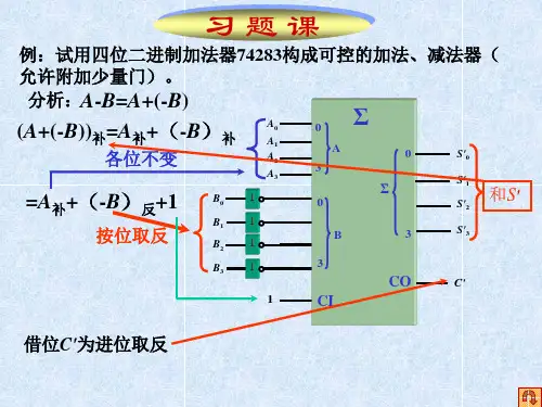
例:试用四位二进制加法器74283构成可控的加法、减法器(允许附加
- 格式:ppt
- 大小:203.00 KB
- 文档页数:4

可控加减法电路设计实验报告一、实验目的。
1.了解四位二进制数运算的基本原理,制定设计方案。
2.利用ISE软件进行可编程逻辑器件设计,完成逻辑仿真功能。
3.使用编译器将设计实现,下载到BASYS2实验板上进行调试和验证所设计的四位二进制数的运算。
二、实验器材。
1.Pentium—Ⅲ计算机一台;2.BASYS2 实验板一只;三、实验方案。
1.基本功能。
实现了两个四位二进制数的加减法运算,能够在输出端得出结果.2.清零功能。
利用一个微动开关,在逻辑程序中表示出当按下微动开关后两个操作数都变为零。
再调用以前的加法程序,即可实现输出结果清零。
3.用数码管显示。
编写程序,将数值转换为七段显示器显示。
将运算结果输送到数码管中。
值得注意的是四个数码管要显示不同的数字,就需要利用到人的视觉误差,做一些短暂的延时。
4.溢出显示。
本实验中,设计的是一个无符号数加减法器,因而其共有两种溢出情况一,减法时,减数大于被减数,针对这种情况可以利用比较大小进行溢出判断;二,加法时,被操作数之和大于15。
判断进位,如果进位为1则显示溢出,若反之,则不显示。
四、实验原理图。
五、实验模块说明及部分代码。
1.add1部分。
将输入的两个操作数相加并判断大小。
相加结果放在led中,进位放在carry中。
led[0]=num1[0]^num2[0];carry[0]=num1[0]&num2[0];led[1]=num1[1]^num2[1]^carry[0];carry[1]=(num1[1]&num2[1])|(carry[0]&(num1[1]^num2[1]));led[2]=num1[2]^num2[2]^carry[1];carry[2]=(num1[2]&num2[2])|(carry[1]&(num1[2]^num2[2]));led[3]=num1[3]^num2[3]^carry[2];if(add)begincarry[3]=(num1[3]&num2[3])|(carry[2]&(num1[3]^num2[3]));endif(sub)beginif(compare)carry[3]=1;elsecarry[3]=(num1[3]&num2[3])|(carry[2]&(num1[3]^num2[3]))&(~sub); 2.seg7ment。
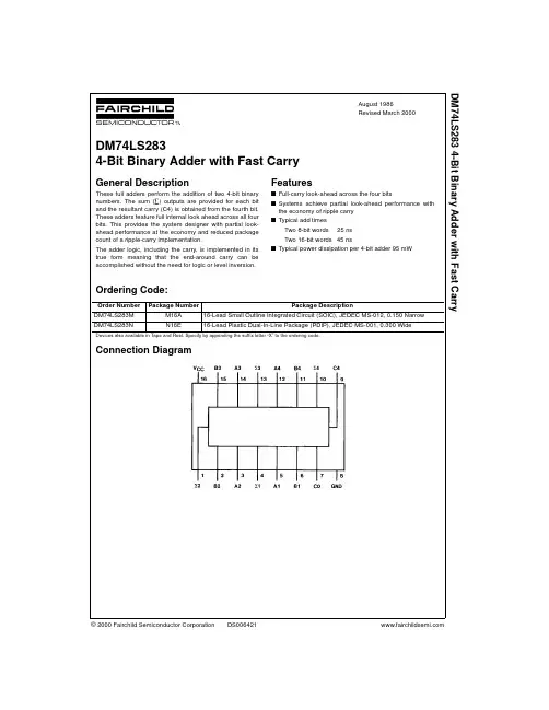
© 2000 Fairchild Semiconductor Corporation DS006421August 1986Revised March 2000DM74LS283 4-Bit Binary Adder with Fast CarryDM74LS2834-Bit Binary Adder with Fast CarryGeneral DescriptionThese full adders perform the addition of two 4-bit binary numbers. The sum (∑) outputs are provided for each bit and the resultant carry (C4) is obtained from the fourth bit.These adders feature full internal look ahead across all four bits. This provides the system designer with partial look-ahead performance at the economy and reduced package count of a ripple-carry implementation.The adder logic, including the carry, is implemented in its true form meaning that the end-around carry can be accomplished without the need for logic or level inversion.Featuress Full-carry look-ahead across the four bitss Systems achieve partial look-ahead performance with the economy of ripple carry s Typical add timesTwo 8-bit words25 nsTwo 16-bit words 45 nss Typical power dissipation per 4-bit adder 95 mWOrdering Code:Devices also available in T ape and Reel. Specify by appending the suffix letter “X” to the ordering code.Connection DiagramOrder Number Package NumberPackage DescriptionDM74LS283M M16A 16-Lead Small Outline Integrated Circuit (SOIC), JEDEC MS-012, 0.150 Narrow DM74LS283NN16E16-Lead Plastic Dual-In-Line Package (PDIP), JEDEC MS-001, 0.300 Wide 2D M 74L S 283Function TableH= HIGH Level, L = LOW LevelInput conditions at A1, B1, A2, B2, and C0 are used to determine outputs ∑1 and ∑2 and the value of the internal carry C2. The values at C2, A3, B3, A4, and B4 are then used to determine outputs ∑3, ∑4, and C4.Logic DiagramDM74LS283Absolute Maximum Ratings (Note 1)Note 1: The “Absolute Maximum Ratings” are those values beyond which the safety of the device cannot be guaranteed. The device should not be operated at these limits. The parametric values defined in the Electrical Characteristics tables are not guaranteed at the absolute maximum ratings.The “Recommended Operating Conditions” table will define the conditions for actual device operation.Recommended Operating ConditionsElectrical Characteristicsover recommended operating free air temperature range (unless otherwise noted)Note 2: All typicals are at V CC = 5V, T A = 25°C.Note 3: Not more than one output should be shorted at a time, and the duration should not exceed one second.Note 4: I CC1 is measured with all outputs OPEN, all B inputs LOW and all other inputs at 4.5V, or all inputs at 4.5V.Note 5: I CC2 is measured with all outputs OPEN and all inputs GROUNDED.Supply Voltage 7V Input Voltage7VOperating Free Air Temperature Range 0°C to +70°C Storage Temperature Range−65°C to +150°CSymbol ParameterMin Nom Max Units V CC Supply Voltage4.7555.25V V IH HIGH Level Input Voltage 2V V IL LOW Level Input Voltage 0.8V I OH HIGH Level Output Current −0.4mA I OL LOW Level Output Current 8mA T AFree Air Operating Temperature70°CSymbol ParameterConditionsMinTyp Max Units (Note 2)V I Input Clamp Voltage V CC = Min, I I = −18 mA −1.5V V OH HIGH Level V CC = Min, I OH = Max 2.73.4VOutput Voltage V IL = Max, V IH = Min V OLLOW Level V CC = Min, I OL = Max0.350.5Output VoltageV IL = Max, V IH = Min VI OL = 4 mA, V CC = Min 0.250.4I I Input Current @ Max V CC = Max A, B 0.2mA Input Voltage V I = 7V C00.1I IH HIGH Level V CC = Max A, B 40µA Input Current V I = 2.7V C020I IL LOW Level V CC = MaxA, B −0.8mA Input CurrentV I = 0.4V C0−0.4I OS Short Circuit Output Current V CC = Max −20−100mA I CC1Supply Current V CC = Max (Note 4)1934mA I CC2Supply CurrentV CC = Max (Note 5)2239mA 4D M 74L S 283Switching Characteristicsat V CC = 5V and T A = 25°CFrom (Input)R L = 2 k ΩSymbol ParameterTo (Output)C L = 15 pF C L = 50 pF UnitsMinMax MinMax t PLH Propagation Delay Time C0 to ∑1, ∑22428ns LOW-to-HIGH Level Output t PHL Propagation Delay Time C0 to ∑1, ∑22430ns HIGH-to-LOW Level Output t PLH Propagation Delay Time C0 to ∑32428ns LOW-to-HIGH Level Output t PHL Propagation Delay Time C0 to ∑32430ns HIGH-to-LOW Level Output t PLH Propagation Delay Time C0 to ∑42428ns LOW-to-HIGH Level Output t PHL Propagation Delay Time C0 to ∑42430ns HIGH-to-LOW Level Output t PLH Propagation Delay Time A i or B i to ∑i 2428ns LOW-to-HIGH Level Output t PHL Propagation Delay Time A i or B i to ∑i 2430ns HIGH-to-LOW Level Output t PLH Propagation Delay Time C0 to C41724ns LOW-to-HIGH Level Output t PHL Propagation Delay Time C0 to C41725ns HIGH-to-LOW Level Output t PLH Propagation Delay Time A i or B i to C41724ns LOW-to-HIGH Level Output t PHLPropagation Delay Time A i or B i to C41726ns HIGH-to-LOW Level OutputDM74LS283Physical Dimensions inches (millimeters) unless otherwise noted16-Lead Small Outline Integrated Circuit (SOIC), JEDEC MS-012, 0.150 NarrowPackage Number M16A6D M 74L S 283 4-B i t B i n a r y A d d e r w i t h F a s t C a r r yPhysical Dimensions inches (millimeters) unless otherwise noted (Continued)16-Lead Plastic Dual-In-Line Package (PDIP), JEDEC MS-001, 0.300 WidePackage Number N16EFairchild does not assume any responsibility for use of any circuitry described, no circuit patent licenses are implied and Fairchild reserves the right at any time without notice to change said circuitry and specifications.LIFE SUPPORT POLICYFAIRCHILD’S PRODUCTS ARE NOT AUTHORIZED FOR USE AS CRITICAL COMPONENTS IN LIFE SUPPORT DEVICES OR SYSTEMS WITHOUT THE EXPRESS WRITTEN APPROVAL OF THE PRESIDENT OF FAIRCHILD SEMICONDUCTOR CORPORATION. As used herein:1.Life support devices or systems are devices or systems which, (a) are intended for surgical implant into the body, or (b) support or sustain life, and (c) whose failure to perform when properly used in accordance with instructions for use provided in the labeling, can be rea-sonably expected to result in a significant injury to the user. 2. A critical component in any component of a life support device or system whose failure to perform can be rea-sonably expected to cause the failure of the life support device or system, or to affect its safety or effectiveness.。

组合逻辑电路课后答案第4章[题].分析图电路的逻辑功能,写出输出的逻辑函数式,列出真值表,说明电路逻辑功能的特点。
图P4.1B YAP 56P P =图解:(1)逻辑表达式()()()5623442344232323232323Y P P P P P CP P P P CP P P C CP P P P C C P P P P C P PC ===+=+=++=+ 2311P P BP AP BABAAB AB AB ===+ ()()()2323Y P P C P P CAB AB C AB ABC AB AB C AB AB CABC ABC ABC ABC=+=+++=+++=+++(2)真值表(3)功能从真值表看出,这是⼀个三变量的奇偶检测电路,当输⼊变量中有偶数个1和全为0时,Y =1,否则Y=0。
[题] 分析图电路的逻辑功能,写出Y 1、、Y 2的逻辑函数式,列出真值表,指出电路完成什么逻辑功能。
图P4.3B1Y 2[解]解: 2Y AB BC AC =++12Y ABC A B C Y ABC A B C AB BC AC ABC ABC ABC ABC =+++=+++++=+++()())由真值表可知:、C 为加数、被加数和低位的进位,Y 1为“和”,Y 2为“进位”。
[题] 图是对⼗进制数9求补的集成电路CC14561的逻辑图,写出当COMP=1、Z=0、和COMP=0、Z=0时,Y 1~Y 4的逻辑式,列出真值表。
图P4.4[解](1)COMP=1、Z=0时,TG1、TG3、TG5导通,TG2、TG4、TG6关断。
,(2)COMP=0、Z=0时,Y1=A1,Y2=A2,Y3=A3,Y4=A4。
、COMP=1、Z=0时的真值表、Z=0的真值表从略。
[题] ⽤与⾮门设计四变量的多数表决电路。
当输⼊变量A、B、C、D有3个或3个以上为1时输出为1,输⼊为其他状态时输出为0。
[解] 题的真值表如表所⽰,逻辑图如图(b)所⽰。

《四位二进制数可控加减法》实验报告实验名称: 四位二进制数可控加减法姓名:学号:班级:目录一、实验方案 (3)二、设计思路................................................................................ 错误!未定义书签。
三、程序代码................................................................................ 错误!未定义书签。
四、调试问题 (6)五、心得感想 (7)一、实验方案1)基本功能实现两个四位二进制数的加减法运算,能够在led灯和数码管显示出结果。
2)清零功能利用一个微动开关,当微动开关按下时结果清零显示。
3)数码管显示将结果转换为七段显示器显示。
将运算结果输送到数码管中。
利用到人的视觉误差和短暂延时显示四位运算结果。
4)溢出问题若有溢出,则数码管显示“E”。
二、设计思路基本功能中分为连个模块,主模块用来运算加减法以及记录溢出和结果,子模块用来进行七段数码管的显示。
扩展功能中数码管显示要利用暂留现象,因此利用时钟clk来进行设计。
三、程序代码module show_sub(input [1:0]num,output reg [6:0] a_to_g );always @(*)case(num)2'b00: a_to_g=7'b1000000;2'b01: a_to_g=7'b1111001;2'b10: a_to_g=7'b1111111;2'b11: a_to_g=7'b0000110;default: a_to_g=7'b0000110;endcaseendmodulemodule show_top(input clk,clr,input wire [7:0] sw,input plus,sub,output wire [6:0] a_to_g,output reg [3:0] an,output reg [3:0] led );reg [15:0] clk_cnt;wire [1:0]s;reg [3:0] result; //运算结果reg [1:0] res;reg flag; //溢出标志wire [3:0] data1;wire [3:0] data2;assign data1=sw[7:4];assign data2=sw[3:0];assign s=clk_cnt[15:14];always @(posedge clk)beginclk_cnt=clk_cnt+1;endalways@(posedge plus or posedge sub or posedge clr)。
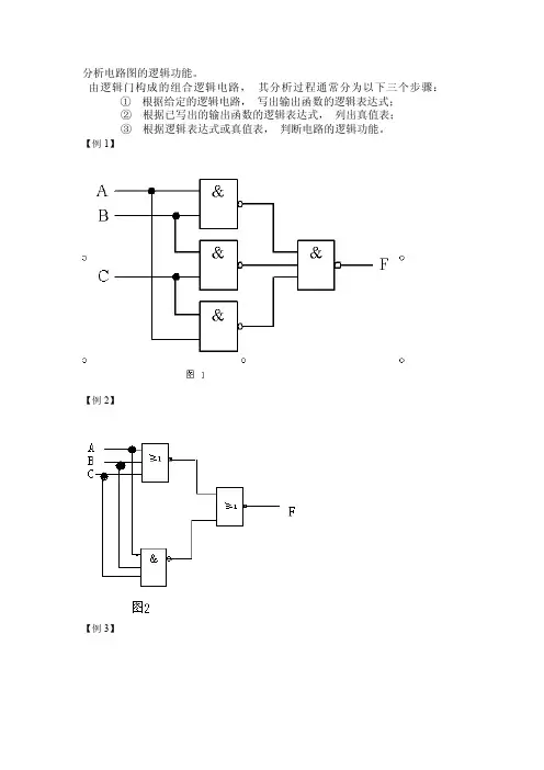
分析电路图的逻辑功能。
由逻辑门构成的组合逻辑电路,其分析过程通常分为以下三个步骤:①根据给定的逻辑电路,写出输出函数的逻辑表达式;②根据已写出的输出函数的逻辑表达式,列出真值表;③根据逻辑表达式或真值表,判断电路的逻辑功能。
【例1】【例2】【例3】【例4】组合逻辑电路的设计设计步骤: 1.逻辑问题描述将设计问题转换为逻辑问题,即用真值表或表达式的形式来描述设计问题; 2.逻辑函数化简用代数法或卡诺图法将逻辑问题化为最简与或式;3.逻辑函数变换根据给定逻辑门的类型、数量等因素,将表达式转换为所需形式; 4.画逻辑电路图并考虑实际工程问题。
【例5】设计一个组合逻辑电路,其输入ABCD 为8421BCD 码。
当输入BCD 数能被4或5整除时,电路输出F=1,否则F=0。
试分别用或非门和与或非门实现。
【例6】某厂有A 、B 、C 三个车间和Y 、 Z 两台发电机。
如果一个车间开工,启动Z 发电机即可满足使用要求; 如果两个车间同时开工,启动Y 发电机即可满足使用要求;如果三个车间同时开工,则需要同时启动Y 、 Z 两台发电机才能满足使用要求。
试仅用与非门和异或门两种逻辑门设计一个供电控制电路, 使电力负荷达到最佳匹配 【例7】.用与非门设计三变量多数表决器。
【例8】设计一个一位二进制半加器。
【例9】 用卡诺图法判断函数 是否存在险象。
触发器级电路分析D C A BD AD F ++=要确定一个用触发器构成的同步时序电路的功能,通常需要经过以下几个分析步骤:①根据给定电路写出输出方程组、激励方程组和次态方程组;②根据上述三个方程组列出电路的状态表;③根据状态表画出电路的状态图,必要时还可画出电路的工作波形;④根据状态图(或状态表、工作波形)确定电路的逻辑功能【例10】分析图5所示同步时序电路的功能,并画出电路的工作波形。
触发器级电路设计步骤(1) 导出原始状态图或状态表。
(2) 状态化简。
(3)状态分配。

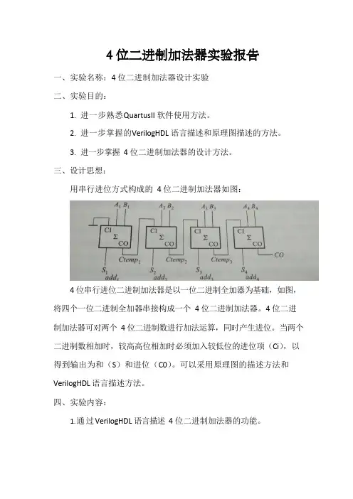
4 位二进制加法器实验报告一、实验名称:4 位二进制加法器设计实验二、实验目的:1.进一步熟悉QuartusII 软件使用方法。
2.进一步掌握的VerilogHDL 语言描述和原理图描述的方法。
3.进一步掌握4 位二进制加法器的设计方法。
三、设计思想:用串行进位方式构成的 4 位二进制加法器如图:4 位串行进位二进制加法器是以一位二进制全加器为基础,如图,将四个一位二进制全加器串接构成一个4 位二进制加法器。
4 位二进制加法器可对两个4 位二进制数进行加法运算,同时产生进位。
当两个二进制数相加时,较高高位相加时必须加入较低位的进位项(Ci),以得到输出为和(S)和进位(C0)。
可以采用原理图的描述方法和VerilogHDL 语言描述方法。
四、实验内容:1.通过VerilogHDL 语言描述4 位二进制加法器的功能。
2.通过原理图方式描述4 位二进制加法器的功能。
3.通过波形仿真验证描述4 位二进制加法器的功能。
五、实验流程:1.采用VerilogHDL 语言描述实现4 位二进制加法器:(1).首先用VerilogHDL 语言编写二进制半加器:module halfadd(s,c,a,b);input a,b;output s,c;xor(s,a,b);and(c,a,b);endmodule按周期输入波形(2).再编写一位二进制全加器:module fulladd (s,co,a,b,cl); inputa,b,cl;output s,co;wire s1,d1,d2;halfadd ha1 (s1,d1,a,b); halfadd ha2 (s,d2,s1,cl);or g1(co,d2,d1);Endmodule按周期输入波形(2).之后编写4 位二进制加法器:module bitadd (s,c3,a,b,t1);input [3:0]a,b;input t1;output [3:0]s;output c3;wire c0,c1,c2;fulladd fa0(s[0],c0,a[0],b[0],t1);fulladd fa1(s[1],c1,a[1],b[1],c0);fulladd fa2(s[2],c2,a[2],b[2],c1);fulladd fa3(s[3],c3,a[3],b[3],c2);endmodule2.按照4 位二进制加法器的工作原理可以绘制成如下原理图:3.功能仿真波形及说明:(1).按周期输入波形:由此波形图可以分析:例如0001+0001=0010、0100+0100=1000、0110+0110=1100…对于所有的两个四位二进制相加,结果正确。

贵州大学实验报告
学院:计算机科学与信息学院专业:信息安全班级:
c=1;
end
else begin //如果data_r的值不等于0000则执行以下步骤
data_r<=data_r-1; //将data_r-1的值赋给data_r
c=0;
end
end
end
end
endmodule //模块定义结束
实
验
数
据
从实验结果图可以看出当up_down=1时执行加法计数器,每当clk输入一个上升信号时计数器的值DOUT 增加1。
当up_down=0时执行减法计数器,每当clk输入一个上升信号时计数器的值DOUT减少1。
当load=1是计数器载入预留值即DOUT=DIN。
当clr输入为1是计数器执行清零操作。
注:各学院可根据教学需要对以上栏木进行增减。
表格内容可根据内容扩充。
Quartus II 74283是一种集成电路芯片,主要用于逻辑电路设计和数字信号处理。
该芯片具有高性能、稳定性好等特点,被广泛应用于数字电子产品中。
下面将详细介绍Quartus II 74283的工作原理。
一、Quartus II 74283的基本结构1. Quartus II 74283是一种四位二进制全加器,可以对四位二进制数进行加法运算。
2. 该芯片内部包含逻辑门电路、寄存器、累加器等功能模块,能够完成二进制加法运算的各个步骤。
3. Quartus II 74283采用CMOS工艺制造,具有低功耗、高集成度等特点。
二、Quartus II 74283的工作原理1. 输入端:Quartus II 74283有两个四位二进制数输入端A和B,分别用于输入要进行加法运算的两个二进制数。
2. 输出端:Quartus II 74283的输出端有一个四位二进制数输出端S,用于输出两个输入数的和。
3. 控制端:Quartus II 74283的控制端有进位输入端Cn、进位输出端Cout等,用于控制加法运算的进行。
三、Quartus II 74283的工作过程1. 初始状态:首先将要进行加法运算的两个四位二进制数分别输入到A和B端口,同时将相关的控制信号输入到控制端口。
2. 进位传递:Quartus II 74283先进行最低位的加法运算,根据A、B和Cin的输入,通过逻辑门电路判断是否需要进位,并将进位信号输出到Cout端口。
3. 两数相加:在进位传递的基础上,Quartus II 74283继续进行每一位的加法运算,直至最高位,最终输出结果到S端口。
4. 结果输出:Quartus II 74283对A、B两个输入数进行二进制加法运算后,将结果通过S端口输出,完成一次加法运算。
四、Quartus II 74283的应用领域1. Quartus II 74283广泛应用于数字电子产品中,如计算机、手机、数字电视等。
大学信息院数字电子技术根底期终考试试题〔110分钟〕(第一套)一、填空题:〔每空1分,共15分〕1.逻辑函数Y AB C=+的两种标准形式分别为〔〕、〔〕。
2.将2004个“1〞异或起来得到的结果是〔〕。
3.半导体存储器的构造主要包含三个局部,分别是〔〕、〔〕、〔〕。
4.8位转换器当输入数字量10000000为5v。
假设只有最低位为高电平,那么输出电压为〔〕v;当输入为10001000,那么输出电压为〔〕v。
5.就逐次逼近型与双积分型两种转换器而言,〔〕的抗干扰能力强,〔〕的转换速度快。
6.由555定时器构成的三种电路中,〔〕与〔〕是脉冲的整形电路。
7.及相比,器件有可编程的输出构造,它是通过对〔〕进展编程设定其〔〕的工作模式来实现的,而且由于采用了〔〕的工艺构造,可以重复编程,使它的通用性很好,使用更为方便灵活。
二、根据要求作题:〔共15分〕1.将逻辑函数写成“及或非〞表达式,并用“集电极开路及非门〞来实现。
2.图1、2中电路均由门电路构成,写出P、Q 的表达式,并画出对应A、B、C的P、Q波形。
三、分析图3所示电路:〔10分〕1)试写出8选1数据选择器的输出函数式;2)画出A2、A1、A0从000~111连续变化时,Y的波形图;3)说明电路的逻辑功能。
四、设计“一位十进制数〞的四舍五入电路〔采用8421码〕。
要求只设定一个输出,并画出用最少“及非门〞实现的逻辑电路图。
〔15分〕五、电路及、A的波形如图4(a) (b)所示,设触发器的初态均为“0〞,试画出输出端B与C的波形。
〔8分〕BC六、用T触发器与异或门构成的某种电路如图5(a)所示,在示波器上观察到波形如图5(b)所示。
试问该电路是如何连接的?请在原图上画出正确的连接图,并标明T的取值。
〔6分〕七、图6所示是16*4位与同步十六进制加法计数器74161组成的脉冲分频电路。
中的数据见表1所示。
试画出在信号连续作用下的D3、D2、D1、D0输出的电压波形,并说明它们与信号频率之比。
超前进位加法器原理74283为4位超前进位加法器,不同于普通串行进位加法器由低到高逐级进位,超前进位加法器所有位数的进位大多数情况下同时产生,运算速度快,电路结构复杂。
其管脚如图1所示:图1 74283管脚图其真值表如下所示:表1 4位超前进位加法器真值表由全加器的真值表可得Si 和Ci的逻辑表达式:定义两个中间变量Gi 和Pi:当Ai =Bi=1时,Gi=1,由Ci的表达式可得Ci=1,即产生进位,所以Gi称为产生量变。
若Pi =1,则Ai·Bi=0,Ci=Ci-1,即Pi=1时,低位的进位能传送到高位的进位输出端,故Pi称为传输变量,这两个变量都与进位信号无关。
将Gi 和Pi代入Si和Ci得:进而可得各位进位信号的逻辑表达如下:根据逻辑表达式做出电路图如下:逻辑功能图中有2输入异或门,2输入与门,3输入与门,4输入与门,2输入或门,3输入或门,4输入或门,其转化成CMOS晶体管图如下:电路网表如下:*xor 2.subckt xor2 a b c d fmxorpa 1 a vdd vdd pmos l=2 w=8 mxorpb f d 1 vdd pmos l=2 w=8 mxorpc 2 b vdd vdd pmos l=2 w=8 mxorpd f c 2 vdd pmos l=2 w=8 mxorna f a 3 0 nmos l=2 w=4 mxornb 3 b 0 0 nmos l=2 w=4 mxornc f c 4 0 nmos l=2 w=4 mxornd 4 d 0 0 nmos l=2 w=4.ends xor2*and2.subckt and2 a b fmandpa f a vdd vdd pmos l=2 w=4 mandpb f b vdd vdd pmos l=2 w=4 mandna f a 1 0 nmos l=2 w=4 mandnb 1 b 0 0 nmos l=2 w=4.ends and2*and3.subckt and3 a b c fmandpa f a vdd vdd pmos l=2 w=4 mandpb f b vdd vdd pmos l=2 w=4 mandpc f c vdd vdd pmos l=2 w=4 mandna f a 1 0 nmos l=2 w=6 mandnb 1 b 2 0 nmos l=2 w=6 mandnc 2 c 0 0 nmos l=2 w=6.ends and3*and4.subckt and4 a b c d fmandpa f a vdd vdd pmos l=2 w=4 mandpb f b vdd vdd pmos l=2 w=4 mandpc f c vdd vdd pmos l=2 w=4 mandpd f d vdd vdd pmos l=2 w=4 mandna f a 1 0 nmos l=2 w=8 mandnb 1 b 2 0 nmos l=2 w=8 mandnc 2 c 3 0 nmos l=2 w=8 mandnd 3 d 0 0 nmos l=2 w=8.ends and4*or2.subckt or2 a b fmorpa 1 a vdd vdd pmos l=2 w=8 morpb f b 1 vdd pmos l=2 w=8mna f a 0 0 nmos l=2 w=4mnb f b 0 0 nmos l=2 w=4.ends or2*or3.subckt or3 a b c fmorpa 1 a vdd vdd pmos l=2 w=12 morpb 2 b 1 vdd pmos l=2 w=12 morpc f c 2 vdd pmos l=2 w=12mna f a 0 0 nmos l=2 w=4mnb f b 0 0 nmos l=2 w=4mnc f c 0 0 nmos l=2 w=4.ends or3*or4.subckt or4 a b c d fmorpa 1 a vdd vdd pmos l=2 w=16 morpb 2 b 1 vdd pmos l=2 w=16 morpc 3 c 2 vdd pmos l=2 w=16 morpd f d 3 vdd pmos l=2 w=16mna f a 0 0 nmos l=2 w=4mnb f b 0 0 nmos l=2 w=4mnc f c 0 0 nmos l=2 w=4mnd f d 0 0 nmos l=2 w=4.ends or4*not.subckt not a fmnotpa f a vdd vdd pmos l=2 w=4 mnotna f a 0 0 nmos l=2 w=2.ends not *反相器*or21.subckt or21 a b fxor2 a b 1 or2xnot 1 f not.ends or21 *2输入或门*or31.subckt or31 a b c fxor3 a b c 1 or3xnot 1 f not.ends or31 *3输入或门*or41.subckt or41 a b c d fxor4 a b c d 1 or4xnot 1 f not.ends or41 *4输入或门*xor21.subckt xor21 a b fxm a A5 notxn b B5 notxxor a b A5 B5 f xor2.ends xor21 * 2输入异或门*and21.subckt and21 a b fxand2 a b 1 and2xnot 1 f not.ends and21 *2输入与门*and31.subckt and31 a b c fxand3 a b c 1 and3xnot 1 f not.ends and31 *3输入与门*and41.subckt and41 a b c d fxand4 a b c d 1 and4xnot 1 f not.ends and41 *4输入与门xxor211 a1 b1 p1 xor21xxor212 a2 b2 p2 xor21xxor213 a3 b3 p3 xor21xxor214 a4 b4 p4 xor21xand211 a1 b1 g1 and21xand212 a2 b2 g2 and21xand213 a3 b3 g3 and21xand214 p1 c0 m0 and21xor211 m0 g1 c1 or21 *进位C1xand311 p2 p1 c0 m1 and31xand215 p2 g1 m2 and21xor312 g2 m1 m2 c2 or31 *进位C2xand411 p3 p2 p1 c0 m3 and41xand313 p3 p2 g1 m4 and31xand216 p3 g2 m5 and21xor412 m3 m4 m5 g3 c3 or41 *进位C3xxor215 p1 c0 s1 xor21 *输出s1xxor216 p2 c1 s2 xor21 *输出s2xxor217 p3 c2 s3 xor21 *输出s3xxor218 p4 c3 s4 xor21 *输出s4.include "c:\lib\130nm_bulk.l"tt.opt scale=0.05u.global vdd gndvdd vdd 0 1.2va1 a1 0 pulse 1.2 1.2 20n 1f 1f 30n 100nva2 a2 0 pulse 0 0 20n 1f 1f 30n 100nva3 a3 0 pulse 0 0 20n 1f 1f 30n 100nva4 a4 0 pulse 0 0 20n 1f 1f 30n 100nvb1 b1 0 pulse 1.2 1.2 20n 1f 1f 30n 100n vb2 b2 0 pulse 1.2 1.2 20 1f 1f 30n 100nvb3 b3 0 pulse 0 0 20n 1f 1f 30n 100nvb4 b4 0 pulse 1.2 1.2 20n 1f 1f 30n 100nvc0 c0 0 pulse 0 0 4n 1f 1f 0n 100n.tran 1n 100n.plot tran v(s1).plot tran v(s2).plot tran v(s3).plot tran v(s4).end。
《电工与电子技术基础》课程设计报告题目四位二进制加法计数器学院(部)汽车学院专业汽车运用工程班级22020903学生姓名郭金宝学号220209031006 月12 日至06 月22 日共 1.5 周指导教师(签字)评语评审人:四位二进制加法器一.技术要求1.四位二进制加数与被加数输入2.二位显示二.摘要本设计通过逻辑开关将A3,A2,A1,A0和B3,B2,B1,B0信号作为加数和被加数输入到超前进位加法器74LS283中进行四位二进制相加,将输出信号S4,S3,S2,S1和向高位的进位C1输入一个译码器译码。
再将输出信号X4,X3,X2,X1和Y4,Y3,Y2,Y1分别输入一个74LS247型的七段显示译码器译码,最后分别接一个BS204数码管进行二位显示。
关键字:74LS283 74LS247 BS204三.总体设计方案的论证及选择1.加法器的选取加法器有两种,分别是串行进位加法器和超前进位加法器。
串行进位加法器由全加器级联构成,高位的运算必须等到低位加法完成送来进位时才能进行。
它虽然电路简单,但运算速度较慢,而且位数越多,速度就越慢。
T692型集成全加器就是这种四位串行加法器。
超前进位加法器由逻辑电路根据输入信号同时形成各位向高位的进位。
使各位的进位直接由加数和被加数来决定,而不需依赖低位进位,这就省去了进位信号逐级传送所用的时间,所以这种加法器能够快速进位。
因为它的这个优点我们选取超前进位加法器。
超前进位加法器的型号有多种,由于我们是非电专业,对电子器件的选取要求不高,为使设计简单所以选74LS283型加法器。
2.译码器的选取译码器的功能是将二进制代码(输入)按其编码时的原意翻译成对应的信号或十进制数码(输出)。
译码器是组合逻辑电路的一个重要器件,其可以分为:变量译码和显示译码两类。
译码器的种类很多,但它们的工作原理和分析设计方法大同小异,其中二进制译码器、二-十进制译码器和显示译码器是三种最典型,使用十分广泛的译码电路。