MAX5035中文资料
- 格式:pdf
- 大小:386.23 KB
- 文档页数:17
General DescriptionThe MAX5035 easy-to-use, high-efficiency, high-volt-age, step-down DC-DC converter operates from an input voltage up to 76V and consumes only 270µA qui-escent current at no load. This pulse-width modulated (PWM) converter operates at a fixed 125kHz switching frequency at heavy loads, and automatically switches to pulse-skipping mode to provide low quiescent cur-rent and high efficiency at light loads. The MAX5035includes internal frequency compensation simplifying circuit implementation. The device uses an internal low-on-resistance, high-voltage, DMOS transistor to obtain high efficiency and reduce overall system cost. This device includes undervoltage lockout, cycle-by-cycle current limit, hiccup mode output short-circuit protec-tion, and thermal shutdown.The MAX5035 delivers up to 1A output current. The out-put current may be limited by the maximum power dis-sipation capability of the package. External shutdown is included, featuring 10µA (typ) shutdown current. The MAX5035A/B/C versions have fixed output voltages of 3.3V, 5V, and 12V, respectively, while the MAX5035D features an adjustable output voltage from 1.25V to 13.2V.The MAX5035 is available in space-saving 8-pin SO and 8-pin plastic DIP packages and operates over the automotive (-40°C to +125°C) temperature range.ApplicationsAutomotiveConsumer Electronics Industrial Distributed PowerFeatures♦Wide 7.5V to 76V Input Voltage Range♦Fixed (3.3V, 5V, 12V) and Adjustable (1.25V to 13.2V) Versions ♦1A Output Current ♦Efficiency Up to 94%♦Internal 0.4ΩHigh-Side DMOS FET♦270µA Quiescent Current at No Load, 10µA Shutdown Current ♦Internal Frequency Compensation ♦Fixed 125kHz Switching Frequency♦Thermal Shutdown and Short-Circuit Current Limit ♦8-Pin SO and PDIP PackagesMAX50351A, 76V , High-Efficiency MAXPowerStep-Down DC-DC Converter________________________________________________________________Maxim Integrated Products 1Ordering Information19-2988; Rev 2; 5/04For pricing, delivery, and ordering information,please contact Maxim/Dallas Direct!at 1-888-629-4642, or visit Maxim’s website at .Pin ConfigurationTypical Operating CircuitM A X 50351A, 76V , High-Efficiency MAXPower Step-Down DC-DC ConverterABSOLUTE MAXIMUM RATINGSStresses beyond those listed under “Absolute Maximum Ratings” may cause permanent damage to the device. These are stress ratings only, and functional operation of the device at these or any other conditions beyond those indicated in the operational sections of the specifications is not implied. Exposure to absolute maximum rating conditions for extended periods may affect device reliability.(Voltages referenced to GND, unless otherwise specified.)V IN .........................................................................-0.3V to +80V SGND ....................................................................-0.3V to +0.3V LX.................................................................-0.8V to (V IN + 0.3V)BST...............................................................-0.3V to (V IN + 10V)BST (transient < 100ns)................................-0.3V to (V IN + 15V)BST to LX................................................................-0.3V to +10V BST to LX (transient < 100ns)................................-0.3V to +15V ON/OFF ........................................................-0.3V to (V IN + 0.3V)VD...........................................................................-0.3V to +12V FBMAX5035A/MAX5035B/MAX5035C...................-0.3V to +15V MAX5035D .........................................................-0.3V to +12VV OUT Short-Circuit Duration...........................................Indefinite VD Short-Circuit Duration..............................................Indefinite Continuous Power Dissipation (T A = +70°C)8-Pin PDIP (derate 9.1mW/°C above +70°C)...............727mW 8-Pin SO (derate 5.9mW/°C above +70°C)..................471mW Operating Temperature RangeMAX5035_U_ _...................................................0°C to +85°C MAX5035_A_ _..............................................-40°C to +125°C Storage Temperature Range.............................-65°C to +150°C Junction Temperature......................................................+150°C Lead Temperature (soldering, 10s).................................+300°CELECTRICAL CHARACTERISTICS (MAX5035_U_ _)(V IN = +12V, V ON/OFF = +12V, I OUT = 0, T A = 0°C to +85°C , unless otherwise noted. Typical values are at T A = +25°C. See the Typical Application Circuit.)MAX50351A, 76V , High-Efficiency MAXPowerStep-Down DC-DC ConverterELECTRICAL CHARACTERISTICS (continued) (MAX5035_U_ _)(V IN = +12V, V ON/OFF = +12V, I OUT = 0, T A = 0°C to +85°C , unless otherwise noted. Typical values are at T A = +25°C. See the Typical Application Circuit.)ELECTRICAL CHARACTERISTICS (MAX5035_A_ _)(V IN = +12V, V ON/OFF = +12V, I OUT = 0, T A = T J = -40°C to +125°C , unless otherwise noted. Typical values are at T A = +25°C. SeeM A X 50351A, 76V , High-Efficiency MAXPower Step-Down DC-DC Converter 4_______________________________________________________________________________________ELECTRICAL CHARACTERISTICS (MAX5035_A_ _)(V IN = +12V, V ON/OFF = +12V, I OUT = 0, T A = T J = -40°C to +125°C , unless otherwise noted. Typical values are at T A = +25°C. SeeNote 2:All limits at -40°C are guaranteed by design, not production tested.MAX50351A, 76V , High-Efficiency MAXPowerStep-Down DC-DC Converter_______________________________________________________________________________________5Typical Operating Characteristics(V IN = 12V, V ON/OFF = 12V, T A = -40°C to +125°C, unless otherwise noted. Typical values are at T A = +25°C. See the Typical Application Circuit , if applicable.)V OUT vs. TEMPERATURE (MAX5035AASA, V OUT = 3.3V)TEMPERATURE (°C)V O U T (V )3.243.283.323.363.403.2010050-50150-252575125V OUT vs. TEMPERATURE (MAX5035DASA, V OUT = 5V)TEMPERATURE (°C)V O U T (V )125100-252550754.854.904.955.005.055.105.155.204.80-50150LINE REGULATION(MAX5035AASA, V OUT = 3.3V)INPUT VOLTAGE (V)O U T P U T V O L T A G E (V )655035203.243.283.323.363.403.20580LINE REGULATION(MAX5035DASA, V OUT = 5V)INPUT VOLTAGE (V)O U T P U T V O L T A G E (V )655020354.854.904.955.005.055.105.155.204.80580LOAD REGULATION(MAX5035AASA, V OUT = 3.3V)I LOAD (mA)V O U T (V )8006004002003.243.283.323.363.403.201000LOAD REGULATION (MAX5035DASA, V OUT = 5V)I LOAD (mA)V O U T (V )8006004002004.955.005.055.104.901000M A X 50351A, 76V , High-Efficiency MAXPower Step-Down DC-DC Converter 6_______________________________________________________________________________________Typical Operating Characteristics (continued)(V IN = 12V, V ON/OFF = 12V, T A = -40°C to +125°C, unless otherwise noted. Typical values are at T A = +25°C. See the Typical Application Circuit , if applicable.)OUTPUT CURRENT LIMIT vs. TEMPERATURETEMPERATURE (°C)O U T P U T C U R R E N T L I M I T (A )125100755025-250.51.01.52.0-50150OUTPUT CURRENT LIMIT vs. INPUT VOLTAGEINPUT VOLTAGE (V)O U T P U T C U R R E N T L I M I T (A )655035200.81.11.41.72.00.5580QUIESCENT SUPPLY CURRENTvs. TEMPERATUREM A X 5035 t o c 12TEMPERATURE (°C)Q U I E S C E N T S U P P L Y C U R R E N T (µA )23026029032035020010050-50150-252575125QUIESCENT SUPPLY CURRENTvs. INPUT VOLTAGEINPUT VOLTAGE (V)Q U I E S C E N T S U P P L Y C U R R E N T (µA )665646362616230260290320350200676SHUTDOWN CURRENT vs. TEMPERATUREM A X 5035 t o c 14TEMPERATURE (°C)S H U T D O W N C U R R E N T (µA )5101520250100500-50150-252575125SHUTDOWN CURRENT vs. INPUT VOLTAGEINPUT VOLTAGE (V)S H U T D O W N C U R R E N T (µA )665646362616481216200676EFFICIENCY vs. LOAD CURRENT (MAX5035AASA, V OUT = 3.3V)LOAD CURRENT (mA)E F F I C I E N C Y (%)800600400200102030405060708090100001000EFFICIENCY vs. LOAD CURRENT (MAX5035DASA, V OUT = 5V)LOAD CURRENT (mA)E F F I C I E N C Y (%)800600400200102030405060708090100001000EFFICIENCY vs. LOAD CURRENT (MAX5035DASA, V OUT = 12V)LOAD CURRENT (mA)E F F I C I E N C Y (%)80060040020010203040506070809010001000MAX50351A, 76V , High-Efficiency MAXPowerStep-Down DC-DC Converter_______________________________________________________________________________________7Typical Operating Characteristics (continued)(V IN = 12V, V ON/OFF = 12V, T A = -40°C to +125°C, unless otherwise noted. Typical values are at T A = +25°C. See the Typical Application Circuit , if applicable.)OUTPUT VOLTAGE vs. INPUT VOLTAGEV IN (V)V O U T (V )1296336912150015MAX5035DASALOAD-TRANSIENT RESPONSE400µs/divBAA: V OUT , 200mV/div, AC-COUPLED B: I OUT , 500mA/div, 0.1A TO 1AV OUT = 5VMAX5035DASALOAD-TRANSIENT RESPONSEMAX5035 toc18400µs/divBAA: V OUT , 200mV/div, AC-COUPLED B: I OUT , 500mA/div, 0.5A TO 1AV OUT = 5VMAX5035DASALOAD-TRANSIENT RESPONSEMAX5035 toc19400µs/divBAA: V OUT , 200mV/div, AC-COUPLED B: I OUT , 500mA/div, 0.1A TO 0.5AV OUT = 5VMAX5035DASA LX WAVEFORMSMAX5035 toc204µs/divBA 0A: SWITCH VOLTAGE (LX PIN), 20V/div (V IN = 48V)B: INDUCTOR CURRENT, 500mA/div (I OUT = 1A)MAX5035DASA LX WAVEFORMSMAX5035 toc214µs/divB 0A 0A: SWITCH VOLTAGE (LX PIN), 20V/div (V IN = 48V)B: INDUCTOR CURRENT, 200mA/div (I OUT = 100mA)M A X 50351A, 76V , High-Efficiency MAXPower Step-Down DC-DC Converter 8_______________________________________________________________________________________Typical Operating Characteristics (continued)(V IN = 12V, V ON/OFF = 12V, T A = -40°C to +125°C, unless otherwise noted. Typical values are at T A = +25°C. See the Typical Application Circuit , if applicable.)MAX5035DASA LX WAVEFORMSMAX5035 toc224µs/divB A A: SWITCH VOLTAGE (LX PIN), 20V/div (V IN = 48V)B: INDUCTOR CURRENT, 200mA/div (I OUT = 0)00MAX5035DASA STARTUP WAVEFORM(I O = 0)MAX5035 toc231ms/divBAA: V ON/OFF , 2V/div B: V OUT , 2V/div 0MAX5035DASA STARTUP WAVEFORM(I O = 1A)MAX5035 toc241ms/divBAA: V ON/OFF , 2V/div B: V OUT , 2V/divPEAK SWITCH CURRENT LIMITvs. INPUT VOLTAGEINPUT VOLTAGE (V)P E A K S W I T C H C U R R E N T L I M I T (A )5666463626161.01.52.02.53.00.5676MAX50351A, 76V , High-Efficiency MAXPowerStep-Down DC-DC Converter_______________________________________________________________________________________9Block DiagramM A X 50351A, 76V , High-Efficiency MAXPower Step-Down DC-DC Converter 10______________________________________________________________________________________Detailed DescriptionThe MAX5035 step-down DC-DC converter operates from a 7.5V to 76V input voltage range. A unique volt-age-mode control scheme with voltage feed-forward and an internal switching DMOS FET provides high effi-ciency over a wide input voltage range. This pulse-width modulated converter operates at a fixed 125kHz switching frequency. The device also features automat-ic pulse-skipping mode to provide low quiescent cur-rent and high efficiency at light loads. Under no load,the MAX5035 consumes only 270µA, and in shutdown mode, consumes only 10µA. The MAX5035 also fea-tures undervoltage lockout, hiccup mode output short-circuit protection, and thermal shutdown.Shutdown ModeDrive ON/OFF to ground to shut down the MAX5035.Shutdown forces the internal power MOSFET off, turns off all internal circuitry, and reduces the V IN supply cur-rent to 10µA (typ). The ON/OFF rising threshold is 1.69V (typ). Before any operation begins, the voltage at ON/OFF must exceed 1.69V (typ). The ON/OFF input has 100mV hysteresis.Undervoltage Lockout (UVLO)Use the ON/OFF function to program the UVLO thresh-old at the input. Connect a resistive voltage-divider from V IN to GND with the center node to ON/OFF as shown in Figure 1. Calculate the threshold value by using the following formula:The minimum recommended V UVLO(TH)is 6.5V, 7.5V,and 13V for the output voltages of 3.3V, 5V, and 12V,respectively. The recommended value for R2 is less than 1M Ω.If the external UVLO threshold-setting divider is not used, an internal undervoltage-lockout feature monitors the supply voltage at V IN and allows operation to start when V IN rises above 5.2V (typ). This feature can be used only when V IN rise time is faster than 2ms. For slower V IN rise time, use the resistive-divider at ON/OFF .Boost High-Side Gate Drive (BST)Connect a flying bootstrap capacitor between LX and BST to provide the gate-drive voltage to the high-side N-channel DMOS switch. The capacitor is alternately charged from the internally regulated output voltage VD and placed across the high-side DMOS driver. Use a0.1µF, 16V ceramic capacitor located as close to the device as possible.On startup, an internal low-side switch connects LX to ground and charges the BST capacitor to VD. Once the BST capacitor is charged, the internal low-side switch is turned off and the BST capacitor voltage provides the necessary enhancement voltage to turn on the high-side switch.Thermal-Overload ProtectionThe MAX5035 features integrated thermal overload pro-tection. Thermal overload protection limits total power dissipation in the device, and protects the device in the event of a fault condition. When the die temperature exceeds +160°C, an internal thermal sensor signals the shutdown logic, turning off the internal power MOSFET and allowing the IC to cool. The thermal sensor turns the internal power MOSFET back on after the IC’s die tem-perature cools down to +140°C, resulting in a pulsed output under continuous thermal overload conditions.Applications InformationSetting the Output VoltageThe MAX5035A/B/C have preset output voltages of 3.3V,5.0V, and 12V, respectively. Connect FB to the preset output voltage (see the Typical Operating Circuit ).The MAX5035D offers an adjustable output voltage. Set the output voltage with a resistive voltage-divider con-nected from the circuit’s output to ground (Figure 1).Connect the center node of the divider to FB. Choose R4 less than 15k Ω, then calculate R3 as follows:Figure 1. Adjustable Output VoltageMAX5035Step-Down DC-DC Converter11The MAX5035 features internal compensation for opti-mum closed-loop bandwidth and phase margin. With the preset compensation, it is strongly advised to sense the output immediately after the primary LC.Inductor SelectionThe choice of an inductor is guided by the voltage dif-ference between V IN and V OUT , the required output current, and the operating frequency of the circuit. Use an inductor with a minimum value given by:where:I OUTMAX is the maximum output current required, and f SW is the operating frequency of 125kHz. Use an induc-tor with a maximum saturation current rating equal to at least the peak switch current limit (I LIM ). Use inductors with low DC resistance for higher efficiency.Selecting a RectifierThe MAX5035 requires an external Schottky rectifier asa freewheeling diode. Connect this rectifier close to the device using short leads and short PC board traces.Choose a rectifier with a continuous current rating greater than the highest expected output current. Use a rectifier with a voltage rating greater than the maximum expected input voltage, V IN . Use a low forward-voltage Schottky rectifier for proper operation and high efficien-cy. Avoid higher than necessary reverse-voltage Schottky rectifiers that have higher forward-voltage drops. Use a Schottky rectifier with forward-voltagedrop (V FB ) less than 0.45V at +25°C and maximum load current to avoid forward biasing of the internal body diode (LX to ground). Internal body diode conduction may cause excessive junction temperature rise and thermal shutdown. Use Table 1 to choose the proper rectifier at different input voltages and output current.Input Bypass CapacitorThe discontinuous input-current waveform of the buck converter causes large ripple currents in the input capacitor. The switching frequency, peak inductor cur-rent, and the allowable peak-to-peak voltage ripple that reflects back to the source dictate the capacitance requirement. The MAX5035 high switching frequency allows the use of smaller-value input capacitors.The input ripple is comprised of ∆V Q (caused by the capacitor discharge) and ∆V ESR (caused by the ESR of the capacitor). Use low-ESR aluminum electrolytic capacitors with high ripple-current capability at the input.Assuming that the contribution from the ESR and capaci-tor discharge is equal to 90% and 10%, respectively, cal-culate the input capacitance and the ESR required for a specified ripple using the following equations:I OUT is the maximum output current of the converter and f SW is the oscillator switching frequency (125kHz).For example, at V IN = 48V, V OUT = 3.3V, the ESR and input capacitance are calculated for the input peak-to-peak ripple of 100mV or less yielding an ESR and capacitance value of 80m Ωand 51µF, respectively.Low-ESR, ceramic, multilayer chip capacitors are recom-mended for size-optimized application. For ceramic capacitors, assume the contribution from ESR and capaci-tor discharge is equal to 10% and 90%, respectively.The input capacitor must handle the RMS ripple current without significant rise in temperature. The maximum capacitor RMS current occurs at about 50% duty cycle.ESR V I I IN ESR OUT L =+∆∆2M A X 5035Step-Down DC-DC Converter 12______________________________________________________________________________________Ensure that the ripple specification of the input capaci-tor exceeds the worst-case capacitor RMS ripple cur-rent. Use the following equations to calculate the input capacitor RMS current:I PRMS is the input switch RMS current, I AVGIN is the input average current, and ηis the converter efficiency.The ESR of aluminum electrolytic capacitors increases significantly at cold temperatures. Use a 1µF or greater value ceramic capacitor in parallel with the aluminum electrolytic input capacitor, especially for input voltages below 8V.Output Filter CapacitorThe worst-case peak-to-peak and RMS capacitor ripple current, allowable peak-to-peak output ripple voltage,and the maximum deviation of the output voltage dur-ing load steps determine the capacitance and the ESR requirements for the output capacitors.The output capacitance and its ESR form a zero, which improves the closed-loop stability of the buck regulator.Choose the output capacitor so the ESR zero frequency (f Z ) occurs between 20kHz to 40kHz. Use the following equation to verify the value of f Z . Capacitors with 100m Ωto 250m ΩESR are recommended to ensure the closed-loop stability, while keeping the output ripple low.The output ripple is comprised of ∆V OQ (caused by the capacitor discharge) and ∆V OESR (caused by the ESR of the capacitor). Use low-ESR tantalum or aluminum electrolytic capacitors at the output. Assuming that the contributions from the ESR and capacitor discharge equal 80% and 20% respectively, calculate the outputcapacitance and the ESR required for a specified rip-ple using the following equations:The MAX5035 has an internal soft-start time (t SS ) of 400µs. It is important to keep the output rise time at startup below t SS to avoid output overshoot. The output rise time is directly proportional to the output e 68µF or lower capacitance at the output to control the overshoot below 5%.In a dynamic load application, the allowable deviation of the output voltage during the fast-transient load dic-tates the output capacitance value and the ESR. The output capacitors supply the step load current until the controller responds with a greater duty cycle. The response time (t RESPONSE ) depends on the closed-loop bandwidth of the converter. The resistive drop across the capacitor ESR and capacitor discharge cause a voltage droop during a step load. Use a com-bination of low-ESR tantalum and ceramic capacitors for better transient load and ripple/noise performance.Keep the maximum output-voltage deviation above the tolerable limits of the electronics being powered.Assuming a 50% contribution each from the output capacitance discharge and the ESR drop, use the fol-lowing equations to calculate the required ESR and capacitance value:where I STEP is the load step and t RESPONSE is the response time of the controller. Controller response time is approximately one-third of the reciprocal of the closed-loop unity-gain bandwidth, 20kHz typically.PC Board Layout ConsiderationsProper PC board layout is essential. Minimize ground noise by connecting the anode of the Schottky rectifier,the input bypass capacitor ground lead, and the output filter capacitor ground lead to a single point (“star”MAX5035Step-Down DC-DC Converter______________________________________________________________________________________13ground configuration). A ground plane is required.Minimize lead lengths to reduce stray capacitance,trace resistance, and radiated noise. In particular,place the Schottky rectifier diode right next to thedevice. Also, place BST and VD bypass capacitors very close to the device. Use the PC board copper plane connecting to V IN and LX for heatsinking.Figure 2. Fixed Output VoltagesApplication CircuitsM A X 5035Step-Down DC-DC Converter 14______________________________________________________________________________________MAX5035Step-Down DC-DC Converter______________________________________________________________________________________15Figure 3. Load Temperature Monitoring with ON/OFF (Requires Accurate V IN )M A X 5035Step-Down DC-DC Converter 16______________________________________________________________________________________Figure 4. Dual-Sequenced DC-DC Converters (Startup Delay Determined by R1/R1’, Ct/Ct’ and Rt/Rt’)Chip InformationTRANSISTOR COUNT: 4344PROCESS: BiCMOSMAX5035Step-Down DC-DC Converter______________________________________________________________________________________17Package Information(The package drawing(s) in this data sheet may not reflect the most current specifications. For the latest package outline information,go to /packages .)M A X 5035Step-Down DC-DC Converter Maxim cannot assume responsibility for use of any circuitry other than circuitry entirely embodied in a Maxim product. No circuit patent licenses are implied. Maxim reserves the right to change the circuitry and specifications without notice at any time.18____________________Maxim Integrated Products, 120 San Gabriel Drive, Sunnyvale, CA 94086 408-737-7600©2004 Maxim Integrated ProductsPrinted USAis a registered trademark of Maxim Integrated Products.Package Information (continued)(The package drawing(s) in this data sheet may not reflect the most current specifications. For the latest package outline information,go to /packages .)。
本文是Maxim 正式英文资料的译文,Maxim 不对翻译中存在的差异或由此产生的错误负责。
请注意译文中可能存在文字组织或翻译错误,如需确认任何词语的准确性,请参考Maxim 提供的英文版资料。
索取免费样品和最新版的数据资料,请访问Maxim 的主页: 。
_______________________________概述MAX481、MAX483、MAX485、MAX487-MAX491以及MAX1487是用于RS-485与RS-422通信的低功耗收发器,每个器件中都具有一个驱动器和一个接收器。
MAX483、MAX487、MAX488以及MAX489具有限摆率驱动器,可以减小EMI ,并降低由不恰当的终端匹配电缆引起的反射,实现最高250k b p s 的无差错数据传输。
M A X 481、MAX485、MAX490、MAX491、MAX1487的驱动器摆率不受限制,可以实现最高2.5Mbps 的传输速率。
这些收发器在驱动器禁用的空载或满载状态下,吸取的电源电流在120(A 至500(A 之间。
另外,MAX481、MAX483与MAX487具有低电流关断模式,仅消耗0.1µA 。
所有器件都工作在5V 单电源下。
驱动器具有短路电流限制,并可以通过热关断电路将驱动器输出置为高阻状态,防止过度的功率损耗。
接收器输入具有失效保护特性,当输入开路时,可以确保逻辑高电平输出。
MAX487与MAX1487具有四分之一单位负载的接收器输入阻抗,使得总线上最多可以有128个M A X 487/MAX1487收发器。
使用MAX488-MAX491可以实现全双工通信,而MAX481、MAX483、MAX485、MAX487与MAX1487则为半双工应用设计。
_______________________________应用低功耗RS-485收发器低功耗RS-422收发器电平转换器用于EMI 敏感应用的收发器工业控制局域网____________________下一代器件的特性♦容错应用MAX3430: ±80V 故障保护、失效保护、1/4单位负载、+3.3V 、RS-485收发器MAX3440E-MAX3444E: ±15kV ESD 保护、±60V 故障保护、10Mbps 、失效保护、RS-485/J1708收发器♦对于空间受限应用MAX3460-MAX3464: +5V 、失效保护、20Mbps 、Profibus RS-485/RS-422收发器MAX3362: +3.3V 、高速、RS-485/RS-422收发器,采用SOT23封装MAX3280E-MAX3284E: ±15kV ESD 保护、52Mbps 、+3V 至+5.5V 、SOT23、RS-485/RS-422、真失效保护接收器MAX3293/MAX3294/MAX3295: 20Mbps 、+3.3V 、SOT23、RS-485/RS-422发送器♦对于多通道收发器应用MAX3030E-MAX3033E: ±15kV ESD 保护、+3.3V 、四路RS-422发送器♦对于失效保护应用MAX3080-MAX3089: 失效保护、高速(10Mbps)、限摆率RS-485/RS-422收发器♦对于低电压应用MAX3483E/MAX3485E/MAX3486E/MAX3488E/MAX3490E/MAX3491E: +3.3V 供电、±15kV ESD 保护、12Mbps 、限摆率、真正的RS-485/RS-422收发器MAX481/MAX483/MAX485/MAX487–MAX491/MAX1487低功耗、限摆率、RS-485/RS-422收发器_____________________________________________________________________选择表19-0122; Rev 8; 10/03定购信息在本资料的最后给出。
General DescriptionThe MAX6012/MAX6021/MAX6025/MAX6030/MAX6041/MAX6045/MAX6050 precision, low-dropout, micropower voltage references are available in miniature SOT23-3surface-mount packages. They feature a proprietary curvature-correction circuit and laser-trimmed thin-film resistors that result in a low temperature coefficient of <15ppm/°C and initial accuracy of better than 0.2%.These devices are specified over the extended temper-ature range.These series-mode voltage references draw only 27µA of quiescent supply current and can sink or source up to 500µA of load current. Unlike conventional shunt-mode (two-terminal) references that waste supply cur-rent and require an external resistor, devices in the MAX6012family offer a supply current that’s virtually independent of supply voltage (with only a 0.8µA/V vari-ation with supply voltage) and do not require an external resistor. Additionally, these internally compensated devices do not require an external compensation capacitor and are stable with up to 2.2nF of load capac-itance. Eliminating the external compensation capacitor saves valuable board area in space-critical applications.Their low dropout voltage and supply-independent,ultra-low supply current make these devices ideal for battery-operated, low-voltage systems.ApplicationsHand-Held Equipment Data Acquisition SystemsIndustrial and Process-Control Systems Battery-Operated Equipment Hard-Disk DrivesFeatureso 0.2% (max) Initial Accuracyo 15ppm/°C (max) Temperature Coefficient o 35µA (max) Quiescent Supply Current o 0.8µA/V Supply Current Variation with V IN o ±500µA Output Source and Sink Current o 100mV Dropout at 500µA Load Current o 0.12µV/µA Load Regulation o 8µV/V Line Regulationo Stable with C LOAD = 0 to 2.2nFMAX6012/6021/6025/6030/6041/6045/6050Precision, Low-Power, Low-Dropout,SOT23-3 Voltage References________________________________________________________________Maxim Integrated Products 1Typical Operating Circuit19-4777; Rev 3; 4/01Ordering InformationPin Configuration appears at end of data sheet.Selector GuideFor price, delivery, and to place orders,please contact Maxim Distribution at 1-888-629-4642,or visit Maxim’s website at .M A X 6012/6021/6025/6030/6041/6045/6050Precision, Low-Power, Low-Dropout, SOT23-3 Voltage References 2_______________________________________________________________________________________ABSOLUTE MAXIMUM RATINGSELECTRICAL CHARACTERISTICS—MAX6012(V IN = +5V, I OUT = 0, T A = T MIN to T MAX , unless otherwise noted. Typical values are at T A = +25°C.) (Note 1)Stresses beyond those listed under “Absolute Maximum Ratings” may cause permanent damage to the device. These are stress ratings only, and functional operation of the device at these or any other conditions beyond those indicated in the operational sections of the specifications is not implied. Exposure to absolute maximum rating conditions for extended periods may affect device reliability.(Voltages Referenced to GND)IN.........................................................................-0.3V to +13.5V OUT .............................................................-0.3V to (V IN + 0.3V)Output Short Circuit to GND or IN (V IN < 6V)............Continuous Output Short Circuit to GND or IN (V IN ≥6V).........................60sContinuous Power Dissipation (T A = +70°C)3-Pin SOT23-3 (derate 4.0mW/°C above +70°C)........320mW Operating Temperature Range ...........................-40°C to +85°C Storage Temperature Range.............................-65°C to +150°C Lead Temperature (soldering, 10s).................................+300°CELECTRICAL CHARACTERISTICS—MAX6021MAX6012/6021/6025/6030/6041/6045/6050Precision, Low-Power, Low-Dropout, SOT23-3 Voltage References(V IN= +5V, I OUT= 0, T A= T MIN to T MAX, unless otherwise noted. Typical values are at T A= +25°C.) (Note 1)M A X 6012/6021/6025/6030/6041/6045/6050Precision, Low-Power, Low-Dropout, SOT23-3 Voltage References 4_______________________________________________________________________________________ELECTRICAL CHARACTERISTICS—MAX6025(V IN = +5V, I OUT = 0, T A = T MIN to T MAX , unless otherwise noted. Typical values are at T A = +25°C.) (Note 1)ELECTRICAL CHARACTERISTICS—MAX6030MAX6012/6021/6025/6030/6041/6045/6050Precision, Low-Power, Low-Dropout, SOT23-3 Voltage References(V IN= +5V, I OUT= 0, T A= T MIN to T MAX, unless otherwise noted. Typical values are at T A= +25°C.) (Note 1) Array_______________________________________________________________________________________5M A X 6012/6021/6025/6030/6041/6045/6050Precision, Low-Power, Low-Dropout, SOT23-3 Voltage References 6_______________________________________________________________________________________ELECTRICAL CHARACTERISTICS—MAX6041(V IN = +5V, I OUT = 0, T A = T MIN to T MAX , unless otherwise noted. Typical values are at T A = +25°C.) (Note 1)ELECTRICAL CHARACTERISTICS—MAX6045MAX6012/6021/6025/6030/6041/6045/6050Precision, Low-Power, Low-Dropout, SOT23-3 Voltage References(V IN= +5V, I OUT= 0, T A= T MIN to T MAX, unless otherwise noted. Typical values are at T A= +25°C.) (Note 1)M A X 6012/6021/6025/6030/6041/6045/6050Precision, Low-Power, Low-Dropout, SOT23-3 Voltage References 8_______________________________________________________________________________________Note 1:All devices are 100% production tested at T A = +25°C and are guaranteed by design for T A = T MIN to T MAX , as specified.Note 2:Temperature Coefficient is measured by the “box” method, i.e., the maximum ∆V OUT is divided by the maximum ∆t.Note 3:Temperature Hysteresis is defined as the change in +25°C output voltage before and after cycling the device from T MIN to T MAX .Note 4:Not production tested. Guaranteed by design.Note 5:Dropout voltage is the minimum input voltage at which V OUT changes ≤0.2% from V OUT at V IN = 5.0V (V IN = 5.5V for MAX6050).ELECTRICAL CHARACTERISTICS—MAX6050(V IN = +5.5V, I OUT = 0, T A = T MIN to T MAX , unless otherwise noted. Typical values are at T A = +25°C.) (Note 1)MAX6012/6021/6025/6030/6041/6045/6050Precision, Low-Power, Low-Dropout,SOT23-3 Voltage References_______________________________________________________________________________________9Typical Operating Characteristics(V IN = +5V for MAX6012/21/25/30/41/45, V IN = +5.5V for MAX6050; I OUT = 0; T A = +25°C; unless otherwise noted.) (Note 6)1.24701.24801.24751.24901.24851.25051.25001.24951.2510-40-2020406080100MAX6012OUTPUT VOLTAGE TEMPERATURE DRIFTTEMPERATURE DRIFT (°C)V O U T (V )4.9864.9904.9884.9964.9944.9925.0025.0004.9985.004-4020-20406080100MAX6050OUTPUT VOLTAGE TEMPERATURE DRIFTTEMPERATURE DRIFT (°C)V O U T (V ) 4.9934.9954.9944.9994.9984.9974.9965.0025.0015.0005.00303004005001002006007008009001000MAX6050LONG-TERM DRIFTTIME (h)O U T P U T V O L T A G E (V )-1002001003004002648101214MAX6012LINE REGULATIONINPUT VOLTAGE (V)O U T P U T V O L T A G E C H A N G E (µV )-0.4-0.20.20.4-500-2500250-375-125125375500MAX6012LOAD REGULATIONLOAD CURRENT (µA)O U T P U T V O L T A G E C H A N G E (m V )-2004002006008005791113MAX6050LINE REGULATIONINPUT VOLTAGE (V)O U T P U T V O L T A G E C H A N G E (µV )0.10.20.30.40.50.60.70.802004006008001000MAX6025/MAX6030DROPOUT VOLTAGE vs.SOURCE CURRENTSOURCE CURRENT (µA)D R O P O U T V O L T A GE (V )-0.400-0.2000.2000.400-500-2500250-375-125125375500MAX6050LOAD REGULATIONLOAD CURRENT (µA)O U T P U T V O L T A G E C H A N G E (m V )0.100.050.200.150.250.3004002006008001000MAX6041/MAX6045/MAX6050DROPOUT VOLTAGE vs.SOURCE CURRENTSOURCE CURRENT (µA)D R O P O U T V O L T A GE (V )M A X 6012/6021/6025/6030/6041/6045/6050Precision, Low-Power, Low-Dropout, SOT23-3 Voltage References 10______________________________________________________________________________________1001k10k100k1M10MMAX6012POWER-SUPPLY REJECTIONvs. FREQUENCYM A X 6012-10FREQUENCY (Hz)P S R (m V /V )1000.010.1110MAX6050POWER-SUPPLY REJECTIONvs. FREQUENCYFREQUENCY (Hz)P S R (m V /V )1000.010.11101010k100k1M1001k10M20262422283032343638402648101214SUPPLY CURRENT vs. INPUT VOLTAGEINPUT VOLTAGE (V)S U P P L Y C U R R E N T (µA )0.0110010k 10.1101k100k 1MMAX6012OUTPUT IMPEDANCE vs. FREQUENCYM A X 6012-13FREQUENCY (Hz)O U T P U T I M P E D A N C E (Ω)0.11101001k 0.0110010k 10.1101k100k 1MMAX6050OUTPUT IMPEDANCE vs. FREQUENCYM A X 6012-14FREQUENCY (Hz)O U T P U T I M P E D A N C E (Ω)0.11101001k 2025303540SUPPLY CURRENT vs. TEMPERATURETEMPERATURE (°C)S U P P L Y C U R R E N T (µA )-402040-206080100V OUT 20µV/div1sec/div MAX60500.1Hz TO 10Hz OUTPUT NOISEM A X 6012-17V IN 1V/divV OUT 1V/div10µs/divMAX6012TURN-ON TRANSIENTM A X 6012-18Typical Operating Characteristics (continued)(V IN = +5V for MAX6012/21/25/30/41/45, V IN = +5.5V for MAX6050; I OUT = 0; T A = +25°C; unless otherwise noted.) (Note 6)V OUT 10µV/div1sec/div MAX60120.1Hz TO 10Hz OUTPUT NOISEM A X 6012-16MAX6012/6021/6025/6030/6041/6045/6050Precision, Low-Power, Low-Dropout,SOT23-3 Voltage References______________________________________________________________________________________11Typical Operating Characteristics (continued)(V IN = +5V for MAX6012/21/25/30/41/45, V IN = +5.5V for MAX6050; I OUT = 0; T A = +25°C; unless otherwise noted.) (Note 6)I OUT 40µA/div+25µA-25µAV OUT 20mV/div10µs/divMAX6012LOAD-TRANSIENT RESPONSEMAX6012-19I OUT = ±25µA, AC-COUPLEDI OUT 50µA/divV OUT 50mV/div20µs/divMAX6050LOAD-TRANSIENT RESPONSEM A X 6012-20V IN = 5.5V, I OUT = ±25µA, AC-COUPLEDV IN 2V/divV OUT 2V/div10µs/divMAX6050TURN-ON TRANSIENTM A X 6012-21+500µA-500µA V OUT 0.2V/divI OUT 1mA/div10µs/divMAX6012LOAD-TRANSIENT RESPONSEMAX6012-22I OUT = ±500µA, AC-COUPLEDV IN200mV/divV OUT 100mV/div2µs/divV IN = 5.5V ±0.25V, AC-COUPLEDMAX6050LINE-TRANSIENT RESPONSEM A X 6012-25I OUT500µA/divV OUT 200mV/div20µs/divMAX6050LOAD-TRANSIENT RESPONSEM A X 6012-23V IN = 5.5V, I OUT = ±500µA, AC-COUPLED V IN200mV/divV OUT 100mV/div2.5µs/divV IN = 5V ±0.25V, AC-COUPLEDMAX6012LINE-TRANSIENT RESPONSEM A X 6012-24Note 6:Many of the Typical Operating Characteristics of the MAX6012 family areextremely similar. The extremes of these characteristics are found in the MAX6012 (1.2V output) and the MAX6050 (5.0V output). The TypicalOperating Characteristics of the remainder of the MAX6012 family typically lie between these two extremes and can be estimated based on their output voltage.M A X 6012/6021/6025/6030/6041/6045/6050Precision, Low-Power, Low-Dropout, SOT23-3 Voltage References 12______________________________________________________________________________________Detailed DescriptionThe MAX6012/MAX6021/MAX6025/MAX6030/MAX6041/MAX6045/MAX6050 precision bandgap references use a proprietary curvature-correction circuit and laser-trimmed thin-film resistors, resulting in a low tempera-ture coefficient of <20ppm/°C and initial accuracy of better than 0.2%. These devices can sink and source up to 500µA with <200mV of dropout voltage, making them attractive for use in low-voltage applications.Applications InformationOutput/Load CapacitanceDevices in this family do not require an output capaci-tance for frequency stability. They are stable for capac-itive loads from 0 to 2.2nF. H owever, in applications where the load or the supply can experience step changes, an output capacitor will reduce the amount of overshoot (or undershoot) and assist the circuit’s tran-sient response. Many applications do not need an external capacitor, and this family can offer a signifi-cant advantage in these applications when board space is critical.Supply CurrentThe quiescent supply current of these series-mode ref-erences is a maximum of 35µA and is virtually indepen-dent of the supply voltage, with only a 0.8µA/V variation with supply voltage. Unlike series references, shunt-mode references operate with a series resistor con-nected to the power supply. The quiescent current of a shunt-mode reference is thus a function of the input voltage. Additionally, shunt-mode references have to be biased at the maximum expected load current, even if the load current is not present all the time. The load current is drawn from the input voltage only when required, so supply current is not wasted and efficiency is maximized at all input voltages. This improved effi-ciency can help reduce power dissipation and extend battery life.When the supply voltage is below the minimum speci-fied input voltage (as during turn-on), the devices can draw up to 200µA beyond the nominal supply current.The input voltage source must be capable of providing this current to ensure reliable turn-on.Output Voltage HysteresisOutput voltage hysteresis is the change in the output voltage at T A = +25°C before and after the device is cycled over its entire operating temperature range.H ysteresis is caused by differential package stress appearing across the bandgap core transistors. The typical temperature hysteresis value is 130ppm.Figure 1. Positive and Negative References from Single +3V or +5V SupplyMAX6012/6021/6025/6030/6041/6045/6050Precision, Low-Power, Low-Dropout,SOT23-3 Voltage References______________________________________________________________________________________13Pin ConfigurationChip InformationTRANSISTOR COUNT: 70Turn-On TimeThese devices typically turn on and settle to within 0.1% of their final value; 30µs to 220µs depending on the device. The turn-on time can increase up to 1.5ms with the device operating at the minimum dropout volt-age and the maximum load.Positive and Negative Low-PowerVoltage ReferenceFigure 1 shows a typical method for developing a bipo-lar reference. The circuit uses a MAX681 voltage dou-bler/inverter charge-pump converter to power an ICL7652, thus creating a positive as well as a negative reference voltage.M A X 6012/6021/6025/6030/6041/6045/6050Precision, Low-Power, Low-Dropout, SOT23-3 Voltage ReferencesPackage Information。

1/25 使用之前注意事项 SMA 接头输入信号绝不能有直流成分!否则,必须采用直流隔离器。
SMA 接头输入信号电压不允许超过 200mV! 仪器工作环境温度:0°C - 40°C。
仪器工作环境相对湿度:小于 85%。
仪器和微机相连的 USB 电缆必须具有消除电磁干扰的措施。
AC-DC 电源: AC 输入: 50Hz , 100-240V,0.4A; DC 输出: 12V, 0.75A,Φ3.5mm 插头,内正外负。
给机内电池充电前,切记把插头 全 部 插 入 插 孔,避免充不上电! 为了运输安全,新仪器中电池只充了一点电。
新的标配 1300mAh 电池充满约需 24 小时,新的选配 3000mAh 电池充满约需 45 小时左右。
其余操作事项以及说明参见用户手册(英文)。
既有 HF-60105 又有 NF-5035 的用户,建议先看 NF-5035 操作手册。
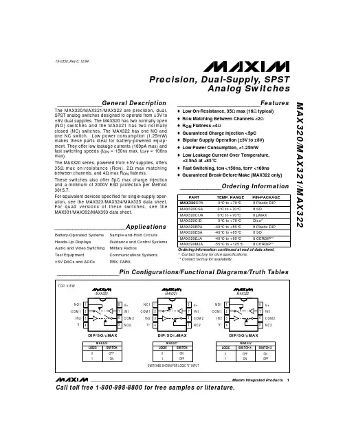
2/25 NF-5035 频谱分析仪 DC 电源插口 耳机插口 转盘SMA 接头 外接探头 或者信号USB 插口不同测量 任务需要 用户给频 谱仪设置 不同参数通过面板操作键 以及显示屏菜单 设 置 参 数3/25 频谱仪操作键连接微机 USB 插口转 盘数字键 或热键点键Shift 电源开关 回车 清零 或 启动工频磁场测试 导航 菜单 各 种 操 作 键 NF-5035 有三种工作模式: 频 谱 分 析、 暴 露 限 值、 音 频 解 调。
General DescriptionThe MAX1556 evaluation kit (EV kit) is a fully assembled and tested circuit board that evaluates the MAX1556and MAX1557 PWM step-down DC-DC converters. The circuit operates from 2.6V to 5.5V. The MAX1556 deliv-ers up to 1.2A and has pin-selectable 1.8V, 2.5V, 3.3V,and adjustable output. The MAX1557 delivers up to 600mA and has pin-selectable 1V, 1.3V, 1.5V, and adjustable output. Each circuit features an on-board shutdown control.Features♦Up to 97% Efficiency♦95% Efficiency at 1mA Load Current ♦1MHz PWM Switching Frequency ♦Tiny Inductors♦Pin-Selectable Output VoltagesMAX1556: 3.3V, 2.5V, 1.8V, and Adjustable MAX1557: 1.5V, 1.3V, 1.0V, and Adjustable ♦1.2A Guaranteed Output Current (MAX1556)♦Voltage Positioning Optimizes Load-Transient Response ♦Low 16µA Quiescent Current♦Low 27µA Quiescent Current in Dropout ♦Low 0.1µA Shutdown Current♦Analog Soft-Start with Zero Overshoot Current ♦Small, 10-Pin, 3mm x 3mm TDFN Package ♦Fully Assembled and TestedEvaluates: MAX1556/MAX1557MAX1556 Evaluation KitMaxim Integrated Products 119-3415; Rev 0; 9/04For pricing, delivery, and ordering information,please contact Maxim/Dallas Direct!at 1-888-629-4642, or visit Maxim’s website at .Ordering InformationComponent SuppliersNote:Indicate that you are using the MAX1556 when contacting these component suppliers.*EP = Exposed paddle.Quick StartRecommended Equipment•One variable DC power supply capable of supply-ing up to 5.5V at 1.2A •One voltmeter (DMM)Procedure (MAX1556ETB)The MAX1556 EV kit is fully assembled and tested.Follow the steps below to verify board operation:1)Select the desired output voltage with JU1, JU2,and JU3 (see Table 1). The EV kit is preset to a 1.8V output.2)Connect the positive terminal of the voltmeter to thepad labeled OUT. Connect the ground terminal of the voltmeter to the pad labeled GND nearest the OUT pad. Connect a load from OUT to the GND pad closest to OUT.3)Preset the power supply to between 2.6V and 5.5V,and turn the power supply off. Do not turn on the power supply until all connections are completed.4)Connect the positive power-supply terminal to thepad labeled IN. Connect the power-supply ground to the pad labeled GND nearest the IN pad.5)Turn on the power supply and verify the output volt-age is the desired voltage from setting JU1, JU2,and JU3 (default is 1.8V).Procedure (MAX1557ETB)The MAX1556 EV kit is fully assembled and tested.Follow the steps below to verify board operation:1)Select the desired output voltage with JU4, JU5,and JU6 (see Table 2). The EV kit is preset to a 1.0V output.2)Connect the positive terminal of the voltmeter to thepad labeled OUT2. Connect the ground terminal of the voltmeter to the pad labeled GND2 nearest the OUT2 pad. Connect a load from OUT2 to the GND2pad closest to OUT2.3)Preset the power supply to between 2.6V and 5.5V,and turn the power supply off. Do not turn on the power supply until all connections are completed.4)Connect the positive power-supply terminal to thepad labeled IN2. Connect the power-supply ground to the pad labeled GND2 nearest the IN2 pad.5)Turn on the power supply and verify the output volt-age is the desired voltage from setting JU4, JU5,and JU6 (default is 1.0V).Detailed DescriptionThe MAX1556 EV kit contains two separate PWM step-down DC-DC converter circuits. Either circuit can be powered from a DC power supply with a 2.6V to 5.5V input range. The top and bottom circuit are separate from each other and do not share a common ground plane.The top circuit (MAX1556) provides pin-selectable out-put voltages of 3.3V, 2.5V, 1.8V, and adjustable at 1.2A.The bottom circuit (MAX1557) provides pin-selectable output voltages of 1.5V, 1.3V, 1.0V, and adjustable at 600mA.Pin-Selectable Output VoltagesThe MAX1556 output voltage is selected with JU1 and JU2, as shown in Table 1.The MAX1557 output voltage is selected with JU4 and JU5, as shown in Table 2.Evaluating Other Output VoltagesThe MAX1556 EV kit comes with the MAX1556 preset to a 1.8V output and the MAX1557 preset to a 1V output.To evaluate other voltages besides the preset values,set the MAX1556 (or MAX1557) to adjustable mode.The footprints for the feedback resistors are available on the backside of the evaluation kit. Refer to the Adjusting the O utput Voltage section in the MAX1556data sheet for a detailed description on calculating these feedback resistor values for the desired output voltage. Resistor R1 for the MAX1556 circuit (R3 on MAX1557) is shorted on the evaluation kit. This short must be cut prior to the placement of a resistor on the footprint. Resistor R2 for the MAX1556 circuit (R4 for MAX1557) is open and requires no modification before placing a resistor on the footprint.E v a l u a t e s : M A X 1556/M A X 1557MAX1556 Evaluation Kit 2_______________________________________________________________________________________Table 1. Output Voltage Selection (MAX1556ETB)Note: Default configuration is JU1, JU2, and JU3 (1 and 2).External Shutdown ControlThe MAX1556 EV kit comes preset with SHDN and SHDN2pulled high so that the MAX1556 and MAX1557are enabled when the input voltage is applied. To operate the shutdown control from an external signal, remove the shunt on JU3 for the MAX1556 (JU6 for the MAX1557).Apply a logic high to SHDN to enable the MAX1556, or apply a logic low to shut down the MAX1556. Apply a logic high to SHDN2to enable the MAX1557, or apply a logic low to shut down the MAX1557.Evaluates: MAX1556/MAX1557MAX1556 Evaluation Kit_______________________________________________________________________________________3Table 2. Output Voltage Selection (MAX1557ETB)Note:Default configuration is JU4, JU5, and JU6 (1 and 2).Figure 1a. MAX1556 EV Kit Schematic (MAX1556)E v a l u a t e s : M A X 1556/M A X 1557MAX1556 Evaluation Kit 4_______________________________________________________________________________________Evaluates: MAX1556/MAX1557MAX1556 Evaluation Kit_______________________________________________________________________________________5Figure 2. MAX1556 EV Kit Component Placement Guide—Component SideFigure 3. MAX1556 EV Kit Component Placement Guide—Solder SideMaxim cannot assume responsibility for use of any circuitry other than circuitry entirely embodied in a Maxim product. No circuit patent licenses are implied. Maxim reserves the right to change the circuitry and specifications without notice at any time.6_____________________Maxim Integrated Products, 120 San Gabriel Drive, Sunnyvale, CA 94086 408-737-7600©2004 Maxim Integrated ProductsPrinted USAis a registered trademark of Maxim Integrated Products.E v a l u a t e s : M A X 1556/M A X 1557MAX1556 Evaluation KitFigure 4. MAX1556 EV Kit PC Board Layout—Component SideFigure 5. MAX1556 EV Kit PC Board Layout—Solder Side。
汽车LED灯驱动电路LED灯电源决定了LED灯的使用寿命。
散热和光的方向性是LED照明中首要考虑的问题。
采用多个小电流的LED串、并联组成阵列的方案可有效解决散热问题,同时改善LED照明中光的方向性;而且目前小电流芯片的光效率要高于大功率LED 芯片。
1. LED的恒流源驱动方式恒流源驱动是最佳的LED驱动方式,采用恒流源驱动,不用在输出电路串联限流电阻,LED上流过的电流也不受外界电源电压变化、环境温度变化,以及LED参数离散性的影响,从而能坚持电流恒定,充分发挥LED的各种优异特性。
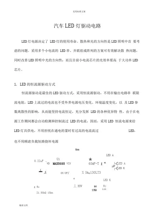
由于在电源工作期间都会自动检测和控制流过LED的电流,因而,采用LED 恒流电源来给LED灯具供电,不用担忧在通电的霎时有过高的电流流过LED,也不用顾虑负载短路烧坏电源UrnLED A0.22uF 、VDU1MAX5035 VINON/OFI'g Rs21.50kQ 10kn★68M F-T I 01X5B RS13OLT3+丄35V R415QLED KRjisnLED ALED K错误!未找到引用源图1是用于汽车转向灯的高亮度LED电源原理图。
它采用固定频率、高集成度脉宽调制PWM开关转换器MAX5035,输出电流可达1 A。
基于电感的buck调节器能够准确控制流过LED (或几个串联LED,总电压为12 V)的电流,MAX5035的开关频率为125 kHz,输入电压高达76 V (须使用更高额定电压的输入电容和二极管)。
通过调节控制电压(0~3.9 V),MAX5035 LED 电流驱动器能够在LED_A和LED_K端产生近似350~0mA的输出电流。
此电路可以在较宽的输入电压范围内控制并保持恒定的LED电流。
该电路的设计参数为:最小输入电压7.5V (大多单个LED),最大输入电压30V (受D1和C8、C9限制),最大输出电流350mA (U conte =0),最大输出电压12V (由MAX5035内部限制,电流350mA),控制电压范围U control为0V (满电流)至3.9V (全暗)。
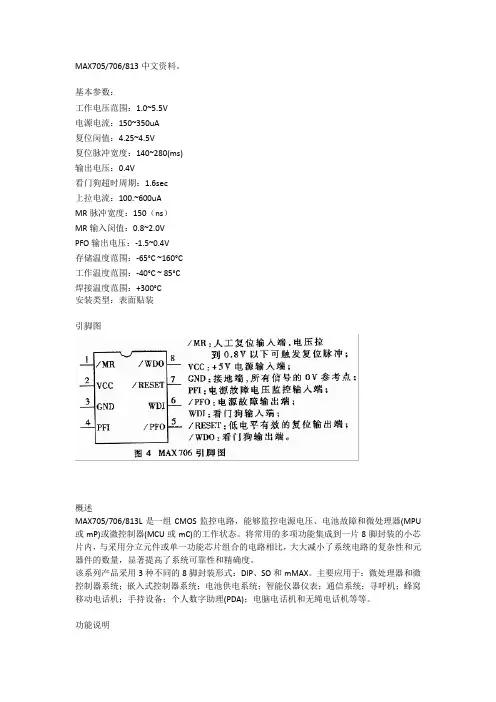
MAX705/706/813中文资料。
基本参数:工作电压范围:1.0~5.5V电源电流:150~350uA复位闵值:4.25~4.5V复位脉冲宽度:140~280(ms)输出电压:0.4V看门狗超时周期:1.6sec上拉电流:100.~600uAMR脉冲宽度:150(ns)MR输入闵值:0.8~2.0VPFO输出电压:-1.5~0.4V存储温度范围:-65°C ~160°C工作温度范围:-40°C ~ 85°C焊接温度范围:+300°C安装类型:表面贴装引脚图概述MAX705/706/813L是一组CMOS监控电路,能够监控电源电压、电池故障和微处理器(MPU 或mP)或微控制器(MCU或mC)的工作状态。
将常用的多项功能集成到一片8脚封装的小芯片内,与采用分立元件或单一功能芯片组合的电路相比,大大减小了系统电路的复杂性和元器件的数量,显著提高了系统可靠性和精确度。
该系列产品采用3种不同的8脚封装形式:DIP、SO和mMAX。
主要应用于:微处理器和微控制器系统;嵌入式控制器系统;电池供电系统;智能仪器仪表;通信系统;寻呼机;蜂窝移动电话机;手持设备;个人数字助理(PDA);电脑电话机和无绳电话机等等。
功能说明RESET/RESET操作复位信号用于启动或者重新启动MPU/MCU,令其进入或者返回到预知的循环程序并顺序执行。
一旦MPU/MCU处于未知状态,比如程序“跑飞”或进入死循环,就需要将系统复位。
对于MAX705和MAX706而言,在上电期间只要Vcc大于1.0V,就能保证输出电压不高于0.4V的低电平。
在Vcc上升期间RESET维持低电平直到电源电压升至复位门限(4.65V或4.40V)以上。
在超过此门限后,内部定时器大约再维持200ms后释放RESET,使其返回高电平。
无论何时只要电源电压降低到复位门限以下(即电源跌落),RESET引脚就会变低。

General DescriptionThe MAX3050/MAX3057 interface between the CAN protocol controller and the physical wires of the bus lines in a controller area network (CAN). They are pri-marily intended for automotive systems requiring data rates up to 2Mbps and feature ±80V fault protection against short circuits in high-voltage power buses. They provide differential transmit capability to the bus and differential receive capability to the CAN controller. The MAX3050/MAX3057 have four modes of operation:high speed, slope control, standby, and shutdown.High-speed mode allows data rates up to 2Mbps. In slope-control mode, data rates are 40kbps to 500kbps,so the effects of EMI are reduced, and unshielded twisted or parallel cable can be used. In standby mode,the transmitters are shut off and the receivers are put into low-current mode. In shutdown mode, the transmit-ter and receiver are switched off.The MAX3050 has an AutoShutdown™ function that puts the device into a 15µA shutdown mode when the bus or CAN controller is inactive for 4ms or longer.The MAX3050/MAX3057 are available in an 8-pin SO package and are specified for operation from -40°C to +125°C.ApplicationsAutomotive Systems HVAC Controls Telecom 72V systemsFeatureso ±80V Fault Protection for 42V Systems o Four Operating ModesHigh-Speed Operation Up to 2Mbps Slope-Control Mode to Reduce EMI (40kbps to 500kbps)Standby ModeLow-Current Shutdown Mode o AutoShutdown when Device Is Inactive (MAX3050)o Automatic Wake-Up from Shutdown (MAX3050)o Thermal Shutdown o Current Limitingo Fully Compatible with the ISO 11898 Standard*MAX3050/MAX3057±80V Fault-Protected, 2Mbps, Low SupplyCurrent CAN Transceivers________________________________________________________________Maxim Integrated Products 1Ordering InformationTypical Operating Circuit19-2670; Rev 0; 10/02For pricing, delivery, and ordering information,please contact Maxim/Dallas Direct!at1-888-629-4642, or visit Maxim’s website at .Pin ConfigurationAutoShutdown is a trademark of Maxim Integrated Products, Inc.*Pending completion of testing.M A X 3050/M A X 3057±80V Fault-Protected, 2Mbps, Low Supply Current CAN Transceivers 2_______________________________________________________________________________________ABSOLUTE MAXIMUM RATINGSDC ELECTRICAL CHARACTERISTICS(V CC = +5V ±10%, R L = 60Ω, RS = GND, T A = T MIN to T MAX . Typical values are at V CC = +5V and T A = +25°C.)Stresses beyond those listed under “Absolute Maximum Ratings” may cause permanent damage to the device. These are stress ratings only, and functional operation of the device at these or any other conditions beyond those indicated in the operational sections of the specifications is not implied. Exposure to absolute maximum rating conditions for extended periods may affect device reliability.V CC to GND ............................................................-0.3V to +6V TXD, RS, RXD, SHDN to GND....................-0.3V to (V CC + 0.3V)CANH, CANL to GND..............................................-80V to +80V RXD Shorted to GND.................................................Continuous Continuous Power Dissipation (T A = +70°C)8-Pin SO (derate 5.9mW/°C above +70°C) .................470mWOperating Temperature Range .........................-40°C to +125°C Junction Temperature......................................................+150°C Storage Temperature Range.............................-65°C to +150°C Lead Temperature (soldering, 10s) ................................+300°CMAX3050/MAX3057±80V Fault-Protected, 2Mbps, Low SupplyCurrent CAN Transceivers_______________________________________________________________________________________3DC ELECTRICAL CHARACTERISTICS (continued)M A X 3050/M A X 3057±80V Fault-Protected, 2Mbps, Low Supply Current CAN Transceivers 4_______________________________________________________________________________________Note 1:As defined by ISO, bus value is one of two complementary logical values: dominant or recessive. The dominant value repre-sents the logical 1 and the recessive represents the logical 0. During the simultaneous transmission of the dominant and recessive bits, the resulting bus value is dominant. For MAX3050 and MAX3057 values, see the truth table in the Transmitter and Receiver sections.TIMING CHARACTERISTICSMAX3050/MAX3057±80V Fault-Protected, 2Mbps, Low SupplyCurrent CAN Transceivers_______________________________________________________________________________________5Figure 1. AC Test CircuitFigure 2. Timing Diagram for Dynamic Characteristics Figure 3. Time to Wake Up (t WAKE ) (MAX3050)M A X 3050/M A X 3057±80V Fault-Protected, 2Mbps, Low Supply Current CAN Transceivers 6_______________________________________________________________________________________Typical Operating Characteristics(V CC = 5V, R L = 60Ω, C L = 100pF, T A = +25°C, unless otherwise specified.)MAX3057SLEW RATE vs. R RSR RS (k Ω)S L E W R A T E (V /µs )1621248648510152025010200M A X 50 t o c 02S L E E P T I M E (m s )3002001002040608010000400MAX3050AutoShutdown vs. C SHDNC SHDN (nF)SUPPLY CURRENT vs. DATA RATEDATA RATE (kbps)S U P P L Y C U R R E N T (m A )160012008004002729313335252000RECEIVER PROPAGATION DELAY vs. TEMPERATURE, R RS = GNDTEMPERATURE (°C)R E C E I V E R P R O P A G A T I O N D E L A Y (n s )905520-15253545556515-50125DRIVER PROPAGATION DELAY vs. TEMPERATURE, R RS = GNDTEMPERATURE (°C)D R I VE R P R O P A G A T I O N D E L A Y (n s )925926-72025303515-40125RECEIVER OUTPUT LOW vs. OUTPUT CURRENTOUTPUT CURRENT (mA)V O L T A G E R X D (m V )2015105400800120016000025RECEIVER OUTPUT HIGH vs. OUTPUT CURRENTOUTPUT CURRENT (mA)V O L T A G E (V C C - R X D ) (m V )201510560012001800300024000025DIFFERENTIAL VOLTAGE vs. DIFFERENTIAL LOAD R LDIFFERENTIAL LOAD R L (Ω)D I F FE R E N T I A L V O L T A G E (V )25020015010050123400300SUPPLY CURRENTvs. TEMPERATURE IN STANDBY MODEM A X 3050 t o c 09TEMPERATURE (°C)S U P P L Y C U R R E N T (µA )905520-157510012515017520050-50125MAX3050/MAX3057±80V Fault-Protected, 2Mbps, Low SupplyCurrent CAN TransceiversLOOPBACK PROPAGATION DELAY vs. R RSM A X 350 t o c 10R RS (k Ω)L O O P B A C K P R O P A G A T I O N D E L A Y (n s )1501005020040060080010001200140000200RECEIVER PROPAGATION DELAYMAX3050 toc1140ns/divRXD 2V/divCANH - CANLDRIVER PROPAGATION DELAYMAX3050 toc131µs/divTXD 5V/divR RS = 24k ΩR RS = 100k ΩR RS = 180k ΩDRIVER PROPAGATION DELAY40ns/divTXD 2V/div CANH - CANLTypical Operating Characteristics (continued)(V CC = 5V, R L = 60Ω, C L = 100pF, T A = +25°C, unless otherwise specified.)Pin DescriptionM A X 3050/M A X 3057Detailed DescriptionThe MAX3050/MAX3057 interface between the protocol controller and the physical wires of the bus lines in a CAN. They are primarily intended for automotive appli-cations requiring data rates up to 2Mbps and feature ±80V fault protection against shorts in high-voltage sys-tems. This fault protection allows the devices to with-stand up to ±80V with respect to ground with no damage to the device. The built-in fault tolerance allows the device to survive in industrial and automotive environments with no external protection devices. The devices provide differential transmit capability to the bus and differential receive capability to the CAN con-troller (Figure 4).The device has four modes of operation: high speed,slope control, standby, and shutdown. In high-speed mode, slew rates are not limited, making 2Mbps transmis-sion speeds possible. Slew rates are controlled in slope-control mode, minimizing EMI and allowing use of unshielded twisted or parallel cable. In standby mode,receivers are active and transmitters are in high imped-ance. In shutdown mode, transmitters and receivers are turned off.The transceivers are designed to operate from a single +5V supply and draw 56mA of supply current in domi-nant state and 3.6mA in recessive state. In standby mode, supply current is reduced to 125µA. In shutdown mode, supply current is 15µA.CANH and CANL are output short-circuit current limited and are protected against excessive power dissipation by thermal-shutdown circuitry that places the driver outputs into a high-impedance state.Fault ProtectionThe MAX3050/MAX3057 feature ±80V fault protection.This extended voltage range of CANH and CANL bus lines allows use in high-voltage systems and communi-cation with high-voltage buses. If data is transmitting at 2Mbps, the fault protection is reduced to ±70V.TransmitterThe transmitter converts a single-ended input (TXD)from the CAN controller to differential outputs for the bus lines (CANH, CANL). The truth table for the trans-mitter and receiver is given in Table 1.±80V Fault-Protected, 2Mbps, Low Supply Current CAN Transceivers 8_______________________________________________________________________________________Figure 4. Functional DiagramHigh SpeedConnect RS to ground to set the MAX3050/MAX3057 to high-speed mode. When operating in high-speed mode, the MAX3050/MAX3057 can achieve transmis-sion rates of up to 2Mbps. Line drivers are switched on and off as quickly as possible. However, in this mode,no measures are taken to limit the rise and fall slope of the data signal, allowing for potential EMI emissions. If using the MAX3050/MAX3057 in high-speed mode, use shielded twisted-pair cable to avoid EMI problems.Slope ControlConnect a resistor from RS to ground to select slope-control mode (Table 2). In slope-control mode, the gates of the line drivers are charged with a controlled current, proportional to the resistor connected to the RS pin. Transmission speed ranges from 40kbps to 500kbps. Controlling the rise and fall slope reduces EMI and allows the use of an unshielded twisted pair or a parallel pair of wires as bus lines. The transfer func-tion for selecting the resistor value is given by:R RS (k Ω) = 12000/speed (in kbps)See the Slew Rate vs. R RS graph in the Typical Operating Characteristics section.ReceiverThe receiver reads differential input from the bus lines (CANH, CANL) and transfers this data as a single-ended output (RXD) to the CAN controller. It consists of a comparator that senses the difference ∆V = (CANH -CANL) with respect to an internal threshold of 0.7V. If this difference is positive (i.e., ∆V > 0.7V), a logic low ispresent at the RXD pin. If negative (i.e., ∆V < 0.7V), a logic high is present.The receiver always echoes the transmitted data.The CANH and CANL common-mode range is -7V to +12V. RXD is logic high when CANH and CANL are shorted or terminated and undriven. If the differential receiver input voltage (CANH - CANL) is less than or equal to 0.5V, RXD is logic high. If (CANH - CANL) is greater than or equal to 0.9V, RXD is logic low.StandbyIf a logic high level is applied to RS, the MAX3050/MAX3057 enter a low-current standby mode. In this mode, the transmitter is switched off and the receiver is switched to a low-current state. If dominant bits are detected, RXD switches to a low level. The microcon-troller should react to this condition by switching the transceiver back to normal operation (through RS). Due to the reduced power mode, the receiver is slower in standby mode, and the first message may be lost at higher bit rates.Thermal ShutdownIf the junction temperature exceeds +160°C, the device is switched off. The hysteresis is approximately 20°C,disabling thermal shutdown once the temperature reaches +140°C.Shutdown (MAX3057)Drive SHDN low to enter shutdown mode. In shutdown mode, the device is switched off. The outputs are high impedance to ±80V. The MAX3057 features a pullup at SHDN . If shutdown is forced low and then left floating,the device switches back to normal operating mode.MAX3050/MAX3057±80V Fault-Protected, 2Mbps, Low SupplyCurrent CAN TransceiversTable 1. Transmitter and Receiver Truth Tablelogical 0 and the recessive represents the logical 1. During the simultaneous transmission of the dominant and recessive bits, the result-ing bus value is dominant.Table 2. Mode Selection Truth TableM A X 3050/M A X 3057AutoShutdown (MAX3050)To manage power consumption, AutoShutdown puts the device into shutdown mode after the device has been inactive for a period of time. The value of an external capacitor (C SHDN ) connected to SHDN deter-mines the threshold of inactivity time, after which the AutoShutdown triggers. F loating SHDN allows the MAX3050 to automatically change from active mode to shutdown.Use a 100nF capacitor as C SHDN for a typical thresh-old of 20ms. Change the capacitor value according to the following equation to change the threshold time period.V SHDN is the threshold of SHDN guaranteed to be less than 2V in the Electrical Characteristics table. Drive SHDN high to turn the MAX3050 on and disable AutoShutdown.When the MAX3050 is in shutdown mode, only the wake-up comparator is active, and normal bus commu-nication is ignored. The remote master of the CAN sys-tem wakes up the MAX3050 with a signal greater than 9V on CANH. Internal circuitry in the MAX3050 puts the device in normal operation by driving SHDN high. The MAX3057 does not have the AutoShutdown feature.Driver Output ProtectionThe MAX3050/MAX3057 have several features that pro-tect them from damage. Thermal shutdown switches off the device and puts CANH and CANL into high imped-ance if the junction temperature exceeds +160°C.Thermal protection is needed particularly when a bus line is short circuited. The hysteresis for the thermal shutdown is approximately 20°C.Additionally, a current-limiting circuit protects the trans-mitter output stage against short-circuits to positive and negative battery voltage. Although the power dissipa-tion increases during this fault condition, this featureprevents destruction of the transmitter output stage.±80V Fault-Protected, 2Mbps, Low Supply Current CAN Transceivers 10______________________________________________________________________________________Figure 5. FFT Dominant Bus at 2MbpsFigure 6. FFT Recessive Bus at 2MbpsFigure 7. FFT Dominant Bus at 500kbpsApplications InformationReduced EMI and ReflectionsIn slope-control mode, the CANH and CANL outputs are slew-rate limited, minimizing EMI and reducing reflections caused by improperly terminated cables. In general, a transmitter ’s rise time relates directly to the length of an unterminated stub, which can be driven with only minor waveform reflections. The following equation expresses this relationship conservatively:Length = t RISE / (15ns/ft)where t RISE is the transmitter ’s rise time.The MAX3050 and MAX3057 require no special layout considerations beyond common practices. Bypass V CC to GND with a 0.1µF ceramic capacitor mounted close to the IC with short lead lengths and wide trace widths.Chip InformationTRANSISTOR COUNT: 1214PROCESS: BiCMOSMAX3050/MAX3057±80V Fault-Protected, 2Mbps, Low SupplyCurrent CAN Transceivers______________________________________________________________________________________11Figure 8. FFT Recessive Bus at 500kbpsFigure 9. FFT Dominant Bus at 62.5kbpsFigure 10. FFT Recessive Bus at 62.5kbpsM A X 3050/M A X 3057±80V Fault-Protected, 2Mbps, Low Supply Current CAN Transceivers Maxim cannot assume responsibility for use of any circuitry other than circuitry entirely embodied in a Maxim product. No circuit patent licenses are implied. Maxim reserves the right to change the circuitry and specifications without notice at any time.12____________________Maxim Integrated Products, 120 San Gabriel Drive, Sunnyvale, CA 94086 408-737-7600©2002 Maxim Integrated ProductsPrinted USAis a registered trademark of Maxim Integrated Products.Package Information(The package drawing(s) in this data sheet may not reflect the most current specifications. For the latest package outline information,go to /packages .)。
_______________General DescriptionThe MAX306/MAX307 precision, monolithic, CMOS analog multiplexers (muxes) offer low on-resistance (less than 100Ω), which is matched to within 5Ωbetween channels and remains flat over the specified analog signal range (7Ωmax). They also offer low leak-age over temperature (I NO(OFF)less than 2.5nA at +85°C) and fast switching speeds (t TRANS less than 250ns). The MAX306 is a single-ended 1-of-16 device,and the MAX307 is a differential 2-of-8 device.The MAX306/MAX307 are fabricated with Maxim’s improved 44V silicon-gate process. Design improve-ments yield extremely low charge injection (less than 10pC) and guarantee electrostatic discharge (ESD)protection greater than 2000V.These muxes operate with a single +4.5V to +30V sup-ply, or bipolar ±4.5V to ±20V supplies, while retaining TTL/CMOS-logic input compatibility and fast switching.CMOS inputs provide reduced input loading. These improved parts are plug-in upgrades for the industry-standard DG406, DG407, DG506A, and DG507A.________________________ApplicationsSample-and-Hold Circuits Test Equipment Heads-Up DisplaysGuidance and Control Systems Military RadiosCommunications Systems Battery-Operated Systems PBX, PABXAudio Signal Routing____________________________Featureso Guaranteed On-Resistance Match Between Channels, <5ΩMaxo Low On-Resistance, <100ΩMaxo Guaranteed Flat On-Resistance over Specified Signal Range, 7ΩMaxo Guaranteed Charge Injection, <10pC o I NO(OFF)Leakage <2.5nA at +85°C o I COM(OFF)Leakage <20nA at +85°C o ESD Protection >2000Vo Plug-In Upgrade for Industry-Standard DG406/DG407/DG506A/DG507Ao Single-Supply Operation (+4.5V to +30V)Bipolar-Supply Operation (±4.5V to ±20V)o Low Power Consumption, <1.25mW o Rail-to-Rail Signal Handling o TTL/CMOS-Logic CompatibleMAX306/MAX307Precision, 16-Channel/Dual 8-Channel,High-Performance, CMOS Analog Multiplexers________________________________________________________________Maxim Integrated Products 1_____________________Pin Configurations/Functional Diagrams/Truth TablesCall toll free 1-800-998-8800 for free samples or literature.19-0270; Rev 0; 8/94Ordering Information continued at end of data sheet.* Contact factory for dice specifications.M A X 306/M A X 307Precision, 16-Channel/Dual 8-Channel,High-Performance, CMOS Analog Multiplexers 2_______________________________________________________________________________________ABSOLUTE MAXIMUM RATINGSELECTRICAL CHARACTERISTICS—Dual Supplies(V+ = +15V, V- = -15V, GND = 0V, V AH = +2.4V, V AL = +0.8V, T A = T MIN to T MAX , unless otherwise noted.)Stresses beyond those listed under “Absolute Maximum Ratings” may cause permanent damage to the device. These are stress ratings only, and functional operation of the device at these or any other conditions beyond those indicated in the operational sections of the specifications is not implied. Exposure to absolute maximum rating conditions for extended periods may affect device reliability.Voltage Referenced to V-V+............................................................................-0.3V, 44V GND.........................................................................-0.3V, 25V Digital Inputs, NO, COM (Note 1)...........(V- - 2V) to (V+ + 2V) or30mA (whichever occurs first)Continuous Current (any terminal)......................................30mA Peak Current, NO or COM(pulsed at 1ms, 10% duty cycle max)..........................100mA Continuous Power Dissipation (T A = +70°C)Plastic DIP (derate 9.09mW/°C above +70°C)............727mW Wide SO (derate 12.50mW/°C above +70°C)............1000mW PLCC (derate 10.53mW/°C above +70°C)..................842mW CERDIP (derate 16.67mW/°C above +70°C).............1333mW Operating Temperature RangesMAX30_C_ _.......................................................0°C to +70°C MAX30_E_ _.....................................................-40°C to +85°C MAX30_MJI....................................................-55°C to +125°C Storage Temperature Range.............................-65°C to +150°C Lead Temperature (soldering, 10sec).............................+300°CNote 1:Signals on NO, COM, A0, A1, A2, A3, or EN exceeding V+ or V- are clamped by internal diodes. Limit forward current to maximum current ratings.MAX306/MAX307Precision, 16-Channel/Dual 8-Channel,High-Performance, CMOS Analog Multiplexers_______________________________________________________________________________________3ELECTRICAL CHARACTERISTICS—Dual Supplies (continued)(V+ = +15V, V- = -15V, GND = 0V, V= +2.4V, V = +0.8V, T = T to T , unless otherwise noted.)M A X 306/M A X 307Precision, 16-Channel/Dual 8-Channel,High-Performance, CMOS Analog Multiplexers 4_______________________________________________________________________________________ELECTRICAL CHARACTERISTICS—Single Supply(V+ = +12V, V- = 0V, GND = 0V, V AH = +2.4V, V AL = +0.8V, T A = T MIN to T MAX , unless otherwise noted.)Note 2:The algebraic convention where the most negative value is a minimum and the most positive value a maximum is used inthis data sheet.Note 3:Guaranteed by design.Note 4:∆R ON = R ON(MAX)- R ON(MIN).On-resistance match between channels and flatness are guaranteed only with specifiedvoltages. Flatness is defined as the difference between the maximum and minimum value of on-resistance as measured at the extremes of the specified analog signal range.Note 5:Leakage parameters are 100% tested at the maximum rated hot temperature and guaranteed by correlation at +25°C.Note 6:Off isolation = 20log V COM /V NO , where V COM = output and V NO = input to off switch.MAX306/MAX307Precision, 16-Channel/Dual 8-Channel,High-Performance, CMOS Analog Multiplexers_______________________________________________________________________________________5120140160ON-RESISTANCE vs. V COM(DUAL SUPPLIES)1000204060-2020-1515-1010-5580V COM (V)R O N (Ω)120ON-RESISTANCE vs. V COM AND TEMPERATURE (DUAL SUPPLIES)1000204060-1515-1010-55080V COM (V)R O N (Ω)280320360400ON-RESISTANCE vs. V COM (SINGLE SUPPLY)24040801201601520105200V COM (V)R O N (Ω)120140160ON-RESISTANCE vs. V COM AND TEMPERATURE (SINGLE SUPPLY)10002040601510580V COM (V)R O N (Ω)30CHARGE INJECTION vs. V COM20-30-20-100-1515-1010-55010V COM (V)Q j (p C )100.0001-55125OFF LEAKAGE vs. TEMPERATURE1TEMPERATURE (°C)O F F L E A K A G E (n A )250.010.001-35-15650.1100100045851055100.0001-55125ON LEAKAGE vs. TEMPERATURE1TEMPERATURE (°C)O N L E A K A G E (n A )250.010.001-35-15650.11001000458510551000.001-55125SUPPLY CURRENT vs. TEMPERATURE10TEMPERATURE (°C)I +, I - (µA )250.10.01-35-1565145851055__________________________________________Typical Operating Characteristics(T A = +25°C, unless otherwise noted.)__________Applications InformationOperation with Supply VoltagesOther than ±15VUsing supply voltages other than ±15V will reduce the analog signal range. The MAX306/MAX307 switches operate with ±4.5V to ±20V bipolar supplies or with a +4.5V to +30V single supply; connect V- to GND when operating with a single supply. Also, both device types can operate with unbalanced supplies such as +24V and -5V. The Typical Operating Characteristics graphs show typical on-resistance with 20V, 15V, 10V, and 5V supplies. (Switching times increase by a factor of two or more for operation at 5V.)Overvoltage ProtectionProper power-supply sequencing is recommended for all CMOS devices. Do not exceed the absolute maxi-mum ratings because stresses beyond the listed rat-ings may cause permanent damage to the devices.Always sequence V+ on first, then V-, followed by either the logic inputs, NO, or COM. If power-supply sequencing is not possible, add two small signal diodes in series with supply pins for overvoltage pro-tection (Figure 1). Adding diodes reduces the analogsignal range to 1V above V+ and 1V below V-, but low switch resistance and low leakage characteristics are unaffected. Device operation is unchanged, and the difference between V+ and V- should not exceed +44V.M A X 306/M A X 307Precision, 16-Channel/Dual 8-Channel,High-Performance, CMOS Analog Multiplexers 6_______________________________________________________________________________________Output–bidirectionalCOM28Address Inputs A3–A014–17Enable InputsEN 18Analog Inputs–bidirectional NO1–NO819–26Negative Supply Voltage Input V-27Ground GND 12Analog Inputs–bidirectional NO16–NO94–11MAX306PINNo Internal Connections N.C.2, 3, 13Positive Supply Voltage Input V+1FUNCTIONNAME_____________________________________________________________Pin DescriptionsDiodesMAX306/MAX307Precision, 16-Channel/Dual 8-Channel,High-Performance, CMOS Analog Multiplexers_______________________________________________________________________________________7______________________________________________Test Circuits/Timing DiagramsM A X 306/M A X 307Precision, 16-Channel/Dual 8-Channel,High-Performance, CMOS Analog Multiplexers 8________________________________________________________________________________________________________________________Test Circuits/Timing Diagrams (continued)Figure 5. Charge InjectionMAX306/MAX307Precision, 16-Channel/Dual 8-Channel,High-Performance, CMOS Analog Multiplexers_______________________________________________________________________________________9_________________________________Test Circuits/Timing Diagrams (continued)Figure 8. NO/COM CapacitanceM A X 306/M A X 307Precision, 16-Channel/Dual 8-Channel,High-Performance, CMOS Analog Multiplexers 10______________________________________________________________________________________________Pin Configurations/Functional Diagrams/Truth Tables (continued)A2A1A0EN ON Switch X 0 0 0 0 1 1 1 1 0 0 0 0 1 1 1 1X 0 0 1 1 0 0 1 1 0 0 1 1 0 0 1 1X 0 1 0 1 0 1 0 1 0 1 0 1 0 1 0 10 1 1 1 1 1 1 1 1 1 1 1 1 1 1 1 1None 1 2 3 4 5 6 7 8 9 10 11 12 13 14 15 16MAX306LOGIC “0” V AL ≤ 0.8V, LOGIC “1” = V AH ≥ 2.4VA3X 0 0 0 0 0 0 0 0 1 1 1 1 1 1 11A2A1A0EN ON Switch X 0 0 0 0 1 1 1 1X 0 0 1 1 0 0 1 1X 0 1 0 1 0 1 0 10 1 1 1 1 1 1 1 1None 1 2 3 4 5 6 7 8MAX307LOGIC “0” V AL ≤ 0.8V, LOGIC “1” = V AH ≥ 2.4VMAX306/MAX307Precision, 16-Channel/Dual 8-Channel,High-Performance, CMOS Analog Multiplexers______________________________________________________________________________________11________Pin Configurations/Functional Diagrams/Truth Tables (continued)_Ordering Information (continued)* Contact factory for dice specifications.Maxim cannot assume responsibility for use of any circuitry other than circuitry entirely embodied in a Maxim product. No circuit patent licenses are implied. Maxim reserves the right to change the circuitry and specifications without notice at any time.12__________________Maxim Integrated Products, 120 San Gabriel Drive, Sunnyvale, CA 94086 (408) 737-7600©1994 Maxim Integrated ProductsPrinted USAis a registered trademark of Maxim Integrated Products.M A X 306/M A X 307Precision, 16-Channel/Dual 8-Channel,High-Performance, CMOS Analog Multiplexers __________________________________________________________Chip TopographiesGNDNO1 NO2 NO3 N04 NO5 NO6 NO7 NO80.184" (4.67mm)0.078" (1.98mm)NO9NO10NO11NO12N013NO14NO15NO16N.C.V-COM V+GND NO1A NO2A NO3A N04A NO5A NO6A NO7A NO8A0.184" (4.67mm)0.078" (1.98mm)NO1B NO2B NO3B NO4B N05B NO6B NO7B NO8B COMBV-COMA V+TRANSISTOR COUNT: 269SUBSTRATE IS INTERNALLY CONNECTED TO V+TRANSISTOR COUNT: 269SUBSTRATE IS INTERNALLY CONNECTED TO V+MAX306MAX307N.C. = NO INTERNAL CONNECTION。