TM202
- 格式:pdf
- 大小:263.13 KB
- 文档页数:3
纳米增韧剂FoRTEGRArM202增韧环氧胶粘剂的研究作者:冯艳丽彭秋柏杜伟等来源:《粘接》2014年第10期摘要:阐述了环氧树脂的增韧方法和机理,对陶氏化学FORTEGRATM 202环氧增韧剂在不同固化体系中的性能表现进行了研究。
并与环氧胶粘剂中常用的端羧基丁腈橡胶(CTBN)或与环氧预聚的端羧基丁腈橡胶CTBN-Epoxy进行了性能对比。
研究表明FORTEGRATM 202环氧增韧剂除产品本身的低黏度所带来的配方调整空间更大的优势外,固化物还具有玻璃化转变温度高,拉剪强度更高,断裂韧性和透明度更好等优势。
关键词:环氧树脂;增韧剂;端羧基丁腈橡胶(CTBN);环氧预聚的端羧基丁腈橡胶(CTBN-Epoxy)环氧树脂具有良好的介电性能、化学稳定性、粘接性和加工性等特性,在航空、航天、汽车、电子电气等领域发挥重要的作用。
但是环氧树脂固化后交联密度很高,其裂纹扩展属于典型的脆性扩展,固化后韧性不足、耐冲击性较差、容易开裂,使其在一些对韧性要求较高的领域的应用受到一定限制。
因此如何提高固化后环氧树脂的韧性一直是学术界和工业界研究的热门课题[1~6]。
环氧胶粘剂做为环氧树脂的一个重要应用,韧性是其必不可少的一个重要性能指标,因此选择合适的增韧剂对提高环氧胶粘剂的综合性能至关重要。
本文选取了环氧胶粘剂中常用的增韧剂,包括端羧基丁腈橡胶(CTBN)和环氧预聚的端羧基丁腈橡胶(CTBN-Epoxy),与陶氏化学新开发的新型纳米增韧剂FORTEGRATM 202进行对比研究,考查了它们在各种环氧树脂胶粘剂体系中的性能,发现在固化过程中FORTEGRATM 202形成了更为细小、达到纳米尺度并均匀分布的相区,相应的环氧树脂固化物在耐热性、断裂韧性、拉剪强度方面等有更大的提高。
1 实验部分1.1 主要原料D.E.R.TM 331,液态双酚A环氧树脂,陶氏化学;甲基四氢苯酐(MTHPA),工业级,玻琳化学;聚酰胺D.E.H.TM 140,工业级,陶氏化学;双氰胺(DICY),工业级,赢创;端羧基丁腈橡胶环氧增韧剂Hycar CTBN 1300X8,工业级,CVC Thermoset Specialties;环氧预聚端羧基丁腈橡胶环氧增韧剂FORTEGRATM 201,CTBN含量40%,陶氏化学;环氧增韧剂FORTEGRATM 202、多乙烯多胺TETA,陶氏化学。
TM=2a q201杭州i=9634.9(1+0.927LgP)/(t+31.546)1.008 (L/s•ha)2322临安i=1307.9(1+0.784LgP)/(t+6.124)0.623 (L/s•ha)2123富阳i=3254.3(1+0.682LgP)/(t+19.584)0.791 (L/s•ha)2144桐庐i=6113.9(1+0.688LgP)/(t+28.149)0.940 (L/s•ha)1945建德i=2746.7(1+0.803LgP)/(t+13.427)0.806 (L/s•ha)2026淳安i=1863.0(1+0.796LgP)/(t+11.470)0.734 (L/s•ha)1847宁波i=16566.6(1+0.856LgP)/(t+32.196)1.113(L/s•ha)2568余姚i=2559.8(1+0.783LgP)/(t+13.474)0.751 (L/s•ha)2279慈溪i=5490.6(1+0.731LgP)/(t+29.767)0.860 (L/s•ha)23310鄞州i=1167.6(1+1.097LgP)/(t+6.536)0.613(L/s•ha)20911奉化i=11320.9(1+0.759LgP)/(t+29.294)1.041 (L/s•ha)24112镇海i=10705.5(1+0.803LgP)/(t+32.135)1.007 (L/s•ha)24813宁海i=2757.0(1+0.645LgP)/(t+15.435)0.710 (L/s•ha)26214象山i=1611.8(1+1.038LgP)/(t+9.823)0.655 (L/s•ha)22915温州i=757.7(1+0.711LgP)/(t+3.528)0.422 (L/s•ha)24316瑞安i=2363.5(1+0.698LgP)/(t+16.298)0.716 (L/s•ha)21917乐清i=1195.4(1+0.675LgP)/(t+10.724)0.538 (L/s•ha)22818永嘉i=1907.0(1+0.687LgP)/(t+14.497)0.616 (L/s•ha)26019平阳i=1147.4(1+0.776LgP)/(t+8.056)0.542 (L/s•ha)23320苍南i=1107.7(1+0.595LgP)/(t+9.571)0.506 (L/s•ha)236城市名称暴雨强度公式浙江省各城市暴雨强度公式成果表温州市序号所在地区杭州市宁波市21文成i=3035.1(1+0.622LgP)/(t+15.237)0.733 (L/s•ha)26522泰顺i=1575.5(1+0.709LgP)/(t+12.648)0.599 (L/s•ha)23723嘉兴i=1773.8(1+0.675LgP)/(t+10.647)0.655 (L/s•ha)22724海宁i=1683.8(1+1.057LgP)/(t+11.300)0.682 (L/s•ha)21225平湖i=1919.4(1+0.896LgP)/(t+11.574)0.695 (L/s•ha)22226桐乡i=4454.1(1+0.902LgP)/(t+22.984)0.876 (L/s•ha)21027海盐i=4164.0(1+1.287LgP)/(t+18.321)0.900 (L/s•ha)21728嘉善i=5778.3(1+0.848LgP)/(t+28.102)0.877 (L/s•ha)243湖州i=3849.1(1+0.989LgP)/(t+18.862)0.842 (L/s•ha)23030长兴i=1568.5(1+0.951LgP)/(t+9.566)0.643 (L/s•ha)22931安吉i=1940.9(1+0.656LgP)/(t+13.122)0.683 (L/s•ha)21332德清i=838.5(1+0.858LgP)/(t+4.298)0.485 (L/s•ha)22533绍兴i=2939.8(1+0.764LgP)/(t+12.882)0.811(L/s•ha)21334诸暨i=2146.1(1+1.001LgP)/(t+9.867)0.761 (L/s•ha)21135上虞i=6058.7(1+0.658LgP)/(t+17.861)0.945 (L/s•ha)23536嵊州i=8092.3(1+0.822LgP)/(t+22.695)1.026 (L/s•ha)21537新昌i=6524.6(1+0.751LgP)/(t+28.589)0.920 (L/s•ha)22538金华i=1108.6(1+0.947LgP)/(t+3.573)0.616 (L/s•ha)20439兰溪i=7945.6(1+0.787LgP)/(t+23.285)1.038 (L/s•ha)19740东阳i=2121.9(1+0.906LgP)/(t+12.574)0.745 (L/s•ha)20241义乌i=1313.9(1+0.835LgP)/(t+5.129)0.662 (L/s•ha)19542永康i=1124.4(1+0.701LgP)/(t+6.725)0.585 (L/s•ha)20043武义i=1961.9(1+0.674LgP)/(t+11.175)0.728 (L/s•ha)193湖州市绍兴市金华市嘉兴市44磐安i=3051.6(1+0.798LgP)/(t+18.104)0.782 (L/s•ha)22045浦江i=8468.0(1+0.764LgP)/(t+25.736)1.027 (L/s•ha)20646衢州i=2712.5(1+0.730LgP)/(t+14.823)0.792 (L/s•ha)19947江山i=1454.6(1+0.600LgP)/(t+7.605)0.625 (L/s•ha)21648常山i=3687.2(1+0.611LgP)/(t+16.291)0.844 (L/s•ha)21149开化i=1599.0(1+0.575LgP)/(t+8.387)0.667 (L/s•ha)20250龙游i=4338.5(1+0.859LgP)/(t+18.131)0.904 (L/s•ha)20351舟山i=765.0(1+0.856LgP)/(t+6.650)0.516(L/s•ha)17752定海i=3893.9(1+0.775LgP)/(t+20.151)0.848 (L/s•ha)21053台州i=1654.5(1+0.618LgP)/(t+11.952)0.631 (L/s•ha)22154临海i=28827.8(1+0.655LgP)/(t+49.157)1.165 (L/s•ha)24955温岭i=24822.6(1+0.860LgP)/(t+55.187)1.119 (L/s•ha)24956仙居i=2329.8(1+0.679LgP)/(t+16.142)0.715(L/s•ha)21657天台i=2005.7(1+0.727LgP)/(t+11.781)0.712 (L/s•ha)20958黄岩i=1525.8(1+0.631LgP)/(t+11.208)0.571 (L/s•ha)25559三门i=1727.7(1+0.680LgP)/(t+10.569)0.638 (L/s•ha)23560玉环i=924.0(1+0.862LgP)/(t+5.116)0.509 (L/s•ha)22661丽水i=1265.3(1+0.587LgP)/(t+5.919)0.611 (L/s•ha)20462龙泉i=15672.8(1+0.636LgP)/(t+32.885)1.139 (L/s•ha)20463青田i=1817.0(1+0.662LgP)/(t+8.983)0.676 (L/s•ha)22464庆元i=1081.0(1+0.477LgP)/(t+5.728)0.579 (L/s•ha)18965缙云i=1157.6(1+0.683LgP)/(t+4.400)0.606 (L/s•ha)20266遂昌i=1667.2(1+0.600LgP)/(t+8.592)0.690 (L/s•ha)195舟山市台州市丽水市衢州市67松阳i=9151.2(1+0.651LgP)/(t+28.102)1.023 (L/s•ha)205 68云和i=1460.8(1+0.815LgP)/(t+8.551)0.657 (L/s•ha)201 69景宁i=2130.3(1+0.816LgP)/(t+14.445)0.719 (L/s•ha)209。
202材质含量标准
"202材质"一般指的是不锈钢材质,其中包括了 SUS202(日本材料牌号)和 1Cr18Mn8Ni5N(中国材料牌号)等。
不锈钢材质的含量标准有以下几项:
1. 碳含量(C):一般要求小于0.15%。
2. 硅含量(Si):一般要求小于1%。
3. 锰含量(Mn):一般要求小于7%。
4. 磷含量(P):一般要求小于0.045%。
5. 硫含量(S):一般要求小于0.03%。
6. 铬含量(Cr):一般要求在16%-18%之间。
7. 镍含量(Ni):一般要求在4%-6%之间。
8. 氮含量(N):一般要求小于0.25%。
需要注意的是,以上含量标准仅供参考,实际标准可能会根据不同的制造标准和要求而有所调整。
使用时还需根据具体材料牌号和产品标准进行确认。
TM 电工技术TM 电工技术机电一体化入TH-39。
[TM-9] 电工技术经济易入F407.6。
TM0 一般性问题TM02 电工设计、制图TM05 电工安装技术TM07 电工保养、维修TM08 电工安全TM1 电工基础理论电力电子学入此。
TM11 电工单位、电工计算[TM12] 电学、磁学宜入O441。
TM13 电路理论TM131 线性电路{TM131.1} 电路拓扑学停用;4版改入TM13。
TM131.2 过渡过程、暂态过程TM131.3 直流电路TM131.4 交流电路TM131.4+1 谐振电路、耦合电路TM131.4+2 圆图及反演TM131.4+3 多相电路TM131.4+4 对称分量TM131.4+6 多端网络[TM131.5] 逻辑电路TM131.6 时变电路TM132 非线性电路、铁心电路TM133 电路综合与分析TM134 分布参数电路TM135 电路参数TM14 磁路TM141 磁导TM142 直流磁路TM143 交流磁路TM144 永久磁铁磁路TM15 电磁场理论的应用TM151 静电场计算方法TM151+.1 二度场计算TM151+.2 三度场计算TM151+.3 电容及部分电容TM152 电流场、电流场计算TM153 磁场、磁场计算TM153+.1 磁场计算TM153+.2 电感计算TM153+.3 电磁力[TM153+.4] 地磁TM153+.5 磁屏蔽TM154 交变电磁场TM154.1 交变电磁场计算TM154.2 导电体中电磁过程及其应用。
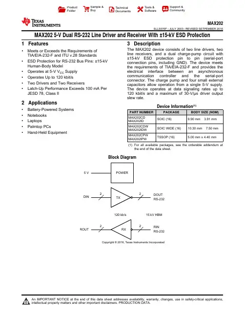
5 V DINROUTDOUT RS-232RIN RS-232120 kb/s15 kV HBMCopyright © 2016,Texas Instruments IncorporatedProduct FolderSample &BuyTechnical Documents Tools &SoftwareSupport &CommunityAn IMPORTANT NOTICE at the end of this data sheet addresses availability,warranty,changes,use in safety-critical applications,intellectual property matters and other important disclaimers.PRODUCTION DATA.MAX202SLLS576F –JULY 2003–REVISED SETPEMBER 2016MAX2025-V Dual RS-232Line Driver and Receiver With ±15-kV ESD Protection1Features•Meets or Exceeds the Requirements of TIA/EIA-232-F and ITU v.28Standards•ESD Protection for RS-232Bus Pins:±15-kV Human-Body Model•Operates at 5-V V CC Supply •Operates Up to 120kbit/s•Two Drivers and Two Receivers•Latch-Up Performance Exceeds 100mA Per JESD 78,Class II2Applications•Battery-Powered Systems •Notebooks •Laptops•Palmtop PCs•Hand-Held Equipment3DescriptionThe MAX202device consists of two line drivers,two line receivers,and a dual charge-pump circuit with ±15-kV ESD protection pin to pin (serial-port connection pins,including GND).The device meets the requirements of TIA/EIA-232-F and provides the electrical interface between an asynchronous communication controller and the serial-port connector.The charge pump and four small external capacitors allow operation from a single 5-V supply.The device operates at data signaling rates up to 120kbit/s and a maximum of 30-V/µs driver output slew rate.Device Information (1)PART NUMBER PACKAGE BODY SIZE (NOM)MAX202CD MAX202ID SOIC (16)9.90mm ×3.91mm MAX202CDW MAX202IDW SOIC WIDE (16)10.30mm ×7.50mm MAX202CPW MAX202IPWTSSOP (16)5.00mm x 4.40mm(1)For all available packages,see the orderable addendum atthe end of the data sheet.Block Diagram2MAX202SLLS576F –JULY 2003–REVISED SETPEMBER 2016Product Folder Links:MAX202Submit Documentation FeedbackCopyright ©2003–2016,Texas Instruments IncorporatedTable of Contents1Features ..................................................................12Applications ...........................................................13Description .............................................................14Revision History .....................................................25Pin Configuration and Functions . (36)Specifications .........................................................46.1Absolute Maximum Ratings......................................46.2ESD Ratings..............................................................46.3Recommended Operating Conditions.......................46.4Thermal Information..................................................46.5Electrical Characteristics...........................................56.6Switching Characteristics..........................................56.7Typical Characteristics .............................................67Parameter Measurement Information ..................78Detailed Description . (8)8.1Overview...................................................................88.2Functional Block Diagram.. (8)8.3Feature Description...................................................88.4Device Functional Modes (8)9Application and Implementation (10)9.1Application Information............................................109.2Typical Application.. (10)10Power Supply Recommendations .....................1311Layout . (13)11.1Layout Guidelines ................................................1311.2Layout Example. (13)12Device and Documentation Support (14)12.1Receiving Notification of Documentation Updates 1412.2Community Resources..........................................1412.3Trademarks...........................................................1412.4Electrostatic Discharge Caution............................1412.5Glossary................................................................1413Mechanical,Packaging,and OrderableInformation (14)4Revision HistoryNOTE:Page numbers for previous revisions may differ from page numbers in the current version.Changes from Revision E (April 2007)to Revision F Page•Added ESD Ratings table,Feature Description section,Device Functional Modes ,Application and Implementation section,Power Supply Recommendations section,Layout section,Device and Documentation Support section,andMechanical,Packaging,and Orderable Information section..................................................................................................1•Removed the Ordering Information table;see POA at the end of the data sheet .................................................................1•Changed values in the Thermal Information table to align with JEDEC standards (4)C1+ V CC V+ GND C1± DOUT1C2+ RIN1C2± ROUT1V ± DIN1DOUT2 DIN2RIN2ROUT23MAX202SLLS576F –JULY 2003–REVISED SETPEMBER 2016Product Folder Links:MAX202Submit Documentation FeedbackCopyright ©2003–2016,Texas Instruments Incorporated 5Pin Configuration and FunctionsD,DW,or PW Package 16-Pin SOIC or TSSOPTop ViewPin FunctionsPINI/O DESCRIPTION 1C1+—Positive lead of C1capacitor2V+O Positive charge pump output for storage capacitor only 3C1–—Negative lead of C1capacitor 4C2+—Positive lead of C2capacitor 5C2–—Negative lead of C2capacitor6V–O Negative charge pump output for storage capacitor only 7DOUT2O RS-232line data output (to remote RS-232system)8RIN2I RS-232line data input (from remote RS-232system)9ROUT2O Logic data output (to UART)10DIN2I Logic data input (from UART)11DIN1I Logic data input (from UART)12ROUT1O Logic data output (to UART)13RIN1I RS-232line data input (from remote RS-232system)14DOUT1O RS-232line data output (to remote RS-232system)15GND —Ground16V CC—Supply voltage,connect to external 5-V power supply4MAX202SLLS576F –JULY 2003–REVISED SETPEMBER 2016Product Folder Links:MAX202Submit Documentation FeedbackCopyright ©2003–2016,Texas Instruments Incorporated(1)Stresses beyond those listed under Absolute Maximum Ratings may cause permanent damage to the device.These are stress ratings only,which do not imply functional operation of the device at these or any other conditions beyond those indicated under Recommended Operating Conditions .Exposure to absolute-maximum-rated conditions for extended periods may affect device reliability.(2)All voltages are with respect to network GND.6Specifications6.1Absolute Maximum Ratingsover operating free-air temperature range (unless otherwise noted)(1)MINMAX UNIT Supply voltage,V CC (2)–0.36V Positive charge pump voltage,V+(2)V CC –0.314V Negative charge pump voltage,V–(2)–140.3V Input voltage,V I Drivers –0.3V++0.3V Receivers ±30Output voltage,V ODrivers V––0.3V++0.3VReceivers–0.3V CC +0.3Short-circuit duration,D OUTContinuousOperating junction temperature,T J 150°C Storage temperature,T stg –65150°C (1)JEDEC document JEP155states that 500-V HBM allows safe manufacturing with a standard ESD control process.(2)JEDEC document JEP157states that 250-V CDM allows safe manufacturing with a standard ESD control process.6.2ESD RatingsVALUEUNITV (ESD)Electrostatic dischargeHuman-body model (HBM),per ANSI/ESDA/JEDEC JS-001(1)Pins 7,8,13,and 14±15000V All other pins±2000Charged-device model (CDM),per JEDEC specification JESD22-C101(2)±1500(1)Test conditions are C1–C4=0.1µF at V CC =5V ±0.5V.6.3Recommended Operating Conditionsover operating free-air temperature range (unless otherwise noted (1);see Figure 10)MINNOMMAX UNIT Supply voltage4.555.5V V IH Driver high-level input voltage (D IN )2V V IL Driver low-level input voltage (D IN )0.8V V I Driver input voltage (D IN )0 5.5V Receiver input voltage –3030T A Operating free-air temperatureMAX202C 070°CMAX202I–4085(1)For more information about traditional and new thermal metrics,see the Semiconductor and IC Package Thermal Metrics application report.6.4Thermal InformationTHERMAL METRIC (1)MAX202UNITD (SOIC)DW (SOIC)PW (TSSOP)16PINS 16PINS 16PINS R θJA Junction-to-ambient thermal resistance 76.276.8101°C/W R θJC(top)Junction-to-case (top)thermal resistance 36.839.636.4°C/W R θJB Junction-to-board thermal resistance 33.941.545.9°C/W ψJT Junction-to-top characterization parameter 6.712.6 2.7°C/W ψJB Junction-to-board characterization parameter33.640.945.3°C/W5MAX202SLLS576F –JULY 2003–REVISED SETPEMBER 2016Product Folder Links:MAX202Submit Documentation FeedbackCopyright ©2003–2016,Texas Instruments Incorporated (1)Test conditions are C1–C4=0.1µF at V CC =5V ±0.5V.(2)All typical values are at V CC =5V,and T A =25°C.(3)Short-circuit durations should be controlled to prevent exceeding the device absolute power-dissipation ratings,and not more than one output should be shorted at a time.6.5Electrical Characteristicsover recommended ranges of supply voltage and operating free-air temperature (unless otherwise noted;see Figure 10)(1)PARAMETERTEST CONDITIONSMINTYP (2)MAX UNIT I CC Supply currentNo load,V CC =5V815mADRIVER SECTIONV OH High-level output voltage D OUT at R L =3k Ωto GND,D IN =GND 59V V OL Low-level output voltage D OUT at R L =3k Ωto GND,D IN =V CC –5–9V I IH High-level input current V I =V CC 0200µA I IL Low-level input current V I at 0V0–200µA I OS (3)Short-circuit output current V CC =5.5V,V O =0V±10±60mA r O Output resistance V CC ,V+,and V–=0V,V O =±2V 300ΩRECEIVER SECTIONV OH High-level output voltage I OH =–1mA 3.5V CC –0.4V V OL Low-level output voltageI OL =1.6mA 0.4V V IT+Positive-going input threshold voltage V CC =5V,T A =25°C 1.7 2.4V V IT–Negative-going input threshold voltage V CC =5V,T A =25°C0.8 1.2V V hys Input hysteresis (V IT+–V IT–)0.20.51V r i Input resistanceV I =±3V to ±25V357k Ω(1)Test conditions are C1–C4=0.1µF at V CC =5V ±0.5V.(2)All typical values are at V CC =5V,and T A =25°C.(3)Pulse skew is defined as |t PLH –t PHL |of each channel of the same device.6.6Switching Characteristicsover recommended ranges of suply voltage and operating free-air temperature (unless otherwise noted;see Figure 10)(1)PARAMETERTEST CONDITIONSMINTYP (2)MAXUNITDRIVER SECTIONMaximum data rateC L =50pF to 1000pF,R L =3k Ωto 7k ΩoneD OUT switching,see Figure 6120kbit/s t PLH(D)Propagation delay time,low-to high-level output C L =2500pF,R L =3k Ω,all drivers loaded,see Figure 62µs t PHL(D)Propagation delay time,high-to low-level output C L =2500pF,R L =3k Ω,all drivers loaded,see Figure 62µs t sk(p)Pulse skew (3)C L =150to 2500pF,R L =3k Ωto 7k Ω,see Figure 7300ns SR(tr)Slew rate,transition regionC L =50to 1000pF,R L =3k Ωto 7k Ω,V CC =5V,see Figure 63630V/µsRECEIVER SECTION (SEE Figure 8)t PLH(R)Propagation delay time,low-to high-level output C L =150pF 0.510µs t PHL(R)Propagation delay time,high-to low-level output C L =150pF 0.510µs t sk(p)Pulse skew (3)C L =150pF300ns6MAX202SLLS576F –JULY 2003–REVISED SETPEMBER 2016Product Folder Links:MAX202Submit Documentation FeedbackCopyright ©2003–2016,Texas Instruments Incorporated6.7Typical Characteristicsat T A =25°C (unless otherwise noted)TEST CIRCUITVOLTAGE WAVEFORMS50%50%–3 V3 V1.5 V1.5 VOutputInputV OL V OHt PHL (R)t PLH (R)OutputA)TEST CIRCUITVOLTAGE WAVEFORMS0 V 3 VOutputInputV OLV OHt PLH (D)t PHL (D)50%50%1.5 V1.5 VRS-232OutputA)TEST CIRCUITVOLTAGE WAVEFORMS0 V3 VOutputInputV OLV OH t PLH (D)RS-232Outputt PHL (D)A)1.5 V1.5 V3 V –3 V3 V –3 VSR(tf) =6 Vt or t PHL(D PLH(D))7MAX202SLLS576F –JULY 2003–REVISED SETPEMBER 2016Product Folder Links:MAX202Submit Documentation FeedbackCopyright ©2003–2016,Texas Instruments Incorporated 7Parameter Measurement InformationA.C L includes probe and jig capacitance.B.The pulse generator has the following characteristics:PRR =120kbit/s,Z O =50Ω,50%duty cycle,t r ≤10ns,t f ≤10ns.Figure 6.Driver Slew RateA.C L includes probe and jig capacitance.B.The pulse generator has the following characteristics:PRR =120kbit/s,Z O =50Ω,50%duty cycle,t r ≤10ns,t f ≤10ns.Figure 7.Driver Pulse SkewA.C L includes probe and jig capacitance.B.The pulse generator has the following characteristics:Z O =50Ω,50%duty cycle,t r ≤10ns,t f ≤10ns.Figure 8.Receiver Propagation Delay Times5 V DINROUTDOUT RS-232RIN RS-232120 kb/s15 kV HBMCopyright © 2016,Texas Instruments Incorporated8MAX202SLLS576F –JULY 2003–REVISED SETPEMBER 2016Product Folder Links:MAX202Submit Documentation FeedbackCopyright ©2003–2016,Texas Instruments Incorporated8Detailed Description8.1OverviewThe MAX202device is a dual driver and receiver that includes a capacitive voltage generator using four capacitors to supply TIA/EIA-232-F voltage levels from a single 5-V supply.Each receiver converts TIA/EIA-232-F inputs to 5-V TTL/CMOS levels.These receivers have shorted and open fail safe.The receiver can accept up to ±30-V inputs and decode inputs as low as ±3V.Each driver converts TTL/CMOS input levels into TIA/EIA-232-F levels.Outputs are protected against shorts to ground.8.2Functional Block Diagram8.3Feature Description8.3.1PowerThe power block increases and inverts the 5-V supply for the RS-232driver using a charge pump that requires four 0.1-µF external capacitors.8.3.2RS-232DriverTwo drivers interface standard logic levels to RS-232levels.The driver inputs do not have internal pullup resistors.Do not float the driver inputs.8.3.3RS-232ReceiverTwo Schmitt trigger receivers interface RS-232levels to standard logic levels.Each receiver has an internal 5-k Ωload to ground.An open input results in a high output on ROUT.8.4Device Functional Modes8.4.1V CC Powered by 5-VThe device is in normal operation when powered by 5V.8.4.2V CC UnpoweredWhen MAX202is unpowered,it can be safely connected to an active remote RS-232device.DIN1DOUT1RIN1ROUT1DIN2DOUT2RIN2ROUT29MAX202SLLS576F –JULY 2003–REVISED SETPEMBER 2016Product Folder Links:MAX202Submit Documentation FeedbackCopyright ©2003–2016,Texas Instruments Incorporated Device Functional Modes (continued)8.4.3Truth TablesTable 1and Table 2list the function for each driver and receiver (respectively).(1)H =high level,L =low levelTable 1.Function Table forEach Driver (1)INPUT DIN OUTPUT DOUTL H HL(1)H =high level,L =low level,Open =input disconnected or connected driver offTable 2.Function Table forEach Receiver (1)INPUT RIN OUTPUT ROUTL H H L OpenHFigure 9.Logic Diagram (Positive Logic)CBYPASS = 0.1F,m C10.1F,m 6.3 VCopyright © 2016,Texas Instruments Incorporated10MAX202SLLS576F –JULY 2003–REVISED SETPEMBER 2016Product Folder Links:MAX202Submit Documentation FeedbackCopyright ©2003–2016,Texas Instruments Incorporated9Application and ImplementationNOTEInformation in the following applications sections is not part of the TI component specification,and TI does not warrant its accuracy or completeness.TI’s customers are responsible for determining suitability of components for their purposes.Customers should validate and test their design implementation to confirm system functionality.9.1Application InformationFor proper operation,add capacitors as shown in Figure 10.Pins 9through 12connect to UART or general purpose logic lines.RS-232lines on pins 7,8,13,and 14connect to a connector or cable.9.2Typical ApplicationA.C3can be connected to V CC or GND.B.Resistor values shown are nominal.C.Nonpolarized ceramic capacitors are acceptable.If polarized tantalum or electrolytic capacitors are used,they must be connected as shown.Figure 10.Typical Operating Circuit and Capacitor Values9.2.1Design Requirements •V CC minimum is 4.5V and maximum is 5.5V.•Maximum recommended bit rate is 120kbps.RVHBM MAX202 SLLS576F–JULY2003–REVISED SETPEMBER2016 Typical Application(continued)9.2.2Detailed Design Procedure9.2.2.1Capacitor SelectionThe capacitor type used for C1through C4is not critical for proper operation.The MAX202requires0.1-µF capacitors.Capacitors up to10µF can be used without harm.Ceramic dielectrics are suggested for the0.1-µF capacitors.When using the minimum recommended capacitor values,make sure the capacitance value does not degrade excessively as the operating temperature varies.If in doubt,use capacitors with a larger(for example, 2×)nominal value.The capacitors'effective series resistance(ESR),which usually rises at low temperatures, influences the amount of ripple on V+and V–.Use larger capacitors(up to10µF)to reduce the output impedance at V+and V–.Bypass V CC to ground with at least0.1µF.In applications sensitive to power-supply noise generated by the charge pumps,decouple V CC to ground with a capacitor the same size as(or larger than)the charge-pump capacitors(C1to C4).9.2.2.2ESD ProtectionMAX202devices have standard ESD protection structures incorporated on all pins to protect against electrostatic discharges encountered during assembly and handling.In addition,the RS-232bus pins(driver outputs and receiver inputs)of these devices have an extra level of ESD protection.Advanced ESD structures were designed to successfully protect these bus pins against ESD discharge of±15-kV when powered down.9.2.2.3ESD Test ConditionsStringent ESD testing is performed by TI based on various conditions and procedures.Please contact TI for a reliability report that documents test setup,methodology,and results.9.2.2.4Human-Body Model(HBM)The HBM of ESD testing is shown in Figure11.Figure12shows the current waveform that is generated during a discharge into a low impedance.The model consists of a100-pF capacitor,charged to the ESD voltage of concern,and subsequently discharged into the device under test(DUT)through a1.5-kΩresistor.Figure11.HBM ESD Test Circuit1001502005001.51.00.50.0I -AD U T MAX202SLLS576F –JULY 2003–REVISED SETPEMBER Typical Application (continued)Figure 12.Typical HBM Current Waveform9.2.3Application Curve120kbit/s,1-nF loadFigure 13.Driver and Receiver Loopback SignalMAX202 SLLS576F–JULY2003–REVISED SETPEMBER201610Power Supply RecommendationsThe V CC voltage must be connected to the same power source used for logic device connected to DIN and ROUT pins.V CC must be between4.5V and5.5V.11Layout11.1Layout GuidelinesKeep the external capacitor traces short.This is more important on C1and C2nodes that have the fastest rise and fall times.For best ESD performance,make the impedance from MAX202ground pin to the ground plane of the circuit board as low as e wide metal and multiple vias on both sides of ground pin.11.2Layout ExampleFigure14.MAX202Circuit Board LayoutMAX202SLLS576F–JULY2003–REVISED 12Device and Documentation Support12.1Receiving Notification of Documentation UpdatesTo receive notification of documentation updates,navigate to the device product folder on .In the upper right corner,click on Alert me to register and receive a weekly digest of any product information that has changed.For change details,review the revision history included in any revised document.12.2Community ResourcesThe following links connect to TI community resources.Linked contents are provided"AS IS"by the respective contributors.They do not constitute TI specifications and do not necessarily reflect TI's views;see TI's Terms of Use.TI E2E™Online Community TI's Engineer-to-Engineer(E2E)Community.Created to foster collaboration among engineers.At ,you can ask questions,share knowledge,explore ideas and helpsolve problems with fellow engineers.Design Support TI's Design Support Quickly find helpful E2E forums along with design support tools and contact information for technical support.12.3TrademarksE2E is a trademark of Texas Instruments.All other trademarks are the property of their respective owners.12.4Electrostatic Discharge CautionThese devices have limited built-in ESD protection.The leads should be shorted together or the device placed in conductive foam during storage or handling to prevent electrostatic damage to the MOS gates.12.5GlossarySLYZ022—TI Glossary.This glossary lists and explains terms,acronyms,and definitions.13Mechanical,Packaging,and Orderable InformationThe following pages include mechanical,packaging,and orderable information.This information is the most current data available for the designated devices.This data is subject to change without notice and revision of this document.For browser-based versions of this data sheet,refer to the left-hand navigation.PACKAGING INFORMATIONAddendum-Page 1(1) The marketing status values are defined as follows:ACTIVE: Product device recommended for new designs.LIFEBUY: TI has announced that the device will be discontinued, and a lifetime-buy period is in effect.NRND: Not recommended for new designs. Device is in production to support existing customers, but TI does not recommend using this part in a new design.PREVIEW: Device has been announced but is not in production. Samples may or may not be available.OBSOLETE: TI has discontinued the production of the device.(2) Eco Plan - The planned eco-friendly classification: Pb-Free (RoHS), Pb-Free (RoHS Exempt), or Green (RoHS & no Sb/Br) - please check /productcontent for the latest availability information and additional product content details.TBD: The Pb-Free/Green conversion plan has not been defined.Pb-Free (RoHS): TI's terms "Lead-Free" or "Pb-Free" mean semiconductor products that are compatible with the current RoHS requirements for all 6 substances, including the requirement that lead not exceed 0.1% by weight in homogeneous materials. Where designed to be soldered at high temperatures, TI Pb-Free products are suitable for use in specified lead-free processes.Pb-Free (RoHS Exempt): This component has a RoHS exemption for either 1) lead-based flip-chip solder bumps used between the die and package, or 2) lead-based die adhesive used between the die and leadframe. The component is otherwise considered Pb-Free (RoHS compatible) as defined above.Green (RoHS & no Sb/Br): TI defines "Green" to mean Pb-Free (RoHS compatible), and free of Bromine (Br) and Antimony (Sb) based flame retardants (Br or Sb do not exceed 0.1% by weight in homogeneous material)(3) MSL, Peak Temp. - The Moisture Sensitivity Level rating according to the JEDEC industry standard classifications, and peak solder temperature.(4) There may be additional marking, which relates to the logo, the lot trace code information, or the environmental category on the device.Addendum-Page 2(5) Multiple Device Markings will be inside parentheses. Only one Device Marking contained in parentheses and separated by a "~" will appear on a device. If a line is indented then it is a continuation of the previous line and the two combined represent the entire Device Marking for that device.(6) Lead/Ball Finish - Orderable Devices may have multiple material finish options. Finish options are separated by a vertical ruled line. Lead/Ball Finish values may wrap to two lines if the finish value exceeds the maximum column width.Important Information and Disclaimer:The information provided on this page represents TI's knowledge and belief as of the date that it is provided. TI bases its knowledge and belief on information provided by third parties, and makes no representation or warranty as to the accuracy of such information. Efforts are underway to better integrate information from third parties. TI has taken and continues to take reasonable steps to provide representative and accurate information but may not have conducted destructive testing or chemical analysis on incoming materials and chemicals. TI and TI suppliers consider certain information to be proprietary, and thus CAS numbers and other limited information may not be available for release.In no event shall TI's liability arising out of such information exceed the total purchase price of the TI part(s) at issue in this document sold by TI to Customer on an annual basis.Addendum-Page 3TAPE AND REEL INFORMATION*All dimensions are nominal Device Package Type Package DrawingPinsSPQ Reel Diameter (mm)Reel Width W1(mm)A0(mm)B0(mm)K0(mm)P1(mm)W (mm)Pin1Quadrant MAX202CDR SOICD 162500330.016.4 6.510.3 2.18.016.0Q1MAX202CDWR SOICDW 162000330.016.410.7510.7 2.712.016.0Q1MAX202CPWR TSSOPPW 162000330.012.4 6.9 5.6 1.68.012.0Q1MAX202IDR SOICD 162500330.016.4 6.510.3 2.18.016.0Q1MAX202IDWR SOICDW 162000330.016.410.7510.7 2.712.016.0Q1MAX202IPWR TSSOP PW 162000330.012.4 6.9 5.6 1.68.012.0Q1*All dimensions are nominalDevice Package Type Package Drawing Pins SPQ Length(mm)Width(mm)Height(mm) MAX202CDR SOIC D162500333.2345.928.6 MAX202CDWR SOIC DW162000367.0367.038.0 MAX202CPWR TSSOP PW162000367.0367.035.0 MAX202IDR SOIC D162500333.2345.928.6 MAX202IDWR SOIC DW162000367.0367.038.0MAX202IPWR TSSOP PW162000367.0367.035.0IMPORTANT NOTICETexas Instruments Incorporated and its subsidiaries(TI)reserve the right to make corrections,enhancements,improvements and other changes to its semiconductor products and services per JESD46,latest issue,and to discontinue any product or service per JESD48,latest issue.Buyers should obtain the latest relevant information before placing orders and should verify that such information is current and complete.All semiconductor products(also referred to herein as“components”)are sold subject to TI’s terms and conditions of sale supplied at the time of order acknowledgment.TI warrants performance of its components to the specifications applicable at the time of sale,in accordance with the warranty in TI’s terms and conditions of sale of semiconductor products.Testing and other quality control techniques are used to the extent TI deems necessary to support this warranty.Except where mandated by applicable law,testing of all parameters of each component is not necessarily performed.TI assumes no liability for applications assistance or the design of Buyers’products.Buyers are responsible for their products and applications using TI components.To minimize the risks associated with Buyers’products and applications,Buyers should provide adequate design and operating safeguards.TI does not warrant or represent that any license,either express or implied,is granted under any patent right,copyright,mask work right,or other intellectual property right relating to any combination,machine,or process in which TI components or services are rmation published by TI regarding third-party products or services does not constitute a license to use such products or services or a warranty or endorsement e of such information may require a license from a third party under the patents or other intellectual property of the third party,or a license from TI under the patents or other intellectual property of TI.Reproduction of significant portions of TI information in TI data books or data sheets is permissible only if reproduction is without alteration and is accompanied by all associated warranties,conditions,limitations,and notices.TI is not responsible or liable for such altered rmation of third parties may be subject to additional restrictions.Resale of TI components or services with statements different from or beyond the parameters stated by TI for that component or service voids all express and any implied warranties for the associated TI component or service and is an unfair and deceptive business practice. TI is not responsible or liable for any such statements.Buyer acknowledges and agrees that it is solely responsible for compliance with all legal,regulatory and safety-related requirements concerning its products,and any use of TI components in its applications,notwithstanding any applications-related information or support that may be provided by TI.Buyer represents and agrees that it has all the necessary expertise to create and implement safeguards which anticipate dangerous consequences of failures,monitor failures and their consequences,lessen the likelihood of failures that might cause harm and take appropriate remedial actions.Buyer will fully indemnify TI and its representatives against any damages arising out of the use of any TI components in safety-critical applications.In some cases,TI components may be promoted specifically to facilitate safety-related applications.With such components,TI’s goal is to help enable customers to design and create their own end-product solutions that meet applicable functional safety standards and requirements.Nonetheless,such components are subject to these terms.No TI components are authorized for use in FDA Class III(or similar life-critical medical equipment)unless authorized officers of the parties have executed a special agreement specifically governing such use.Only those TI components which TI has specifically designated as military grade or“enhanced plastic”are designed and intended for use in military/aerospace applications or environments.Buyer acknowledges and agrees that any military or aerospace use of TI components which have not been so designated is solely at the Buyer's risk,and that Buyer is solely responsible for compliance with all legal and regulatory requirements in connection with such use.TI has specifically designated certain components as meeting ISO/TS16949requirements,mainly for automotive use.In any case of use of non-designated products,TI will not be responsible for any failure to meet ISO/TS16949.Products ApplicationsAudio /audio Automotive and Transportation /automotiveAmplifiers Communications and Telecom /communicationsData Converters Computers and Peripherals /computersDLP®Products Consumer Electronics /consumer-appsDSP Energy and Lighting /energyClocks and Timers /clocks Industrial /industrialInterface Medical /medicalLogic Security /securityPower Mgmt Space,Avionics and Defense /space-avionics-defense Microcontrollers Video and Imaging /videoRFID OMAP Applications Processors /omap TI E2E Community Wireless Connectivity /wirelessconnectivityMailing Address:Texas Instruments,Post Office Box655303,Dallas,Texas75265Copyright©2016,Texas Instruments Incorporated。
Amusement Facilities and Theaters Hotels and Banquet Halls Retail / Commercial Facilities Broadcasting Stations and StudiosLive StreamingEducational Facilities Conference Rooms /Corporate Systems 2023.6System Design Guide for InstallationsIntroductionDue to the evolution of technology, AV installations with new levels of sophistication and flexibility have emerged.The evolution of video, lighting and network technologies has created new systems and services with maximum versatility, a productive user experience, and premium audio quality. Because of this, proper technical knowledge and a solution-based approach is becoming more essential for both system engineers and sales consultants to provide customers a creative and successful solution with the best quality. TASCAM produced this design guide to meet such needs, and to visually present project proposals more clearly by illustrating system examples based on application or project type.TEAC CORPORATIONTM-95GNMX-8ASS-CDR250N BD-MP1RC-W100-R120Gooseneck micProgrammable controllerRecording mixerModel 24CD-400UGooseneck micTM-82ML-4D/OUT4 line out Dante converterTM-95GNTM-95GN TM-95GN Gooseneck micMM-4D/INMM-4D/INMM-4D/IN4 Mic in / 4 Line in Dante converterSS-CDR250N / IF-DA2DA-6400 / IF-DA64MX-8ACD-400U202MK VIIBD-MP1TM-95GNDouble cassette deckGooseneck micSS-CDR250NModel 24TM-95GNCD-400UGooseneck micTM-82Recording mixerCase study(Japan) Case study(Global)TASCAM Sonicview 24Digital ixerSB-16DDante stage box DA-6400 / IF-DA64Digital mixerDante stage boxTASCAM Sonicview 16SB-16DML-32DBO-16X/INDante stage boxDante stage boxTASCAM Sonicview 24Digital mixerSB-16D x 2SB-16D x 2XLR analog output x16XLR MIC/LINE input x 24Digital mixer(Equipped on back panel)iPadTASCAM Sonicview 24SS-CDR250NDA-6400/DA-6400dpIF-DA64Dante interface card IF-DA2Digital mixerTASCAM Sonicview 24Digital mixerTASCAM Sonicview 24SS-CDR250NTalkback micTM-82DA-6400/DA-6400dpIF-DA64IF-DA64(Equipped on back panel)64ch Dante cardIF-DA64(Equipped on back panel)Solid-state 64-track playerDA-6400/DA-6400dp64ch Dante cardIF-DA64TASCAM Sonicview 24Digital mixerIF-DA64DA-6400/DA-6400dp SB-16DDante stage boxDA-6400/DA-6400dp32ch analog Dante converter 32ch analog balance outML-32D(Equipped on back panel)Case study(Japan)Case study(Global)Monterey Pop FestivalKooster McAllisterThird Eye BlindDel CastilloTommy BolanOnline MagazineGrand PerformancesCLAIR GLOBAL TOURSMatt MolchanyDynamic micModel 16Recording mixerTM-95GNMM-4D/INTASCAM DCP ConnectSolid state / CD player SS-CDR250N Solid state / CD player SS-CDR250NTM-95GNMM-4D/IN TASCAM DCP ConnectSolid State / CD player SS-CDR250NMX-8AMicMicAnalog outRecording mixerDouble cassette deckSS-R250NCD-400U202MK VIITASCAMTM-82Model 16MZ-123BTCD-200BTCD-400UMIC/LINE INCD player / bluetooth receiverGooseneck mic3 zone audio mixer with Bluetooth receiverTM-95GNMZ-223BT CD-400UDante converterML-4D/OUTDante ConverterMM-4D/INDigital mixerTASCAM Sonicview 16TASCAMDCP CONNECTTM-95GNDante converterML-4D/OUTSS-R250N IF-DA2CD-400UDante converterML-4D/OUTMX-8ACD-400U202MK VIISS-CDR250NMX-8A control softwareRemote control unitRemote control unitMX-8A control softwareRS-485Double cassette deckTM-95GNGooseneck micCD-400U202MK VIISS-CDR250NTM-95GNMX-8AGooseneck micDouble Cassete DeckTASCAM MX CONNECTMX-8A control softwareTM-95GNMM-2DSS-R250N IF-DA2TASCAMDCP CONNECTMZ-123BTMH-8TM-90BMMic inLine in3 zone mixerMaster talkback micBack-talk micHeadphone amplifierAnalog output➀ ➁ ➂GPIO OUT(FADER START)GPIO IN(MUTE GRP)Mic 1・・・8・・・DJ micCG-2000Talkback unitMH-8CD-6010SS-CDR250NSS-R250NRC-SS150TASCAM Sonicview 24Digital mixer(Installed into Sonicview 24’s back panel)Talkback mic Remote Control UnitMicCG-2000CD-6010SS-CDR250NSS-R250NPeripheral equipment SB-16DMH-8TASCAM Sonicview 24Digital mixerTalkback unitTM-70USBCase study(Japan)Case study(Global)Jim SternKenny ‘Tick’ SalcidoDavid Crowder (写真なし)Johnny "Juice" RosadoVS-R264/265Dynamic Mic / Gooseneck mic / Boundary mic balance outputMatrix mixerVS-R264/265VS-R264/265MX-8ATM-95GN TM-82TM-90BMTM-90BMModel 12USB audio interfsce / recording mixerModel 12USB audio interfsce / recording mixerCan be used for audio mixing, recording and as an streaming interface all at onceDirect monitoring OFF Loopback OFFMic for speaker on the stageGooseneck micMain outTM-95GNTM-80Audio interfaceMiNiSTUDIO CREATOR US-42BRecording mixerModel 16VS-R264/265VS-R264/265EncoderDante converterGooseneck micTM-95GNTM-70USBTASCAM Sonicview ControlDante stage boxSB-16D Ambience micDigital mixerTASCAM Sonicview 16Case study(Japan) Case study(Global)Case study(Global)Michael SandovalImpact in EducationNicki SunDark Side of the CooksAAK-RS1 ................................................................... 6, 21, 22, 26 BBD-MP1 ................................................................. 4, 5, 7, 8, 20, BD-MP4K .. (35)BO-16DX/IN (11)CCA-XLR2d (43)CD-200BT ..........................................................................20, 24 CD-400U ...................................... 5, 7, 8, 23, 24, 25, 26, 27, 28 CD-6010 ........................................................................... 32, 33 CG-2000 ........................................................................... 32, 33 DDA-6400 ............................................... 6, 10, 13, 14, 15, 16, 17 DA-6400dp .......................................................... 14, 15, 16, 17 IIF-AE16 ............................................................................. 32, 33 IF-DA2 .............................................................. 6, 13, 21, 26, 29 IF-DA64 ................................................ 6, 10, 13, 14, 15, 16, 17 IF-MTR32 . (46)MMH-8 .......................................................................... 31, 32, 33 Mixcast 4 .......................................................................... 34, 45 ML-16D .. (11)ML-32D ..............................................................................11, 17 ML-4D/OUT-X .............................................................. 6, 22, 26 MM-2D .............................................................................. 29, 44 MM-4D/IN-X ................................................................. 6, 21, 26 Model 12 ...........................................................................39, 40 Model 16 .....................................................................20, 23, 41 Model 24 .............................................................................. 5, 8 MX-8A ........................................................... 4, 7, 23, 27, 28, 38 MZ-123BT ........................................................................ 24, 31 MZ-223 .. (25)PPS-P1220E ............................................................. 6, 21, 22, 26 RRC-SS150 ......................................................................... 32, 33 RC-W100-120 .......................................................... 4, 7, 23, 27 SSB-16D ......................................... 10, 11, 12, 13, 14, 16, 33, 46 SS-CDR250N ............................. 4, 6, 13, 14, 21, 27, 28, 32, 33 SS-R250N ..................................................... 23, 26, 29, 32, 33 Streaming Dashboard (43)TTASCAM DCP CONNECT ................................ 6, 21, 22, 26, 29 TASCAM DISCOVERY ...................................................... 38, 43 TASCAM EZ CONNECT ................................. 4, 6, 7, 23, 26, 27 TASCAM MX CONNECT ............................... 4, 7, 23, 27, 28, 38 TASCAM Podcast Editor .................................................34, 45 TASCAM Sonicview Control .......................................... 13, 46 TASCAM Sonicview 16 ............................................. 11, 26, 46 TASCAM Sonicview 24 ..................... 10, 12, 13, 14, 16, 32, 33 TM-200SG (43)TM-70 .................................................................. 32, 33, 34, 45 TM-80 (41)TM-82 ......................................... 5, 8, 14, 20, 23, 25, 27, 28, 38 TM-90BM ......................................................... 4, 31, 38, 39, 44TM-95GN ..... 4, 5, 6, 7, 8, 20, 21, 23, 24, 26, 27, 28, 29, 31, 3238, 39, 41, 44 TSQD-32A (40)UUS-42B (41)VVS-R264 .............................................................. 38, 42, 43, 44 VS-R265 ............................................................ 38, 42, 43, 44 0-9202MK VII ...................................................... 7, 8, 20, 23, 27, 28Index。
天猫品牌授权书授权书编号:TM2022001被授权方:天猫电子商务有限公司授权方:ABC品牌有限公司日期:2022年5月1日1. 授权背景ABC品牌有限公司是一家专业从事时尚服装设计、生产和销售的公司,拥有自主品牌“ABC”。
为了进一步扩大品牌影响力和市场份额,ABC品牌有限公司决定将其品牌授权给天猫电子商务有限公司,以便在天猫平台上销售和推广ABC品牌产品。
2. 授权内容根据双方达成的协议,ABC品牌有限公司授权天猫电子商务有限公司在其经营的天猫平台上代理销售ABC品牌产品。
具体授权内容包括但不限于以下方面:2.1 产品销售:天猫电子商务有限公司有权在天猫平台上展示、销售和推广ABC品牌的各类产品,包括服装、鞋帽、配饰等。
2.2 品牌推广:天猫电子商务有限公司有权使用ABC品牌的商标、标识和形象进行品牌推广活动,包括但不限于线上广告、促销活动等。
2.3 店铺运营:天猫电子商务有限公司有权在天猫平台上创建和运营ABC品牌的官方旗舰店,提供完善的售后服务和品牌形象展示。
2.4 价格调整:天猫电子商务有限公司有权根据市场需求和竞争情况调整ABC 品牌产品的价格,但需提前与ABC品牌有限公司商议并取得书面允许。
3. 授权期限本次授权自授权书签署之日起生效,有效期为三年。
双方可以根据实际情况商议续签或者终止本次授权协议。
4. 权利义务4.1 ABC品牌有限公司的权利和义务:4.1.1 ABC品牌有限公司保证其是ABC品牌产品的合法所有者,并对其产品享有彻底的知识产权。
4.1.2 ABC品牌有限公司保证其提供给天猫电子商务有限公司的产品符合国家相关法律法规的要求,且质量合格。
4.1.3 ABC品牌有限公司保证在授权期内不与其他电商平台签署相同或者类似的授权协议,以免造成品牌形象和销售渠道的混乱。
4.2 天猫电子商务有限公司的权利和义务:4.2.1 天猫电子商务有限公司有权根据市场需求和ABC品牌有限公司的要求,进行产品的促销和推广活动。
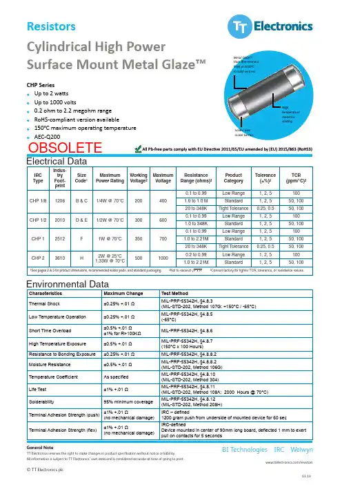
T elephone: 361 992 7900 • Facsimile: 361 992 3377 • Website: Electrical DataIRC TypeIndus-try Foot-print Size Code 1Maximum Power RatingWorking Voltage²Maximum Voltage Resistance Range (ohms)³Product Category Tolerance (±%)³TCR (ppm/°C)³CHP 1/81206B &C 1/4W @ 70°C 2004000.1 to 0.99Low Range 1, 2, 51001.0 to 1.0 M Standard 1, 2, 550, 10020 to 348K Tight T olerance 0.25, 0.550, 100CHP 1/22010 D & E 1/2W @ 70°C 3006000.1 to 0.99Low Range 1, 2, 51001.0 to 348K Standard 1, 2, 550, 100CHP 12512F 1W @ 70°C 3507000.1 to 0.99Low Range 1, 2, 51001.0 to 2.21M Standard 1, 2, 550, 10020 to 348K Tight T olerance 0.25, 0.550, 100CHP 23610H2W @ 25°C 1.33W @ 70°C50010000.2 to 0.99Low Range 1, 2, 51001.0 to 2.21MStandard1, 2, 550, 100¹See pages 2 & 3 for product dimensions, recommended solder pads, and standard packaging. ²Not to exceed P x R ³Consult factory for tighter TCR, tolerance, or resistance values.√CHP Se ries Issue March 2011 Sheet 1 of 3thick film element fired at 1000°C to solid ceramicHightemperature dielectric coatingGeneral Note TT Electronics reserves the right to make changes in product specification without notice or liability.All information is subject to TT Electronics’ own data and is considered accurate at time of going to print.© TT Electronics plc/resistorsBI Technologies IRC WelwynCylindrical High PowerSurface Mount Metal Glaze™CHP SeriesOBSOLETEIRC Type Size Code Industry Footprint Reel Diameter*Quantity Per Reel Carrier Tape WidthComponentPitchCHP 1/8MRC 1/2 B C 12067″2,500 max.8mm 4mm 13″10,000 max.CHP 1/2MRC 1 D E 20107″1,500 max.12mm 4mm 13″5,000 max.CHP 1F 25127″1,500 max.12mm 4mm 13″5,000 max.CHP 2H361013″1,500 max.24mm4mm*The 13″ reel is considered standard and will be supplied unless otherwise specifi ed.Sample Part No.IRC Type(CHP 1/8, CHP 1/2, CHP 1, or CHP 2)Temperature Coeffi cient(50 ppm, 100 ppm)Resistance Value(100 ohms and greater - First 3 signifi cant digits plus 4th digit multiplier)Example: 100 ohms = 1000, 1000 ohms = 1001, 150,000 ohms = 1503(Less than 100 ohms - "R" is used to designate decimal)Example: 51 ohms = 51R0, 1 ohm = 1R00, 0.25 ohms = R250Tolerance(C = 0.25%, D = 0.5%, F = 1.0%; G = 2.0%; J = 5.0%)Packaging Code*(BLK = Bulk, 7 = 7" Reel, 13 = 13" Reel)Lead Free ConstructionOrdering DataCHP 1 - 100 2203 F 13 LF30 40 50 60 70 80 90 100 110 120 130 140 150% o f R a t e d P o w e rAmbient Temperature (°C)Power Derating CurveRepetitive Surge Curve0.0001 0.0010 0.0100 0.1000 1.0000.1msec 1msec 10msec 100msec 10000msecP e a k P o w e r (w a t t s )Surge or Pulse Duration (seconds)Note: Use for repetitive pulses where the average power dissipation is not to exceed the component rating at 70°C. Surge handling capacity for low-repetitive surges may be signifi cantly greater than shown above.Contact factory for recommendations.Standard Reel Packaging per EIA-481:Cylindrical High PowerSurface Mount Metal Glaze™CHP SeriesOBSOLETEOrdering ProcedureThis product has two valid part numbers:European (Welwyn)Part Number:CHP1-220KFI (CHP1 with TCR ±100ppm/°C at 220 kilohms ±1%,Pb-free)USA (IRC)Part Number: CHP11002203FLF (CHP1 with TCR ±100ppm/°C at 220 kilohms ±1%,Pb-free)L F5Cylindrical High PowerSurface Mount Metal Glaze™CHP SeriesOBSOLETE。
派利斯电子(北京)有限公司用户手册TM系列振动变送保护表地震式传感器->壳振涡流探头->轴位移涡流探头->轴振涡流探头->转速目录TM系列振动变送保护表的介绍I.旋转机械监测和保护的发展II.新功能III.通用特点系列振动变送保护表选项TM101机壳振动速度、加速度、位移变送保护表I.概述振动变送保护表的技术参数III.订货选项.IV.现场接线图V.现场报警调试VI.现场操作标定(仅专业工程师操作)TM201轴振动保护表I.概述振动变送表技术说明III.订货选项.IV.现场接线图V.现场安装VI.现场操作标定(专业工程师操作)TM202轴振动保护表I.概述轴位置变送表技术说明III.订货指南IV.现场接线图V.安装VI.现场操作VII.标定程序(专业工程师操作) TM301振动变送监测表I.概述振动变送表技术说明III.订货指南.IV.现场接线图.V.现场安装VI.现场操作标定(专业工程师操作)TM302位移变送保护表I.概述轴位置变送表技术说明III.订货指南.IV.安装V.现场接线图.VI.现场操作VII.标定程序(专业工程师操作) TM401双线轴振动变送表I.概述振动变送表技术指标III.订货指南IV.现场接线图.V.现场安装VI.现场操作标定TM402双线轴位置变送表I.概述技术指标III.订货指南.IV.现场接线图.V.现场安装VI.现场操作VII.标定程序(专业工程师操作) TM501转速/键相变送监测表I.概述振动变送表技术指标III.订货指南IV.现场接线图.V.现场安装VI.现场操作VII.标定步骤TM900电源变换器I.概述技术指标TM0200单通道显示器I.技术指标II.定货指南:TM系列振动变送保护表的介绍I.旋转机械监测和保护的发展旋转机械监测的概念是二战以后由军方实验室推广而来,研究表明机械的故障严重影响生产,振动保护和状态监测的研究从50年代初至今已经得到完善的发展。
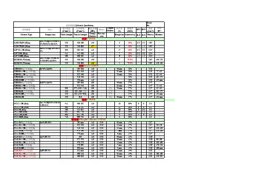
WT-TM201糊状易流动型钙锌复合热稳定剂(高透明型)Paste type liquid Ca/Zn complex heat stabilizer (high transparent type)白色或微黄色糊状物≤2.5≥30静态稳定实验(T=185℃):用户须知:一、本说产品资料仅供参考,由于客户生产配方、加工条件以及工艺等不尽相同,因此我们不做任何承诺。
如您有任何使用或技术问题,请与我公司联系;二、售出的产品与样品质量的一致性,用户对我公司的产品有责任进行检验;三、我们有权对产品进行改进,其规格有任何改动,恕不提前通知。
WT-TM201-1高效型粉状钙锌复合热稳定剂(透明型)Efficient powdered Ca/Zn complex heat stabilizer (transparent)白色粉末≤2.5≥50配方表:用户须知:一、本说产品资料仅供参考,由于客户生产配方、加工条件以及工艺等不尽相同,因此我们不做任何承诺。
如您有任何使用或技术问题,请与我公司联系;二、售出的产品与样品质量的一致性,用户对我公司的产品有责任进行检验;三、我们有权对产品进行改进,其规格有任何改动,恕不提前通知。
WT-TM202糊状易流动型钙锌复合热稳定剂(长效稳定型)Paste type liquid Ca/Zn complex heat stabilizer (long-term stable)白色或微黄色糊状物静态稳定实验(T=185℃):用户须知:一、本说产品资料仅供参考,由于客户生产配方、加工条件以及工艺等不尽相同,因此我们不做任何承诺。
如您有任何使用或技术问题,请与我公司联系;二、售出的产品与样品质量的一致性,用户对我公司的产品有责任进行检验;三、我们有权对产品进行改进,其规格有任何改动,恕不提前通知。
WT-TM101-1粉状硬质钙锌复合热稳定剂(白色制品型)Hard Ca/Zn complex heat stabilizer(white products type)外观白色粉状加热减量(%)≤2.5静态稳定时间(min)≥60无毒无味;经SGS检验符合EN71标准,EN1122标准,EPA 3050B, 美国食品卫生法21CFR、172 888等世界各国一系列环保标准。