SG3525中文使用手册
- 格式:pdf
- 大小:1.99 MB
- 文档页数:5
SG3525说明书SG3525脉宽调制型控制器是美国通用电气公司的产品,作为SG3524的改进型,更适合于运用MOS 管作为开关器件的DC/DC变换器,它是采用双级型工艺制作的新型模拟数字混合集成电路,性能优异,所需外围器件较少。
它的主要特点是:输出级采用推挽输出,双通道输出,占空比0—50%可调.每一通道的驱动电流最大值可达200mA,灌拉电流峰值可达500mA.可直接驱动功率MOS管,工作频率高达400KHz,具有欠压锁定、过压保护和软启动等功能。
该电路由基准电压源、震荡器、误差放大器、PWM比较器与锁存器、分相器、欠压锁定输出驱动级,软启动及关断电路等组成,可正常工作的温度范围是0-700C。
基准电压为5.1 V士1%,工作电压范围很宽,为8V到35V。
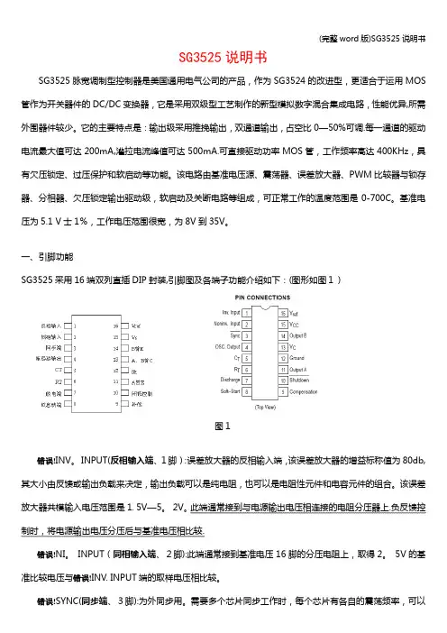
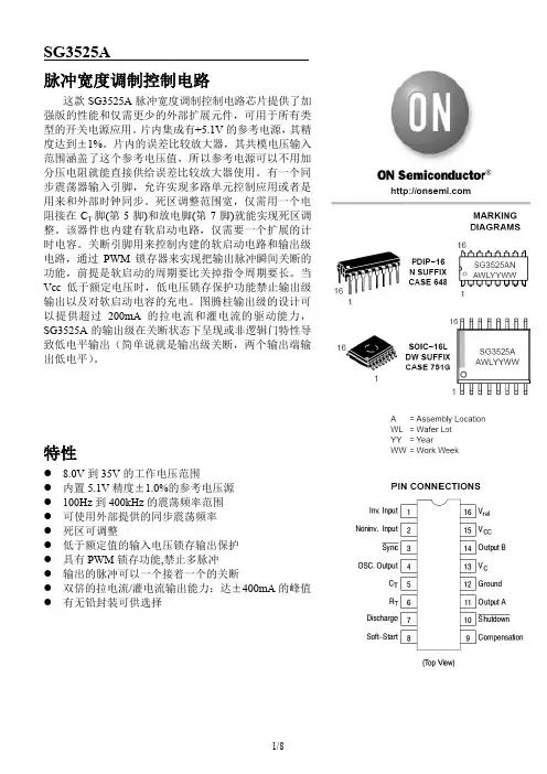
一、引脚功能SG3525采用16端双列直插DIP封装,引脚图及各端子功能介绍如下:(图形如图1)图1错误!INV。
INPUT(反相输入端、1脚):误差放大器的反相输入端,该误差放大器的增益标称值为80db,其大小由反馈或输出负载来决定,输出负载可以是纯电阻,也可以是电阻性元件和电容元件的组合。
该误差放大器共模输入电压范围是1. 5V—5。
2V。
此端通常接到与电源输出电压相连接的电阻分压器上.负反馈控制时,将电源输出电压分压后与基准电压相比较.错误!NI。
INPUT(同相输入端、2脚):此端通常接到基准电压16脚的分压电阻上,取得2。
5V的基准比较电压与错误!INV. INPUT端的取样电压相比较。
错误!SYNC(同步端、3脚):为外同步用。
需要多个芯片同步工作时,每个芯片有各自的震荡频率,可以分别他们的4脚和3脚相连,这时所有芯片的工作频率以最快的芯片工作频率同步。
也可以使单个芯片以外部时钟频率工作。
错误!OSC。
OUTPUT(同步输出端、4脚):同步脉冲输出。
作为多个芯片同步工作时使用.但几个芯片的工作频率不能相差太大,同步脉冲频率应比震荡频率低一些.如不需多个芯片同步工作时,3脚和4脚悬空。

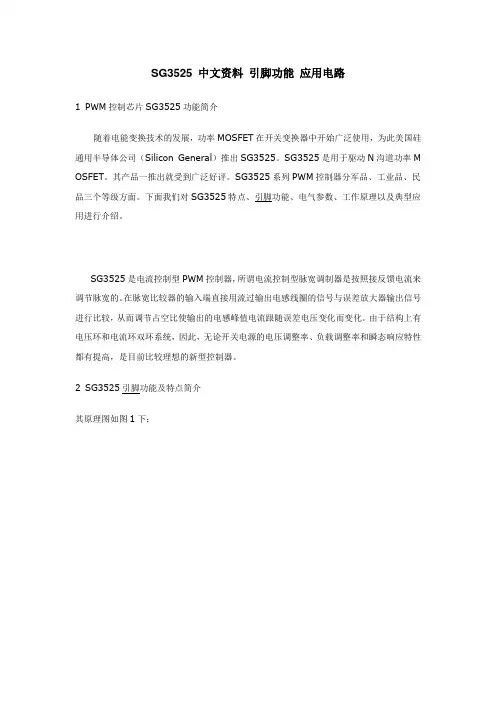
SG3525 中文资料引脚功能应用电路1 PWM控制芯片SG3525功能简介随着电能变换技术的发展,功率MOSFET在开关变换器中开始广泛使用,为此美国硅通用半导体公司(Silicon General)推出SG3525。
SG3525是用于驱动N沟道功率M OSFET。
其产品一推出就受到广泛好评。
SG3525系列PWM控制器分军品、工业品、民品三个等级方面。
下面我们对SG3525特点、引脚功能、电气参数、工作原理以及典型应用进行介绍。
SG3525是电流控制型PWM控制器,所谓电流控制型脉宽调制器是按照接反馈电流来调节脉宽的。
在脉宽比较器的输入端直接用流过输出电感线圈的信号与误差放大器输出信号进行比较,从而调节占空比使输出的电感峰值电流跟随误差电压变化而变化。
由于结构上有电压环和电流环双环系统,因此,无论开关电源的电压调整率、负载调整率和瞬态响应特性都有提高,是目前比较理想的新型控制器。
2 SG3525引脚功能及特点简介其原理图如图1下:图1 SG3525内部电路图图2 SG3525引脚图1.Inv.input(引脚1):误差放大器反向输入端。
在闭环系统中,该引脚接反馈信号。
在开环系统中,该端与补偿信号输入端(引脚9)相连,可构成跟随器。
2.Noninv.input(引脚2):误差放大器同向输入端。
在闭环系统和开环系统中,该端接给定信号。
根据需要,在该端与补偿信号输入端(引脚9)之间接入不同类型的反馈网络,可以构成比例、比例积分和积分等类型的调节器。
3.Sync(引脚3):振荡器外接同步信号输入端。
该端接外部同步脉冲信号可实现与外电路同步。
4.OSC.Output(引脚4):振荡器输出端。
5.CT(引脚5):振荡器定时电容接入端。
6.RT(引脚6):振荡器定时电阻接入端。
7.Discharge(引脚7):振荡器放电端。
该端与引脚5之间外接一只放电电阻,构成放电回路。
8.Soft-Start(引脚8):软启动电容接入端。
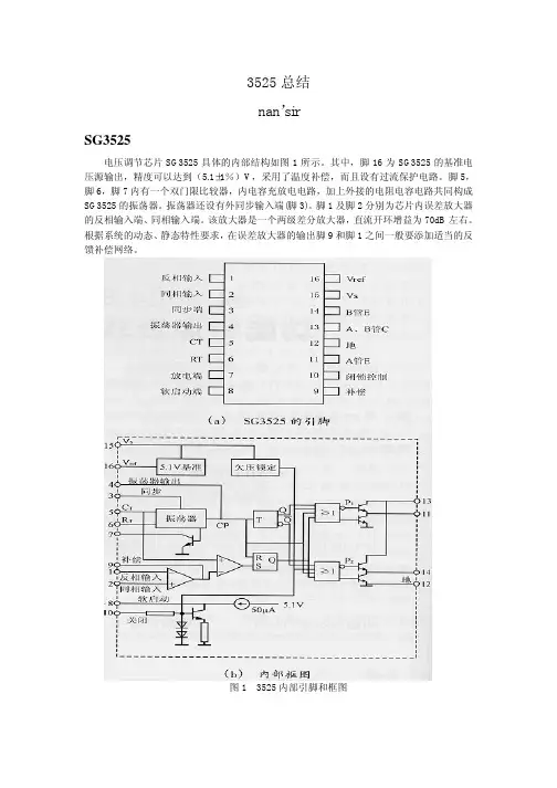
3525总结nan’sirSG3525电压调节芯片SG3525具体的内部结构如图1所示。
其中,脚16为SG3525的基准电压源输出,精度可以达到(5.1±1%)V,采用了温度补偿,而且设有过流保护电路。
脚5,脚6,脚7内有一个双门限比较器,内电容充放电电路,加上外接的电阻电容电路共同构成SG3525的振荡器。
振荡器还设有外同步输入端(脚3)。
脚1及脚2分别为芯片内误差放大器的反相输入端、同相输入端。
该放大器是一个两级差分放大器,直流开环增益为70dB左右。
根据系统的动态、静态特性要求,在误差放大器的输出脚9和脚1之间一般要添加适当的反馈补偿网络。
图1 3525内部引脚和框图1. 下面分别阐述其各部分功能:a 基准电压源: 基准电压源是一个三端稳压电路,其输入电压V CC 可在(8~35)V 内变化,通常采用+15V ,其输出电压V ST =5.1V ,精度%1±,采用温度补偿,作为芯片内部电路的电源,也可为芯片外围电路提供标准电源,向外输出电流可达400mA ,没有过流保护电路。
b 振荡电路: 由一个双门限电压均从基准电源取得,其高门限电压V V H 9.3=低门限电压V V L 9.0=,内部横流源向C T 充电,其端压V C 线性上升,构成锯齿波的上升沿,当H C V V =时比较器动作,充电过程结束,上升时间t 1为:T T C R t 67.01=比较器动作时使放电电路接通,C T 放电,V C 下降并形成锯齿波的下降沿,当L C V V =时比较器动作,放电过程结束,完成一个工作循环,下降时间间t 2为:T D C R t 3.12=注意:此时间即为死区时间 锯齿波的基本周期T 为:()T D T C R R t t T 3.167.021+=+=因为T D R R <<⇒12t t <<由上可见锯齿波的上升沿远长于下降沿,因此上升沿作为工作沿,下降沿作为回扫沿。
SG3525中文资料1.1.3 SG3524与SG3524主要区别作为SG3524的增强版本,SG3525在以下方面进行了改进。
1)增加欠电压锁定电路。
当SG3525输入电压低于8V时,控制器内部电路锁定,除基准电源和一些必要电路之外的所有电路停止工作,此时控制器消耗的电流极小。
2)SG3525内部50 的恒流源进行充电。
3)提高了基准电源的精度。
SG3525中基准电源的精度提高了1%,而SG3524中基准电源的精度只有8%。
4)去除了限流比较器。
SG3525去除了SG3524中的限流比较器,改由外部关断信号输入使用中,一般在引脚10上接电流检测信号,如果过电流检测信号维持时间较长,软启动电容将被放电。
5)PWM比较器的反向输入端增加至两个。
在SG3524中,误差放大器输出端、限流比较器输出端和外部关断信号输入电路共用PWM比较器的反向输入端。
在SG3525中对此进行了改进,使误差放大器输出端和外部关断信号输入电路分别送至PWM比较器的一个反向输入端。
这样做的好处在于,避免了误差放大器和外部关断信号输入电路之间相互影响,有利于误差放大器和补偿网络工作精度提高。
6)增加了PWM琐存器。
为了使关断电路更可靠的工作,SG3525在其内部增加了PWM 琐存器。
PWM比较器输出信号首先送至PWM琐存器,琐存器由关断电路置位,由振荡器输出时间脉冲复位。
当关断电路工作时,即使过电流信号立即消失,琐存器也可以维持一个周期的关断控制,直到下一周期时钟信号使琐存器复位为止。
同时,由于PWM琐存器对PWM比较器的置位信号进行琐存,误差放大器上的噪声信号、振铃及其他信号在此过程中都被消除了。
只有在下一个时钟周期才能重新复位,可靠性大大提高。
7)震荡器增加了同步端和放电端。
SG3524中的振荡器只有CT和RT两个引脚,其充电和放电回路是相同的。
在SG3525中的振荡器除了CT和RT两个引脚外,又增加了一个同步端(引脚3RT的阻值决定了内部恒流源对CT充电电流的大小,而CT的放电则由引脚之间的外接电阻决定。
PWM控制芯片SG3525功能简介1.1 PWM控制芯片SG3525功能简介随着电能变换技术的发展,功率MOSFET在开关变换器中开始广泛使用,为此美国硅通用半导体公司(Silicon General)推出SG3525。
SG3525是用于驱动N沟道功率MOSFET。
其产品一推出就受到广泛好评。
SG3525系列PWM控制器分军品、工业品、民品三个等级。
下面我们对SG3525特点、引脚功能、电气参数、工作原理以及典型应用进行介绍。
SG3525是电流控制型PWM控制器,所谓电流控制型脉宽调制器是按照接反馈电流来调节脉宽的。
在脉宽比较器的输入端直接用流过输出电感线圈的信号与误差放大器输出信号进行比较,从而调节占空比使输出的电感峰值电流跟随误差电压变化而变化。
由于结构上有电压环和电流环双环系统,因此,无论开关电源的电压调整率、负载调整率和瞬态响应特性都有提高,是目前比较理想的新型控制器。
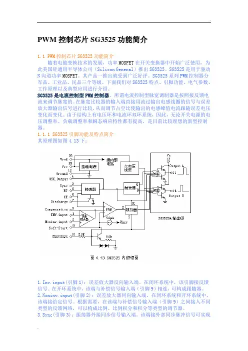
1.1.1 SG3525引脚功能及特点简介其原理图如图4.13下:1.Inv.input(引脚1):误差放大器反向输入端。
在闭环系统中,该引脚接反馈信号。
在开环系统中,该端与补偿信号输入端(引脚9)相连,可构成跟随器。
2.Noninv.input(引脚2):误差放大器同向输入端。
在闭环系统和开环系统中,该端接给定信号。
根据需要,在该端与补偿信号输入端(引脚9)之间接入不同类型的反馈网络,可以构成比例、比例积分和积分等类型的调节器。
3.Sync(引脚3):振荡器外接同步信号输入端。
该端接外部同步脉冲信号可实现与外电路同步。
4.OSC.Output(引脚4):振荡器输出端。
5.CT(引脚5):振荡器定时电容接入端。
6.RT(引脚6):振荡器定时电阻接入端。
7.Discharge(引脚7):振荡器放电端。
该端与引脚5之间外接一只放电电阻,构成放电回路。
8.Soft-Start(引脚8):软启动电容接入端。
该端通常接一只5 的软启动电容。

SG2525ASG3525AREGULATING PULSE WIDTH MODULATORS .8 TO 35 V OPERATION.5.1 V REFERENCE TRIMMED TO ± 1 %.100 Hz TO 500 KHz OSCILLATOR RANGE.SEPARATE OSCILLATOR SYNC TERMINAL.ADJUSTABLE DEADTIME CONTROL.INTERNAL SOFT-START.PULSE-BY-PULSE SHUTDOWN.INPUT UNDERVOLTAGE LOCKOUT WITHHYSTERESIS.LATCHING PWM TO PREVENT MULTIPLEPULSES.DUAL SOURCE/SINK OUTPUT DRIVERSDESCRIPTIONThe SG3525A series of pulse width modulator inte-grated circuits are designed to offer improved per-formance and lowered external parts count when used in designing all types of switching power sup-plies. The on-chip + 5.1 V reference is trimmed to ±1 % and the input common-mode range of the error amplifier includes the reference voltage eliminating external resistors. A sync input to the oscillator al-lows multiple units to be slaved or a single unit to be synchronized to an external system clock. A single resistor between the C T and the discharge terminals provide a wide range of dead time ad- justment. These devices also feature built-in soft-start circuitry with only an external timing capacitor required. A shutdown terminal controls both the soft-start circu-ity and the output stages, providing instantaneousturn off through the PWM latch with pulsed shut-down, as well as soft-start recycle with longer shut-down commands. These functions are also control-led by an undervoltage lockout which keeps the out-puts off and the soft-start capacitor discharged for sub-normal input voltages. This lockout circuitry in-cludes approximately 500 mV of hysteresis for jitter-free operation. Another feature of these PWM cir-cuits is a latch following the comparator. Once a PWM pulses has been terminated for any reason, the outputs will remain off for the duration of the pe-riod. The latch is reset with each clock pulse. The output stages are totem-pole designs capable of sourcing or sinking in excess of 200 mA. The SG3525A output stage features NOR logic, giving a LOW output for an OFF state.DIP16 16(Narrow)Type Plastic DIP SO16SG2525A SG2525AN SG2525APSG3525A SG3525AN SG3525APPIN CONNECTIONS AND ORDERING NUMBERS (top view)®June 20001/12ABSOLUTE MAXIMUM RATINGSSymbol Parameter Value Unit V i Supply Voltage40V V C Collector Supply Voltage40VI OSC Oscillator Charging Current5mAI o Output Current, Source or Sink500mAI R Reference Output Current50mAI T Current through C T TerminalLogic InputsAnalog Inputs5– 0.3 to + 5.5– 0.3 to V imAVVP tot Total Power Dissipation at T amb = 70 °C1000mW T j Junction Temperature Range– 55 to 150°C T stg Storage Temperature Range– 65 to 150°CT op Operating Ambient Temperature : SG2525A SG3525A – 25 to 850 to 70°C°CTHERMAL DATASymbol Parameter SO16DIP16UnitR th j-pins R th j-amb R th j-alumina Thermal Resistance Junction-pins MaxThermal Resistance Junction-ambient MaxThermal Resistance Junction-alumina (*) Max505080°C/W°C/W°C/W*Thermal resistance junction-alumina with the device soldered on the middle of an alumina supporting substrate measuring 15 × 20 mm ; 0.65 mm thickness with infinite heatsink.BLOCK DIAGRAMELECTRICAL CHARACTERISTICS(V# i = 20 V, and over operating temperature, unless otherwise specified)Symbol Parameter TestConditions SG2525A SG3525AUnitMin. Typ. Max. Min. Typ. Max. REFERENCE SECTIONV REF Output Voltage T j = 25 °C 5.05 5.1 5.155 5.1 5.2V ∆V REF Line Regulation V i = 8 to 35 V10201020mV ∆V REF Load Regulation I L = 0 to 20 mA20502050mV ∆V REF/∆T*Temp. Stability Over Operating Range20502050mV*Total Output Variation Line, Load andTemperature5 5.2 4.95 5.25VShort Circuit Current V REF = 0 T j = 25 °C8010080100mA *Output Noise Voltage10 Hz ≤f ≤ 10 kHz,T j = 25 °C4020040200µVrms∆V REF*Long Term Stability T j = 125 °C, 1000 hrs20502050mV OSCILLATOR SECTION * **, •Initial Accuracy T j = 25 °C± 2± 6± 2±6% *, •Voltage Stability V i = 8 to 35 V± 0.3± 1± 1±2%∆f/∆T*Temperature Stability Over Operating Range± 3± 6± 3±6%f MIN Minimum Frequency R T = 200 KΩ C T = 0.1 µF120120Hzf MAX Maximum Frequency R T = 2 KΩ C T = 470 pF400400KHzCurrent Mirror I RT = 2 mA 1.72 2.2 1.72 2.2mA *, •Clock Amplitude3 3.53 3.5V *, •Clock Width T j = 25 °C0.30.510.30.51µs Sync Threshold 1.22 2.8 1.22 2.8VSync Input Current Sync Voltage = 3.5 V1 2.51 2.5mA ERROR AMPLIFIER SECTION (V CM = 5.1 V)V OS Input Offset Voltage 0.55210mVI b Input Bias Current110110µAI os Input Offset Current11µADC Open Loop Gain R L≥ 10 MΩ60756075dB *Gain BandwidthProductG v = 0 dB T j = 25 °C1212MHz*, DC Transconduct.30 KΩ≤ R L≤ 1 MΩT j = 25 °C1.1 1.5 1.1 1.5msOutput Low Level0.20.50.20.5VOutput High Level 3.8 5.6 3.8 5.6V CMR Comm. Mode Reject.V CM = 1.5 to 5.2 V60756075dB PSR Supply VoltageRejectionV i = 8 to 35 V50605060dBELECTRICAL CHARACTERISTICS (continued)Symbol Parameter TestConditions SG2525A SG3525AUnitMin. Typ. Max. Min. Typ. Max.PWM COMPARATORMinimum Duty-cycle00%•Maximum Duty-cycle45494549%•Input Threshold Zero Duty-cycle0.70.90.70.9VMaximum Duty-cycle 3.3 3.6 3.3 3.6V *Input Bias Current0.0510.051µA SHUTDOWN SECTIONSoft Start Current V SD = 0 V, V SS=0V255080255080µASoft Start Low Level V SD = 2.5 V0.40.70.40.7VShutdown Threshold To outputs, V SS = 5.1 VT j = 25 °C0.60.810.60.81VShutdown Input Current V SD = 2.5 V0.410.41mA *Shutdown Delay V SD = 2.5 V T j = 25 °C0.20.50.20.5µs OUTPUT DRIVERS (each output) (V C = 20 V)Output Low Level I sink = 20 mA0.20.40.20.4VI sink = 100 mA1212VOutput High Level I source = 20 mA18191819VI source = 100 mA17181718VUnder-Voltage Lockout V comp and V ss=High678678VI C Collector Leakage V C = 35 V200200µAt r*Rise Time C L = 1 nF, T j = 25 °C100600100600ns t f*Fall Time C L = 1 nF, T j = 25 °C5030050300ns TOTAL STANDBY CURRENTI s Supply Current V i = 35 V14201420mA*These parameters, although guaranteed over the recommended operating conditions, are not 100 % tested in production.•Tested at f osc = 40 KHz (R T = 3.6 KΩ, C T = 10nF, R D = 0 Ω). Approximate oscillator frequency is defined by :1f =C T (0.7 R T + 3 R D).DC transconductance (g M) relates to DC open-loop voltage gain (G v) according to the following equation : G v = g M R L where R L is the resistance from pin 9 to ground. The minimum g M specification is used to calculate minimum G vwhen the error amplifier output is loaded.TEST CIRCUITFigure 1 : Oscillator Charge Time vs. R T and C T .Figure 2 : Oscillator Discharge Time vs. R D and C T.RECOMMENDED OPERATING CONDITIONS (•)ParameterValue Input Voltage (V i )8 to 35 V Collector Supply Voltage (V C )4.5 to 35 V Sink/Source Load Current (steady state)0 to 100 mA Sink/Source Load Current (peak)0 to 400 mA Reference Load Current 0 to 20 mA Oscillator Frequency Range 100 Hz to 400 KHz Oscillator Timing Resistor 2 K Ω to 150 K ΩOscillator Timing Capacitor 0.001 µF to 0.1 µFDead Time Resistor Range0 to 500 Ω(⋅)Range over which the device is functional and parameter limits are guaranteed.Figure 3 : Output Saturation Characteristics.Figure 4 : Error Amplifier Voltage Gain andPhase vs. Frequency.SHUTDOWN OPTIONS (see Block Diagram) Since both the compensation and soft-start termi-nals (Pins 9 and 8) have current source pull-ups, either can readily accept a pull-down signal which only has to sink a maximum of 100 µA to turn off the outputs. This is subject to the added requirement of discharging whatever external capacitance may be attached to these pins.An alternate approach is the use of the shutdown cir-cuitry of Pin 10 which has been improved to en-hance the available shutdown options. Activating this circuit by applying a positive signal on Pin 10 performs two functions : the PWM latch is immedi-ately set providing the fastest turn-off signal to the outputs ; and a 150 µA current sink begins to dis-charge the external soft-start capacitor. If the shut-down command is short, the PWM signal is termi-nated without significant discharge of the soft-start capacitor, thus, allowing, for example, a convenient implementation of pulse-by-pulse current limiting. Holding Pin 10 high for a longer duration, however, will ultimately discharge this external capacitor, re-cycling slow turn-on upon release.Pin 10 should not be left floating as noise pickup could conceivably interrupt normal operation.Figure 5: Error Amplifier.PRINCIPLES OF OPERATIONFigure 6: Oscillator Schematic.Figure 7 : Output Circuit (1/2 circuit shown).Figure 10.Figure 11.For single-ended supplies, the driver outputs are grounded. The V C terminal is switched to ground by the totem-pole source transistors on alternate oscil-lator cycles.In conventional push-pull bipolar designs, forward base drive is controlled by R 1 - R 3. Rapid turn-off times for the power devices are achieved with speed-up capacitors C 1 and C 2.The low source impedance of the output drivers pro-vides rapid charging of Power Mos input capaci-tance while minimizing external components.Low power transformers can be driven directly.Automatic reset occurs during dead time, when both ends of the primary winding are switched to ground.Figure 8.Figure 9.DIP16DIM.mm inch MIN.TYP.MAX.MIN.TYP.MAX.a10.510.020B 0.771.650.0300.065b 0.50.020b10.250.010D 200.787E 8.50.335e 2.540.100e317.780.700F 7.10.280I 5.10.201L 3.30.130Z1.270.050OUTLINE ANDMECHANICAL DATASO16 NarrowDIM.mm inch MIN.TYP.MAX.MIN.TYP.MAX.A1.750.069a10.10.250.0040.009a21.60.063b0.350.460.0140.018b10.190.250.0070.010C0.50.020c145˚ (typ.)D (1)9.8100.3860.394E5.86.20.2280.244e1.270.050e38.890.350F (1)3.840.1500.157G4.65.30.1810.209L0.4 1.270.0160.050M0.620.024S (1) D and F do not include mold flash or protrusions. Mold flash or potrusions shall not exceed 0.15mm (.006inch).OUTLINE AND MECHANICAL DATA8˚(max.)Information furnished is believed to be accurate and reliable. However, STMicroelectronics assumes no responsibility for the conse-quences of use of such information nor for any infringement of patents or other rights of third parties which may result from its use. No license is granted by implication or otherwise under any patent or patent rights of STMicroelectronics. Specification mentioned in this publication are subject to change without notice. This publication supersedes and replaces all information previously supplied. STMi-croelectronics products are not authorized for use as critical components in life support devices or systems without express written approval of STMicroelectronics.The ST logo is a registered trademark of STMicroelectronics© 2000 STMicroelectronics – Printed in Italy – All Rights ReservedSTMicroelectronics GROUP OF COMPANIESAustralia - Brazil - China - Finland - France - Germany - Hong Kong - India - Italy - Japan - Malaysia - Malta - Morocco -Singapore - Spain - Sweden - Switzerland - United Kingdom - U.S.A.。
SG3525 中文资料引脚功能应用电路1 PWM控制芯片SG3525功能简介随着电能变换技术的发展,功率MOSFET在开关变换器中开始广泛使用,为此美国硅通用半导体公司(Silicon General)推出SG3525。
SG3525是用于驱动N沟道功率M OSFET。
其产品一推出就受到广泛好评。
SG3525系列PWM控制器分军品、工业品、民品三个等级方面。
下面我们对SG3525特点、引脚功能、电气参数、工作原理以及典型应用进行介绍。
SG3525是电流控制型PWM控制器,所谓电流控制型脉宽调制器是按照接反馈电流来调节脉宽的。
在脉宽比较器的输入端直接用流过输出电感线圈的信号与误差放大器输出信号进行比较,从而调节占空比使输出的电感峰值电流跟随误差电压变化而变化。
由于结构上有电压环和电流环双环系统,因此,无论开关电源的电压调整率、负载调整率和瞬态响应特性都有提高,是目前比较理想的新型控制器。
2 SG3525引脚功能及特点简介其原理图如图1下:图1 SG3525内部电路图图2 SG3525引脚图1.Inv.input(引脚1):误差放大器反向输入端。
在闭环系统中,该引脚接反馈信号。
在开环系统中,该端与补偿信号输入端(引脚9)相连,可构成跟随器。
2.Noninv.input(引脚2):误差放大器同向输入端。
在闭环系统和开环系统中,该端接给定信号。
根据需要,在该端与补偿信号输入端(引脚9)之间接入不同类型的反馈网络,可以构成比例、比例积分和积分等类型的调节器。
3.Sync(引脚3):振荡器外接同步信号输入端。
该端接外部同步脉冲信号可实现与外电路同步。
4.OSC.Output(引脚4):振荡器输出端。
5.CT(引脚5):振荡器定时电容接入端。
6.RT(引脚6):振荡器定时电阻接入端。
7.Discharge(引脚7):振荡器放电端。
该端与引脚5之间外接一只放电电阻,构成放电回路。
8.Soft-Start(引脚8):软启动电容接入端。
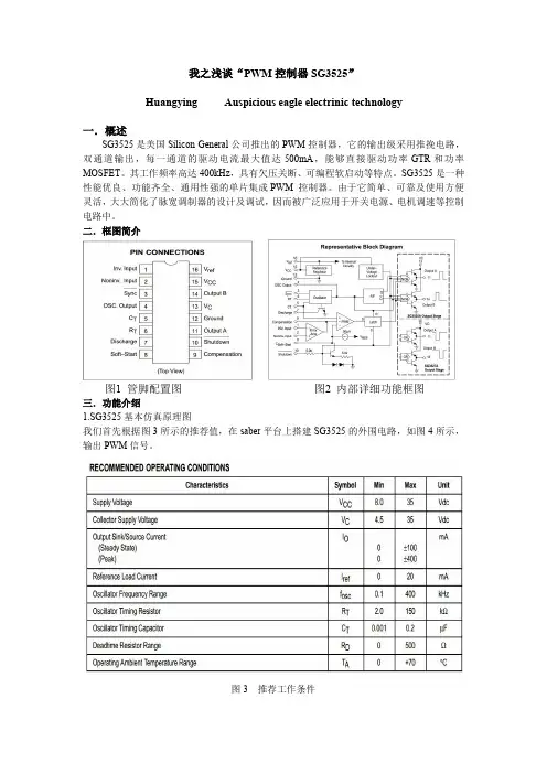
我之浅谈“PWM控制器SG3525”Huangying Auspicious eagle electrinic technology一.概述SG3525是美国Silicon General公司推出的PWM控制器,它的输出级采用推挽电路,双通道输出,每一通道的驱动电流最大值达500mA,能够直接驱动功率GTR和功率MOSFET。
其工作频率高达400kHz,具有欠压关断、可编程软启动等特点。
SG3525是一种性能优良、功能齐全、通用性强的单片集成PWM控制器。
由于它简单、可靠及使用方便灵活,大大简化了脉宽调制器的设计及调试,因而被广泛应用于开关电源、电机调速等控制电路中。
二.框图简介图1管脚配置图图2内部详细功能框图三.功能介绍1.SG3525基本仿真原理图我们首先根据图3所示的推荐值,在saber平台上搭建SG3525的外围电路,如图4所示,输出PWM信号。
图3推荐工作条件图4SG3525PWM输出的基本电路执行Transient运行后,得到PWM信号,如下图5所示图5SG3525输出PWM信号图四.分析通过以上的简单介绍后,要想深入地理解和应用SG3525,我们需要弄明白以下几个问题:1)满足什么条件后,SG3525能正常工作?2)SG3525内部震荡信号频率fos,振荡器向外输出频率fosout,和pwm开关频率fs之间存在什么数量关系,各自频率大小分别由什么参数决定?3)输出2路pwm信号之间的死区时间是什么?死区时间大小由什么参数决定?4)输出PWM信号的幅度,由什么决定?5)如果检测到外部故障,如何锁闭PWM输出信号?五.解决疑问问题:1)满足什么条件后,SG3525能正常工作?分析:SG3525是单片集成的PWM信号控制芯片,和其他芯片一样,需要满足基本的两个原始条件:a.能源:即提供供电,如图4中的Vin,Vref,VC;b.时钟:就是振荡器要正常起振,如图4中的Rt,Ct构成外部振荡器;仿真如下图6和图7所示:图6图7如图6,只接了电源和振荡器,SG3525能工作,并且能够输出PWM信号(细心的你可能已经发现PWM信号不是常见的方波,而是尖脉冲信号。
SG3525中文资料引脚图应用电路图 (1)简介:SG3525中文资料引脚图应用电路图随着电能变换技术的发展,功率MOSFET在开关变换器中开始广泛使用。
为此,美国硅通用半导体公司推出了SG3525,以用于驱动 ... 关键字:SG3525SG3525中文资料引脚图应用电路图随着电能变换技术的发展,功率MOSFET在开关变换器中开始广泛使用。
为此,美国硅通用半导体公司推出了SG3525,以用于驱动N沟道功率MOSFET。
SG3525是一种性能优良、功能齐全和通用性强的单片集成PWM控制芯片,它简单可靠及使用方便灵活,输出驱动为推拉输出形式,增加了驱动能力;内部含有欠压锁定电路、软启动控制电路、PWM锁存器,有过流保护功能,频率可调,同时能限制最大占空比。
其性能特点如下:1)工作电压范围宽: 8~35V。
2)内置5.1 V±1.0%的基准电压源。
3)芯片内振荡器工作频率宽100Hz~400 kHz。
4)具有振荡器外部同步功能。
5)死区时间可调。
为了适应驱动快速场效应管的需要,末级采用推拉式工作电路,使开关速度更陕,末级输出或吸入电流最大值可达400mA。
6)内设欠压锁定电路。
当输入电压小于8V时芯片内部锁定,停止工作(基准源及必要电路除外),使消耗电流降至小于2mA。
7)有软启动电路。
比较器的反相输入端即软启动控制端芯片的引脚8,可外接软启动电容。
该电容器内部的基准电压Uref由恒流源供电,达到2.5V的时间为t=(2.5V/50μA)C,占空比由小到大(50%)变化。
8)内置PWM(脉宽调制)。
锁存器将比较器送来的所有的跳动和振荡信号消除。
只有在下一个时钟周期才能重新置位,系统的可靠性高。
l 脉宽调制器SG3525简介1.1 结构框图SG3525是定频PWM电路,采用原理16引脚标准DIP封装。
其各引脚功能如图1所示,内部原理框图如图2所示。
1.2 引脚功能说明直流电源Vs从脚15接入后分两路,一路加到或非门;另一路送到基准电压稳压器的输入端,产生稳定的元器件作为电源。
s g3525中文资料摘要:对PWM控制芯片SG3524与SG3525的工作性能作了介绍和比较,通过实验得出了SG3525在软起动功能上较SG3524有很大的改进。
关键词:SG3524;SG3525;脉宽调制;软起动0 引言:目前,开关电源越来越广泛地应用于各行各业中,是各种用电设备的重要组成部分。
在开关电源的设计过程中,常常使用各种PWM的IC。
因此,作为开关电源的设计者,有必要熟悉各种PWM的集成芯片的性能差别,才能在设计的时候灵活应用。
下面主要针对常用的SG3524与SG3525两种芯片进行对比分析。
1 SG3524与SG3525:SG3524是定频PWM电路,采用16引脚标准DIP封装。
其各引脚功能如图1(a)所示,内部框图如图1(b)所示。
(a)SG3524的引脚(b)内部框图图1 SG3524引脚及内部框图脚9可以通过对地接阻容网络,补偿系统的幅频和相频响应特性。
根据试验结果,对地接电容就可以实现软起动功能。
SG3525也是定频PWM电路,采用16引脚标准DIP封装。
其各引脚功能如图2(a)所示,内部框图如图2(b)所示。
脚8为软起动端。
(a)SG3525的引脚(b)内部框图图2 SG3525引脚及内部框图2 SG3525相对SG3524的改进:SG3525在SG3524的基础上,主要作了以下改进。
1)增设欠压锁定电路电路主要作用是当IC输入电压<8V时,集成块内部电路锁定,停止工作(基准源及必要电路除外),使之消耗电流降至很小(约2mA)。
2)有软起动电路比较器的反相端即软起动控制端脚8可外接软起动电容。
该电容由内部5V基准参考电压的50μA恒流源充电,使占空比由小到大(50%)变化。
3)比较器有两个反相输入端 SG3524的误差放大器、电流控制器和关闭控制3个信号共用一个反相输入端,现改为增加一个反相输入端,误差放大器与关闭电路各自送至比较器的反相端。
这样,便避免了彼此相互影响,有利于误差放大器和补偿网络工作精度的提高。
SG3525A图片1.典型逻辑框图订购信息SG3525A最大额定值超过最大额定值器件会被损坏。
最大额定用于界定器件个体的耐受度限制值(非正常的运行条件),对于每个器件该值并不统一。
一旦超过改值,器件的功能和运行是未知的,器件会损坏或者可靠性受到影响。
1. 环境温度高于﹢50℃时,递减10mW/℃。
2. 环境温度高于﹢25℃时,递减,16mW/℃。
推荐运行条件引脚;一个150uA 的放电路径被打开来给外部软启动电容放电。
如果关断命令持续时间较短,PWM 信号输出会终止而不会给软启动电容放电,因此,允许,例如方便实现逐个脉冲的电流限制。
让第10引脚维持一段长时间的高电平,就会基本上放光外部软启动电容的电荷,导致重新上电的周期变慢。
第10脚不能浮空,因为开关噪声可能会中断器件的应用信息关断操作(见第2页逻辑图) 因为补偿端(第9脚)和软启动端(第8脚)能被电流源上拉,这两端中的任意一端都能够轻易承受一个最大仅需要100uA 的电流下拉信号就能使输出关闭。
这就意味着需要增加外部电容连接到这些脚上。
另一种可替换的方法是,使用第10脚的关断电路引脚,该引脚被改善用来加强关断操作的可靠性。
激活这个3.T low=0℃T high=﹢70℃4.因为每个器件的长期稳定性在出厂前无法测试,这些质量指标只是通过工程采样估算的稳定性平均值。
5.测试频率为f osc=40kHz (R T=3.6kΩ,C T=0.01uF,R D=0Ω)。
6. 由于输出脉冲极性,只是用到SG3525A做测试。
图片2.实验室测试原理图SG3525A图片3.振荡器充电时间Vs R T图片4.振荡器放电时间Vs R D图片5.误差放大器开环频率响应图片6.输出饱和特性曲线SG3525A图片9.输出电路(其中的1/2电路)对于单端供电,驱动输出端都接地。
在间隔的震荡周期,V C端被图腾柱源晶体管接通到地。
在传统的双极推挽式设计中,原先的基本驱动是被R1-R3控制的。
PWM控制芯片SG3525功能简介(图)2007-2-28 9:02:58 电源在线1.1 PWM控制芯片SG3525功能简介随着电能变换技术的发展,功率MOSFET在开关变换器中开始广泛使用,为此美国硅通用半导体公司(Silicon General)推出SG3525。
SG3525是用于驱动N沟道功率MOSFET。
其产品一推出就受到广泛好评。
SG3525系列PWM控制器分军品、工业品、民品三个等级。
下面我们对SG3525特点、引脚功能、电气参数、工作原理以及典型应用进行介绍。
SG3525是电流控制型PWM控制器,所谓电流控制型脉宽调制器是按照接反馈电流来调节脉宽的。
在脉宽比较器的输入端直接用流过输出电感线圈的信号与误差放大器输出信号进行比较,从而调节占空比使输出的电感峰值电流跟随误差电压变化而变化。
由于结构上有电压环和电流环双环系统,因此,无论开关电源的电压调整率、负载调整率和瞬态响应特性都有提高,是目前比较理想的新型控制器。
1.1.1 SG3525引脚功能及特点简介其原理图如图4.13下:1.Inv.input(引脚1):误差放大器反向输入端。
在闭环系统中,该引脚接反馈信号。
在开环系统中,该端与补偿信号输入端(引脚9)相连,可构成跟随器。
2.Noninv.input(引脚2):误差放大器同向输入端。
在闭环系统和开环系统中,该端接给定信号。
根据需要,在该端与补偿信号输入端(引脚9)之间接入不同类型的反馈网络,可以构成比例、比例积分和积分等类型的调节器。
3.Sync(引脚3):振荡器外接同步信号输入端。
该端接外部同步脉冲信号可实现与外电路同步。
4.OSC.Output(引脚4):振荡器输出端。
5.CT(引脚5):振荡器定时电容接入端。
6.RT(引脚6):振荡器定时电阻接入端。
7.Discharge(引脚7):振荡器放电端。
该端与引脚5之间外接一只放电电阻,构成放电回路。
8.Soft-Start(引脚8):软启动电容接入端。
PWM控制芯片SG3525功能简介1.1 PWM控制芯片SG3525功能简介随着电能变换技术的发展,功率MOSFET在开关变换器中开始广泛使用,为此美国硅通用半导体公司(Silicon General)推出SG3525。
SG3525是用于驱动N沟道功率MOSFET。
其产品一推出就受到广泛好评。
SG3525系列PWM控制器分军品、工业品、民品三个等级。
下面我们对SG3525特点、引脚功能、电气参数、工作原理以及典型应用进行介绍。
SG3525是电流控制型PWM控制器,所谓电流控制型脉宽调制器是按照接反馈电流来调节脉宽的。
在脉宽比较器的输入端直接用流过输出电感线圈的信号与误差放大器输出信号进行比较,从而调节占空比使输出的电感峰值电流跟随误差电压变化而变化。
由于结构上有电压环和电流环双环系统,因此,无论开关电源的电压调整率、负载调整率和瞬态响应特性都有提高,是目前比较理想的新型控制器。
1.1.1 SG3525引脚功能及特点简介其原理图如图4.13下:1.Inv.input(引脚1):误差放大器反向输入端。
在闭环系统中,该引脚接反馈信号。
在开环系统中,该端与补偿信号输入端(引脚9)相连,可构成跟随器。
2.Noninv.input(引脚2):误差放大器同向输入端。
在闭环系统和开环系统中,该端接给定信号。
根据需要,在该端与补偿信号输入端(引脚9)之间接入不同类型的反馈网络,可以构成比例、比例积分和积分等类型的调节器。
3.Sync(引脚3):振荡器外接同步信号输入端。
该端接外部同步脉冲信号可实现与外电路同步。
4.OSC.Output(引脚4):振荡器输出端。
5.CT(引脚5):振荡器定时电容接入端。
6.RT(引脚6):振荡器定时电阻接入端。
7.Discharge(引脚7):振荡器放电端。
该端与引脚5之间外接一只放电电阻,构成放电回路。
8.Soft-Start(引脚8):软启动电容接入端。
该端通常接一只5 的软启动电容。
SG3525APulse Width Modulator Control CircuitThe SG3525A pulse width modulator control circuit offers improved performance and lower external parts count when implemented for controlling all types of switching power supplies. The on−chip +5.1 V reference is trimmed to "1% and the erroramplifier has an input common−mode voltage range that includes the reference voltage, thus eliminating the need for external divider resistors. A sync input to the oscillator enables multiple units to be slaved or a single unit to be synchronized to an external system clock.A wide range of deadtime can be programmed by a single resistor connected between the C T and Discharge pins. This device also features built−in soft−start circuitry, requiring only an external timing capacitor. A shutdown pin controls both the soft−start circuitry and the output stages, providing instantaneous turn off through the PWM latch with pulsed shutdown, as well as soft−start recycle with longer shutdown commands. The under voltage lockout inhibits the outputs and the changing of the soft−start capacitor when V CC is below nominal. The output stages are totem−pole design capable of sinking and sourcing in excess of 200 mA. The output stage of the SG3525A features NOR logic resulting in a low output for an off−state. Features•8.0 V to 35 V Operation•5.1 V "1.0% Trimmed Reference•100 Hz to 400 kHz Oscillator Range•Separate Oscillator Sync Pin•Adjustable Deadtime Control•Input Undervoltage Lockout•Latching PWM to Prevent Multiple Pulses•Pulse−by−Pulse Shutdown•Dual Source/Sink Outputs: "400 mA Peak•Pb−Free Packages are Available**For additional information on our Pb−Free strategy and soldering details, please download the ON Semiconductor Soldering and Mounting Techniques Reference Manual, SOLDERRM/D.See detailed ordering and shipping information in the package dimensions section on page 2 of this data sheet.ORDERING INFORMATIONFigure 1. Representative Block DiagramV ref V CC Ground OSC OutputSync RT CT Discharge CompensationINV. Input Noninv. Input C Soft−StartShutdownORDERING INFORMATION†For information on tape and reel specifications, including part orientation and tape sizes, please refer to our Tape and Reel Packaging Specifications Brochure, BRD8011/D.MAXIMUM RATINGSvalues (not normal operating conditions) and are not valid simultaneously. If these limits are exceeded, device functional operation is not implied,damage may occur and reliability may be affected.1.Derate at 10 mW/°C for ambient temperatures above +50°C.2.Derate at 16 mW/°C for case temperatures above +25°C.RECOMMENDED OPERATING CONDITIONSAPPLICATION INFORMATIONShutdown Options (See Block Diagram, page 2)Since both the compensation and soft−start terminals (Pins 9 and 8) have current source pull−ups, either can readily accept a pull−down signal which only has to sink a maximum of 100 m A to turn off the outputs. This is subject to the added requirement of discharging whatever external capacitance may be attached to these pins.An alternate approach is the use of the shutdown circuitry of Pin 10 which has been improved to enhance the available shutdown options. Activating this circuit by applying a positive signal on Pin 10 performs two functions: the PWMlatch is immediately set providing the fastest turn−off signal to the outputs; and a 150 m A current sink begins to discharge the external soft−start capacitor. If the shutdown command is short, the PWM signal is terminated without significant discharge of the soft−start capacitor, thus, allowing, for example, a convenient implementation of pulse−by−pulse current limiting. Holding Pin 10 high for a longer duration,however, will ultimately discharge this external capacitor,recycling slow turn−on upon release.Pin 10 should not be left floating as noise pickup could conceivably interrupt normal operation.ELECTRICAL CHARACTERISTICS (V = +20 Vdc, T = T to T[Note 3], unless otherwise noted.)low high4.Since long term stability cannot be measured on each device before shipment, this specification is an engineering estimate of averagestability from lot to lot.5.Tested at f osc = 40 kHz (R T = 3.6 k W, C T = 0.01 m F, R D = 0 W).ELECTRICAL CHARACTERISTICS (continued)Figure 2. Lab Test FixtureR T Ω, T I M I N G R E S I S T O R (k )Figure 4. Oscillator Discharge Time versus R DFigure 6. Output SaturationCharacteristicsDISCHARGE TIME (m s), D E A D T I M E R E S I S T O R ( )D ΩR , V O L T A GE G A I N (d B )V O L A V R C 2504Figure 7. Oscillator Schematic 0.010.020.030.050.070.10.20.30.50.7 1.0I O, OUTPUT SOURCE OR SINK CURRENT (A), S A T U R A T I O N V O L T A G E (V )s a t V Figure 8. Error Amplifier Schematic5020105.02.00806040200 4.03.53.02.52.01.51.00.50Figure 9. Output Circuit (1/2 Circuit Shown)Figure 10. Single−Ended Supply Figure 11. Push−Pull ConfigurationFigure 12. Driving Power FETSLow power transformers can be driven directly by the SG3525A.Automatic reset occurs during deadtime, when both ends of the primary winding are switched to ground.+V For single−ended supplies, the driver outputs are grounded.The V C terminal is switched to ground by the totem−pole source transistors on alternate oscillator cycles.In conventional push−pull bipolar designs, forward base drive is controlled by R1−R3. Rapid turn−off times for the power devicesare achieved with speed−up capacitors C1 and C2.+V The low source impedance of the output drivers provides rapid charging of power FET input capacitance while minimizing external components.+VC1C2Figure 13. Driving Transformers in aHalf−Bridge ConfigurationPACKAGE DIMENSIONSPDIP−16N SUFFIXCASE 648−08ISSUE TNOTES:1.DIMENSIONING AND TOLERANCING PERANSI Y14.5M, 1982.2.CONTROLLING DIMENSION: INCH.3.DIMENSION L TO CENTER OF LEADSWHEN FORMED PARALLEL.4.DIMENSION B DOES NOT INCLUDEMOLD FLASH.5.ROUNDED CORNERS OPTIONAL.M DIM MIN MAX MIN MAXMILLIMETERSINCHESA0.7400.77018.8019.55 B0.2500.270 6.35 6.85 C0.1450.175 3.69 4.44 D0.0150.0210.390.53 F0.0400.70 1.02 1.77 G0.100 BSC 2.54 BSCH0.050 BSC 1.27 BSCJ0.0080.0150.210.38 K0.1100.130 2.80 3.30 L0.2950.3057.507.74 M0 10 0 10 S0.0200.0400.51 1.01____PACKAGE DIMENSIONSSOIC−16LDW SUFFIXCASE 751G−03ISSUE Cq NOTES:1.DIMENSIONS ARE IN MILLIMETERS.2.INTERPRET DIMENSIONS AND TOLERANCESPER ASME Y14.5M, 1994.3.DIMENSIONS D AND E DO NOT INLCUDEMOLD PROTRUSION.4.MAXIMUM MOLD PROTRUSION 0.15 PER SIDE.5.DIMENSION B DOES NOT INCLUDE DAMBARPROTRUSION. ALLOWABLE DAMBARPROTRUSION SHALL BE 0.13 TOTAL INEXCESS OF THE B DIMENSION AT MAXIMUMMATERIAL CONDITION.DIM MIN MAXMILLIMETERSA 2.35 2.65A10.100.25B0.350.49C0.230.32D10.1510.45E7.407.60e 1.27 BSCH10.0510.55h0.250.75L0.500.90q0 7 __ON Semiconductor and are registered trademarks of Semiconductor Components Industries, LLC (SCILLC). SCILLC reserves the right to make changes without further notice to any products herein. SCILLC makes no warranty, representation or guarantee regarding the suitability of its products for any particular purpose, nor does SCILLC assume any liability arising out of the application or use of any product or circuit, and specifically disclaims any and all liability, including without limitation special, consequential or incidental damages.“Typical” parameters which may be provided in SCILLC data sheets and/or specifications can and do vary in different applications and actual performance may vary over time. All operating parameters, including “Typicals” must be validated for each customer application by customer’s technical experts. SCILLC does not convey any license under its patent rights nor the rights of others. SCILLC products are not designed, intended, or authorized for use as components in systems intended for surgical implant into the body, or other applications intended to support or sustain life, or for any other application in which the failure of the SCILLC product could create a situation where personal injury or death may occur. Should Buyer purchase or use SCILLC products for any such unintended or unauthorized application, Buyer shall indemnify and hold SCILLC and its officers, employees, subsidiaries, affiliates, and distributors harmless against all claims, costs, damages, and expenses, and reasonable attorney fees arising out of, directly or indirectly, any claim of personal injury or death associated with such unintended or unauthorized use, even if such claim alleges that SCILLC was negligent regarding the design or manufacture of the part. SCILLC is an Equal Opportunity/Affirmative Action Employer. This literature is subject to all applicable copyright laws and is not for resale in any manner.PUBLICATION ORDERING INFORMATION。