5050贴片技术大全
- 格式:doc
- 大小:36.00 KB
- 文档页数:4
mcd、流明瓦、照度的解释流明瓦”:单位时间光源向空间发出的使人产生光感觉的能量称为“光通量”,其单位就是“流明”。
“流明瓦”是“流明/瓦”的读法,是指光源所发出的光通量与它所消耗的电功率之比,即光源的发光效率。
“mcd”:光通量的空间密度,即单位立体角的光通量,叫发光强度,是衡量光源发光强弱的量,其中文名称为“坎德拉”,符号就是“cd”。
前面那个“m”是词头,是千分之一的意思(就像长度单位,中文名称为“米”,其符号为“m”,前面再加一个“m”成为“mm”,就变成千分之一米,也就是毫米了),所以“mcd”的中文读法为“毫坎德拉”。
“照度”:是指被光源照亮的物体,其单位面积上通过的光通量,通俗地说,就是物体被照亮的程度。
单位是“勒克斯”,其符号为“Lx电压流明功率防水否以及封装类型5050 60灯12V 828LM 14.4W 有滴胶防水,套管防水及防水级别更高的全套管防水3528 60灯12V 240LM 4.8W 有滴胶防水,套管防水及防水级别更高的全套管防水电源参数:12V直流,5050的灯条要用1.5或者2.0A.3528灯条要用1.0A 的就可以了.安装条件和注意事项:安装前物体表面清洁干净,干燥,平整. 灯条背面贴了3M粘胶即可直接粘贴.A类工艺超低光衰LED白光。
此款LED白灯自从2009年2月5日开始老化以来,截至2009年05月28日止,超过2000小时的光衰记录是0%以内光衰。
详细情况如下:1000小时:-4%光衰,2000小时:-1%光衰,外形尺寸:50*50mm贴片光电特性参数:电流越大,电压越高,温度越高,电流越小,发光角度:125度等,正向电流最大不能超过60mA,反向电压最大不能超过5V,工作温度在-35~+60℃之间最好.如果不考虑光衰寿命问题,也可在+85度以下工作,功率:0.18W(与市面上号称0.2W的相同功率),最大承受脉冲电流:250mA, 焊接温度:260±5℃。
一款5050三芯贴片LED灯制作资料和贴片LED节能灯电路图为了让广大的电子爱好者和电子DIY发烧友能够自己制作简易的贴片LED节能灯,现博主特意为广大的朋友奉献一款贴片LED节能灯的制作资料和贴片LED灯的简易制作过程包含贴片LED节能灯制作电路图,以下是10贴片LED灯的制作电路图:图 1图1是一款贴片LED照明灯具的实用电路图,该灯使用220V电源供电,220V交流电经C1降压电容降压后经全桥整流再通过C2滤波后经限流电阻R3给串联的10颗贴片LED提供恒流电源.贴片LED的额定电流为20mA,但是我们在制作节能灯的时候要考虑很多方面的因素对贴片LED的影响,包括光衰和发热的问题,LED的温度对光衰和寿命影响很大,如果散热不好很容易产生光衰,因为LED的特性是温度升高电流就会增大,所以一般在做大功率照明时散热的问题是最重要的,将影响到LED的稳定性,小功率一般都采取自散热方式,所以在电路设计时电流不宜过大.图中R1是保护电阻,R2是电容C1的卸放电阻,R3是限流电阻防止电压升高和温度升高LED的电流增大,C2是滤波电容,实际在LED电路中可以不用滤波电路,C2是用来防止开灯时的冲击电流对LED的损害,开灯的瞬间因为C1的存在会有一个很大的充电电流,该电流流过LED将会对LED产生损伤,有了C2的介入,开灯的充电电流完全被C2吸收起到了开灯防冲击保护.该电路是小功率灯杯最实用的电路,占用体积小可以方便的装在空间较小的灯杯里,现在被灯杯产品广泛的采用.优点:恒流源,电源功耗小,体积小,经济实用.但是在设计时降压电容要采用耐压在400V以上的涤纶电容或CBB电容,滤波电容要用耐压250v以上.此电路适合驱动7-12只20mA的贴片LED图2是电路板图PCB图 2这中圆形的板子手工制作比较麻烦,建议买成品板。
以下给大家介绍制作全过程图3将灯板上锡,注意一定要均匀,锡不要太薄也不能太厚。
图 4制作工具:(见图 4)尖嘴钳或斜口钳1把,调温电烙铁带接地线,防静电手环,指甲剪,优质细焊锡丝,优质松香,AB胶,最好有一只直流电流表50mA的(不能用万用表代替)。
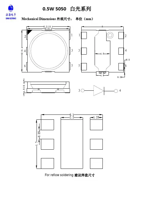
5050贴片详细中文资料数值:5050led的封装尺寸:5mm*5mm*1.6mm,亮度可以达到5500-6000MCD(纯白光,暖光的稍微小一点)。
他的工作电压和普通的led一样,只需要3.2-3.4V,电流也是一样20MA。
由于5050贴片led的体积比较小,做工比较精细,所以手工焊接不大方便,但是不是说不能焊接,其焊接温度要控制在250度内,否则会烫坏较贵的5050贴片led由于5050贴片led参数决定了他必定是款受人喜爱的led,所以他常被用在高端民用节能灯,汽车仪表板,led灯带、手机背光及按键,仪器仪表背光及要求小体积LED之产品,LED背光、开关及标志的平面背光,来电显示、闪光灯、汽车、音响、户内显示屏、照明灯具市场!光电特性参数:电流越大,电压越高,温度越高,电流越小,发光角度:125度等,正向使用电流是60mA,反向电压最大不能超过5V,工作温度在-35~+60℃之间最好。
如果不考虑光衰寿命问题,也可在+85度以下工作,功率:0.18W(与市面上号称0.2W的相同功率)5050LED白光应用参数1、电流:43-46mA(这是最理想的驱动电流);最大使用电流不能超过60mA;2、电压2.8-3.6V(要求灯珠的瞬间电压不能超过5V,要不就对LED灯珠有损坏或严重损坏而无法修复);3、环境温度-20℃~+40℃(要求灯具的散热设计做得比较好,LED灯引脚的温度不能超过60度);4、如果电流在14-20mA的时候,每降低1mA电流,其亮度相应降低4%;5、功率在43-46mA的时候为0.12W,在46-53mA的时候为0.15W,在54-60mA的时候为0.18W;6、耗电量低7、使用寿命长在恰当的电流和电压下,LED的使用寿命可达10万小时。
8 、高亮度、低热量比HID或白炽灯更少的热辐射。
9、环保LED是由无毒的材料作成,不像荧光灯含水银会造成污染,同时LED也可以回收再利用。
LED模组概念:LED模组就是把LED(发光二极管)按一定规则排列在一起再封装起来,加上一些防水处理组成的产品。
就是LED模组。
无极5050LED模组是贴片5050模组,不分正负极接线。
LED模组是LED产品中应用比较广的产品,在结构方面和电子方面也存在很大的差异,简单的就是用一个装有LED的线路板和外壳就成了一个LED模组,复杂的就加上一些控制,恒流源和相关的散热处理使LED寿命和发光强度更好。
模组应用:LED模组主要用于展示广告字体(压克力、吸塑)和标识的夜间效果,它以文字或标识为媒介,安装在楼宇顶部或墙面,既能表现标识白天效果,又能利用LED作为发光光源,在夜间表现出另外一种效果,再配以LED照明应用控制系统,对文字或标识进行动态视频控制,在一些娱乐气氛较浓的场所,LED光源模组已经成了企业展示自我形象的最重要的选择之一。
LED模组分类按颜色种类可以分为单色、七彩、全彩单点控制三种,单色就是单种颜色的模组,一般有红色、绿色、黄色、白色等等是比较常用的;七彩LED模组就是由七种不同颜色进行变换的模组产品,它色彩更多,更有变化性;全彩LED模组与七彩相比则更丰富,它可以实现全真的色彩变幻,不仅非常漂亮,而且动感十足,也更能吸引人的眼球。
按单颗LED的功率又可以分为小功率(0.3W以下)、中功率(0.3-0.5W)、大功率(1W及以上)三种,大功率的模组比小功率在亮度上更高,而且使用时间也更长,是以后整个LED 照明的发展趋势,更具备实用性。
按密封性又可以分为防水和不防水两种。
防水和不防水的模组主要是看应用环境来区分的,一般防水的LED模组可以运用于户外照明和宣传使用,它不会因为进水而发生问题,更适合恶劣的环境应用,而不防水模组则主要是室内用的比较多。
当然,防水的模组比不防水的在价格上也要高一些。
按照LED的形状LED模组分为:直插式LED模组,食人鱼LED模组,贴片LED模组。
LED模组参娄1颜色:按颜色种类可以分为单色、七彩、全彩单点控制三种。
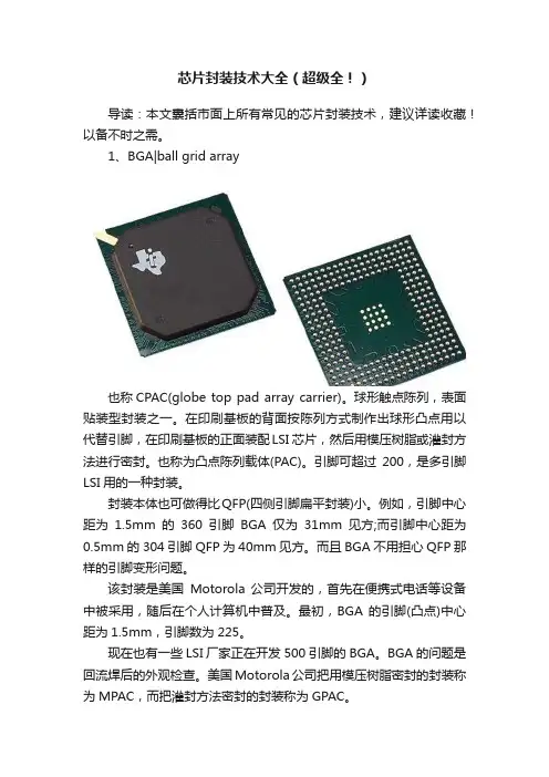
芯片封装技术大全(超级全!)导读:本文囊括市面上所有常见的芯片封装技术,建议详读收藏!以备不时之需。
1、BGA|ball grid array也称CPAC(globe top pad array carrier)。
球形触点陈列,表面贴装型封装之一。
在印刷基板的背面按陈列方式制作出球形凸点用以代替引脚,在印刷基板的正面装配LSI 芯片,然后用模压树脂或灌封方法进行密封。
也称为凸点陈列载体(PAC)。
引脚可超过200,是多引脚LSI用的一种封装。
封装本体也可做得比QFP(四侧引脚扁平封装)小。
例如,引脚中心距为1.5mm的360引脚BGA仅为31mm见方;而引脚中心距为0.5mm的304 引脚QFP 为40mm 见方。
而且BGA不用担心QFP 那样的引脚变形问题。
该封装是美国Motorola 公司开发的,首先在便携式电话等设备中被采用,随后在个人计算机中普及。
最初,BGA 的引脚(凸点)中心距为1.5mm,引脚数为225。
现在也有一些LSI 厂家正在开发500 引脚的BGA。
BGA 的问题是回流焊后的外观检查。
美国Motorola公司把用模压树脂密封的封装称为MPAC,而把灌封方法密封的封装称为GPAC。
2、C-(ceramic)表示陶瓷封装的记号。
例如,CDIP 表示的是陶瓷DIP。
是在实际中经常使用的记号。
3、COB (chip on board)COB (chip on board)板上芯片封装,是裸芯片贴装技术之一,半导体芯片交接贴装在印刷线路板上,芯片与基板的电气连接用引线缝合方法实现,并用树脂覆盖以确保可靠性。
虽然COB 是最简单的裸芯片贴装技术,但它的封装密度远不如TAB和倒片焊技术。
4、DIP(dual in-line package)DIP(dual in-line package) 双列直插式封装。
插装型封装之一,引脚从封装两侧引出,封装材料有塑料和陶瓷两种。
欧洲半导体厂家多用DIL。
Product Data Sheet DS69The Bridgelux SMD 5050 Gen2 high power LED is hot-color targeted, which ensures that the LEDs fall within their specified color bin at the typical application conditions of 85°C. With its broad lumen coverage and wide range of CCT options, the SMD 5050 provides unparalleled design-in flexibility for indoor and outdoor lighting applications. The SMD 5050 is ideal as a drop-in replacement for emitters with an industry standard 5.0mm x 5.0mm footprint.Features• Industry-standard 5050 footprint• 3 bin color control enables tight color control• Hot-color targeting ensures that color is within the ANSI bin at the typical application conditions of 85°C • Enables 3- and 5-step MacAdam ellipse custom binning kits• RoHS compliant and lead free• Multiple CCT configurations for a wide range of lighting applicationsBenefits• Lower operating and manufacturing cost• Ease of design and rapid go-to-market• Uniform consistent white light• Reliable and constant white point• Environmentally friendly, complies with standards • Design flexibilityContentsProduct Feature MapProduct NomenclatureThe part number designation for Bridgelux SMD 5050 is explained as follows:Product Test ConditionsBridgelux SMD 5050 Gen2 LEDs are tested and binned with a 10ms pulse of 125mA at T j (junction temperature)=T sp (solder point temperature) =25°C. Forward voltage and luminous flux are binned at a T j =T sp =25°C, while color is hot targeted at a T sp of 85°C.Bridgelux SMD LED products come in industry standard package sizes and follow ANSI binning standards. These LEDs are optimized for cost and performance, helping to ensure highly competitive system lumen per dollar performance while addressing the stringent efficacy and reliability standards required for modern lighting applications.1 2 3 4 5 6 7 8 9 10 11 12 1314 15 16Product FamilyColor Bin OptionsFlux BinsMinimum CRIC = 70 CRI E = 80 CRI G = 90 CRIForward Voltage Bins Nominal CCT27 = 2,700K 30 = 3,000K 35 = 3,500K 40 = 4,000K 45 = 4,500K 50 = 5,000K 57 = 5,700K 65 = 6,500KBXEP – 30 E – 1 C 5 – 36 B – 00 – 00 – oProduct VersionPower 5 = 4.4W Die count in parallelTypical Forward VoltageDie count in series Yellow phosphor Light Emitting Surface (LES)Cathode MarkProduct Selection GuideThe following product configurations are available:Table 1: S election Guide, Pulsed Measurement Data at 125mA (T j =T sp =25°C)Notes for Table 1:1. The last 7 characters (including hyphens ‘-’) refer to flux bins, forward voltage bins, and color bin options, respectively. “00-00-0” denotes the full distribution of flux, forward voltage, and 7 SDCM color. Example: B XEP-30E-1C5-36B-00-00-0 refers to the full distribution of flux, forward voltage, and color within a 3000K 7-step ANSI standard chromaticity region with a minimum of 80CRI, 1x12 die configuration, 4.4w power, 35.5V typical forward voltage.2. Product CCT is hot targeted at T sp = 85°C. Nominal CCT as defined by ANSI C78.377-2011.3. Listed CRIs are minimum values and include test tolerance.4. Products tested under pulsed condition (10ms pulse width) at nominal drive current where T j =T sp =25°C.5. Bridgelux maintains a ±7.5% tolerance on luminous flux measurements, ±0.1V tolerance on forward voltage measurements, and ±2 tolerance on CRI measurements for the SMD 5050 Gen2.6. Refer to Table 6 and Table 7 for Bridgelux SMD 5050 Gen2 Luminous Flux Binning and Forward Voltage Binning information.Product Selection GuideThe following product configurations are available:Notes for Table 2:1. The last 7 characters (including hyphens ‘-’) refer to flux bins, forward voltage bins, and color bin options, respectively. “00-00-0” denotes the full distribution of flux, forward voltage, and 7 SDCM color. Example: B XEP-30E-1C5-36B-00-00-0 refers to the full distribution of flux, forward voltage, and color within a 3000K 7-step ANSI standard chromaticity region with a minimum of 80CRI, 1x12 die configuration, 4.4w power, 35.5V typical forward voltage.2. Product CCT is hot targeted at T sp = 85°C. Nominal CCT as defined by ANSI C78.377-2011.3. Listed CRIs are minimum values and include test tolerance.4. Bridgelux maintains a ±7.5% tolerance on luminous flux measurements, ±0.1V tolerance on forward voltage measurements, and ±2 tolerance on CRI measurements for the SMD 5050 Gen2.5. Refer to Table 6 and Table 7 for Bridgelux SMD 5050 Gen2 Luminous Flux Binning and Forward Voltage Binning information.6. Typical stabilized DC performance values are provided as reference only and are not a guarantee of performance.7. Typical performance is estimated based on operation under DC (direct current) with LED emitter mounted onto a heat sink with thermal interfacematerial and the solder point temperature maintained at 85°C. Based on Bridgelux test setup, values may vary depending on the thermal design of the luminaire and/or the exposed environment to which the product is subjected.Table 2: Selection Guide, Stabilized DC Performan ce (T sp = 85°C)6,7Table 3:Performance at Commonly Used Drive CurrentsSMD 5050 LEDs are tested to the specifications shown using the nominal drive currents in Table 1. SMD 5050 may also be driven at other drive currents dependent on specific application design requirements. The performance at any drive current can be derived from the current vs. voltage characteristics shown in Figure 2 and the relative luminous flux vs. current characteristics shown in Figure 3. The performance at commonly used drive currents is summarized in Table 3.Notes for Table 3:1. Alternate drive currents in Table 3 are provided for reference only and are not a guarantee of performance.2. Bridgelux maintains a ± 7.5% tolerance on flux measurements.3. Typical stabilized DC performance values are provided as reference only and are not a guarantee of performance.Table 3:Performance at Commonly Used Drive CurrentsSMD 5050 LEDs are tested to the specifications shown using the nominal drive currents in Table 1. SMD 5050 may also be driven at other drive currents dependent on specific application design requirements. The performance at any drive current can be derived from the current vs. voltage characteristics shown in Figure 2 and the relative luminous flux vs. current characteristics shown in Figure 3. The performance at commonly used drive currents is summarized in Table 3.Notes for Table 3:1. Alternate drive currents in Table 3 are provided for reference only and are not a guarantee of performance.2. Bridgelux maintains a ± 7.5% tolerance on flux measurements.3. Typical stabilized DC performance values are provided as reference only and are not a guarantee of performance.Table 3:Performance at Commonly Used Drive Currents(Continued)Notes for Table 3:1. Alternate drive currents in Table 3 are provided for reference only and are not a guarantee of performance.2. Bridgelux maintains a ± 7.5% tolerance on flux measurements.3. Typical stabilized DC performance values are provided as reference only and are not a guarantee of performance.Table 3:Performance at Commonly Used Drive Currents (Continued)Notes for Table 3:1. Alternate drive currents in Table 3 are provided for reference only and are not a guarantee of performance.2. Bridgelux maintains a ± 7.5% tolerance on flux measurements.3. Typical stabilized DC performance values are provided as reference only and are not a guarantee of performance.Electrical CharacteristicsNotes for Table 4:1. The last 7 characters (including hyphens ‘-’) refer to flux bins, forward voltage bins, and color bin options, respectively. “00-00-0” denotes the full distribution of flux, forward voltage, and 7 SDCM color. Example: B XEP-30E-1C5-36B-00-00-0 refers to the full distribution of flux, forward voltage, and color within a 3000K 7-step ANSI standard chromaticity region with a minimum of 80CRI, 1x12 die configuration, 4.4w power, 35.5V typical forward voltage.2. Bridgelux maintains a tolerance of ± 0.1V on forward voltage measurements. Voltage minimum and maximum values at the nominal drive current are guaranteed by 100% test.3. Products tested under pulsed condition (10ms pulse width) at nominal drive current where T sp = 25°C.4. Thermal resistance value was calculated using total electrical input power; optical power was not subtracted from input power.Table 4: Electrical CharacteristicsAbsolute Maximum RatingsTable 5: Maximum RatingsNotes for Table 5:1. The condition of the maximum drive current is limited, Figure 7 can be reference.2. Bridgelux recommends a maximum duty cycle of 10% and pulse width of 10 ms when operating LED SMD at maximum peak pulsed current specified.Maximum peak pulsed current indicate values where LED SMD can be driven without catastrophic failures.3. The maximum drive current for LM80 test result is based on 128% nominal drive current listed.Table 6: Luminous Flux Bin Definitions at 125mA, T sp=25°CTable 6 lists the standard photometric luminous flux bins for Bridgelux SMD 5050 LEDs. Although several bins are listed, product availability in a particular bin varies by production run and by product performance. Not all bins are available in all CCTs.Table 7: Forward Voltage Bin Definition at 125mA, T sp=25°CNote for Table 7:1. Bridgelux maintains a tolerance of ± 0.1V on forward voltage measurements.Note for Table 6:1. Bridgelux maintains a tolerance of ± 7.5% on luminous flux measurements.Table 8: 3- and 5-step MacAdam Ellipse Color Bin DefinitionsNotes for Table 8:1. Color binning at T sp =85°C2.Bridgelux maintains a tolerance of ± 0.007 on x and y color coordinates in the CIE 1931 color space.Figure 1: C.I.E. 1931 Chromaticity Diagram (3 Color Bin Structure, hot-color targeted at T=85°C)spNote for Figure 3:1. Bridgelux does not recommend driving high power LEDs at low currents. Doing so may produce unpredictable results. Pulse width modulation (PWM) is recommended for dimming effects.Figure 2: Drive Current vs. Voltage (T sp =25°C)Figure 3: Typical Relative Luminous Flux vs. Drive Current (T sp =25°C)Figure 4: Typical Relative DC Flux vs. Solder Point TemperatureFigure 5: Typical DC ccx Shift vs. Solder Point TemperatureNotes for Figures 4 & 5:1. Characteristics shown for warm white based on 2700K and 80 CRI.2. Characteristics shown for neutral white based on 4000K and 80 CRI.3. Characteristics shown for cool white based on 5700K and 80 CRI.4. For other color SKUs, the shift in color will vary. Please contact your Bridgelux Sales Representative for more information.Figure 6: Typical DC ccy Shift vs. Solder Point TemperatureNotes for Figure 6:1. Characteristics shown for warm white based on 2700K and 80 CRI.2. Characteristics shown for neutral white based on 4000K and 80 CRI.3. Characteristics shown for cool white based on 5700K and 80 CRI.4. For other color SKUs, the shift in color will vary. Please contact your Bridgelux Sales Representative for more information. Figure 7: Drive Current Derating CurveTypical Radiation PatternFigure 8: Typical Spatial Radiation Pattern at 125mA, T sp =25°CFigure 9: Typical Polar Radiation Pattern at 125mA, T sp =25°CNotes for Figure 8:1. Typical viewing angle is 116⁰.2.The viewing angle is defined as the off axis angle from the centerline where luminous intensity (Iv) is ½ of the peak value.Typical Color Spectrum Figure 10: Typical Color SpectrumNotes for Figure 10:= 25°C1. Color spectra measured at nominal current for Tsp2. Color spectra shown for warm white is 2700K and 80 CRI.3. Color spectra shown for neutral white is 4000K and 80 CRI.4. Color spectra shown for cool white is 5700K and 80 CRI.Mechanical DimensionsFigure 11: Drawing for SMD 5050Notes for Figure 11:1. Drawings are not to scale.2. Drawing dimensions are in millimeters.3. Unless otherwise specified, tolerances are ± 0.10mm.Recommended PCB Soldering Pad PatternReliabilityTable 9: Reliability Test Items and ConditionsNotes for Table 9:1. Measurements are performed after allowing the LEDs to return to room temperature2. T sld : reflow soldering temperature; T a: ambient temperaturePassing CriteriaFigure 12 :Reflow ProfileReflowing CharacteristicsFigure 13 : Pick and PlaceNote for Figure 13:1. When using a pick and place machine, choose a nozzle that has a larger diameter than the LED’s emitting surface. Using a Pick-and-Place nozzle witha smaller diameter than the size of the LEDs emitting surface will cause damage and may also cause the LED to not illuminate.Is greater than LEDsemitting surfaceFigure 14: Emitter Reel DrawingsNote for Figure 14:1. Drawings are not to scale. Drawing dimensions are in millimeters. Figure 15: Emitter Tape DrawingsNote for Figure 15:1. Drawings are not to scale. Drawing dimensions are in millimeters.Figure 16: Emitter Reel Packaging DrawingsNote for Figure 16:1. Drawings are not to scale.Design ResourcesDisclaimersPrecautionsPlease contact your Bridgelux sales representative for assistance.MINOR PRODUCT CHANGE POLICYThe rigorous qualification testing on products offered by Bridgelux provides performance assurance. Slight cosmetic changes that do not affect form, fit, or function may occur as Bridgelux continues product optimization.CAUTION: CHEMICAL EXPOSURE HAZARDExposure to some chemicals commonly used in luminaire manufacturing and assembly can cause damage to the LED emitter. Please consult Bridgelux Application Note AN51 for additional information.CAUTION: EYE SAFETYThis SMD package emits visible light, that, under certain circumstances, could be harmful to the eye. Proper safe -guards must be used.CAUTION: RISK OF BURNDo not touch the SMD LED emitter during operation. Allow the emitter to cool for a sufficient period of time before handling. The SMD LED emitter may reachelevated temperatures such that could burn skin when touched.CAUTIONCONTACT WITH LIGHT EMITTING SURFACE (LES) Avoid any contact with the LES. Do not touch the LES of the emitter or apply stress to the LES (yellow phosphor resin area). Contact may cause damage to the emitterOptics and reflectors must not be mounted in contact with the LES (yellow phosphor resin area).STANDARD TEST CONDITIONSUnless otherwise stated, LED emitter testing is performed at the nominal drive current.About Bridgelux: We Build Light That Transforms© 2018 Bridgelux, Inc. All rights reserved 2018. Product specifications are subject to change without notice. Bridgelux and the Bridgelux stylized logo design are registered trademarks of Bridgelux, Inc. All other trademarks are the property of their respective owners.46430 Fremont Boulevard Fremont, CA 94538Tel (925) At Bridgelux, we help companies, industries and people experience the power and possibility of light. Since 2002, we’ve designed LED solutions that are high performing, energy efficient, cost effective and easy to integrate. Our focus is on light’s impact on human behavior, delivering products that create better environments, experiences and returns—both experiential and financial. And our patented technology drives new platforms for commercial and industrial luminaires.For more information about the company, please visit /Bridgelux /Bridgelux/user/Bridgelux WeChat ID: BridgeluxInChina。
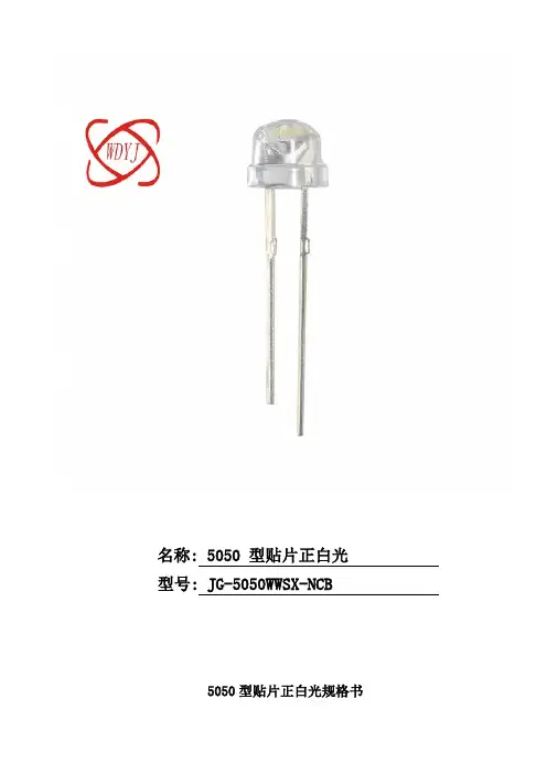
深圳市沃德一佳科技有限公司产品规格书名称: 5050 型贴片正白光型号: JG-5050WWSX-NCB5050型贴片正白光规格书产品应用■ 室内照明:日光灯管、灯条 ■ 商业照明显示:广告字、广告灯箱 ■ LCD 背光源 ■ 装饰照明:柔性灯条 ■ 汽车内部辅助照明 ■ 其它照明和显示类型号材料指南:外形尺寸:附注:1. 所有的尺寸单位为毫米;2. 除特殊要求指出外,公差为± 0.25;3. LED灯是主要是由芯片和环氧树脂组成;4.使用本产品时,注意使用的额定工作条件,未按有关指示操作不当,我司不承担责任;5.此产品注意静电保护光学特性曲线测试电路2.01.5 ity@2mANormalized@25°C0.5操作警惕1.超大电流防范顾客必须应用电阻器保护,否则轻微的电压变化将导致电流大改变(引发爆炸) 2.贮藏2.1产品的存储条件如下:湿度:60% R.H Max.温度:5℃~30℃(41℉~86℉)2.2 密封袋保质期:开包后1个月在<5℃~30℃和<30% R.H.产品必须在一周内使用,或拉链密封≦20R.H的条件下存储.3. 烘烤建议当包装拆封24小时后在软焊前烘烤. 其条件如下:3.1 70±5℃ x(12~24hrs)和<5%RH 卷轴类型3.2 120±5℃ x(1hr~2hr), 散装类型3.3 150±5℃ x(30min~1hr)散装类型。
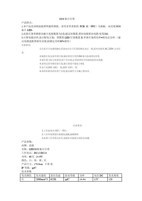
5050贴片灯带产品特点:1.本产品是深圳晶能照明最热销款,采用非常柔软的PCB 板(FPC)为基板,高亮度5050贴片LED,2.此款灯条单路驱动最大连接数量为2卷,超过该数量,要加电源驱动电路.每卷5M。
3.计算电源功率,设计配电方案:预算的LED灯条数量X单条灯条的功率=耗电总功率.(建议电源选配要留有余量,按额定功率80%使用)安装事项:1.注意开关电源的输出直流电压应与灯条的额定电压一致,请勿直接用AC 220V点亮灯条.2.确保灯条安装牢固可靠,最好使用专用的3M强力胶或固定胶垫3.请在剪刀标示处剪切,如户外安装,必须处理好中间接线处防水措施.4.请勿过度弯曲拉扯灯条,最小角度不能低于6度.5.本产品24V为6灯一剪,12V为3灯一剪.6.须在防静电的环境下安装,建议操作人员戴上静电环.注意事项:1.工作温度为-50℃~70℃;2.工作环境周围尽量避免强酸,强碱物体.3.如果工作环境为室外,请做好对接接头的防水问题.产品参数:品牌:晶能名称:LED5050贴片灯带工作电压:DC12/DC24功率:60灯14.4W颜色:白、绿、黄、红产品尺寸:1*0.8cm 5米/卷IP等级:ip67技术参数发光颜色发光强度波长色温防水等级功率电压DC 发光角度红2000mcd*3625K ip67 14.4w 12V 12000led黄2000mcd*300led590K ip67 14.4W 12V 120绿3000mcd*300led5300K ip67 14.4W 12V 120白4500mcd*300led 6000-7000Kip67 14.4W 12V 120暖白4500mcd*300led 2800-3200Kip67 14.4W 12V 120晶能产品特点:1.采用进口高亮芯片、稳定、流明度高2.防护等级高IP673.安装简单方便4.5.应用广6.可随意弯曲。
5050灯珠,5050灯珠参数,...5050灯珠,5050灯珠参数,5050灯珠电压电流,5050灯珠是多少瓦,5050灯珠规格书有哪些?5050灯珠因为体积大,散热性能比较好,所以,很多LED灯珠应用上设计师们都会选择5050灯珠来做光源,特别是5050单色,双色,三色、四色和五色灯珠都能做。
所以,5050灯珠被广泛用在灯带,汽车仪表灯,手机背光及按键,户外照明等产品应用上。
虽然5050灯珠系列应用极广,但是很多工程师和采购朋友在选型和购买的时候,依然对5050灯珠参数,功率,电流,电压不太了解。
常常咨询:5050灯珠是多少瓦?5050灯珠和2835的区别?5050灯珠接线图,5050灯珠参数电压,5050灯珠引脚图,5050灯珠焊盘尺寸,5050灯珠电压电流0.5W,5050灯珠黄光工作电压电流,晶元5050灯珠价格,5050灯珠电压电流0.5W。
像这些5050灯珠的参数问题,一般在5050灯珠规格书里面就有详细的说明了。
5050led贴片灯珠参数1、尺寸:5mm*5mm*1.6mm2、电压:5050白光 3.0-3.4V,3、电流:60mA4、功率:0.2W和0.5W更多的5050灯珠参数请看下图:5050灯珠和3030灯珠有什么区别?1、封装尺寸不同:(1)、5050灯珠封装尺寸是长、宽、高为 5.0X5.0X1.6mm。
(2)、3030灯珠封装尺寸是长、宽、高为 3.0X3.0X0.6mm。
2、颜色不同:(1)、3030灯珠一般主要是做单色灯为主。
(特别以白光1W为主)(2)、5050灯珠常做成双、三色全彩,一灯双色、三色用混合效果好。
3、功率不同:(1)、3030灯珠功率为0.2-1W。
(2)、5050灯珠功率为常规是0.2W-0.5W。
以上是5050灯珠,5050灯珠参数,5050灯珠电压电流,5050灯珠是多少瓦,5050灯珠规格书有哪些的常用参数。
5050灯珠,5050灯珠参数,5050灯珠电压电流,5050灯珠是多少瓦,5050灯珠规格书尺寸都是比较多咨询的。
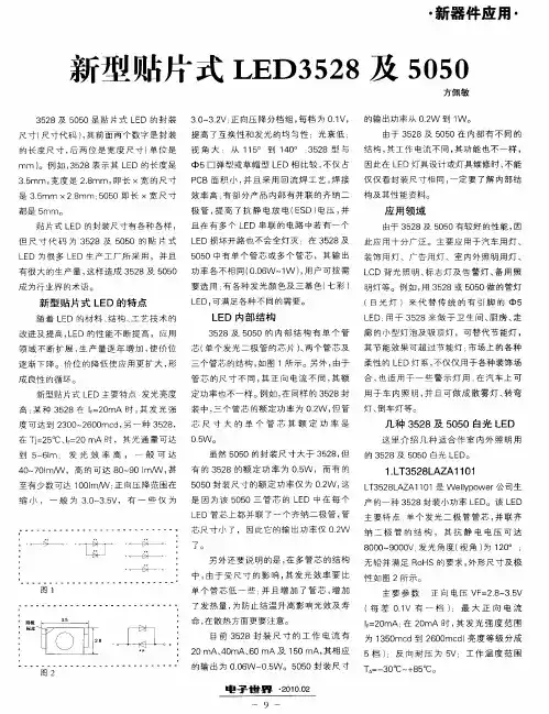
35285050LED 贴片分析及其测试技术基本知识点详
解
正激变换器中同步整流驱动分析透析:Boost 型功率因数校正器的电磁兼容能效标准“吹东风”LED 电视加速普及科学家造全球最小纳米线锂电池微电池有颗纳米芯充电时间更短性能更出色UPS 后备蓄电池容量计算方法介绍中国纯电动客车核心技术已达世界一流水平中科英华新科研成果应用到动力锂电池领域
5050LED 贴片led 封装和3528 贴片led 封装详解
1、3528 贴片led 与5050 贴片有什幺区别
主要是代表规格外形尺寸的表示:35mm*28mm,50mm*50mm 尺寸不一样,功率也不一样,在贴片的应用上,3528 不管是在亮度上还是在寿命上都没有5050 有优势,大小不同样。
2、3528 和5050 贴片LED 有什幺用途?
3528,5050,都是SMD 表贴式LED 封装形式的成品灯尺寸。
用尺寸做名字。
表贴式SMD 灯和直插式DIP 灯相比,亮度偏低,但维修方便,视角也大些。
所以一般室内LED 显示屏用的几乎都是SMD 贴片LED.。
深圳市永而佳电子有限公司LED基本知识培训资料1)LED: Light Emitting Diode 发光二极管LED封装方式封装方式: 1、引脚式(Lamp)LED封装, 2、表面组装(贴片)式(SMT-LED)封装, 3、板上芯片直装式(COB)LED封装, 4、系统封装式(SiP)LED封装 5. 晶片键合和芯片键合.LED分类方法1.按发光管发光颜色分按发光管发光颜色分,可分成红色、橙色、绿色(又细分黄绿、标准绿和纯绿)、蓝光等.另外,有的发光二极管中包含二种或三种颜色的芯片.根据发光二极管出光处掺或不掺散射剂、有色还是无色,上述各种颜色的发光二极管还可分成有色透明、无色透明、有色散射和无色散射四种类型。
散射型发光二极管做指示灯用.2.按发光管出光面特征分按发光管出光面特征分圆灯、方灯、矩形、面发光管、侧向管、表面安装用微型管等。
圆形灯按直径分为φ2mm、φ4.4mm、φ5mm、φ8mm、φ10mm及φ20mm等.国外通常把φ3mm的发光二极管记作T-1;把φ5mm的记作T-1(3/4);把φ4.4mm的记作T-1(1/4).由半值角大小可以估计圆形发光强度角分布情况.从发光强度角分布图来分有三类:(1)高指向性.一般为尖头环氧封装,或是带金属反射腔封装,且不加散射剂。
半值角为5°~20°或更小,具有很高的指向性,可作局部照明光源用,或与光检出器联用以组成自动检测系统.(2)标准型.通常作指示灯用,其半值角为20°~45°.(3)散射型.这是视角较大的指示灯,半值角为45°~90°或更大,散射剂的量较大.3.按发光二极管的结构分按发光二极管的结构分有全环氧包封、金属底座环氧封装、陶瓷底座环氧封装及玻璃封装等结构. 4.按发光强度和工作电流分按发光强度和工作电流分有普通亮度的LED(发光强度<10mcd);超高亮度的LED(发光强度>100mcd);把发光强度在10~100mcd间的叫高亮度发光二极管.一般LED的工作电流在十几mA至几十mA,而低电流LED的工作电流在2mA以下(亮度与普通发光管相同).除上述分类方法外,还有按芯片材料分类及按功能分类的方法.工作电压:一般只有白光,翠绿光和兰光的工作电压在3V以上,其它颜色的工作电压一般在1.8V-2.0V2)波长: 是指不同颜色LED发光的光波的波长,单位nm(纳米),比如各种颜色的波长分别如下:可见光红光:630nm以上纯绿光:520-530黄绿光:530-590黄光:590-600橙光:610-630蓝光:460-490不可见光:850以上为红外光390以下为紫色光上面列举的是一定的发光效率里的波长范围,总之有一个规则:棕红橙黄绿蓝紫:波长越来越短。
[转]5050贴片详细介绍一、5050 贴片详细介绍贴片5050主要应用在灯条灯带,模组,LED显示屏,日光灯,广告背光等,发光角度:120度,耐高温,可用270度回流焊焊接,光通量可达18LM,显示指数可达70%,色温可做到2000-20000K,低光衰3%1千小时/20MA,光色一致性好,无色差。
厚度有两种,1.6MM和2.8MM,硅胶封胶,红光用光磊或晶元芯片,蓝绿用晶元或仕兰芯片,白光用奇力或晶元芯片,芯片规格齐全,有9MIL,12MIL,12*13MIL,14MIL,15MIL,10*23MIL等。
二、3528\5050贴片比较5050贴片led封装和3528贴片led封装详解1、3528 贴片led与5050贴片有什么区别主要是代表规格外形尺寸的表示:35mm*28mm,50mm*50mm 尺寸不一样,功率也不一样,在贴片的应用上,3528不管是在亮度上还是在寿命上都没有5050有优势,大小不同样。
2、3528和5050贴片LED有什么用途?3528,5050,都是SMD表贴式LED封装形式的成品灯尺寸。
用尺寸做名字。
表贴式SMD灯和直插式DIP灯相比,亮度偏低,但维修方便,视角也大些。
所以一般室内LED显示屏用的几乎都是SMD贴片LED。
3 、LED软灯条50505050是LED封装的型号。
以尺寸规格命名。
是指5050型号LED 灯珠。
4、3528和5050贴片LED有什么用途?3528,5050,都是SMD表贴式LED封装形式的成品灯尺寸。
用尺寸做名字。
表贴式SMD灯和直插式DIP灯相比,亮度偏低,但维修方便,视角也大些。
所以一般室内LED显示屏用的几乎都是SMD贴片LED。
5、兼容食人鱼02.03.04怎么意思?SMD是怎么?大功率又是怎么食人鱼是由SMD芯片组成,02.03.04是LED支架的型号。
Surface Mounted Devices的缩写,意为:表面贴装器件SMD 是产品的统一型号。
5050贴片技术大全
:一、5050 贴片详细介绍
贴片5050主要应用在灯条灯带,模组,LED显示屏,日光灯,广告背光等,发光角度:120度,耐高温,可用270度回流焊焊接,光通量可达18LM,显示指数可达70%,色温可做到2000-20000K,低光衰3%1千小时/20MA,光色一致性好,无色差。
厚度有两种,
齐全,有9MIL,12MIL,12*13MIL,14MIL,15MIL,10*23MIL等,交期灵活,欢迎来厂参观。
二、3528\5050贴片比较
5050贴片led封装和3528贴片led封装详解
1、3528 贴片led与5050贴片有什么区别
主要是代表规格外形尺寸的表示:35mm*28mm,50mm*50mm 尺寸不一样,功率也不一样,在贴片的应用上,3528不管是在亮度上还是在寿命上都没有5050有优势,大小不同样。
2、3528和5050贴片LED有什么用途?
:它是Surface Mounted Devices的缩写,意为:表面贴装器件,它是SMT(Surface Mount Technology 中文:表面黏著技术)元器件中的一种。
)表贴式LED封装形式的成品灯尺寸。
用尺寸做名字。
表贴式SMD灯和直插式DIP灯相比,亮度偏低,但维修方便,视角也大
3 、LED软灯条5050
5050是LED封装的型号。
以尺寸规格命名。
是指5050型号LED灯珠。
4、3528和5050贴片LED有什么用途?
3528,5050,都是SMD表贴式LED封装形式的成品灯尺寸。
用尺寸做名字。
表贴式SMD灯和直插式DIP灯相比,亮度偏低,但维修方便,视角也大些。
所以一般室内LED显示屏用的几乎都是SMD贴片LED。
5、兼容食人鱼02.03.04怎么意思?SMD是怎么?大功率又是怎么食人鱼是由SMD芯片组成,02.03.04是LED支架的型号。
Surface Mounted Devices的缩写,意为:表面贴装器件SMD是产品的统一型号。
例如:TOP,Chip,都可以成为SMD,也就是属于平面封装。
SMD芯片有点笼统,用封装5050 或者3528贴片的芯片来做食人鱼。
当然芯片大小又有很多种。
常用来做SMD的尺寸从7×9mil--24×10mil 不等。
大功率是:电压超过0.5W就可以叫大功率了。
LED测试技术的基本知识
【正向电压】通过发光二极管的正向电流为确定值时,在两极间产生的电压降。
【反向电流】加在发光二极管两端的反向电压为确定值时,流过发光二极管的电流。
【峰值波长】光谱辐射功率最大的波长。
【半强度角】在发光(或辐射)强度分布中,发光(或辐射)发光强度大于等于最大强度一半构成的角度。
【主波长】任何一个颜色都可以看作为用某一个光谱色按一定比例与一个
参照光源(如CIE标准光源A、 B、C等,等能光源E,标准照明体D65 等)相混合而匹配出来的颜色,这个光谱色就是颜色的主波长。
颜色的主波长相当于人眼观测到的颜色的色调(心理量)。
若已获得被测LED器件的色度坐标,就可以采用等能白光E光源( x0=0.3333,y0 =0.3333)作为参照光源来计算决定颜色的主波长。
计算时根据色度图上连接参照光源色度点与样品颜色色度点的直线的斜率,查表读出直线与光谱轨迹的交点,确定主波长。
【平均强度】光源在给定方向上的一个很小的立体角元内所包含的光通量d Φv与这个立体角dΩ的比值单位为坎德拉( cd)
【辐射带宽】光谱辐射功率大于等于最大值一半的波长间隔。
三、5050贴片led焊接
我本人对焊接不是太了解,知识会简单的焊接而已,在led节能灯制作过程中我也感觉到5050贴片led焊接是相当的费时的!经过几次实践,我总结了如下几点5050贴片led焊接注意事项:
1、使用功率较小的烙铁(电烙铁的使用方法),我使用的是40W的,建议大家用更小的,推荐使用尖头烙铁,因为贴片的引脚比较细小
2、在5050贴片焊接开始前,我们一定要清理好烙铁的头,防止烙铁头不上锡,如果遇到了烙铁头不上锡,大家可以如是操作:先把烙铁头磨出铜来,在加热的过程中一直泡在松香里,等松香一化就上焊锡丝只到把焊锡融了慢慢涂抹的烙铁头上就行了,如果每次都是一加上都上不了锡那称早换个烙铁头
我在这里强掉要清理烙铁头的原因是为了让烙铁更好的上锡,这样我们就可以挑锡,然后焊接贴片的引脚
3、注意焊接时间,想把主板上锡,然后将5050贴片led放到上过锡的主板上,然后用烙铁头挑锡,放到5050贴片led的引脚上,将其焊接!
我一般都是按照上面的操作的,可能有些词不达意,请各位谅解!
四、单芯贴片5050与三芯贴片5050的差异
1、单芯5050贴片led是最新研究成果的实际应用产品
2、它是三芯产品的升级替代产品,解决了三芯产品本身很多固有的问题
3、它解决了三芯产品的色偏问题,三芯产品有色偏的原因是由于热胀冷缩后导致的荧光粉偏离芯片的圆心,导致蓝光泄露,出现色温不均匀,色斑偏移。
4、它解决了三芯产品元器件多,焊接脚多而导致的元器件故障率高
5、它解决了三芯产品光衰高的问题,原因是三芯都是采用的小功率芯片进行的封装,高档的产品都是采用10mil*18mil的芯片来做,中档的采用9mil的芯片来做。
随着芯片尺寸的加大,光衰趋向于0,这也是为什么路灯采用大功率芯片的原因。
实际上是牺牲了流明光效,减少了光衰,延长了寿命
6、它解决了可靠性问题,这是路灯采用大功率芯片最重要的一个因素。
小功率的灯死灯概率很高。
7、我们的单芯采用的是大尺寸芯片,面积是中档芯片面积的7倍,极大的提高了可靠性
8、我们的单芯产品热阻远低于三芯产品,这对产品的寿命,散热,光效都是非常有贡献的。
9、我公司采用单芯5050生产的led日光灯,经过4个多月24小时的连续运行,未出现光衰问题,具体检测数据见复印件 10 我公司生产的led日光灯整灯包换3年。
这是目前唯一一家承诺三年包换的厂家。
11 达到同等的光衰的流明性价比,我们的最高,市场上还未见如此低光衰产品 12 我们单芯5050在60毫安时流明数为20流明左右 13 单芯显色指数,80以上,普通三芯显色指数不稳定,随温度变化较大总之,单芯的产品达到并超越三芯的高端产品的品质,具有较高的性价比和稳定性,是以后市场的主导方向,目前主要针对高端客户。