DDS正弦信号发生器设计外文文献
- 格式:doc
- 大小:487.50 KB
- 文档页数:15
基于DDS技术的全数控函数发生器【摘要】随着信息技术的发展,现代电子系统对波形发生器提出了更高的要求。
直接数字合成(Direct Digital Synthesize,DDS)是一种重要的频率合成技术,具有分辨率高,频率变换快等优点。
利用键盘输入波形频率,存入单片机,通过单片机控制1602液晶,让1602液晶显示输入频率的大小。
再通过单片机控制AD9851,再经过AD9851内部的相位累加器、相位寄存器、正弦查询表、DAC转换器、内部低通滤波器,然后经外部低通滤波器后,可输出正弦波,或者接到高速比较器上,可输出方波。
【关键词】 DDS;单片机;AD9851【Abstract】 Along with the information technology development, the modern electron system set a higher request to the profile generator.The direct digital synthesis (Direct Digital Synthesize, DDS) is one kind of important frequency synthesis technology, has the resolution to be high, frequency transformation quick and so on ing the keyboard entry profile frequency, stores the monolithic integrated circuit, controls 1602 liquid crystals through the monolithic integrated circuit, lets 1602 liquid crystal display input frequency the size.Again controls AD9851, AD9851through the monolithic integrated circuit after the phase accumulator, the phase register, the sine questionnaire, the DAC switch, after passes through the low pass filter, may output the sine wave, then receives on the high speed comparator, then may output the square-wave.【Key word】DDS; Entire numerical control; Monolithic integrated circuit; 目录前言 (3)1.方案论证与分析 (3)1.1主机的论证与分析 (3)1.2 DDS芯片的论证与分析 (3)1.3显示模块的论证与分析 (4)2.系统硬件设计 (4)2.1 系统设计 (4)2.2 单元电路设计 (5)2.2.1主机模块设计 (5)2.2.2电源模块设计 (5)2.2.3 DDS信号产生模块设计 (5)2.2.4 AD9851的控制字与控制时序 (7)2.2.5 DDS芯片输出频率 (8)2.2.6实现与PC机控制电路设计 (8)2.2.7键盘模块设计 (9)2.2.8显示模块设计 (10)2.2.9低通滤波器电路设计 (10)2.2.10波形调制设计 (11)3.系统软件设计 (11)3.1 主程序 (11)3.2信号频率数字预置子程序 (12)3.3 键盘扫描子程序 (12)3.4 液晶控制器操作流程 (13)4.系统测试 (13)4.1 测试仪器 (13)4.2 测试数据 (13)5.总结与体会 (14)6.参考文献 (14)附录 (14)附一:作品实物及测试图..................... . (14)附二:整机电路图 (16)附三:PCB图 (18)前言本设计采用DDS系统进行频率的直接数字控制。
DDS信号发生器设计源程序(DDS signal generator design source)Program codePrescaler module1, set number:LIBRARY IEEE;USE IEEE.STD_LOGIC_1164.ALL;USE IEEE.STD_LOGIC_ARITH.ALL;USE IEEE.STD_LOGIC_UNSIGNED.ALL;ENTITY Zhishu ISPORT (M:OUT STD_LOGIC_VECTOR (31, DOWNTO, 0));END ENTITY;ARCHITECTURE, func, OF, Zhishu, ISBEGINM < = "00000101010111100110001110111000";END ARCHITECTURE;Accumulation step control module2, step selection:LIBRARY IEEE;USE IEEE.STD_LOGIC_1164.ALL;USE IEEE.STD_LOGIC_ARITH.ALL;USE IEEE.STD_LOGIC_UNSIGNED.ALL;ENTITY bcxuanze ISPORT (bcxzmaichong:IN STD_LOGIC);Bc:BUFFER STD_LOGIC_VECTOR (19, DOWNTO, 0);END ENTITY;ARCHITECTURE, func, OF, bcxuanze, ISSIGNAL bc1:STD_LOGIC_VECTOR (19, DOWNTO, 0): = "00000000000000000001"";SIGNAL bc2:STD_LOGIC_VECTOR (19, DOWNTO, 0): = "00000000000000001010"";SIGNAL bc3:STD_LOGIC_VECTOR (19, DOWNTO, 0): = "00000000000000110010"";SIGNAL bc4:STD_LOGIC_VECTOR (19, DOWNTO, 0): = "00000000000001100100"";SIGNAL bc5:STD_LOGIC_VECTOR (19, DOWNTO, 0): = "00000000001111101000"";SIGNAL tmp:STD_LOGIC_VECTOR (19, DOWNTO, 0);BEGINPROCESS (bcxzmaichong)BEGINIF, bcxzmaichong'EVENT, AND, bcxzmaichong ='1', THENBC < = bc1;BC1 < = bc2;BC2 < = bc3;BC3 < = bc4;Bc4 < = bc5;Bc5 < = bc;END IF;END PROCESS;END ARCHITECTURE;3, cumulative controlLIBRARY IEEE;USE IEEE.STD_LOGIC_1164.ALL;USE IEEE.STD_LOGIC_ARITH.ALL;USE IEEE.STD_LOGIC_UNSIGNED.ALL;ENTITY kongzhi ISPORT (key:IN STD_LOGIC);Clr:IN STD_LOGIC;M:IN STD_LOGIC_VECTOR (19, DOWNTO, 0);Fout:BUFFER STD_LOGIC_VECTOR (19, DOWNTO, 0); END ENTITY;ARCHITECTURE, func, OF, kongzhi, ISBEGINPROCESS (key, CLR)BEGINIF CLR ='0'THENIF, key'EVENT, AND, key ='1', THEN IF fout > 10000 THENFout < = M;ELSEFout < = fout + M;END IF;END IF;ELSEFout < = "00000000000000000000"; END IF;END PROCESS;END ARCHITECTURE;Display module4 frequency displayLIBRARY IEEE;USE IEEE.STD_LOGIC_1164.ALL;USE IEEE.STD_LOGIC_ARITH.ALL;USE IEEE.STD_LOGIC_UNSIGNED.ALL;ENTITY Xianshi ISPORT (foutin:IN STD_LOGIC_VECTOR (19, DOWNTO, 0); Clk:IN STD_LOGIC;Num1:OUT STD_LOGIC_VECTOR (6, DOWNTO, 0);Num2:OUT STD_LOGIC_VECTOR (6, DOWNTO, 0);Num3:OUT STD_LOGIC_VECTOR (6, DOWNTO, 0);Num4:OUT STD_LOGIC_VECTOR (6, DOWNTO, 0);Num5:OUT STD_LOGIC_VECTOR (6, DOWNTO, 0);END ENTITY;ARCHITECTURE, func, OF, Xianshi, ISSIGNAL dec:INTEGER;BEGINDec CONV_INTEGER (foutin); PROCESS (CLK)BEGIN如果clk'event和时钟=“1”然后病例10当0=>num1 < =“1000000”;当1=>num1 < =“1111001”;当2=>num1 < =“0100100”;当3=>num1 < =“0110000”;当4=>num1 < =“0011001”;当5=>num1 < =“0010010”;当6=>num1 <=“00000 10”;当7=>num1 < =“1111000”;当8=>num1 < =“0000000”;当9=>num1 < =“0010000”;当别人= > num1 < =“1111111”;案例;案例(DEC REM 100)/ 10是当0=>num2 < =“1000000”;当1=>num2 < =“1111001”;当2=>num2 < =“0100100”;当3=>num2 < =“0110000”;当4=>num2 < =“0011001”;当5=>num2 < =“0010010”;当6 = > < =“00000 10”num2;当7=>num2 < =“1111000”;当8=>num2 < =“0000000”;当9=>num2 < =“0010000”;当别人= > num1 < =“1111111”;案例;案例(DEC REM 1000)/ 100是当0=>小键盘数字3 < =“1000000”;当1=>小键盘数字3 < =“1111001”;当2=>小键盘数字3 < =“0100100”;当3=>小键盘数字3 < =“0110000”;当4=>小键盘数字3 < =“0011001”;当5=>小键盘数字3 < =“0010010”;当6 = > < =“00000 10”小键盘数字3;当7=>小键盘数字3 < =“1111000”;当8=>小键盘数字3 < =“0000000”;当9=>小键盘数字3 < =“0010000”;当别人= > num1 < =“1111111”;案例;案例(DEC REM 10000)/ 1000是当0=>NUM4 < =“1000000”;当1=>NUM4 < =“1111001”;当2=>NUM4 < =“0100100”;当3=>NUM4 < =“0110000”;当4=>NUM4 < =“0011001”;当5=>NUM4 < =“0010010”;当6=>NUM4 <=”00000 10”;当7=>NUM4 < =“1111000”;当8=>NUM4 < =“0000000”;当9=>NUM4 < =“0010000”;当别人= > num1 < =“1111111”;案例;十二月10000日是当0=> num5 < =“1000000”;当1=> num5 < =“1111001”;当2=> num5 < =“0100100”;当3=> num5 < =“0110000”;当4=> num5 < =“0011001”;当5=> num5 < =“0010010”;当6=> num5 < =“00000 10”;当7=> num5 < =“1111000”;当8=> num5 < =“0000000”;当9=> num5 < =“0010000”;当别人= > num1 < =“1111111”;案例;最后如果;结束进程;端架构;波形存储模块5、提取高8位图书馆的IEEE;使用ieee.std_logic_1164.all;使用ieee.std_logic_arith.all;使用ieee.std_logic_unsigned.all;实体转换为端口(zh_in:在std_logic_vector(19到0);zh_out:出std_logic_vector(7到0));终端实体;是建筑功能的转换开始过程(zh_in)开始zh_out(7)< = zh_in(19);an _ out (6) < = zh _ in (18)._ out (5)) = zh _ in (17)._ out) (4) = zh _ in (16).an _ out (3) < = zh _ in (15)._.) (2) < = zh _ in (14)._ out) (1) < = zh _ in (13).an _ out (0) < = zh _ in (12).end process;end architecture.6、方波生成library ieee;use ieee.std _ logic _ 1164.all.use ieee.std _ logic _ arith.all.use ieee.std _ logic _ unsigned.all.the entity fangboport (fb _ in std _ logic.in _ fbclk std logic;for all _ out std _ logic _ vector (7 downto 0). end entity.the architecture of fangbo funcbeginprocess for _, fbclk)beginif fbclk'event and fbclk =' 1 '.for i in 0 to 7 loopfor _ out (i) < = fb _.end loop;end if;end process;end architecture.7、四路选通library ieee;use ieee.std _ logic _ 1164.all.use ieee.std _ logic _ arith.all. use ieee.std _ logic _ unsigned.all. the company xuanzeport (xzmaichong: in std _ logic.input1: in std _ logic _ vector (7 downto 0). input2: in std _ logic _ vector (7 downto 0). input3: in std _ logic _ vector (7 downto 0). input4: in std _ logic _ vector (7 downto 0). output: out std _ logic _ vector (7 downto 0). end entity.the architecture of xuanze funcsignal count: integer range 0 to 3).beginprocess (xzmaichong)beginif xzmaichong'event and xzmaichong =' 1 '. count = count + 1.end if;if count = 0 thenoutput = input1.elsif count = 1 then output = input2. elsif count = 2 then output = input3. elseoutput = input4.end if;end process;end architecture.。
基于DDS的信号发生器的设计与开发The Design and Development of Function Generator Based on DDS作者:东南大学机械工程系冯建雨关键词:直接数字频率合成低通滤波器正弦波信号1 引言在频率合成(FS- Frequency Synthesis)领域中,常用的频率合成技术有:(1) 直接频率合成(DS);(2) 锁相环频率合成(PLL);(3) 直接数字频率合成(DDS)。
其中,直接数字频率合成(Direct Digital Frequency Synthesis-DDS)是近年来新的FS技术。
由于DDS具有超高速的频率转换时间,极高的频率分辨率和较低的相位噪声,在频率改变与调频时, DDS器件能够保持相位的连续,因此很容易实现频率、相位和幅度调制,此外还具有可编程控制的突出优点。
因此,直接数字频率合成器得到了越来越广泛的应用,成为当今电子系统及设备中频率源的首选器件。
本文在介绍DDS原理的基础上重点介绍利用DDS技术,采用单片机AT89C51控制AD9850芯片实现多功能函数发生器的设计方案。
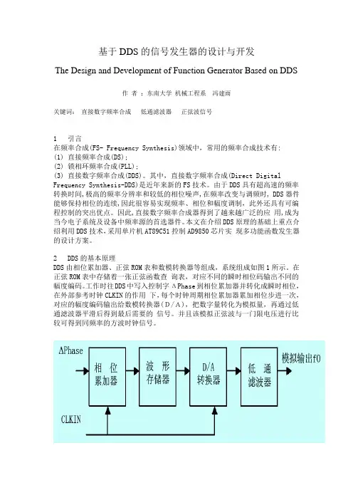
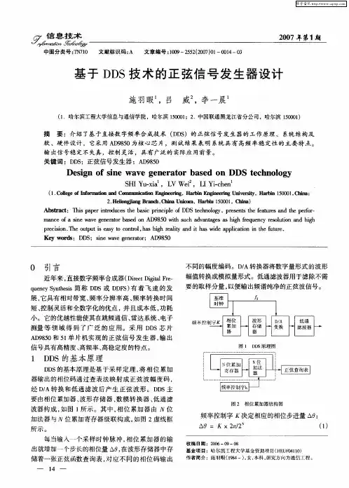
2 DDS的基本原理DDS由相位累加器、正弦ROM表和数模转换器等组成,系统组成如图1所示。
在正弦ROM表中存储着一张正弦函数查询表,对应不同的瞬时相位码输出不同的幅度编码。
工作时往DDS中写入控制字ΔPhase到相位累加器并转化成瞬时相位,在外部参考时钟CLKIN的作用下,每个时钟周期相位累加器累加相位步进一次,对应的幅度编码输出给数模转换器(D/A),把数字量转化为模拟量,再通过低通滤波器平滑后得到最后需要的信号。
并且该模拟正弦波与一门限电压进行比较可得到同频率的方波时钟信号。
图1 DDS原理简图DDS输出信号的频率为最小频率分辨率为最小相位分辨率为式中, △phase为频率控制字, sysclk为系统时钟, CLKIN为DDS的输入参考时钟频率,N为频率寄存器的位数, M为相位偏移寄存器的位数。
基于DDS技术的正弦信号发生器的设计摘要:基于直接数字合成原理,采用单片机STC89C52RC为主控芯片、以可编程DDS集成芯片AD9851为核心,设计了一个正弦信号发生器,输出正弦波形幅度稳定可调,频率精度优于0.1Hz,最高输出频率可达70MHz。
关键词:DDS;信号发生器;AD9851引言信号发生器又称信号源或振荡器,它用于产生被测电路所需特定参数的电测试信号,在生产实践和科技领域中有着广泛应用。
传统的信号源一般采用RC振荡电路、LC振荡电路、石英晶体振荡电路或波形发生集成电路来实现,很难在较宽的频带范围内实现高质量、高频率精度和高稳定性波形的输出,且一般频率调节是通过调节电阻、电感、电容等参数来实现,难于实现高精度和数控调节。
利用直接数字合成技术(DDS)设计的波形发生器具有精度高、稳定性好、频率和波形易于控制等优点,因此,DDS技术越来越广泛地得到应用,成为现代频率合成技术的趋势。
本设计采用STC89C52RC单片机为主控芯片、以可编程DDS集成芯片AD9851为核心,设计了一种结构简单、精度较高、便携式的正弦信号发生器。
1 DDS技术简介DDS是一种运用数字技术来实现产生信号的方法,它从相位概念出发直接合成所需波形的一种频率合成技术。
它主要由三个部分组成:相位累加器、相位幅度转换、数模转换器(DAC)。
其工作原理如图1所示。
图1 DDS工作原理一个正弦波,虽然它的幅度不是线性的,但是它的相位却是线性增加的。
DDS正是利用了这一特点来产生正弦信号。
根据DDS的频率控制字的位数N,把360°平均分成了2N等份。
假设系统时钟为Fc,输出频率为Fout。
每次转动一个角度360°/2N,则可以产生一个频率为Fc/2N的正弦波的相位递增量。
那么只要选择恰当的频率控制字M,使得Fout/Fc=M/2N,就可以得到所需要的输出频率Fout,即Fout=Fc×M/2N。
通过相位累加器,得到合成Fout频率所对应的相位信息,然后相位幅度转换器把0°~360°的相位转换成相应相位的幅度值。
DDS devices to produce high-quality waveform: a simple, efficient and flexibleAbstract: Direct digital frequency synthesis (DDS) technology for the generation and regulation of high-quality waveforms, widely used in medical, industrial, instrumentation, communications, defense and many other areas. This article will briefly describe the technology, on its strengths and weaknesses, examine some application examples, and also introduced some new products that contribute to the promotion1.IntroductionA key requirement in many industries is an exact production, easy operation and quick change of different frequencies, different types of waveforms. Whether it is broadband transceiver requires low phase noise and excellent spurious-free dynamic performance of agile frequency source, or for industrial measurement and control system needs a stable frequency excitation, fast, easy and economical to produce adjustable waveform while maintaining phase continuity capabilities are critical to a design standard, which is what the advantages of direct digital frequency synthesis.2.Frequency synthesis taskThe growing congestion of the spectrum, coupled with lower power consumption, quality of never-ending demand for higher measuring equipment, these factors require the use of the new frequency range, requires a better use of existing frequency range. A result, the search for better control, in most cases, by means of frequency synthesizer for frequency generation. These devices use a given frequency, fC of to generate a target frequency (and phase) fOUT the general relationship can be simply expressed as:fOUT = εx× fCAmong them, the scale factor εx, sometimes known as the normalized frequency.The equation is usually gradual approximation of the real number algorithms. When the scale factor is a rational number, two relatively prime numbers (output frequency and reference frequency) than the harmonic. However, in most cases, εx may belong to a broader set of real numbers, the approximation process is within the acceptable range will be truncatedThe frequency synthesizer a practical way to achieve is the direct digital frequency synthesis (of DDFS), usually referred to as direct digital synthesis (DDS). This technique using digital data processing to generate a frequency and phase adjustable output, the output anda fixed frequency reference clock source fC. related. DDS architecture, the reference or the system clock frequency divided by a scale factor to produce the desired frequency, the scale factor is controlled by the binary tuning word programmable.In short, direct digital frequency synthesizer to convert a bunch of clock pulses into an analog waveform, usually a sine wave, triangle wave or square wave. Shown in Figure 1, its main parts: the phase accumulator (to produce the output waveform phase angle data), relative to digital converter, (above the phase data isconverted to the instantaneous output amplitude data), and digital-to-analog converter (DAC) (the magnitude of data into a sampled analog data points)Figure 2-1 DDS function of the system block diagram.For the sine wave output, relative to digital converter is usually a sine lookup table (Figure 2). Phase accumulator unit count N a relative to the frequency of fC, according to the following equation:The number of pulses of the fC:M is the resolution of the tuning word (24-48)N corresponds to the smallest increment of phase change of the phase accumulator output wordFigure2-2 Typical DDS architecture and signal path (with DACs).Changing N will immediately change the output phase and frequency, so the system has its own continuous phase characteristics, which is one of the key attributes of many applications. No loop settling time, which is different from the analog system, such as phase-locked loops (PLLs). DAC is usually a high-performance circuit, designed specifically for the DDS core (phase accumulator and phase amplitude converter). In most cases, the results of the device (usually single-chip) is generally referred to as the pure DDS or the C-DDS.Actual DDS devices are generally multiple registers, in order to achieve a different frequency and phasemodulation scheme. Such as phase register, their storage phase of increase in the output phase of the phase accumulator. In this way, the corresponding delay output sine wave phase in a phase tuning word. This is useful for phase modulation applications for communication systems. The resolution of the adder circuit determines the number of bits of the phase tuning word, therefore, also decided to delay the resolution.Integrated in a single device on the engine of a DDS and a DAC has both advantages and disadvantages, however, whether integrated or not, need a DAC to produce ultra-high purity high-quality analog signal. DAC will convert digital sinusoidal output to an analog sine wave may be single-ended or differential. Some of the key requirements for low phase noise, excellent wideband (WB) and narrowband (NB), spurious-free dynamic range (SFDR), and low power consumption. If the external device, the DAC must be fast enough to handle the signal, so the built-in parallel port device is very common.3.DDS and other solutionsThe frequency analog phase-locked loops (PLLs), clock generator, and the use of FPGA dynamic programming of the output of the DAC. By examining the spectrum of performance and power of these technologies, a simple comparison, Table 1 shows the qualitative results of the comparisonTable 3-1DDS with competing technologies - Advanced comparePower consumption Spectral purity RemarksDDS Low Middle Ease of tuningDiscrete DAC+FPGA Middle Middle-High With tuning capabilitiesAnalog PLL Milddle High Difficult tuningPhase-locked loop is a feedback loop and its components: a phase comparator, a divider and a pressure-controlled oscillator (VCO), phase comparator reference frequency and output frequency (usually the output frequency is N)frequency) were compared. The error voltage generated by the phase comparator is used to adjust the VCO, thus the output frequency. When the loop is established, the output frequency and / or phase with the reference frequency to maintain a precise relationship. PLL has long been considered in a particular frequency range, high fidelity and consistent signal low phase noise and high spurious free dynamic range (SFDR) are ideal for applications.PLL can not be precisely and quickly tuning the frequency output waveform, and the slow response, which limits their applicability for fast frequency hopping and part of the frequency shift keying and phase shift keying applications.Other programs, including integrated DDS engine field programmable gate arrays (FPGAs) - a synthetic sine wave output with the off-the-shelf DAC - though the PLL frequency-hopping problem can be solved, but there own shortcomings. The defects of the major systems work and interface power requirements, high cost, large size, and system developers must also consider the additional software, hardware and memory. For example, using the DDS engine option in the modern FPGA to generate the 10 MHz output signal dynamic range is 60 dB up to 72 kB memory space. In addition, designers need to accept and be familiar with thesubtle balance DDS core architecture. .From a practical point of view (see Table 2), thanks to the rapid development of CMOS technology and modern digital design techniques, as well as the improvement of the DAC topology, DDS technology has been able to achieve unprecedented low power consumption in a wide range of applications, spectrum performance and cost levels. Although the pure DDS products in performance and design flexibility to achieve the level of high-end DAC technology and FPGA, but the advantages of DDS in terms of size, power consumption, cost and simplicity, making it the primary choice for many applications.Table 3-2 Benchmark Analysis Summary - frequency generation technique (<50 MHz)Phase -locked loop DAC + FPGA DDS Spectral performance High High MiddleSystem power requirements High High MiddleDigital frequency tuning No Yes YesTuning response time High Low LowSolution size Middle High LowWaveform flexibility Low Middle HighCost Middle High LowDesign reuse Middle Low HighImplementation complexity Middle High LowAlso be noted that the DDS device for digital methods to produce the output waveform, it can simplify some of the architecture of the solution, or the waveform of digital programming to create the conditions. Usually with a sine wave to explain the functions and working principle of the DDS, but using modern DDS ICs can easily generate a triangle wave or square wave (clock) output, thereby eliminating the former case the lookup table, and the latter case the DAC the need to integrate a simple and accurate enough.4. Performance and limitations of the DDS4.1 Image and envelope: Sin (x) xx roll-offThe actual output of the DAC is not a continuous sine wave, but a series of pulses with a sinusoidal time envelope. The corresponding spectrum is a series of image and signal aliasing. Image along the sin (x) / x envelope distribution (see Figure 3 | margin | graph). The need for the filter to suppress frequencies outside the target band, but can not inhibit the high-level in the passband aliasing (for example, caused due to DAC non-linear)The Nyquist criterion requires that each cycle requires at least two sampling points in order to rebuild the desired output waveform. The Mirroring response arising from sampling the output frequency K, CLOCK ×OUT In this example, which CLOCK = 25 25 MHz and fOUT = 5 MHz, the first and second mirror frequency appear in (see Figure 3) fCLOCK × fOUT, o 20 MHz and 30 MHz. The third and fourth mirror frequency at 45 MHz and 55 MHz. Note, sin (x) / x value of zero at multiples of the sampling frequency.When fOUT greater than the Nyquist bandwidth (1/2 f CLOCK), the first mirror frequency will appear in the Nyquist bandwidth, the occurrence of aliasing (such as 15 MHz signal aliasing down to 10 MHz). Can not use the traditional quist anti-aliasing filter to filter out aliasing mirror frequency from the outputFigure 4-1 Sin, in Figure 3.DDS, (x) / x roll-off.In a typical DDS application, the use of a low-pass filter to suppress the mirror frequency response of the output spectrum. To make the low-pass filter cutoff frequency to remain at reasonable levels, and keep it simple filter design, a feasible approach is the use of an economic low-pass output filter bandwidth limited to about 40% of the frequency of clock.Any given mirror frequency relative to the amplitude of the fundamental formula of sin (x) / x calculation. Because the function of the frequency roll-off, the basic output of the amplitude and the output frequency is inversely proportional to decrease; in the DDS system, reduce the amount of DC-Nyquist bandwidth range of -3.92 dB.Significant reduction in frequency in the first mirror - the fundamental 3 dB range. In order to simplify the DDS application filtering, frequency plan must be formulated and analyzed to mirror the frequency and magnitude of the sin (x) / x response in the OUT and CLOCK target frequency spectrum requirements. Other unwanted frequencies in the output spectrum (such as integral and differential linearity error of the DAC, the surge of energy associated with the DAC and clock feed through noise) does not follow the sin (x) / x roll-off response. These unwanted frequencies will be harmonic and spurious energy in the output spectrum in many places - but its magnitude is generally far below the mirror frequency response. DDS devices to the general background noise, substrate noise, thermal noise effects, ground coupling and other signal source coupling factor cumulative portfolio decisions. DDS devices, the noise floor performance of stray and jitter by the circuit board layout, power quality, and - most importantly - Enter the profound impact of the quality of the reference clock.4.2ShakeThe edge of the perfect clock source will be the precise time interval, the interval will never change. Of course, this is not possible; even the best oscillator is also the ideal components constitute, with noise and other defects. Quality and low phase noise crystal oscillator jitter picosecond, and is built up from one millionthe number of clock edge. The factors leading to jitter external interference, thermal noise, the oscillator circuit instability and power, ground and output connections bring, all these factors will interfere with the timing characteristics of the oscillator. In addition, the oscillator by the external magnetic field or electric field and the nearby transmitter RF interference. Oscillator circuit, a simple amplifier, inverter or buffer to signal additional jitter.Therefore, the choice of a low-jitter, and the edge of steep stable reference clock oscillator is critical. Higher frequency reference clock allows a larger sample, and divide to some extent, reduce the jitter, because the signal to divide a long time to produce the same amount of jitter, which can reduce the jitter on the signal percentage.4.3 Noise - including the phase noiseThe sampling system noise depends on many factors, the most important factor is the reference clock jitter, this jitter performance of phase noise on fundamental signal. In the DDS system, the register output of the truncated phase may bring the system error code. The binary word does not lead to the truncation error. But for non-binary word, phase noise truncation error in the spectrum spurious. Spurious frequency / amplitude depends on the code word. Quantification and linearity error of the DAC will be brought to the system harmonic noise. Time-domain error (such as owed to the red / overshoot and code errors) will increase the output signal distortion.5. Application5.1 DDS applications can be divided into two categories:Require agile frequency source for data coding and modulation applications, communications and radar systemsRequire measurement of the universal frequency synthesizer features and programmable tuning, scanning, and motivational skills, industrial and optical applicationsBoth cases, the trend toward higher spectral purity (low phase noise and higher spurious free dynamic range), also low power and small size requirements to accommodate the remote ordemand for battery-powered devices.5.2 Modulation / data encoding, and synchronization of the DDSDDS products first appeared on the radar and military applications and the development of some of its characteristics (performance improvements, cost and size, etc.) DDS technology is becoming more prevalent in the modulation and data encoding applications. This section will discuss the two data encoding scheme in the DDS system.5.3 Binary frequency shift keyingThe launch of the data is a continuous carrier frequency in two discrete frequency (binary one, ie, pass number, a binary 0, namely, the transformation between the space). Figure 4 shows the relationship between the data and transmit signals.Figure 5-1 binary FSK modulation.Binary 1 and 0 for two different frequencies f0 and f1, respectively. This encoding scheme can be easily DDS device. On behalf of the output frequency of the DDS frequency tuning word change to f0 and f1, will launch the 1 and 0. To transform the output frequency shall dedicated pin FSELECT, containing the appropriate tuning word registers (see Figure 5)Figure 5-2 AD9834 or AD9838 DDS tuning word selector realization of the FSK encoding.5.4 Phase shift keying (PSK)In PSK, the carrier frequency remains the same, by changing the phase of the transmitted signal to transmit information. Can take advantage of a variety of programs to achieve PSK,. The easiest way is often referred to as binary PSK (BPSK), using only two signal phase: 0 ° (logic 1) and 180 ° (logic 0). Members state depends on the status of the former one. If the wave phase remains unchanged, the signal state will remain the same (low or high). Wave phase change 180 °, ie, phase inversion, the signal state will change (low into high or high to low). PSK coding in DDS products can be easily achieved, because most devices have a separate input register (phase register), and phase values can be loaded. This value is added directly to the carrier phase, without changing its frequency. Change the contents of the register will be modulated carrier phase, resulting in a PSK output. For applications that require high-speed modulation, built-in phase register of the AD9834 and AD9838 allow PSELECT pin signal transformation, according to need modulated carrierin the preloaded phase registers.The more complex the PSK four or eight-wave phase. Thus, whenever the phase change of binary data transfer rate will be higher than the BPSK modulation. In the four-phase modulation (Quadrature PSK), in the phase angle of 0 ° to +90 °, -90 ° and +180 °; each phase to transform the two signals may represent a factor AD9830, AD9831, AD9832, and the AD9835 provides four phase registers, can be continuously updated register of different phase shift, the complex phase modulation scheme.5.5 The use of synchronous mode of multiple DDS devices to achieve the I / QMultiple DDS components to achieve the many applications of the I / Q sine wave or square wave signal of known phase relationship between two or more synchronous mode. A common example is the same phase and quadrature modulation (I / Q) in this technique, the phase angle of 0 ° and 90 ° from the carrier frequency signal information. To run two separate DDS components, you can use the same source clock to output can directly control and manipulate the signal of the phase relationship. In Figure 6, with a reference clock on the AD9838 device programming; the RESET pin is used to update the two devices. In this way, you can achieve a simple I / Q modulationRESET after power and initialized before any data to the DDS transmission. DDS output results can be placed in a known phase, making it a common reference point of view, in order to synchronize multiple DDS devices. When new data is sent to multiple DDS devices, the DDS can remain relevant phase relationship, or by the phase offset register can predict the relative phase shift between the adjustments of multiple DDS. The AD983x series of DDS products have a 12 phase resolution, the effective resolution of 0.1 °.Figure 5-3 Synchronize the two DDS components.DDS器件产生高质量波形:简单、高效而灵活摘要:直接数字频率合成(DDS)技术用于产生和调节高质量波形,广泛用于医学、工业、仪器仪表、通信、国防等众多领域。
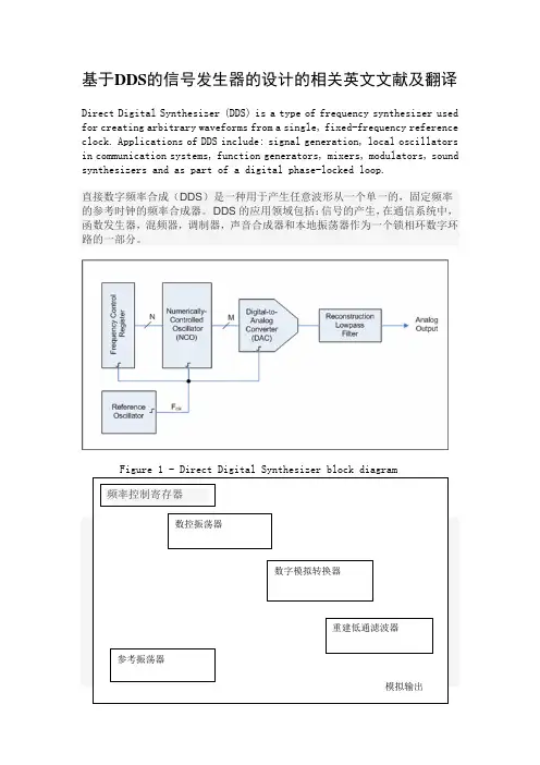
基于DDS的信号发生器的设计的相关英文文献及翻译Direct Digital Synthesizer (DDS) is a type of frequency synthesizer used for creating arbitrary waveforms from a single, fixed-frequency reference clock. Applications of DDS include: signal generation, local oscillators in communication systems, function generators, mixers, modulators,sound synthesizers and as part of a digital phase-locked loop.直接数字频率合成(DDS)是一种用于产生任意波形从一个单一的,固定频率的参考时钟的频率合成器。
DDS的应用领域包括:信号的产生,在通信系统中,函数发生器,混频器,调制器,声音合成器和本地振荡器作为一个锁相环数字环路的一部分。
Figure 1 - Direct Digital Synthesizer block diagram图1 - 直接数字频率合成器框图A basic Direct Digital Synthesizer consists of a frequency reference (often a crystal or SAW oscillator), a numerically controlled oscillator (NCO) and a digital-to-analog converter (DAC) as shown in Figure 1.The reference provides a stable time base for the system and determines the frequency accuracy of the DDS. It provides the clock to the NCO which produces at its output a discrete-time, quantized version of the desired output waveform (often a sinusoid) whose period is controlled by the digital word contained in the Frequency Control Register. The sampled, digital waveform is converted to an analog waveform by the DAC. The output reconstruction filter rejects the spectral replicas produced by the zero-order hold inherent in the analog conversion process.A DDS has many advantages over its analog counterpart, the phase-locked loop (PLL), including much better frequency agility, improved phase noise, and precise control of the output phase across frequency switching transitions. Disadvantages include spurious due mainly to truncation effects in the NCO, crossing spurious resulting from high order (>1) Nyquist (尼奎斯特定理) images, and a higher noise floor at large frequency offsets due mainly to the Digital-to-analog converter.Because a DDS is a sampled system, in addition to the desired waveform at output frequency Fout, Nyquist images are also generated (the primaryimage is at Fclk -Fout, where Fclkis the reference clock frequency). In orderto reject these undesired images, a DDS is generally used in conjunction with an analog reconstruction lowpass filter as shown in Figure 1.The output frequency of a DDS is determined by the value stored in the frequency control register (FCR) (see Fig.1), which in turn controls the NCO's phase accumulator step size. Because the NCO operates in the discrete-time domain, it changes frequency instantaneously at the clock edge coincident with a change in the value stored in the FCR. The DDS output frequency settling time is determined mainly by the phase response of the reconstruction filter. An ideal reconstruction filter with a linear phase response (meaning the output is simply a delayed version of the input signal) would allow instantaneous frequency response at its output because a linear system can not create frequencies not present at its input.The superior close-in phase noise performance of a DDS stems from the fact that it is a feed-forward system. In a traditional phase locked loop (PLL), the frequency divider in the feedback path acts to multiply the phase noise of the reference oscillator and, within the PLL loop bandwidth, impresses this excess noise onto the VCO output. A DDS on the other hand, reduces the reference clock phase noise by the ratio f clk/f out,because its output is derived by fractional division of the clock. Reference clock jitter translates directly to the output, but this jitter is a smaller percentage of the output period (by the ratio above). Since the maximum output frequency is limited to f clk/2, the output phase noise at close-in offsets is always at least 6dB below the reference clock phase-noise.At offsets far removed from the carrier, the phase-noise floor of a DDS is determined by the power sum of the DAC quantization noise floor and the reference clock phase noise floor.一个DDS以上的锁相回路(PLL),其模拟对应,许多优势,包括更好的频率灵活性,提高了相位噪声,整个频率转换开关的输出相位的精确控制。
EDA课程设计——基于DDS的正弦信号发生器设计(模版)第一篇:EDA课程设计——基于DDS的正弦信号发生器设计(模版)顶层文件LIBRARY IEEE;USE IEEE.STD_LOGIC_1164.ALL;USE IEEE.STD_LOGIC_UNSIGNED.ALL;ENTITY DDS ISPORT(K:IN STD_LOGIC_VECTOR(9 DOWNTO 0);EN:IN STD_LOGIC;RESET:IN STD_LOGIC;CLK:IN STD_LOGIC;Q:OUT STD_LOGIC_VECTOR(8 DOWNTO 0));END ENTITY DDS;ARCHITECTURE BEHAVE OF DDS ISCOMPONENT SUM99 ISPORT(K:IN STD_LOGIC_VECTOR(9 DOWNTO 0);EN:IN STD_LOGIC;RESET:IN STD_LOGIC;CLK:IN STD_LOGIC;OUT1:OUT STD_LOGIC_VECTOR(9 DOWNTO 0));END COMPONENT SUM99;COMPONENT REG1 ISPORT(D:IN STD_LOGIC_VECTOR(9 DOWNTO 0);CLK:IN STD_LOGIC;Q:OUT STD_LOGIC_VECTOR(9 DOWNTO 0));END COMPONENT REG1;COMPONENT ROM ISPORT(CLK:IN STD_LOGIC;ADDR:IN STD_LOGIC_VECTOR(9 DOWNTO 0);OUTP:OUT STD_LOGIC_VECTOR(8 DOWNTO 0));END COMPONENT ROM;COMPONENT REG2 ISPORT(D:IN STD_LOGIC_VECTOR(8 DOWNTO 0);CLK:IN STD_LOGIC;Q:OUT STD_LOGIC_VECTOR(8 DOWNTO 0));END COMPONENT REG2;SIGNAL S1:STD_LOGIC_VECTOR(9 DOWNTO 0);SIGNAL S2:STD_LOGIC_VECTOR(9 DOWNTO 0);SIGNAL S3:STD_LOGIC_VECTOR(8 DOWNTO 0);BEGINU0:SUM99PORTMAP(K=>K,EN=>EN,RESET=>RESET,CLK=>CLK,OUT1=>S1);U1:REG1 PORT MAP(D=>S1,CLK=>CLK,Q=>S1);U2:ROM PORT MAP(ADDR=>S2,CLK=>CLK,OUTP=>S3);U3:REG2 PORT MAP(D=>S3,CLK=>CLK,Q=>Q);END ARCHITECTURE BEHAVE;正弦查找表 LIBRARY IEEE;USE IEEE.STD_LOGIC_1164.ALL;USE IEEE.STD_LOGIC_ARITH.ALL;USEIEEE.STD_LOGIC_UNSIGNED.ALL;ENTITY ROM IS PORT(ADDR:IN STD_LOGIC_VECTOR(6 DOWNTO 0);CLK:IN STD_LOGIC;OUTP:OUT SIGNED(7 DOWNTO 0));END ENTITY ROM;ARCHITECTURE ART OF ROM IS BEGIN PROCESS(CLK)IS BEGIN IF(CLK'EVENT AND CLK='1')THEN CASE ADDR IS WHEN “0000000”=>OUTP<=“00000000”;WHEN“0000001”=>OUTP<=“00000010”;WHEN“0000010”=>OUTP<=“00000011”;WHEN“0000011”=>OUTP<=“00000101”;WHEN“0000100”=>OUTP<=“00000110”;WHEN “0000101”=>OUTP<=“00001000”;WHEN “0000110”=>OUTP<=“00001001”;WHEN“0000111”=>OUTP<=“00001011”;WHEN“0001000”=>OUTP<=”00001101“;WHEN ”0001001“=>O UTP<=”00001110“;WHEN ”0001010“=>OUTP<=”0001000 0“;WHEN ”0001011“=>OUTP<=”00010001“;WHEN ”000 1100“=>OUTP<=”00010011“;WHEN ”0001101“=>OUTP< =”00010100“;WHEN ”0001110“=>OUTP<=”00010110“; WHEN ”0001111“=>OUTP<=”00010111“;WHEN ”0010000“=>OUTP<=”00011001“;WHEN ”0010001“=>OUTP<=”0 0011011“;WHEN ”0010010“=>OUTP<=”00011100“;WHEN ”001 0011“=>OUTP<=”00011110“;WHEN ”0010100“=>OUTP< =”00011111“;WHEN ”0010101“=>OUTP<=”00100001“; WHEN ”0010110“=>OUTP<=”00100010“;WHEN ”0010111“=>OUTP<=”00100100“;WHEN ”0011000“=>OUTP<=”0 0100101“;WHEN ”0011001“=>OUTP<=”00100111“;WHEN ”0011010“=>OUTP<=”00101001“;WHEN ”001 1011“=>OUTP<=”00101010“;WHEN ”0011100“=>OUTP< =”00101100“;WHEN ”0011101“=>OUTP<=”00101101“; WHEN ”0011110“=>OUTP<=”00101111“;WHEN ”0011111“=>OUTP<=”00110000“;WHEN ”0100000“=>OUTP<=”0 0110010“;WHEN ”0100001“=>OUTP<=”00110011“;WHEN ”0100010“=>OUTP<=”00110101“;WHEN ”0100011“=>O UTP<=”00110110“;WHEN ”0100100“=>OUTP<=”0011100 0“;WHEN ”0100101“=>OUTP<=”00111001“;WHEN ”010 0110“=>OUTP<=”00111011“;WHEN ”0100111“=>OUTP< =”00111100“;WHEN ”0101000“=>OUTP<=”00111110“; WHEN ”0101001“=>OUTP<=”00111111“;WHEN ”0101010“=>OUTP<=”01000001“;WHEN ”0101011“=>OUTP<=”0 1000011“;WHEN ”0101100“=>OUTP<=”01000100“;WHEN ”0101101“=>OUTP<=”01000110“;WHEN ”0101110“=>O UTP<=”01000111“;WHEN ”0101111“=>OUTP<=”01001001“;WHEN ”0110000“=>OUTP<=”01001010“;WHEN ”011 0001“=>OUTP<=”01001100“;WHEN ”0110010“=>OUTP< =”01001101“;WHEN ”0110011“=>OUTP<=”01001111“; WHEN ”0110100“=>OUTP<=”01010000“;WHEN ”0110101“=>OUTP<=”01010001“;WHEN ”0110110“=>OUTP<=”0 1010011“;WHEN ”0110111“=>OUTP<=”01010100“;WHEN ”0111000“=>OUTP<=”01010110“;WHEN ”0111001“=>O UTP<=”01010111“;WHEN ”0111010“=>OUTP<=”0101100 1“;WHEN ”0111011“=>OUTP<=”01011010“;WHEN ”011 1100“=>OUTP<=”01011100“;WHEN ”0111101“=>OUTP< =”01011101“;WHEN ”0111110“=>OUTP<=”01011111“; WHEN ”0111111“=>OUTP<=”01100000“;WHEN ”1000000“=>OUTP<=”01100010“;WHEN ”1000001“=>OUTP<=”0 1100011“;WHEN ”1000010“=>OUTP<=”01100100“;WHEN ”1000011“=>OUTP<=”01100110“;WHEN ”1000100“=>O UTP<=”01100111“;WHEN ”1000101“=>OUTP<=”0110100 1“;WHEN ”1000110“=>OUTP<=”01101010“;WHEN ”100 0111“=>OUTP<=”01101100“;WHEN ”1001000“=>OUTP< =”01101101“;WHEN ”1001001“=>OUTP<=”01101110“; WHEN ”1001010“=>OUTP<=”01110000“;WHEN ”1001011“=>OUTP<=”01110001“;WHEN ”1001100“=>OUTP<=”0 1110011“;WHEN ”1001101“=>OUTP<=”01110100“;WHEN ”1001110“=>OUTP<=”01110101“;WHEN ”1001111“=>O UTP<=”01110111“;WHEN ”1010000“=>OUTP<=”0111100 0“;WHEN ”1010001“=>OUTP<=”01111010“;WHEN ”101 0010“=>OUTP<=”01111011“;WHEN ”1010011“=>OUTP< =”01111100“;WHEN ”1010100“=>OUTP<=”01111110“; WHEN ”1010101“=>OUTP<=”01111111“;WHEN ”1010110“=>OUTP<=”10000000”;WHEN“1010111”=>OUTP<=“10000010”;WHEN“1011000”=>OUTP<=“10000011”;WHEN“1011001”=>OUTP<=“10000100”;WHEN“1011010”=>OUTP<=“10000110”;WHEN“1011011”=>OUTP<=“10000111”;WHEN “1011100”=>OUTP<=“10001000”;WHEN “1011101”=>OUTP<=“10001010”;WHEN“1011110”=>OUTP<=“10001011”;WHEN“1011111”=>OUTP<=“10001100”;WHEN“1100000”=>OUTP<=“10001110”;WHEN“1100001”=>OUTP<=“10001111”;WHEN“1100010”=>OUTP<=“10010000”;WHEN“1100011”=>OUTP<=“10010010”;WHEN“1100100”=>OUTP<=“10010011”;WHEN“1100101”=>OUTP<=“10010100”;WHEN “00001100110”=>OUTP<=“10010101”;WHEN “1100111”=>OUTP<=“10010111”;WHEN“1101000”=>OUTP<=“10011000”;WHEN“1101001”=>OUTP<=“10011001”;WHEN“1101010”=>OUTP<=“10011010”;WHEN“1101011”=>OUTP<=“10011100”;WHEN“1101100”=>OUTP<=“10011101”;WHEN“1101101”=>OUTP<=“10011110”;WHEN“1101110”=>OUTP<=“10011111”;WHEN“1101111”=>OUTP<=“10100001”;WHEN“1110000”=>OUTP<=“10100010” WHEN “1110001”=>OUTP<=“10100011”;WHEN “1110010”=>OUTP<=“10100100”;WHEN “1110011”=>OUTP<=“10100101”;WHEN“1110100”=>OUTP<=“10100111”;WHEN“1110101”=>OUTP<=“10101000”;WHEN“1110110”=>OUTP<=“10101001”;WHEN“1110111”=>OUTP<=“10101010”;WHEN“1111000”=>OUTP<=“10101011”;WHEN“1111001”=>OUTP<=“10101100”;WHEN“1111010”=>OUTP<=“10101110”;WHEN“1111011”=>OUTP<=“10101111”;WHEN“1111100”=>OUTP<=“10110000”;WHEN“1111101”=>OUTP<=“10110001”;WHEN“1111110”=>OUTP<=“10110010”;WHEN“1111111”=>OUTP<=“10110011”;WHENOTHERS=>OUTP<=“ 00000000”;END CASE;END IF;END PROCESS;END ARCHITECTURE ART;DAC 0832的VHDL程序LIBRARY IEEE;USE IEEE.STD_LOGIC_1164.ALL;USEIEEE.STD_LOGIC_UNSIGNED.ALL;USEIEEE.STD_LOGIC_ARITH.ALL;ENTITY DAC0832 IS PORT(CLK:IN STD_LOGIC;RST:IN STD_LOGIC;ILE:OUT STD_LOGIC;CONT:OUT STD_LOGIC;DATA_OUT:OUT STD_LOGIC_VECTOR(7 DOWNTO 0));END ENTITY;ARCHITECTURE BEHAVE OF DAC0832 IS SIGNAL Q:INTEGER RANGE 0 TO 63;SIGNAL DATA:STD_LOGIC_VECTOR(7 DOWNTO 0);BEGIN PROCESS(CLK)BEGINIF RST='1'THEN Q<=0;ELSIF CLK'EVENT AND CLK='1'THEN IF DATA=“11111111”THEN DATA<=“00000000”;ELSE DATA<=DATA+1;END IF;ELSE Q<=Q+1;END IF;END PROCESS;ILE<='1';CONT<='0';DATA_OUT<=DATA;END ARCHITECTURE BEHAVE;频率控制字 LIBRARY IEEE;USE IEEE.STD_LOGIC_1164.ALL;USE IEEE.STD_LOGIC_UNSIGNED.ALL;ENTITY REG0 ISPORT(CLK:IN STD_LOGIC;LOCK:IN STD_LOGIC;Q:OUT STD_LOGIC_VECTOR(9 DOWNTO 0));END ENTITY REG0;ARCHITECTURE ART OF REG0 IS BEGINPROCESS(CLK)BEGINIF(CLK'EVENT AND CLK='1')THENIF LOCK='1'THENQ<=“0000011111”;END IF;END IF;END PROCESS;END ARCHITECTURE ART;相位寄存器LIBRARY IEEE;USE IEEE.STD_LOGIC_1164.ALL;ENTITY REG1 ISPORT(D:IN STD_LOGIC_VECTOR(9 DOWNTO 0);CLK:IN STD_LOGIC;Q:OUT STD_LOGIC_VECTOR(9 DOWNTO 0));END ENTITY REG1;ARCHITECTURE BEHAVE OF REG1 IS BEGINPROCESS(CLK)ISBEGINIF(CLK'EVENT AND CLK='1')THENQ<=D;END IF;END PROCESS;END ARCHITECTURE BEHAVE;输出数据寄存器LIBRARY IEEE;USE IEEE.STD_LOGIC_1164.ALL;ENTITY REG2 IS PORT(D:IN STD_LOGIC_VECTOR(8 DOWNTO 0);CLK:IN STD_LOGIC;Q:OUT STD_LOGIC_VECTOR(8 DOWNTO 0));END ENTITY REG2;ARCHITECTURE BEHAVE OF REG2 IS BEGINPROCESS(CLK)ISBEGINIF(CLK'EVENT AND CLK='1')THENQ<=D;END IF;END PROCESS;END ARCHITECTURE BEHAVE;相位累加器 LIBRARY IEEE;USE IEEE.STD_LOGIC_1164.ALL;USE IEEE.STD_LOGIC_UNSIGNED.ALL;ENTITY SUM99 ISPORT(K:IN STD_LOGIC_VECTOR(9 DOWNTO 0);CLK:IN STD_LOGIC;EN:IN STD_LOGIC;RESET:IN STD_LOGIC:OUT1:OUT STD_LOGIC_VECTOR(9 DOWNTO 0));END ENTITY SUM99;ARCHITECTURE BEHAVE OF SUM99 ISSIGNAL TEMP:STD_LOGIC_VECTOR(9 DOWNTO 0);BEGINPROCESS(CLK,EN,RESET)ISBEGINIF RESET='1'THENTEMP<=“0000000000”;ELSEIF CLK'EVENT AND CLK='1'THENIF EN='1'THENTEMP<=TEMP+K;END IF;END IF;END IF;OUT1<=TEMP;END PROCESS;END ARCHITECTURE BEHAVE;图1.顶层电路原理图图2.dds波形仿真图图3.rom波形仿真图图4.相位寄存器reg1仿真波形图图5.寄存器reg2的波形仿真图6.相位累加器仿真波形图图7.优化过程及对比波形(A——H)图A图B图C图D图E 23图F图G图H第二篇:DDS函数信号发生器的设计DDS函数信号发生器的设计、仿真及下载一、实验设计① 利用DDS(Direct DIgital Frequency Synthesis,即直接数字频率合成)技术产生稳定的正弦波,三角波和方波输出,输出频率为10~1000kHz且频率可调,步进为10Hz,1kHz,10kHz,100kHz。
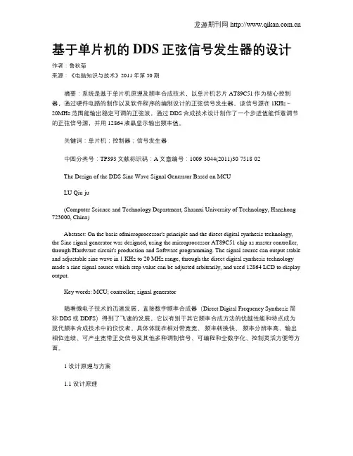
基于单片机的DDS正弦信号发生器的设计作者:鲁秋菊来源:《电脑知识与技术》2011年第30期摘要:系统是基于单片机原理及频率合成技术,以单片机芯片AT89C51作为核心控制器,通过硬件电路的制作以及软件程序的编制设计的正弦信号发生器。
该信号源在1KHz~20MHz范围能输出稳定可调的正弦波,通过DDS合成技术设计制作了一个步进值能任意调节的正弦信号源,并用12864液晶显示输出频率值。
关键词:单片机;控制器;信号发生器中图分类号:TP393文献标识码:A文章编号:1009-3044(2011)30-7518-02The Design of the DDS Sine Wave Signal Generator Based on MCULU Qiu-ju(Computer Science and Technology Department, Shaanxi University of Technology, Hanzhong 723000, China)Abstract: On the basis ofmicroprocessor's principle and the direct digital synthesis technology, the Sine signal generator was designed, using the microprocessor AT89C51 chip as master controller, through Hardware circuit's production and Software programming. The signal source can output stable and adjustable sine wave in 1 KHz to 20 MHz range, through the direct digital synthesis technology made a sine signal source which step value can be adjusted arbitrarily, and used 12864 LCD to display output.Key words: MCU; controller; signal generator随着微电子技术的迅速发展,直接数字频率合成器(Direct Digital Frequency Synthesis简称DDS或DDFS)得到了飞速的发展,它以有别于其它频率合成方法的优越性能和特点成为现代频率合成技术中的佼佼者。
1引言信号发生器是指产生所需参数的电测试信号的仪器。
按信号波形可分为正弦信号、函数(波形)信号、脉冲信号和随机信号发生器等四大类。
信号发生器又称信号源或振荡器,各种波形曲线均可以用三角函数方程式来表示。
能够产生多种波形,如三角波、锯齿波、矩形波(含方波)、正弦波的电路被称为函数信号发生器。
在生产实践和科技领域中有着广泛的应用。
信号发生器在电路实验和设备检测中具有十分广泛的用途。
例如在通信、广播、电视系统中,都需要射频(高频)发射,这里的射频波就是载波,把音频(低频)、视频信号或脉冲信号运载出去,就需要能够产生高频的振荡器[7]。
在工业、农业、生物医学等领域内,如高频感应加热、熔炼、淬火、超声诊断、核磁共振成像等,都需要功率或大或小、频率或高或低的振荡器。
正弦信号发生器的实现方法通常有以下几种:(1)用分立元件组成的信号发生器:通常是单函数发生器且频率不高,其工作不很稳定,不易调试。
(2)采用传统的直接频率合成法直接合成。
利用混频器、倍频器、分频器和带通滤波器完成对频率的算术运算。
由于采用大量的倍频、分频、混频和滤波环节,导致直接频率合成器的结构复杂,体积庞大,成本高,而且容易产生过多的杂散分量,难以达到较高的频谱纯度。
(3)采用锁相环间接频率合成 (Phase Lock Loop简称PLL)。
虽然具有工作频率高、宽带、频谱质量好的优点,但由于锁相环本身是一个惰性环节,锁定时间较长,故频率转换时间较长。
另外,由模拟方法合成的正弦波的参数(如幅度、频率和相位等)都很难控制,不易实现[2]。
(4)用专用直接数字合成(Direct Digital Synthesize r简称DDS)芯片的信号发生器:能产生任意波形并达到很高的频率。
用随机读/写存储器RAM存储所需波形的量化数据,按照不同频率要求,以频率控制字K为步进对相位增量进行累加,以累加相位值作为地址码读取存在存储器内的波形数据,经D/A转换和幅度控制,再滤波即可得所需波形。
毕业论文(设计)题目基于DDS的正弦波信号发生器设计学生姓名学号指导教师系部名称专业班级完成时间摘要DDS正弦波信号发生器能对输出电平进行调节,输出各种波形,把信号发生器的频率稳定度、准确度提高到与基准频率相同的水平,并且可以在很宽的频率范围内进行精细的频率调节。
在跳频技术、无线电通信技术方面有着重要作用。
传统的正弦波信号发生器大多是基于模拟电子技术设计制作的,这种信号源制作简单,成本低廉,但是它的缺点也很多,比如不便于存储,频率稳定度差,失真度高等。
DDS是以全数字技术,从相位概念出发直接合成所需波形的一种新的合成原理。
本设计采用DDS和单片机技术相结合,以DDS芯片AD9850为核心设计了一种幅度、相位、频率都可调节的正弦波信号发生器,它不仅能克服传统的正弦波信号发生器的缺点,而且由模拟乘法器产生调幅电路、采用数字键控的方法实现二进制PSK、ASK信号,且频带较宽、频率稳定度高,波形良好。
设计目标是用DDS芯片AD9850,产生0kHz~2mHz范围、频率步进1KHz可调、输出峰峰值在6 V的正弦波基本信号。
以AVR单片机Atmegal6为控制核心,结合FPGA辅助逻辑控制电路,对实现的正弦波基本信号进行幅度、频率、相位调制和调制度及频偏的程序控制。
以论文总体分为硬件设计部分,软件设计部分,仿真与测试部分。
并论文中详细进行介绍。
关键词:数字频率合成;FPGA;AVR单片机;信号调制;AD9850;AbstractThe design use DDS chip AD9850 to generate sine wave,whose frequency is from 0 Hz to 2 MHz,stepper is 1KHz and peak value is around 6 V.It use AVR MCU Atmega 16 as the control unit.MCU combine with assistant logic control circuit with FPGA which generate sin modulated signal of 1 kHz frequency and binary baseband serialsignal to control the peak,frequency,phase,modulate coeficient and frequency steppe r of sine wave with program.It has the virtue of wide baseband,high precision ,stabilization,low cost and fme interface.Th e production can use as realia and scientific research instnmaent.Key words:DDS;FPGA;AVR MCU;signal modulate目录摘要 (I)Abstract (II)第一章概述 (1)第二章方案论证 (1)2.1主控制器 (2)2.2正弦信号产生 (2)2.3输出电压放大 (2)2.4 FM调频电路 (3)2.5 AM调幅电路 (3)2.6产生二进制PSK、ASK信号 (3)第三章详细软硬件设计 (3)第四章硬件模块设计 (5)4.1 SPCE061A简介 (5)4.1.1 综述 (5)4.1.2 性能 (6)4.1.3 结构概览 (6)4.1.4芯片的引脚排列和说明 (7)4.2 正弦信号产生模块 (9)4.2.1 AD9850芯片简介 (9)4.2.2 AD9850工作方式介绍 (11)4.2.3相位控制字的计算 (11)4.3 带负载输出 (14)4.3.1推挽放大器 (15)4.4正弦调制信号的产生 (16)4.5 AM调幅信号的产生 (17)4.6 ASK、PSK的产生 (18)4.6.1 ASK: 幅移键控ASK (Amplitude Shift Keying) (18)4.6.2 PSK:数字相位调制(phase shift keying) (18)4.7 LCD显示器 (22)4.7.1 概述 (23)4.7.2 基本特性 (23)4.7.3 模块接口说明 (23)4.7.4 控制器信号接口说明 (24)第五章软件设计 (26)第六章测试说明 (27)参考文献 (29)附录 (30)致谢 (31)第一章概述● 1.1引言信号源作为一种信号产生的装置已经越来越受到人们的重视,它可以根据用户的要求,产生自己需要的波形,具有重复性好,实时性强等优点,已经逐步取代了传统的函数发生器。
基于DDS的正弦波信号发生器的设计DDS(Direct Digital Synthesis,直接数字合成)技术是一种通过数字计算得到各种波形信号的合成技术。
正弦波信号发生器是一种用于产生正弦波信号的电子设备,通常用于各种测量、实验和测试中。
本文将介绍基于DDS的正弦波信号发生器的设计。
1.设计目标我们的设计目标是开发一个基于DDS的正弦波信号发生器,具有以下特点:-可以生成多种频率的正弦波信号;-可以通过数字控制方式调整频率;-可以输出稳定的、低失真的正弦波信号。
2.设计思路-选择一个固定的时钟频率作为DDS系统的时钟频率;-使用一个相位累加器来产生一个递增的相位值,该相位值与输出的正弦波信号频率相关;-使用一个查表ROM存储正弦波的采样值,根据相位值从查表ROM中读取相应的采样值;-使用一个数字到模拟转换器(DAC)将采样值转换成模拟信号输出。
3.系统设计基于上述思路,我们可以设计一个基于DDS的正弦波信号发生器,具体步骤如下:-设计一个用于控制频率的数字控制模块。
该模块可以接收一个控制信号,根据控制信号计算应当输出的频率,并将频率值传递给相位累加器。
-设计一个相位累加器模块。
该模块可以接收一个时钟信号和一个频率值,并根据时钟信号和频率值递增相位值,并将相位值传递给查表ROM模块。
-设计一个查表ROM模块。
该模块可以接收一个相位值,并根据相位值从查表ROM中读取相应的采样值。
-设计一个数字到模拟转换器(DAC)模块。
该模块可以接收一个采样值,并将采样值转换成模拟信号输出。
4.系统性能考虑在设计基于DDS的正弦波信号发生器时,需要考虑一些性能指标以确保输出的信号质量,如下所示:-频率范围:选择合适的时钟频率和相位累加器实现合理的频率范围。
-分辨率:根据需要的输出信号精度选择合适的查表ROM大小和DAC分辨率。
-失真度:选择合适的查表ROM分辨率和DAC精度,以及合适的滤波器设计,以保证输出信号的低失真度。
基于LMP核和DDS的正弦波函数发生器设计摘要:在频率合成领域中,直接数字合成(DDS)是近年来新的技术,它是从相位概念出发直接合成所需波形的一种新的全数字技术的频率合成方法。
此次正弦波函数发生器的设计是利用VHDL语言和Quartus II开发环境进行设计。
首先对VHDL和Quartus II开发环境进行了介绍,接着对DDS工作原理进行了阐述,最后提出了两种方法并进行了比较和做出了选择。
关键词:DDS;正弦波函数发生器;VHDL;Quartus II1.前言1.1 课题研究背景在一些电子设备的电路板故障检测仪中,往往需要频率、幅度都能由计算机自动调节的信号源。
采用诸如MAX038信号发生器芯片外加电阻及切换开关等器件虽然也能调节频率和幅度,但这种调节是离散的,且电路复杂,使用不方便。
而采用直接数字合成芯片DDS及外加D/A转换芯片构成的可控信号源,可产生正弦波、调频波、调幅波及方波等,并且其信号的频率和幅度可由微机来精确控制,调节非常方便。
另外随着21世纪的到来,人类正在跨入信息时代。
现代通信系统的发展方向是功能更强,体积更小,速度更快,功耗更低。
1.2 课题研究目的和意义正弦信号发生器作为电子技术领域中最基本的电子仪器,广泛应用于航空航天测控、通信系统、电子对抗、电子测量、科研等各个领域中。
随着电子信息技术的发展,对其性能的要求也越来越高,如要求频率稳定性高、转换速度快,具有调幅、调频、调相等功能,另外还经常需要两路正弦信号不仅具有相同的频率,同时要有确定的相位差。
随着数字信号处理和集成电路技术的发展,直接数字频率合成(DDS)的应用也越来越广泛。
DDS具有相位和频率分辨率高、稳定度好、频率转换时间短、输出相位连续、可以实现多种数字与模拟调制的优点,而可编程门阵列(FPGA)具有集成度高、通用性好、设计灵活、编程方便、可以实现芯片的动态重构等特点,因此可以快速地完成复杂的数字系统。
由于模拟调相方法有生产性差、调试不方便、调制度控制不精确等缺点,因此采用数字方法实现各种模拟调制也越来越普遍。
Sine signal generator design based on DDS 作者: 洪远泉;夏新恩;吴丽珠
作者机构: 韶关学院信息工程学院,广东韶关512005
出版物刊名: 韶关学院学报
页码: 53-57页
主题词: 数字频率合成;FPGA;AVR单片机;信号调制
摘要:采用DDS芯片AD9851,产生1kHz~10mHz范围、频率步进100Hz可调、输出峰峰值在6v的正弦波基本信号,以AVR单片机Atmega16为控制核心,结合腓A辅助逻辑控制电路(产生1kHz的正弦调制信号和二进制基带序列信号),对实现的正弦波基本信号进行幅度、频率、相位调制和调制度及频偏的程序控制.该设计具有频带宽、精度高、性能稳定、成本低和操作界面友好等特点.可作为教具和科研用仪器.。
毕业设计文献综述电子信息科学与技术基于FPGA的DDS信号发生器设计摘要:讨论了DDS信号发生器的原理及性能特点,简单介绍了实现该技术的几种方式,以及几种方案的比较。
关键字:直接数字频率合成器(DDS);FPGA;0、引言传统的信号波形产生方法,如RC和LC振荡器或单片模拟集成函数发生器,尽管它们的电路实现比较简单,但产生的信号波形频率精度和稳定度并不是很理想,而使用锁相环技术,频率精度有了很大的提高,但工艺相对比较复杂,分辨率也不高,频率变换和实现计算机程序控制也不方便。
随着电子技术的迅速发展,一种全新的信号合成技术,即直接数字频率合成技术,将先进的数字信号处理理论与方法引入信号合成领域,实现了合成信号的频率转换和频率准确度之间的统一。
DDS以其优越的性能特点成为现代频率合成技术中的佼佼者,被广泛应用于跳频通信、雷达、导航、电子侦察、干扰和反干扰等电子技术领域,具有很高的研究价值。
1、DDS的原理及性能特点DDS是一种从相位概念出发直接合成所需波形的数字频率合成技术,主要通过查波形表实现。
由所学过的奈奎斯特抽样定理可知,当抽样频率大于被抽样信号的最高频率2倍时,通过抽样得到的数字信号可以通过一个低通滤波器还原成原来的信号。
DDS信号发生器主要由参考时钟、相位累加器、波形存储器、D/A转换器和模拟低通滤波器组成(如图1)。
图1 DDS原理结构图图2 相位累加器由图1可知,在参考时钟fs 的控制下,频率控制字k 与相位寄存器的输出反馈经累加器完成加运算,并把计算结果寄存于相位寄存器,作为下一次加运算的一个输入值。
而相位累加器输出高位数据作为波形存储器(即图中的ROM 表)的相位地址值,用于查找波形存储器中相对应单元的电压幅值,得到波形二进制编码。
波形二进制编码再通过D /A 转换器,把数字信号转换成模拟信号。
低通滤波器可进一步滤除模拟信号中的高频成分,使输出的模拟信号更平滑。
在整个过程中,当相位累加器完成一次加运算并输出时,DDS 系统就完成一个周期输出任务,所以DDS 输出频率和频率分辨率为()s N o f kf 2= 输出频率 N s o f f 2=∆ 频率分辨率式中,k 为频率控制字;fs 为参考时钟,N 为相位累加器的位宽。
DDS devices to produce high-quality waveform: a simple, efficient and flexibleAbstract: Direct digital frequency synthesis (DDS) technology for the generation and regulation of high-quality waveforms, widely used in medical, industrial, instrumentation, communications, defense and many other areas. This article will briefly describe the technology, on its strengths and weaknesses, examine some application examples, and also introduced some new products that contribute to the promotion1.IntroductionA key requirement in many industries is an exact production, easy operation and quick change of different frequencies, different types of waveforms. Whether it is broadband transceiver requires low phase noise and excellent spurious-free dynamic performance of agile frequency source, or for industrial measurement and control system needs a stable frequency excitation, fast, easy and economical to produce adjustable waveform while maintaining phase continuity capabilities are critical to a design standard, which is what the advantages of direct digital frequency synthesis.2.Frequency synthesis taskThe growing congestion of the spectrum, coupled with lower power consumption, quality of never-ending demand for higher measuring equipment, these factors require the use of the new frequency range, requires a better use of existing frequency range. A result, the search for better control, in most cases, by means of frequency synthesizer for frequency generation. These devices use a given frequency, fC of to generate a target frequency (and phase) fOUT the general relationship can be simply expressed as:fOUT = εx× fCAmong them, the scale factor εx, sometimes known as the normalized frequency.The equation is usually gradual approximation of the real number algorithms. When the scale factor is a rational number, two relatively prime numbers (output frequency and reference frequency) than the harmonic. However, in most cases, εx may belong to a broader set of real numbers, the approximation process is within the acceptable range will be truncatedThe frequency synthesizer a practical way to achieve is the direct digital frequency synthesis (of DDFS), usually referred to as direct digital synthesis (DDS). This technique using digital data processing to generate a frequency and phase adjustable output, the output anda fixed frequency reference clock source fC. related. DDS architecture, the reference or the system clock frequency divided by a scale factor to produce the desired frequency, the scale factor is controlled by the binary tuning word programmable.In short, direct digital frequency synthesizer to convert a bunch of clock pulses into an analog waveform, usually a sine wave, triangle wave or square wave. Shown in Figure 1, its main parts: the phase accumulator (to produce the output waveform phase angle data), relative to digital converter, (above the phase data isconverted to the instantaneous output amplitude data), and digital-to-analog converter (DAC) (the magnitude of data into a sampled analog data points)Figure 2-1 DDS function of the system block diagram.For the sine wave output, relative to digital converter is usually a sine lookup table (Figure 2). Phase accumulator unit count N a relative to the frequency of fC, according to the following equation:The number of pulses of the fC:M is the resolution of the tuning word (24-48)N corresponds to the smallest increment of phase change of the phase accumulator output wordFigure2-2 Typical DDS architecture and signal path (with DACs).Changing N will immediately change the output phase and frequency, so the system has its own continuous phase characteristics, which is one of the key attributes of many applications. No loop settling time, which is different from the analog system, such as phase-locked loops (PLLs). DAC is usually a high-performance circuit, designed specifically for the DDS core (phase accumulator and phase amplitude converter). In most cases, the results of the device (usually single-chip) is generally referred to as the pure DDS or the C-DDS.Actual DDS devices are generally multiple registers, in order to achieve a different frequency and phasemodulation scheme. Such as phase register, their storage phase of increase in the output phase of the phase accumulator. In this way, the corresponding delay output sine wave phase in a phase tuning word. This is useful for phase modulation applications for communication systems. The resolution of the adder circuit determines the number of bits of the phase tuning word, therefore, also decided to delay the resolution.Integrated in a single device on the engine of a DDS and a DAC has both advantages and disadvantages, however, whether integrated or not, need a DAC to produce ultra-high purity high-quality analog signal. DAC will convert digital sinusoidal output to an analog sine wave may be single-ended or differential. Some of the key requirements for low phase noise, excellent wideband (WB) and narrowband (NB), spurious-free dynamic range (SFDR), and low power consumption. If the external device, the DAC must be fast enough to handle the signal, so the built-in parallel port device is very common.3.DDS and other solutionsThe frequency analog phase-locked loops (PLLs), clock generator, and the use of FPGA dynamic programming of the output of the DAC. By examining the spectrum of performance and power of these technologies, a simple comparison, Table 1 shows the qualitative results of the comparisonTable 3-1DDS with competing technologies - Advanced comparePower consumption Spectral purity RemarksDDS Low Middle Ease of tuningDiscrete DAC+FPGA Middle Middle-High With tuning capabilitiesAnalog PLL Milddle High Difficult tuningPhase-locked loop is a feedback loop and its components: a phase comparator, a divider and a pressure-controlled oscillator (VCO), phase comparator reference frequency and output frequency (usually the output frequency is N)frequency) were compared. The error voltage generated by the phase comparator is used to adjust the VCO, thus the output frequency. When the loop is established, the output frequency and / or phase with the reference frequency to maintain a precise relationship. PLL has long been considered in a particular frequency range, high fidelity and consistent signal low phase noise and high spurious free dynamic range (SFDR) are ideal for applications.PLL can not be precisely and quickly tuning the frequency output waveform, and the slow response, which limits their applicability for fast frequency hopping and part of the frequency shift keying and phase shift keying applications.Other programs, including integrated DDS engine field programmable gate arrays (FPGAs) - a synthetic sine wave output with the off-the-shelf DAC - though the PLL frequency-hopping problem can be solved, but there own shortcomings. The defects of the major systems work and interface power requirements, high cost, large size, and system developers must also consider the additional software, hardware and memory. For example, using the DDS engine option in the modern FPGA to generate the 10 MHz output signal dynamic range is 60 dB up to 72 kB memory space. In addition, designers need to accept and be familiar with thesubtle balance DDS core architecture. .From a practical point of view (see Table 2), thanks to the rapid development of CMOS technology and modern digital design techniques, as well as the improvement of the DAC topology, DDS technology has been able to achieve unprecedented low power consumption in a wide range of applications, spectrum performance and cost levels. Although the pure DDS products in performance and design flexibility to achieve the level of high-end DAC technology and FPGA, but the advantages of DDS in terms of size, power consumption, cost and simplicity, making it the primary choice for many applications.Table 3-2 Benchmark Analysis Summary - frequency generation technique (<50 MHz)Phase -locked loop DAC + FPGA DDS Spectral performance High High MiddleSystem power requirements High High MiddleDigital frequency tuning No Yes YesTuning response time High Low LowSolution size Middle High LowWaveform flexibility Low Middle HighCost Middle High LowDesign reuse Middle Low HighImplementation complexity Middle High LowAlso be noted that the DDS device for digital methods to produce the output waveform, it can simplify some of the architecture of the solution, or the waveform of digital programming to create the conditions. Usually with a sine wave to explain the functions and working principle of the DDS, but using modern DDS ICs can easily generate a triangle wave or square wave (clock) output, thereby eliminating the former case the lookup table, and the latter case the DAC the need to integrate a simple and accurate enough.4. Performance and limitations of the DDS4.1 Image and envelope: Sin (x) xx roll-offThe actual output of the DAC is not a continuous sine wave, but a series of pulses with a sinusoidal time envelope. The corresponding spectrum is a series of image and signal aliasing. Image along the sin (x) / x envelope distribution (see Figure 3 | margin | graph). The need for the filter to suppress frequencies outside the target band, but can not inhibit the high-level in the passband aliasing (for example, caused due to DAC non-linear)The Nyquist criterion requires that each cycle requires at least two sampling points in order to rebuild the desired output waveform. The Mirroring response arising from sampling the output frequency K, CLOCK ×OUT In this example, which CLOCK = 25 25 MHz and fOUT = 5 MHz, the first and second mirror frequency appear in (see Figure 3) fCLOCK × fOUT, o 20 MHz and 30 MHz. The third and fourth mirror frequency at 45 MHz and 55 MHz. Note, sin (x) / x value of zero at multiples of the sampling frequency.When fOUT greater than the Nyquist bandwidth (1/2 f CLOCK), the first mirror frequency will appear in the Nyquist bandwidth, the occurrence of aliasing (such as 15 MHz signal aliasing down to 10 MHz). Can not use the traditional quist anti-aliasing filter to filter out aliasing mirror frequency from the outputFigure 4-1 Sin, in Figure 3.DDS, (x) / x roll-off.In a typical DDS application, the use of a low-pass filter to suppress the mirror frequency response of the output spectrum. To make the low-pass filter cutoff frequency to remain at reasonable levels, and keep it simple filter design, a feasible approach is the use of an economic low-pass output filter bandwidth limited to about 40% of the frequency of clock.Any given mirror frequency relative to the amplitude of the fundamental formula of sin (x) / x calculation. Because the function of the frequency roll-off, the basic output of the amplitude and the output frequency is inversely proportional to decrease; in the DDS system, reduce the amount of DC-Nyquist bandwidth range of -3.92 dB.Significant reduction in frequency in the first mirror - the fundamental 3 dB range. In order to simplify the DDS application filtering, frequency plan must be formulated and analyzed to mirror the frequency and magnitude of the sin (x) / x response in the OUT and CLOCK target frequency spectrum requirements. Other unwanted frequencies in the output spectrum (such as integral and differential linearity error of the DAC, the surge of energy associated with the DAC and clock feed through noise) does not follow the sin (x) / x roll-off response. These unwanted frequencies will be harmonic and spurious energy in the output spectrum in many places - but its magnitude is generally far below the mirror frequency response. DDS devices to the general background noise, substrate noise, thermal noise effects, ground coupling and other signal source coupling factor cumulative portfolio decisions. DDS devices, the noise floor performance of stray and jitter by the circuit board layout, power quality, and - most importantly - Enter the profound impact of the quality of the reference clock.4.2ShakeThe edge of the perfect clock source will be the precise time interval, the interval will never change. Of course, this is not possible; even the best oscillator is also the ideal components constitute, with noise and other defects. Quality and low phase noise crystal oscillator jitter picosecond, and is built up from one millionthe number of clock edge. The factors leading to jitter external interference, thermal noise, the oscillator circuit instability and power, ground and output connections bring, all these factors will interfere with the timing characteristics of the oscillator. In addition, the oscillator by the external magnetic field or electric field and the nearby transmitter RF interference. Oscillator circuit, a simple amplifier, inverter or buffer to signal additional jitter.Therefore, the choice of a low-jitter, and the edge of steep stable reference clock oscillator is critical. Higher frequency reference clock allows a larger sample, and divide to some extent, reduce the jitter, because the signal to divide a long time to produce the same amount of jitter, which can reduce the jitter on the signal percentage.4.3 Noise - including the phase noiseThe sampling system noise depends on many factors, the most important factor is the reference clock jitter, this jitter performance of phase noise on fundamental signal. In the DDS system, the register output of the truncated phase may bring the system error code. The binary word does not lead to the truncation error. But for non-binary word, phase noise truncation error in the spectrum spurious. Spurious frequency / amplitude depends on the code word. Quantification and linearity error of the DAC will be brought to the system harmonic noise. Time-domain error (such as owed to the red / overshoot and code errors) will increase the output signal distortion.5. Application5.1 DDS applications can be divided into two categories:Require agile frequency source for data coding and modulation applications, communications and radar systemsRequire measurement of the universal frequency synthesizer features and programmable tuning, scanning, and motivational skills, industrial and optical applicationsBoth cases, the trend toward higher spectral purity (low phase noise and higher spurious free dynamic range), also low power and small size requirements to accommodate the remote ordemand for battery-powered devices.5.2 Modulation / data encoding, and synchronization of the DDSDDS products first appeared on the radar and military applications and the development of some of its characteristics (performance improvements, cost and size, etc.) DDS technology is becoming more prevalent in the modulation and data encoding applications. This section will discuss the two data encoding scheme in the DDS system.5.3 Binary frequency shift keyingThe launch of the data is a continuous carrier frequency in two discrete frequency (binary one, ie, pass number, a binary 0, namely, the transformation between the space). Figure 4 shows the relationship between the data and transmit signals.Figure 5-1 binary FSK modulation.Binary 1 and 0 for two different frequencies f0 and f1, respectively. This encoding scheme can be easily DDS device. On behalf of the output frequency of the DDS frequency tuning word change to f0 and f1, will launch the 1 and 0. To transform the output frequency shall dedicated pin FSELECT, containing the appropriate tuning word registers (see Figure 5)Figure 5-2 AD9834 or AD9838 DDS tuning word selector realization of the FSK encoding.5.4 Phase shift keying (PSK)In PSK, the carrier frequency remains the same, by changing the phase of the transmitted signal to transmit information. Can take advantage of a variety of programs to achieve PSK,. The easiest way is often referred to as binary PSK (BPSK), using only two signal phase: 0 ° (logic 1) and 180 ° (logic 0). Members state depends on the status of the former one. If the wave phase remains unchanged, the signal state will remain the same (low or high). Wave phase change 180 °, ie, phase inversion, the signal state will change (low into high or high to low). PSK coding in DDS products can be easily achieved, because most devices have a separate input register (phase register), and phase values can be loaded. This value is added directly to the carrier phase, without changing its frequency. Change the contents of the register will be modulated carrier phase, resulting in a PSK output. For applications that require high-speed modulation, built-in phase register of the AD9834 and AD9838 allow PSELECT pin signal transformation, according to need modulated carrierin the preloaded phase registers.The more complex the PSK four or eight-wave phase. Thus, whenever the phase change of binary data transfer rate will be higher than the BPSK modulation. In the four-phase modulation (Quadrature PSK), in the phase angle of 0 ° to +90 °, -90 ° and +180 °; each phase to transform the two signals may represent a factor AD9830, AD9831, AD9832, and the AD9835 provides four phase registers, can be continuously updated register of different phase shift, the complex phase modulation scheme.5.5 The use of synchronous mode of multiple DDS devices to achieve the I / QMultiple DDS components to achieve the many applications of the I / Q sine wave or square wave signal of known phase relationship between two or more synchronous mode. A common example is the same phase and quadrature modulation (I / Q) in this technique, the phase angle of 0 ° and 90 ° from the carrier frequency signal information. To run two separate DDS components, you can use the same source clock to output can directly control and manipulate the signal of the phase relationship. In Figure 6, with a reference clock on the AD9838 device programming; the RESET pin is used to update the two devices. In this way, you can achieve a simple I / Q modulationRESET after power and initialized before any data to the DDS transmission. DDS output results can be placed in a known phase, making it a common reference point of view, in order to synchronize multiple DDS devices. When new data is sent to multiple DDS devices, the DDS can remain relevant phase relationship, or by the phase offset register can predict the relative phase shift between the adjustments of multiple DDS. The AD983x series of DDS products have a 12 phase resolution, the effective resolution of 0.1 °.Figure 5-3 Synchronize the two DDS components.DDS器件产生高质量波形:简单、高效而灵活摘要:直接数字频率合成(DDS)技术用于产生和调节高质量波形,广泛用于医学、工业、仪器仪表、通信、国防等众多领域。