1000W数字功放
- 格式:pdf
- 大小:298.89 KB
- 文档页数:1


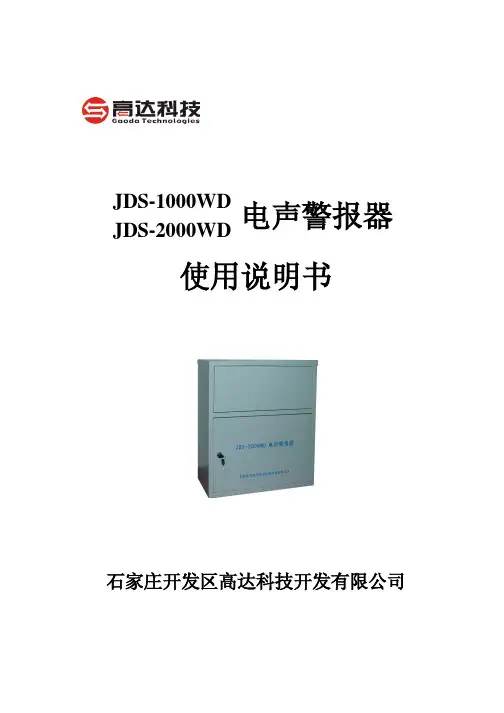
JDS-1000WD电声警报器JDS-2000WD使用说明书石家庄开发区高达科技开发有限公司目录1.JDS系列电声警报器产品简介: (2)2.功能特点 (2)3.警报器的安装与使用 (2)3.1.警报器的安装 (2)3.2.警报器的使用 (3)4.警报器前面板按键功能及操作 (4)4.1.电源开关、键盘锁、监听、警报、语音及充电按键的使用 (4)4.2.液晶各功能菜单的操作 (5)5.警报器的输入输出接口 (7)5.1.卧式机型 (7)5.2.壁挂机型 (7)6.技术指标 (8)6.1.JDS-1000WD型技术指标 (8)6.2.JDS-2000WD型技术指标 (9)1.JDS系列电声警报器产品简介:JDS-系列电声警报器分为1000W和2000W两种类型,型号分别为JDS-1000WD和JDS-2000WD。
并具有4U卧式和壁挂式两种外形供用户选择。
该系列警报器采用全数字化结构:电源采用开关电源,核心控制单元采用高速、高性能单片机,功放为大功率D类数字功放,采用大屏幕液晶显示以及数字遥控接口。
该警报器具有功能强大、结构简单、工作可靠、兼容性好、外观优美等优点。
2.功能特点l采用模块化设计,结构简单,工作可靠,维护方便。
l有卧式和壁挂式外形,适合各种场合。
l采用开关电源,效率高,重量轻,电源适应范围宽。
l采用D类数字功放,最大输出功率达2000W,功放效率达90%以上。
l警音采用单片机软件编程产生,音质纯净、信噪比高,警音频率和变调周期稳定。
l数控音量调节,避免了音量电位器接触不良造成的故障。
l警音自动优先控制,各种音源智能切换,遥控警报时音量自动调节至最大,遥控警报稳定可靠。
l具有自检功能,可对电源状态、电池状态,音源状态、功放状态、扬声器状态进行全面检测,并可将检测情况通过有线/无线发回中心站,方便远程遥测。
l扬声器检测不扰民,可经常性对警报器检测,确保警报器状态良好。
l可独立发放各种警报、录音,并可作为扩音机使用。
目录目录 (i)摘要 (iii)Abstract (iv)1数字集成功率放大器设计概述 (1)2数字集成功率放大器整体电路设计 (2)2. 1输入切换部份的设计 (2)2.1.1 TC9152P组成电路图 (2)2.1.2TC9152P应用电路说明 (3)2.1.3TC9152P要紧元件参数说明 (4)数字音量操纵部份设计 (4)2.2.1TC9153组成电路图 (4)2.2.2TC9153应用电路说明 (5)2.2.3 TC9153要紧元件参数说明 (5)2.2.4 TC9153组成电路的屏蔽 (5)功率放大器部份设计 (5)2.3.1 TDA7481的特点 (6)2.3.2 TDA7481的引脚及参数说明 (7)2.3.3 TDA7481的外围电路 (8)2.3.4TDA7481的相关计算 (8)电源部份电路设计 (9)3设计总电路图 (12)4结论 (13)参考文献 (14)致谢 (15)附录 (15)摘要本设计采纳TDA7481芯片组成的数字集成功率放大器,加入了音源选择电路,该选择器能够在TUNER、TAPE、CD、AUX一、AUX2之间任意切换,大大方便了整机的适用性。
另外在音量操纵部份已改传统电位器操纵的做法,选用了数字轻触式按键操纵,如此能够方便操作和延长寿命。
由于选用D类功率放大器,其输出功率大、效率较高、失真较小,使整机具有了很多良好的性能。
关键词:TDA7481;效率;D类功率放大器AbstractThis design used the TDA7481 chip composing the digital integration power amplifier, joined the sound source selecting circuit which contain TUNER, TAPE, CD, AUX1 and AUX2,and then it greatly improved the applicability of the equipment. Another, at the part of volume controlling, in order to simplify the operation and last its life, the traditional potentiometer controlling was changed into digital button-click controlling. Because of the Class-D amplifier assembled, and its high power of output, high efficiency, and small distortion, the whole equipment has many good performances.Key words: TDA7481;efficiency;Class-D amplifier asembled1数字集成功率放大器设计概述该集成功率放大器是集成了数字音量操纵(TC9153),音源选择(TC9152P)的D 类功率放大器,功率放大部份选用TDA7481。
LA4功率放大控制器2.0版本1 安全警告适用于L-ACOUSTICS LA4功率放大控制器的所有详细的信息,在此部分都以“此产品”代替。
1.1 符号说明1.1.1 手册使用的符号本手册中潜在的危险用以下的符号表示:闪电符号表明遭受电击会有生命危险。
此外,产品也会受到严重的破坏。
电压警告符号表明太靠近产品可能会对用户或他人产生危险。
此外,产品也可能受损。
小心符号旨在提醒用户相关的信息以防产品可能发生损坏。
重要符号表示的是关于产品使用的重要建议。
1.1.2 产品上的符号由于产品是电子设备,使用者会有潜在的危险。
因此用户必须十分注意标示在产品盖子的符号:靠近NL4FC Speakon ®连接头插座的闪电符号表示产品会产生很高的输出电压,用户有潜在的生命危险。
本产品和音箱的连接需要用一个现成的导线。
当功放正在操作时,切勿在没有拔掉本 产品的连接头的情况下触摸任何音箱的明线。
1.2 重要安全指示1. 阅读本用户手册2. 留意所有的安全警告3. 遵循所有的指示4. 用户切勿使用没有得到L-ACOUSTICS®认可的设备或者配件5. 环境只能在符合EN55103-2标准的E1,E2,E3,E4环境下使用本产品。
电压电压电压6. 无线电干扰本产品的样机已经经过测试并符合EMC指示的限制规定。
这些限制意在对产品提供合理的保护,使产品免受电气设备产生的有害干扰。
尽管如此,在特定安装的情况下,干扰还是有可能发生的。
7. 电源线保护电源线损坏或发生磨损时,切勿使用本产品。
电源线必须妥当安置,避免受到踩踏或重物压下,尤其是插头和从功放拉线出来的位置。
8. 交流电源在120/230V,50-60Hz的交流电下使用本产品。
日本为100V,50-60Hz。
9. 接地本产品只能通过使用交流电的接地插座连接,切勿损坏插座的接地脚。
如果当地的插座老旧,请联系合格的电工进行维修。
本产品适合使用接地插头;切勿损坏连接母插头到本产品底盘的接地线。

专业音响中术语解释超低音音箱(Subwoofer)指用于重放那些深沉的而由普通小型音箱所无法予以重放出来的低频段的特制音箱。
唱臂(Tonearm)为唱机的一部分,其上装有唱头。
瞬态(Transient)指乐曲(特别是打击乐)中那些短暂而有爆发性的声音,通常,这些声音是难于准确重放出来的。
三线分音(推动)(Triamping/Triwiring)指与双线分音(biwiring)及双功放推动(biamping)相类似的一种功放与音箱的连接方式,不过此时需使用三对喇叭线/或三台功放,而且仅适用于三分频并带相应输入端子的音箱。
抖晃(Wow)指录音机或录音座转速的缓慢变化所导致产生的不稳定的畸形声音。
AAD指录音及后期制作皆为模拟(A)方式,而只有制片使用数字(D)方式的CD唱片制作。
A/B试听比较(A/B comparison)指对两种不同的音乐重放方式进行的反复试听比较。
绝对极性(absolute polarity)在用绝对极性正确的音响系统播放绝对极性正确的录音制品时,音箱所产生的正向声压便会和原始声音的正向声压一致。
绝对极性不对时,便会有180°的相位差。
对于有些乐器,有些人是能听出绝对极性的正确与否的。
电源净化器(AC line-conditioner)指专门用来滤去交流供电电源中的噪声和防止音响器材受到电压峰值和浪涌损害的一种音响辅助器材。
有些电源净化器甚至还可用来防止闪电的损伤。
其实,电源净化器便是一种特别设计和制作的滤波器。
吸声材料(acoustic absorbed)指任何一种能够吸收声波的材料,比如地毯、窗帘以及盖以厚实布套的家俱等等。
声扩散器(acoustic diffuser)指任何能够扩散声波的材料或器件。
声反馈(acoustic feedback)音箱发出的声音会使LP唱盘、话筒等拾音设备产生振动,此振动又被变换为电信号,并再次由音箱重放出来。
在这种反馈过程中,振动因自身的反馈而会越来越加强。
HIGH POWER PROFESSIONAL DIGITAL AMPLIFIERSPKNC XE2500PKNC XE4000PKNC XE6000 Name Professional power amplifierPower requirements160V – 270 VAC, (50-60Hz)Max. power consuption2600W 5500W 7900W Soft starting yesPower supply High frequency resonant includes active PFCMains connection NEUTRIK POWERCONWorking temperature range 0 - 40CStorage temperature range -25C - 60COutput power @ 8 Ohms 700W + 700W 1300W + 1300W 1900W + 1900W Output power @ 4 Ohms 1300W + 1300W 2100W + 2100W 3650W + 3650W Minimum load impedance 2 OhmFrequency ( +/- 3dB , 8Ohm ) 5Hz - 20KHzSlew rate 50V / us 60V / us Damping factor 400 500 600 End stages High frequency semi soft switched PWM in balanced configuration Output connections Four pole NEUTRIK SPEAKON (1+2+ in parallel,1-2- in parallel) Signal to Noise ratio A-Weighted 20Hz-20KHz 100 dB 102 dB 107 dB Nominal sensitivity for maximum output level (balanced) 1.4V (rms) 1.7V (rms) 1.7V (rms) Input impedance (referred to ground) 10KOhm +10KOhm (+/- 1%)Input terminals NEUTRIK XLRBuilt in limiter Programmable limiterOutput level meter Ledbar, status ledsDisplay Graphics LCDControl terminals JOGs, buttonsVolume control Set by control jog wheels or remote -95,5dB – 0dB (in 0.5dB steps) Input sensitivity -95.5dB – 0 dB (steps 0.5 dB)Limiter settings range 10 - 100 V10 - 155 V10 - 170 V User profiles 5 user profileProtections Short circuit,Overload,low impedance,thermal,DC fault Cooling Forced air cooling with regulated DC fans Direction of air flow Front to rearRemote control 10/100 Mps ETHERNETWeight 8 Kg 9 Kg 9.5 Kg External dimensions 19” rack 483mm * 440mm * 44mm (1RU)PKNC XD2500PKNC XE4000PKNC XE6000 Name Professional power amplifierPower requirements 160V – 270 VAC, (50-60Hz)Max. power consuption 2600W 5500W 7900W Soft starting yesPower supply High frequency resonant includes active PFCMains connection NEUTRIK POWERCONWorking temperature range 0 - 40CStorage temperature range -25C - 60COutput power @ 8 Ohms 700W + 700W 1300W + 1300W 1900W + 1900W Output power @ 4 Ohms 1300W + 1300W 2100W + 2100W 3650W + 3650W Minimum load impedance 2 OhmFrequency ( +/- 3dB , 8Ohm ) 5Hz - 20KHzSlew rate 50V / us 60V / us Damping factor 400 500 600 End stages High frequency semi soft switched PWM in balanced configuration Output connections Four pole NEUTRIK SPEAKON (1+2+ in parallel,1-2- in parallel) Signal to Noise ratio A-Weighted 20Hz-20KHz 100 dB 102 dB 107 dB Nominal sensitivity for maximum output level (balanced) 1.4V (rms) 1.7V (rms) 1.7V (rms) Input impedance (referred to ground) 10KOhm +10KOhm (+/- 1%)Input terminals NEUTRIK XLRBuilt in limiter yesOutput level meter Ledbar, status ledsControl terminals Two knobsInput sensitivity -95.5dB – 0 dB (steps 0.5 dB)User profiles 5 user profileProtections Short circuit,Overload,low impedance,thermal,DC fault Cooling Forced air cooling with regulated DC fans Direction of air flow Front to rearRemote control -Weight 8 Kg 9 Kg 9.5 Kg External dimensions 19” rack 483mm * 440mm * 44mm (1RU)PKNC LC2002PKNC LC4004 Name Professional power amplifierPower requirements 160V – 270 VAC, (50-60Hz)Max. power consuption 12 A 20 ASoft starting yesPower supply High frequency resonant includes active PFCMains connection NEUTRIK POWERCONWorking temperature range 0 - 40CStorage temperature range -25C - 60COutput power @ 8 Ohm 2 x 500W 4 x 500W Output power @ 4 Ohm 2 x 1000W 4 x 1000W Minimum load impedance 2 OhmFrequency ( +/- 3dB , 8Ohm ) 5Hz - 22KHzSlew rate 50V / usDamping factor 400 500End stages High frequency semi soft switched PWM in balanced configuration Output connections Four pole NEUTRIK SPEAKON (1+2+ in paralell, 1-2- in paralell) Signal to Noise ratio A-Weighted 20Hz-20KHz 104 dB 104 dB Nominal sensitivity for maximum output level (balanced) 700mV (rms) 700mV (rms)Input impedance (referred to ground) 10KOhm +10KOhm (+/- 1%)Input terminals NEUTRIK XLRBuilt in limiter yesCrossover 100 Hz Hi-pass filter, 120 Hz Lo-pass filter, 160 Hz Lo-pass filter Output level meter status LEDsProtections Short circuit, Overload, low impedance, thermal, DC fault Cooling Forced air cooling with regulated DC fans Direction of air flow Front to rearBridged configuration ability yesRemote control -Weight 6 Kg 8 Kg External dimensions 19” rack 483mm * 440mm * 44mm (1RU)PKN ControlsDISTRIBUTOR。
音响专业术语音响专业术语平衡(balance):指在音频频谱的高段和低段之间在相对响度上所存在的客观关系;也指双声道立体声左声道和右声道之间的信号的相同(平衡)。
平衡连接(balanced connection):指音响器材间的一种连接方式,在单根电缆中有3根导线,一根用来传送音频信号,另一根用于传送极性相反的音频信号,而另一根则为地线。
香蕉插座(banana jack)指装于音箱和功率放大器上用于和音箱线的香蕉插头连接的一种小型圆状插座。
香蕉插头(banana plug):普遍装于音箱线两端的供插入香蕉插座的一种插头。
带宽(band width):指音响装置能够处理或通过的一段频率范围。
比方说,杜比环绕声的环绕声道的带宽便是100Hz-7kHz。
环绕声道只通过频率在100Hz (低音)和7kHz(高音的低段)之间的频率。
人耳能听到的频率范围为20Hz-20kHz。
在谈到电气或声学器材的带宽时,往往指-3dB之间的频率范围。
低音(bass):指在音频低段的声音,通常低于500Hz(另一说则指低于160Hz)。
低频延伸(bass extension):指音响器材所能重放的最低频率。
系用于测定在重放低音时音响系统或音箱所能下潜到什么程度的尺度。
比方说,小型超低音音箱的低频延伸可以到40Hz,而大型超低音音箱则下潜到16Hz。
低音管理(bass management):指A/V功放接收机或A/V前置放大器中的综合控制电路,系用于确定应该给相应的音箱送去多少低频信号。
倒相式音箱(bass reflex):也称倒相式开孔箱,系在音箱面板上开有倒相孔(槽)的一类音箱。
由于开有孔,箱内的声音便可以辐射到外面来。
倒相式音箱比密闭式音箱的低频延伸要好些,但低音往往不那么结实紧凑。
比较“无限障板”(infinite baffle)双路功放推动(bi-amping):指用两台功率放大器去推动同一音箱的一种特殊连接方式,系用一台功率放大器去推动低音单元;另用一台功率放大器去推动中音和高音单元。
目录一、前言 ............................................................................................................................ 一-II二、设计范围..................................................................................................................... 二-II三、设计理念..................................................................................................................... 三-II1) 系统可靠性。
............................................................................................................. 三-II2) 音质优化性。
........................................................................................................... 三-III3) 操作简便性。
........................................................................................................... 三-III四、音响系统性能要求.................................................................................................... 四-III五、扩声系统分析........................................................................................................... 五-IV4) 设计依据................................................................................................................... 五-IV5) 设计指标..................................................................................................................... 五-V六、礼堂扩声系统........................................................................................................... 六-VI6) 扬声器及功放的分析选择...................................................................................... 六-VII七、礼堂扩声系统.......................................................................................................... 七-VII7) 中央声道扬声器及台唇补声音箱......................................................................... 七-VIII8) 左右声道扬声器....................................................................................................... 七-XI9) 舞台返送监听扬声器: ........................................................................................... 七-XIV八、礼堂控制系统........................................................................................................ 八-XVI10) 24路模拟调音台SoundCraft RW5768 .................................................... 八-XVII九、音源及拾音设备.................................................................................................... 九-XIX11) 蓝光DVD机PIONEER 4110 ................................................................... 九-XIX12) 无线手持咪(单咪单接收)beyerdynamic OPUS 669(4只) .................... 九-XX13) 无线头戴话筒(单咪单接收)beyerdynamic OPUS 654(2只) .................. 九-XX14) 无线领夹咪beyerdynamic OPUS 650(2只) ............................................... 九-XXI15) 专业鹅颈式会议话筒麦杆、底座auido-technica ES917aH(8 只) .......... 九-XXII十、礼堂周边设备...................................................................................................... 十-XXIII16) 八通道自动混音器auido-technica AT-MX381 ....................................... 十-XXIII17) 数字音频处理器RCF DX4008................................................................十-XXIV18) 双通道反馈抑制器FBX2810 ......................................................................十-XXVI19) 数码音频效果器LEXICON MX200 .................................................... 十-XXVIII20) 均衡器DBX 2231 ................................................................................. 十-XXVIII 十一、配置清单.......................................................................................................... 十一-XXIX艺术楼设计方案一、前言中学礼堂,面积约为1800平方米。
LOW COST 1000 WATT, 300 VOLT RF POWERAMPLIFIER FOR 13.56 MHzPresented at RF EXPO EAST 1995A P P L I C A T I O N N O TELow Cost 1000 Watt, 300 Volt RF Power Amplifier for13.56MHzKenneth Dierberger Lee B. MaxApplications Engineering Manager Independent ConsultantAdvanced Power Technology Inc.6284 Squiredell Dr.405 SW Columbia St.San Jose, California 95129 USABend, Oregon 97702 USABobby McDonaldUNI-WEST ENGINEERING6329 Bethel Island Rd.Bethel Island, CA 94511 USAABSTRACTThis paper details the design, development , assembly and performance of a low cost, high-efficiency, 1000Watt, 13.56MHz RF power amplifier (PA) operated from a 300VDC supply, with an efficiency of 80%. The PA is built around a “symmetric Pair” of low cost RF power MOSFETs from Advanced Power Technology (APT). The transistors are from a new generation of high quality, commercial, HF/ VHF, silicon, 900V RF power MOSFETs in TO-247 packages. The paper addresses both the theoretical design and physical construction of the amplifier. The paper also contains a technical description of the RF power transistors.INTRODUCTIONMost transistorized RF Power Amplifiers operate from a DC to DC converter. This supply is usually low voltage, about 50V, and requires a down regulator when operated from AC mains. This converter is a significant portion of the overall cost of the RF amplifier system.As a result of IEC555-2, all electronic equipment sold in Europe with a power draw of greater than 250W will require power factor correction (PFC). The addition of a PFC preregulator to the system could add 50 to 100% to the cost of the power supply portion. The requirement for PFC is soon to follow in the USA and the rest of the world.The use of a new high voltage RF MOSFETs from Advanced Power Technology (APT) makes possible a new RF amplifier design which can be operated at 300V, allowing for the direct use of regulated output, thus eliminating the DC to DC converter, reducing the cost of the RF amplifier system.The new devices, like their predecessors, utilize the high performance of APT’s Power MOS IV® technology and the “symmetric pair”package.AMPLIFIER DESCRIPTIONThe amplifier is a 1000 Watt, 13.56MHz design operating in class C with a 300VDC power supply. Efficiency of the amplifier is 80 percent. The power amplifier is built around two “symmetric pair” of ARF444/ARF445 900V RF power MOSFETs provided in TO-247 plastic packages. The devices are electrically identical, except that they are packaged in “mirror image”pairs to facilitate a symmetrical layout that helps maintain the electrical symmetry required for push-pull operation. Figure 1 shows the circuit diagram of the amplifier, with the parts list given in Table 1. The amplifier is a classical push-pull configuration of a straight forward nature, using a simple L-C network for impedance matching and transformer-coupling to achieve the required complementary gate drive signals. A wideband wire wound transformer output circuit is used, with a conventional bifilar-wound RF choke for DC power supply isolation.Short, low inductance interconnections are easily made using the ARF444/ARF445 devices, because they can be mounted symmetrically in a common source configuration. In particular, the gate circuit should minimize inductance to avoid instability and losses when that inductance is combined with the high capacitance of the gates. Similarly, the frequency response of the output circuitry is improved with minimum stray inductance due to interconnections[1].The amplifier is operated directly from the PFC 300VDC power supply, eliminating the DC-DC converter, and is constructed on a heat sink sized for proper dissipation at the expected power levels. Figure 2 shows the component placement on the PC board and heat sink. The common source design of the package allows the device mounting to be accomplished without an insulator thus allowing good heat transfer to the heat sink with the use of thermal grease.INPUT NETWORKThe input network provides a 50Ω impedance to the driver source and transformation of the MOSFET gate impedance, as well as balanced drive for push-pull operation. The input network comprises capacitor C1, the input capacitance of the power MOSFETs and the series gate resistors, both transformed by T1. The proper selection of C1 tunes the input network for minimum input return loss at maximum power output [2].Transformer T1 provides a 9:1 impedance transformation of the MOSFET input impedance. It is constructed using two Fair-Rite cores #2643540002, µ=850 with 3 turns of strandedFigure 1. Circuit Diagram of the 1000 Watt Class C AmplifierPart Number DescriptionR1,R210Ω 1WR3-R18 4.7Ω 1WC1200pF Chip CapacitorsC2-C50.1µF Chip CapacitorsC6-C100.1µF Disk CeramicC11, C120.01 Disk CeramicQ1, Q3ARF444Q2, Q4ARF445L1, L2VK200-19/4BL3, L40.37µH: 6T, #18AWG, ID=0.438RFC12T, #14 PTFE coated twisted pair on a Fair-Rite #2643665702 shieldbead, µi=850T19:1(Z) conventional transformer; 3:1(T), #18 stranded PTFE coatedwire on two Fair-Rite #2643540002, µi=850T21:1(Z) conventional transformer; 2:2(T), #14 stranded PTFE coatedwire on two stacks of three Fair-Rite #2643102002 shielded bead, µi-850 BFC16T, #18 Twisted pair stranded PTFE coated wire on three stackedIndiana General Toroid #F624-19-Q1, µi=125Table 1. Parts List for the 1000 Watt Power AmplifierPTFE coated #18 wire on the primary and 1 turn of stranded PTFE coated #18 wire on the secondary. The secondary is coupled through the DC blocking capacitors C1-C2 and C3-C4 and resistors R3 through R18 to the gates of the MOSFETs. The resistor-inductor combination R1-L1 and R2-L2 stabilize the push-pull amplifier at lower frequency and provide the MOSFETs with a DC ground reference to insure the gates do not float to a DC potential thus unbalancing the amplifier bias points. The parallel resistors R3-R6, R7-R10, R11-R14 and R15-R18 in series with the gates of the MOSFET, prevent high frequency oscillation common when paralleling MOSFETs [3].OUTPUT CIRCUITThe 300VDC power input is delivered through a balanced feed choke [4]. The choke is designedto create a zero DC magnetic bias in the core when both transistors draw the same average current.With the devices operating 180 degrees out of phase, the construction of the windings presents a high impedance at 13.56MHz to the drain of each MOSFET. The choke is constructed by winding 6 turns of #18 stranded PTFE coated twisted pair around three stacked Indiana General Toroids #F624-19-Q1, µi=125.The output of the power devices is coupled to the output transformer T2 through two 0.37 µH inductors. The transformer is a wideband 1:1conventional transformer. No output filtering was used in the test amplifier, which has the third harmonic 30db down and the second harmonic 55db below the 1000 watt output power level.The transformer is constructed by winding 2turns of #14 stranded PTFE coated wire for the primary and 2 turns of #14 stranded PTFE coated wire for the secondary around two stacks of three Fair-Rite #2643102002 shield beads, µi=850.PERFORMANCE MEASUREMENTS The amplifier was operated under two conditions. First the amplifier was driven with a 13.56MHz RF signal, modulated by a 1kHz square wave, at a 50% duty cycle, up to a peak power out of 1200W. Second the amplifier was driven with a 13.56HMz CW RF signal up to a continuous power out of 1000W. Due to the close correlation of the modulated data and the CW data, it was concluded that there is significant thermal margin from using four 300W devices at 1000W CW. Figures 3 through 6 show the performance data for this amplifier. Figure 3 is a plot of P in versus P out and Figure 4 shows gain versus P out . The curves show the classical class C characteristics,with a low gain at low power output, improving as the output power increases. The gain peaks at 16.9db when the amplifier output is 800W, with a roll-off to 15.9db at 1200W.Efficiency versus P out is shown in Figure 5. As would be expected in class C, the efficiency is over 50% at power output above 300W. The efficiency rises to an outstanding 80.4% at 1000W,continuing upward to 84.4% at 1000W, continuing upward to 84.4% at 1200W output. Figure 6 is total amplifier power dissipation versus P out .Figure 3. Input Power versus Output PowerFigure 4. Gain versus Output PowerFigure 6. Total Amplifier Power Dissipation versus Output Power 300 VOLT POWER SUPPLYThe topology chosen for the 300 V olt PFC power supply is the commonly used continuous mode boost converter. This topology is the most popular where power requirements are greater than 750W. Figure 7 is a simplified schematic of the regulator which is implemented using an APT5012JNU2 and a Unitrode U3854 controller IC [5] [6] [7].The regulator operates by the controller sensing the rectified DC input and controlling the ON and OFF time of Q1 such that the current in L1 closely follows a sine wave which is in phase with the AC line voltage. During the OFF time of Q1, the inductor fly back transfers some of the stored energy in the inductor to the output storage capacitor. The controller senses the output voltage and adjusts the average current in the inductor such that the regulated voltage on the output capacitor is maintained at 300V.CONCLUSIONThis paper demonstrated a recent breakthrough in commercial solid state RF power device and circuit technology. The high quality, low cost, components and circuits described here, now make it possible to deliver solid state, 10,000 watt (or more), 13.56MHz power supplies costing less than an equivalent tube RF power supply.The combination of high voltage operation, high gain, and efficiency of 80 percent make this technology exciting just for performance alone. Combine that performance with component coststhat allow for multi-kilowatt, 13.56MHz amplifiers to be built at less than $0.25 per watt and you now have the first real breakthrough in commercial HF, RF power technology in over a decade.This is only the beginning. The commercial technology detailed in this paper will be evolving quickly into solid state devices and circuits for higher frequency, higher power, and even higher operating voltages.Figure 7. Simplified Circuit Diagram of the Power Factor Correction Power SupplyREFERENCES1.H.O. Granberg, "Good RF Construction Practices and Techniques," Motorola Application Note AR164, Motorola RF Device Data, V olume II, DL110 Rev 4.2.H.O. Granberg, "Broad Band Transformers and Power Combining Techniques for RF," Motorola Application Note AN749, Motorola RF Device Data, V olume II, DL110 Rev 4.3.Rudy Severns, et al, "Parallel Operation of Power MOSFETs" "Anomalous Oscillation and Turn-Off Behavior in a Vertical Power MOSFET," MOSPOWER Applications Handbook, Siliconix, Inc., 19844.William E. Sabin, Edgar O. Schoenike, et al, "Single Sideband Systems and Circuits," McGraw-Hill 19875.Phil Todd, "UC3854 Controlled Power Factor Correction Circuit Design", Unitrode Application Note U-134, Product and Applications Handbook 1993-946.Ken Dierberger, Denis Grafham, "Design ofa 3000 Watt Single MOSFET Power Factor Correction Circuit," APT Application Note APT9303.7.Ken Dierberger, Denis Grafham, "Customized ISOTOP® Module for High Power Boost Converters and Related Topologies," APT Application Note 9401.ISOTOP® is a registered trademark of SGS Thompson405 S.W. Columbia Street Bend, Oregon 97702 USA Phone: (503) 382-8028 Fax: (503) 388-0364Parc Cadera Nord - Av. Kennedy BAT B433700 Merignac, FrancePhone: 33-56 34 34 71Fax: 33-56 47 97 61Printed - August 1995。

毕业设计(论文)题目:专业:应用电子技术班级:学号:姓名:指导老师:成都工业学院二〇一四年六月摘要随着社会的不断发展,功放出现在了人们生活的方方面面.目前,音频功率放大器仍以模拟功放为主流产品,模拟功放经历了数十年的不断改进和完善,其技术已发展到了顶峰。
模拟类功放是以线性放大为基础,功率放大器件有电子管和晶体管两类。
晶体管功放的最大优点是电源转换效率高(C类功放最大可达55%)、体积小、重量轻、发热量不大、生产成本低.缺点是转换速率低、偶次谐波失真较大。
音质和可靠性指标都略逊于电子管功放。
随着晶体管制造技术的不断提高和新技术的应用,各项实用性指标和可靠性指标都有很大改善,并不断在向更大的输出功率、更小的体积、更轻的重量、更多的功能和智能化方向发展本设计是紧贴现实生活来设计的是一个实用音频功率放大器。
设计电路主要由前置放大电路、音调控制电路及功率放大电路三部分构成,其中,前置放大电路采用同相比例运算器来实现电压的放大;音调控制电路采用负反馈式来实现音调控制;前置放大电路及音调控制电路均采用NE5532双运放实现,功率放大电路采用TDA2030功率放大器来实现功率放大.关键词:音频功率放大器NE5532 TDA2030AbstractWith the development of society, the power amplifier in all aspects of people's lives. At present, the audio power amplifier with analog amplifier is the mainstream products, analog amplifier has experienced decades of continuous improvement and perfection, its technology has developed to a peak。
SAEv3-1000D SAEv3-1500D SAEv3-2000D SAEv3-2500D SAEv3-400.4D SAEv3-900.2D. Digital Class-D Mono Block Amplifier . Dual MOS-FET PWM Power Supply .1 Ohm Stable Load.12 dB/Octave - Variable Low Pass Filter .12 dB/Octave - Variable Subsonic Filter.4 Way Protection Circuit (Thermal, Voltage Speaker short and DC Offset) .Wired Remote Control with Clipping Indicator.Tested@14.4Volts SAEv3-1000D SAEv3-1500D 1Ω Mono RMS 1000W 1500W 2Ω Mono RMS 650W 800W 4Ω Mono RMS 350W 450W Recommended Fuse Rating105A160ALoW Pass Filter (-12dB/8) Variable 50HZ - 15kHz 50HZ - 15kHz 50HZ - 15kHz 50HZ - 500Hz High Pass Filter (-12dB/8) Variable 50Hz - 500Hz x a M V 5x a M V 5x a M V 6x a M V 6 y t i v i t i s n e S t u p n I Signal NoiseRatio 82dB 82dB Working Voltage10V - 16V 10V - 16V 10V - 16V 10V - 16V Width mm 189mm 223mm Length mm 243mm 243mm Height mm 64mm 7.44"8.78"64mm Width inches Length inches 9.57" 2.52"2.52"9.57" SAEv3-2000D SAEv3-400.4D2000W 1400W 400W*4700W 250W*4 220A165A82dB 88dB 253mm 243mm 9.96"64mm 2.52"9.57" 50HZ - 15kHz x a M V 610V - 16V SAEv3-2500D 2500W 1750W 1200W 220A82dB 253mm 243mm 9.96"64mm 2.52"9.57" 283mm 243mm 11.14"64mm 2.52"9.57" 50HZ - 500Hz 50Hz - 500Hzx a M V 610V - 16V SAEv3-900.2D900W*2500W*2 165A88dB 283mm 243mm 11.14"64mm 2.52"9.57" Height inchesCH1-CH5 RCA’s: RCA signal from source CH1-CH5 SPEAKER OUTPUTS- This is where your speakers plug in, see the amp specific diagrams for assistance. GAIN- NOT A VOLUME KNOB, THE INTERNET IS LYING TO YOU , used to set the input signal levels, start from Min and slowly turn clockwise until you hear angels singing or the sirens from the cops looking for you. Scan this QR Code for a video on setting your gains CROSSOVER-HP- Sets the crossover to only use the High pass filterFLAT- Turns off the crossover filters (Warning, only use if you have external passive or active filters,not using filters can damage your speakers.LP/BP- Sets the crossover for Low pass filter, can also be used for BandpassHIGH - High pass filter, used to set max high-level frequency LOW- Low pass filter, used to set the minimum low-level frequency BOOST (LEVEL)- Often called BASS BOOST, increases the 50Hz signalPWR – Power LED, if it’s on, your good, if its off, you’re not good. See the troubleshooting section if it doesn’t turn on.CLIP- Clipping LED, if this is flashing or solid you could damage your speakers, turn down your gain. PRT- Protect, the amp is in protect mode, see the troubleshooting section for assistance.Note- The PWR, CLIP, and PRT leds will flash as a test when the amp is first powered on.REMOTE- Plugin for the external bass knob, used to attenuate the from lowest point to the highest that wasset on the amplifierWARNINGThe SAE Line of amplifiers do not come with external fusing.Make sure you install appropriate in line fusing from theSAEv3-1000D SAEv3-1500D SAEv3-2000D+12V BatteryYou need to connect a power wire to the vehicle’s positive battery terminal. This connection must be tight and secure to ensure proper connectivity. This wire has to be fused appropriately (see each amplifier’s fuse rating under specifications) within 12 to 16 inches for safety. You will then need to connect the power wire to the 12+ terminal of the amplifier with a Phillips screw driver. Do not install the fuses until installation is complete.Ground ConnectionIt is recommended that you connect your ground directly to your power source ground for the best possible performance. However, if you cannot, then the ground connection must be made to the vehicle’s chassis and should be kept as short as possible, while accessing a solid piece of sheet metal in the vehicle. The surface should be sanded at the contact point to clean rust, paint or grime so a metal-to-metal connection between the chassis and the termination of the ground wire is effective. You will then need to connect the ground wire to the GND terminal of the amplifier with a Phillips screw driver.RemoteThe +12V remote turn-on wire is typically controlled by the source unit’s remote turn-on output. The amplifier will turn on when +12V is present at its remote ( REM ) input and turn off when +12V is switched off. Connect the remote wire using 12 to 16-gauge wire to the REM connection of the amplifier with Phillips screw driver, then connect the other end of the remote wire to either the source unit’s turn on output or ignition switch circuit. The models that have the extra power input will have an extra REM connection noted as OUT, this is intended to allow you to connect your REM line to other devices if needed.Subwoofer planningWhen using more than one subwoofer, you have to make sure your total impedance does not go below the minimum level of the amp, see the specification charts for your amplifiers minimums. Use the chart below to help in your design.Coil ImpedanceD4 D2 D1 N u m b e r o f d u a l c o i l s u b w o o f e r s2 4.00 2.00 1.003 2.67 1.33 0.674 2.00 1.00 0.505 1.60 0.80 0.406 1.33 0.67 0.33 7 1.14 0.57 0.29 81.00 0.50 0.25Safe for use where the minimumimpedance is 2Ω and upSafe for use where the minimumimpedance is 1Ω and upDO NOT USE Impedance is too lowYour new Sundown Audio amplifier is covered by a 2-Year limited warranty if purchased from an authorized Sundown Audio dealer. This warranty does not cover improper installation, accidental damage, misuse, abuse, improper wiring, operation of unit outside of listed specifications, or any product that has been modified or repaired by anyone other than Sundown Audio. Your warranty covers defects in materials and/or workmanship ONLY and is not an insurance policy. The warranty only covers the original owner of the amplifier.All warranty returns must be accompanied by the original sales invoice or receipt. You must contact us to request an RMA number prior to sending any returns via the RMA request form on our web-site. During the RMA number process, we will generate a pre-paid FedEx label for your return. If your amplifier is covered under warranty shipping both ways will be at no cost to you – if your amplifier is replaced/repaired outside of warranty or if no defect is found and your product must be return to you shipping both ways will be billed to you.At the sole discretion of Sundown Audio your amplifier will be either repaired or replaced when it is being covered under warranty. In the event of shipping damage due to improper packaging on products being returned to Sundown Audio the customer is liable for the cost of all damages, necessary repairs, or replacement. Be sure to properly pack your return!Sundown Audio also offers a 5-Year “discounted replacement” policy on all of our amplifiers. We are so certain of the quality of our equipment that even if you are at fault for causing damage to your amplifier we will offer you a new unit at a reduced cost for a full 5-years from your purchase date. Contact us via our RMA form to take advantage of this offer. This offer applies only to the original purchaser of the unit and is not transferable. As is the case with standard warranty claims the return must be sent with a copy of the original invoice or receipt.In no event will Sundown Audio be liable for incidental, consequential, or other damages resulting from the use of this product, this includes but is not limited to, damage of hearing, property or person, damage based upon inconvenience or on loss of use of the product, and to the extent permitted by law, damages for personal injury. This warranty gives you specific legal rights, and you may have other rights, which vary from state to state. This warranty applies only to products sold and used in the United States of America. In all other countries please contact your local distributor.All Sundown Audio amplifiers have multi-layer protection features to prevent damage from misuse or faulty conditions to ensure long lasting life of your investment. If the unit senses excessive heat, short circuited speakers, overload, or voltage fluctuation outside of the working range the protection indicator light will turn red and the unit will turn off. In order to solve this problem, you should turn all levels down, power off the unit, then carefully check the installation for wiring mistakes or shorts. If the amplifier is excessively warm the protection light will not turn on as the unit will turn off to protect itself from overheating. Let the unit cool down for 30 minutes and try again. If the unit works, try moving the amplifier or make sure nothing is covering it so it can vent heat off of the heatsink. Before you remove or uninstall the amplifier, refer to the list below for suggested solutions.Amplifier Doesn’t Turn On or No Output.Check the fuse(s), not just visually, but with a continuity meter and all 12+ volt, remote and groundconnection. Make sure you have 13+ volts. It is possible for a fuse to have poor internal connections, take the fuse out of the holder for the testing..Check the input signal from the source unit using an AC voltmeter to measure the voltage while it’sbeing played. The voltage should be from 0.2 to 6.0 volts from the RCA cables..Check the output of the amplifier, test for output at the speaker outputs of the amplifier..Check to ensure that the speaker wires are making a good connection to the amplifier and thesubwoofers.Amplifier Goes Into Protection.Check shorts on speaker wires or open coil..Check input voltage from RCA, if DC signal is over 4 volts, the amplifier will go into protect. Remove and reset the power to the unit to check if it will turn on..Check impedance to make sure it’s over the minimum load, see the specification charts in this manual for the minimums of your specific amp..Check input voltage. The amplifiers covered in this manual have a working range of 10.5 to 15.5 volts..Check chassis ground and remote using same ground.Distorted / Attenuated / Noise Sound.Check the chassis ground connections of all audio equipment..Check amplifier controls for errors, input level or crossover setting..Check the speaker wires for a possible short, either between the positive and negative leads orbetween a speaker lead and the vehicle’s chassis ground..Check the nominal load impedance to verify that the amplifier is driving a load equal to or greater than the specified minimums, see the specification charts in this manual for the minimums of your specific amp..Check the input signal and input signal cables to make sure signal is present at the amplifier inputs and the cables are not pinched or loose. It may be helpful to try a different set of cables and / or a different signal source to be sure..Check speaker wiring for reverse polarity..If you hear a pulsing sound from your speakers, it means that there is something being overdriven.This could be due to a gain being set too high or a speaker impedance being too low, see thespecification charts in this manual for the minimums of your specific amp.514 W 21st Street, Newton, NC 28658(828) 459-1980Find us on:SAEv3-400.4DSAE SERIES AMPLIFIER OWNER’S MANUAL version 01/21。
IBIS专业扩声音响系统(Professional Sound System)全景612技术特点介绍(The feature of FULL612)IBIS全景612双声道3音路2000W主动式扩声系统1,产品功能特征2,数字放大器3,特别定制喇叭单元4,带通式音箱结构5,系统组合与扩展使用方案6,产品适用范围产品功能与特征全景612 (Full612)是一个非常高品质的“即插即用”型便捷式多用途专业扩声系统,是由一只含有3通道(L/R/SUB)功放的12”主动式低音炮(Full SUB12)和2只6.5”两音路全频音箱(Full SAT6)连接组合而成。
全景612系统是专为便携式和固定安装等多种应用而设计,具备惊人的2000W系统总功率却拥有迷你的身材,这使得她非常的易于运输和安装。
Full SAT6的高音为英国进口高音单元,6.5”中低音单元是自主研发的高品质环形阵列钕铁硼磁路系统的高效率单元,音箱的波导造型和倒相孔是经过精心设计和调试以最大化减少声压丢失和乱流;Full SUB12的高品质100芯12”低音单元也是为之专门自主研发;2000W总功率的数字功放内置3通路数字放大通道,1000W驱动12”低音单元,2*500W(L/R)分别连接并驱动两只FULLSAT6。
功放背板设置L/R平衡信号输入& link out接口,L/R音箱连接接口,Stereo /mono切换按键,SUB & SAT分段音量控制,low pass频率调节功能。
功放电源为开关电源,由IBIS DSP 处理器(28/56bit, 50 MIPS digital audio processor)为滤波,均衡,延时,限幅和诊断等进行管理控制,这个数字信号处理器采用了非常先进的算法对功率输出和放大器内部和外部温度(内部和外部)进行实时控制。
当没有信号的时候功放会自动进入待机模式以节约电能损耗。
本DSP预设了5种频率响应模式以便客户根据自己喜好或不同场景来选择设定。
放大器分类放大器分类2010-08-2709:05功放分类的依据是什么?功放分为哪几类?1、A类功放(又称甲类功放)A类功放输出级中两个(或两组)晶体管永远处于导电状态,也就是说不管有无讯号输入它们都保持传导电流,并使这两个电流等于交流电的峰值,这时交流在最大讯号情况下流入负载。
当无讯号时,两个晶体管各流通等量的电流,因此在输出中心点上没有不平衡的电流或电压,故无电流输入扬声器。
当讯号趋向正极,线路上方的输出晶体管容许流入较多的电流,下方的输出晶体管则相对减少电流,由于电流开始不平衡,于是流入扬声器而且推动扬声器发声。
A 类功放的工作方式具有最佳的线性,每个输出晶体管均放大讯号全波,完全不存在交越失真(SwitchingDistortion),即使不施用负反馈,它的开环路失真仍十分低,因此被称为是声音最理想的放大线路设计。
但这种设计有利有弊,A类功放放最大的缺点是效率低,因为无讯号时仍有满电流流入,电能全部转为高热量。
当讯号电平增加时,有些功率可进入负载,但许多仍转变为热量。
A类功放是重播音乐的理想选择,它能提供非常平滑的音质,音色圆润温暖,高音透明开扬,这些优点足以补偿它的缺点。
A类功率功放发热量惊人,为了有效处理散热问题,A类功放必须采用大型散热器。
因为它的效率低,供电器一定要能提供充足的电流。
一部25W的A类功放供电器的能力至少够100瓦AB类功放使用。
所以A类机的体积和重量都比AB类大,这让制造成本增加,售价也较贵。
一般而言,A类功放的售价约为同等功率AB类功放机的两倍或更多。
2、B类功放(乙类功放)B类功放放大的工作方式是当无讯号输入时,输出晶体管不导电,所以不消耗功率。
当有讯号时,每对输出管各放大一半波形,彼此一开一关轮流工作完成一个全波放大,在两个输出晶体管轮换工作时便发生交越失真,因此形成非线性。
纯B类功放较少,因为在讯号非常低时失真十分严重,所以交越失真令声音变得粗糙。
B类功放的效率平均约为75%,产生的热量较A类机低,容许使用较小的散热器。
基于YDA138e数字功放的设计1 引⾔⼏⼗年来在⾳频范畴中,连续占据“统领”地位的是A类、B类⾳频功率放⼤器和AB 类⾳频功率放⼤器,其发展已经经历了这么⼏个过程:从设备使⽤元件上来说有真空管,晶体管,集成电路的过程;从电路形式上来说有单管电路到推挽电路的过程;从电路构成上来说经历了变压器输出到OCL ,BTL,OTL模式的过程。
其根本都是模拟⾳频放⼤器,其最⼤的弊端是他的低效率。
在视频和⾳频范畴,⼈们对⾳频和视频设备需求量较⼤,迫使⼈们尽快研究出⾼效的数字化、节能的⾳频功率放⼤器,它具有另⼀个特性就是使⽤⽅便,⾼效连接其他数码设备。
YDA功率放⼤器是D类⾳频功率放⼤器中的⼀种,上述要求可以被满⾜。
近年来,D类⾳频功率放⼤器的研究和开发被国际社会公认,⽽且获得了长⾜的进展,⼀些知名的研究机构和单位评估模块和技术的市场都提供了D类⾳频功率放⼤器,通过实验,⽴即显⽰出这种技术的⾼效率,以及其他多项显著功能,以吸引⼈们特别的注意。
⽐如在科研,教学,电⼦⾏业,商业界等⽅⾯,现在这⼀前沿技术的飞速发展,前景⾃然也是是光明的。
数字功放板拥有体积⼩,功耗低,⾼性能和低成本,易于推⼴的的特点。
在许多基于数字功放板的应⽤中,系统也可以按照需要实现远程控制功能。
2 功放的基本知识2.1 功放的分类传统的功率放⼤器可以分为甲类功放(⼜称A类)、⼄类功放(⼜称B类)、甲⼄类功放(⼜称AB类)和在开关状态的丁类功放(⼜称D类)。
2.2 线性功放的⼯作原理及特点概述A类输⼊信号的连续电流在功率放⼤器流经放⼤元件,它总是在晶体管的线性区域操作,对输⼊信号的⼯作总是星期放⼤晶体管区,其优点是输出信号⽐较⼩,输出信号的动态范畴的低效率是其主要的弊端,理想的情况下,50%的效率,考虑到晶体管的饱和电压和电流的穿透消耗,功率放⼤器的最⼤效率仅仅是45%左右。
通过B类功率放⼤器输⼊信号的时间的功率器件由于在负半周期只有50%的正半周期输⼊信号的放⼤晶体管区域,输⼊信号被切断。
⼀张图搞清功放分类图完了,想进⼀步了解分类的请看下⾯吧。
按功放中功放管的导电⽅式不同,可以分为甲类功放(⼜称A类)、⼄类功放(⼜称B类)、甲⼄类功放(⼜称AB类)和丁类功放(⼜称D类)。
点击公告学会卖房赚钱⼴告甲类功放是指在信号的整个周期内(正弦波的正负两个半周),放⼤器的任何功率输出元件都不会出现电流截⽌(即停⽌输出)的⼀类放⼤器。
甲类放⼤器⼯作时会产⽣⾼热,效率很低,但固有的优点是不存在交越失真。
单端放⼤器都是甲类⼯作⽅式,推挽放⼤器可以是甲类,也可以是⼄类或甲⼄类。
⼄类功放是指正弦信号的正负两个半周分别由推挽输出级的两“臂”轮流放⼤输出的⼀类放⼤器,每⼀“臂”的导电时间为信号的半个周期。
⼄类放⼤器的优点是效率⾼,缺点是会产⽣交越失真。
甲⼄类功放界于甲类和⼄类之间,推挽放⼤的每⼀个“臂”导通时间⼤于信号的半个周期⽽⼩于⼀个周期。
甲⼄类放⼤有效解决了⼄类放⼤器的交越失真问题,效率⼜⽐甲类放⼤器⾼,因此获得了极为⼴泛的应⽤。
展开剩余84%丁类功放也称数字式放⼤器,利⽤极⾼频率的转换开关电路来放⼤⾳频信号,具有效率⾼,体积⼩的优点。
许多功率⾼达1000W的丁类放⼤器,体积只不过像VHS录像带那么⼤。
这类放⼤器不适宜于⽤作宽频带的放⼤器,但在有源超低⾳⾳箱中有较多的应⽤。
按功放输出级放⼤元件的数量,可以分为单端放⼤器和推挽放⼤器。
单端放⼤器的输出级由⼀只放⼤元件(或多只元件但并联成⼀组)完成对信号正负两个半周的放⼤。
单端放⼤机器只能采取甲类⼯作状态。
推挽放⼤器的输出级有两个“臂”(两组放⼤元件),⼀个“臂”的电流增加时,另⼀个“臂”的电流则减⼩,⼆者的状态轮流转换。
对负载⽽⾔,好像是⼀个“臂”在推,⼀个“臂”在拉,共同完成电流输出任务。
尽管甲类放⼤器可以采⽤推挽式放⼤,但更常见的是⽤推挽放⼤构成⼄类或甲⼄类放⼤器。
按功放中功放管的类型不同,可以分为胆机和⽯机。
胆机是使⽤电⼦管的功放。
⽯机是使⽤晶体管的功放。