数字电路_第三章答案
- 格式:pdf
- 大小:223.35 KB
- 文档页数:18
《数字电路与逻辑设计》作业教材:《数字电子技术基础》(高等教育出版社,第2版,2012年第7次印刷)第一章:自测题:一、1、小规模集成电路,中规模集成电路,大规模集成电路,超大规模集成电路5、各位权系数之和,1799、,,;,,二、1、×8、√10、×三、1、A4、B练习题:1.3、解:(1) 十六进制转二进制: 4 5 C0100 0101 1100二进制转八进制:010 001 011 1002 13 4十六进制转十进制:(45C)16=4*162+5*161+12*160=(1116)10所以:(45C)16=(10001011100)2=(2134)8=(1116)10(2) 十六进制转二进制: 6 D E . C 80110 1101 1110 . 1100 1000 二进制转八进制:011 011 011 110 . 110 010 0003 3 3 6 . 6 2十六进制转十进制:(6DE.C8)16=6*162+13*161+14*160+13*16-1+8*16-2=(1758.78125)10 所以:(6DE.C8)16=(0. 11001000)2=(3336.62)8=(1758.78125)10(3) 十六进制转二进制:8 F E . F D1000 1111 1110. 1111 1101二进制转八进制:100 011 111 110 . 111 111 0104 3 7 6 . 7 7 2十六进制转十进制:(8FE.FD)16=8*162+15*161+14*160+15*16-1+13*16-2=(2302.98828125)10 所以:(8FE.FD)16=(1.11111101)2=(437 6.772)8=(2302.98828125)10(4) 十六进制转二进制:7 9 E . F D0111 1001 1110 . 1111 1101二进制转八进制:011 110 011 110 . 111 111 0103 6 3 6 . 7 7 2十六进制转十进制:(79E.FD)16=7*162+9*161+14*160+15*16-1+13*16-2=(1950. )10 所以:(8FE.FD)16=0.11111101)2=(3636.772)8=(1950.98828125)101.5、解:(74)10 =(0111 0100)8421BCD=(1010 0111)余3BCD(45.36)10 =(0100 0101.0011 0110)8421BCD=(0111 1000.0110 1001 )余3BCD(136.45)10 =(0001 0011 0110.0100 0101)8421BCD=(0100 0110 1001.0111 1000 )余3BCD (374.51)10 =(0011 0111 0100.0101 0001)8421BCD=(0110 1010 0111.1000 0100)余3BCD1.8、解(1)(+35)=(0 100011)原= (0 100011)补(2)(+56 )=(0 111000)原= (0 111000)补(3)(-26)=(1 11010)原= (1 11101)补(4)(-67)=(1 1000011)原= (1 1000110)补。

第一章数字逻辑习题1.1 数字电路与数字信号1.1.2 图形代表的二进制数0101101001.1.4 一周期性数字波形如图题所示,试计算:(1)周期;(2)频率;(3)占空比例MSB LSB0 1 2 11 12 (ms)解:因为图题所示为周期性数字波,所以两个相邻的上升沿之间持续的时间为周期,T=10ms 频率为周期的倒数,f=1/T=1/0.01s=100HZ占空比为高电平脉冲宽度与周期的百分比,q=1ms/10ms*100%=10%1.2 数制1.2.2 将下列十进制数转换为二进制数,八进制数和十六进制数(要求转换误差不大于2−4(2)127 (4)2.718解:(2)(127)D= 27 -1=(10000000)B-1=(1111111)B=(177)O=(7F)H(4)(2.718)D=(10.1011)B=(2.54)O=(2.B)H1.4 二进制代码1.4.1 将下列十进制数转换为8421BCD 码:(1)43 (3)254.25 解:(43)D=(01000011)BCD1.4.3 试用十六进制写书下列字符繁荣ASCⅡ码的表示:P28(1)+ (2)@ (3)you (4)43解:首先查出每个字符所对应的二进制表示的ASCⅡ码,然后将二进制码转换为十六进制数表示。
(1)“+”的ASCⅡ码为0101011,则(00101011)B=(2B)H(2)@的ASCⅡ码为1000000,(01000000)B=(40)H(3)you 的ASCⅡ码为本1111001,1101111,1110101,对应的十六进制数分别为79,6F,75(4)43 的ASCⅡ码为0110100,0110011,对应的十六紧张数分别为34,331.6 逻辑函数及其表示方法1.6.1 在图题1. 6.1 中,已知输入信号A,B`的波形,画出各门电路输出L 的波形。
解: (a)为与非, (b)为同或非,即异或第二章逻辑代数习题解答2.1.1 用真值表证明下列恒等式(3)A⊕ =B AB AB+ (A⊕B)=AB+AB解:真值表如下由最右边2栏可知,A⊕B与AB+AB的真值表完全相同。
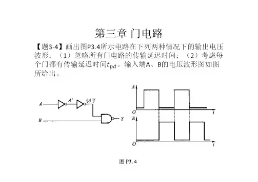
第三章门电路解:两种情况下的电压波形图如图A3.4所示。
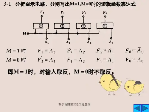
【题3.7】试分析图3.7中各电路图的逻辑功能,写出输出的逻辑函数式。
(a )图P3.7(a )电路可划分为四个反相器电路和一个三输入端的与非门电路,如图所示。
从输入到输出逐级写出输出的逻辑函数式,'111'1'1'1)(,,,C B A D C C B B A A ''''111')(C B A C B A C B A D Y(b )图P3.7(b )电路可划分为五个反相器电路和一个或非门电路,如图所示。
从输入到输出逐级写出输出的逻辑函数式:'111''''()()YA B C A B C ABC(c )图P3.7(c )电路可划分为三个与非门电路、两个反相器电路和一个或非门电路,如图所示。
从输入到输出逐级写出输出的逻辑函数式:''')(,)(,)'(,)(G INHH EF G CD F AB E '''''()()'()'()()Y I H AB CD INH AB CD INH(d)图P3.7(d)电路可划分为两个反相器电路和两个传输门电路,如图所示。
从输入到输出逐级写出输出的逻辑函数式:'YBAAB'【题3.8】试画出图3-8(a)(b)两个电路的输出电压波形,输入电压波形如图(c)所示。
输出电压波形如右图所示:【题3.9】 在图3-21所示电路中,G 1和G 2是两个OD 输出结构的与非门74HC03,74HC03输出端MOS 管截止电流为 导通时允许的最大负载电流为这时对应的输出电压V OL (max )=0.33V 。
负载门G 3-G 5是3输入端或非门74HC27,每个输入端的高电平输入电流最大值为 ,低电平输入电流最大值为 ,试求在 、、、、并且满足 ,的情况下, 的取值的允许范围。
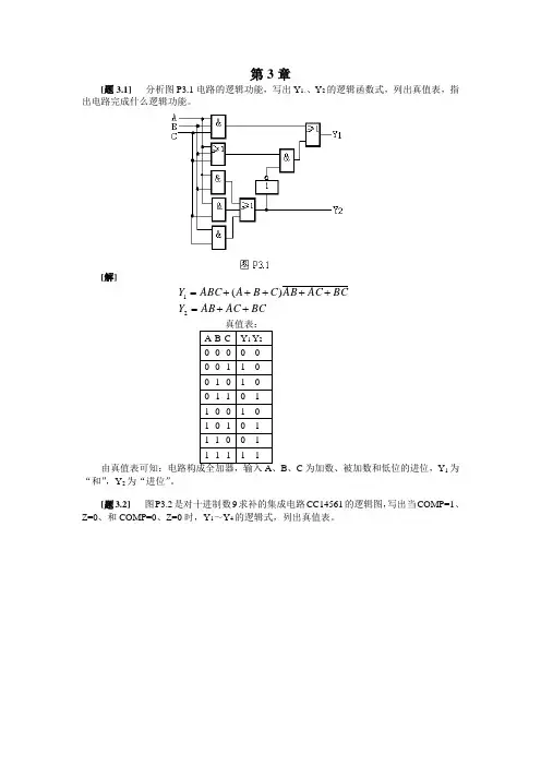
第3章[题3.1] 分析图P3.1电路的逻辑功能,写出Y 1、、Y 2的逻辑函数式,列出真值表,指出电路完成什么逻辑功能。
[解]BCAC AB Y BCAC AB C B A ABC Y ++=+++++=21)(B 、C 为加数、被加数和低位的进位,Y 1为“和”,Y 2为“进位”。
[题3.2] 图P3.2是对十进制数9求补的集成电路CC14561的逻辑图,写出当COMP=1、Z=0、和COMP=0、Z=0时,Y 1~Y 4的逻辑式,列出真值表。
[解](1)COMP=1、Z=0时,TG 1、TG 3、TG 5导通,TG 2、TG 4、TG 6关断。
3232211 , ,A A Y A Y A Y ⊕===, 4324A A A Y ++=(2)COMP=0、Z=0时,Y 1=A 1, Y 2=A 2, Y 3=A 3, Y 4=A 4。
COMP =0、Z=0的真值表从略。
[题3.3] 用与非门设计四变量的多数表决电路。
当输入变量A 、B 、C 、D 有3个或3个以上为1时输出为1,输入为其他状态时输出为0。
[解] 题3.3的真值表如表A3.3所示,逻辑图如图A3.3所示。
ABCD D ABC D C AB CD B A BCD A Y ++++= BCD ACD ABC ABC +++=B C D A C D A B D A B C ⋅⋅⋅=[题3.4] 有一水箱由大、小两台泵M L 和M S 供水,如图P3.4所示。
水箱中设置了3个水位检测元件A 、B 、C 。
水面低于检测元件时,检测元件给出高电平;水面高于检测元件时,检测元件给出低电平。
现要求当水位超过C 点时水泵停止工作;水位低于C 点而高于B 点时M S 单独工作;水位低于B 点而高于A 点时M L 单独工作;水位低于A 点时M L 和M S 同时工作。
试用门电路设计一个控制两台水泵的逻辑电路,要求电路尽量简单。
[解] 题3.4的真值表如表A3.4所示。
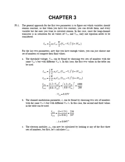
CHAPTER 3P3.1. The general approach for the first two parameters is to figure out which variables shouldremain constant, so that when you have two currents, you can divide them, and every variable but the ones you want to calculate remain. In this case, since the long-channel transistor is in saturation for all values of V GS and V DS , only one equation needs to be considered:()()2112DS N OX GS T DS W I C V V V Lμλ=-+ For the last two parameters, now that you have enough values, you can just choose oneset of numbers to compute their final values.a. The threshold voltage, V T0, can be found by choosing two sets of numbers with the same V DS ’s but with different V GS ’s. In this case, the first two values in the table can be used.()()()()()()211122222201022001121121.2 1.210000.82800.8DS N OX GS T DS DS N OX GS T DS T DS T DS T T W I C V V V L W I C V V V LV I V I V V μλμλ=-+=-+-⎛⎫-===⎪--⎝⎭ 00.35V T V ∴=b. The channel modulation parameter, λ, can be found by choosing two sets of numberswith the same V GS ’s but with different V DS ’s. In this case, the second and third values in the table can be used.()()221 1.225010.8247DS DS I I λλ+==+ -10.04V λ∴=c. The electron mobility, µn , can now be calculated by looking at any of the first three sets of numbers, but first, let’s calculate C OX .631062-31m 10μm22?.210μm1m 10 0.0351 1.610/2.210OX OX t C F cm--=⨯⨯===⨯Now calculate the mobility by using the first set of numbers.()()()()()()()()()()()()22111021262101111 1.21 1.222210002cm 348V-s 1.610(4.75)1.20.3510.04 1.21DS N OX GS T DS N OX T DS N OX GS T DS W W I C V V V C V L LA I W C V V V L μλμλμμλ-=-+=-+===⨯-+-+d. The body effect coefficient gamma, γ, can be calculated by using the last set of numbers since it is the only one that has a V SB greater than 0V.()()()()244124414411221 1.20.468VDS N OX GS T DS DS GS T N OX DS GS T T GS W I C V V V LI V V W C V LV V V V μλμλ=-+-=+-==-==12000.6VT T T T V V V V γγγ=+-====P3.2. The key to this question is to identify the transistor’s region of operation so that gatecapacitance may be assigned appropriately, and the primary capacitor that will dischargedat a rate of V It C ∂∂= by the current source may be identified. Then, because the nodes arechanging, the next region of operation must be identified. This process continues until the transistor reaches steady state behavior. Region 1:Since 0V GS V = the transistor is in the cutoff region. The gate capacitance is allocated to GB C . Since no current will flow through the transistor, all current will come from the source capacitor and the drain node remains unchanged.68-151010V V 6.67100.6671510s nsSB V I I t C C -∆⨯====⨯=∆⨯ The source capacitor will discharge until 1.1V GS T V V == when the transistor enters thesaturation region. This would require that the source node would be at 3.3 1.1 2.2V S G GS V V V =-=-=.()15961510 3.3 2.2 1.6510s 1.65ns 1010C t V I ---⨯∆=∆=-=⨯=⨯ Region 2:The transistor turns on and is in saturation. The current is provided from the capacitor atthe drain node, while the source node remains fairly constant. The capacitance at the drain node is the same as the source node so the rate of change is given by:68-151010V V 6.67100.6671510s nsSB V I I t C C -∆⨯====⨯=∆⨯ Since the transistor is now in the saturation region, GS V can be computed based on thecurrent flowing through the device.()22 1.1 1.37V 3.3 1.37 1.93VGS T GST S G GS kW I V V LV V V V V =-==+==-=-=This is where the source node settles. This means that most of the current is discharged through the transistor until the drain voltage reaches a value that puts the transistor at the edge of saturation.3.3 1.1 2.2VDS GS TD G T V V V V V V =-=-=-=If we assume that all the current comes from the transistor, and the source node remains fixed, the drain node will then discharge at a rate equal to that of the source node in the first region. Region 3:The transistor is now in the linear region the gate capacitance is distributed equally to both GS C and GD C . and both capacitors will discharge at approximately the same rate.-151510V0.28621510510nsV I A t C μ-∆===∆⨯⨯+⨯The graph is shown below.00.511.522.533.5024681012Time (ns)V o l t a g e (V )P3.3. The gate and drain are connected together so that DS GS V V = which will cause thetransistor to remain in saturation. This is a dc measurement so capacitances are not required. Connect the bulk to ground and run SPICE. P3.4. Run SPICE. P3.5. Run SPICE. P3.6. Run SPICE. P3.7. Run SPICE.P3.8. First, let’s look at the various parameters and identify how they affect V T .∙ L – Shorter lengths result in a lower threshold voltage due to DIBL. ∙ W – Narrow width can increase the threshold voltage.∙ V SB – Larger source-bulk voltages (in magnitude) result in a higher threshold voltage. ∙ V DS –Larger drain-source voltages (in magnitude) result in a lower threshold voltage due to DIBL. The transistor with the lowest threshold voltage has the shortest channel, larger width, smallest source-bulk voltage and largest drain-source voltage. This would be the first transistor listed.The transistor with the highest threshold voltage has the longest channel, smallest width,largest source-bulk voltage and smallest drain-source voltage. This would be the last transistor listed. P3.9. Run SPICE.P3.10. Run SPICE. The mobility degradation at high temperatures reduces I on and the increasemobile carriers at high temperatures increase I off . P3.11. The issues that prompted the switch from Al to Cu are resistance and electromigration.Copper wires have lower resistances and are less susceptible to electromigration problems. Copper on the other hand, reacts with the oxygen in SiO 2 and requires cladding around the wires to prevent this reaction.For low-k dielectrics, the target value future technologies is 2.High-k dielectrics are being developed as the gate-insulator material of MOSFET’s. This is because the current insulator material, SiO 2, can not be scaled any longer due to tunneling effects.P3.12. Self-aligned poly gates are fabricated by depositing oxide and poly before the source anddrain regions are implanted. Self-aligned silicides (salicides) are deposited on top of the source and drain regions using the spacers on the sides of the poly gate. P3.13. To compute the length, simply use the wire resistance equation and solve for L .LR TWRTWL ρρ==First convert the units of ρ to terms of μm. Aluminum:2.7μΩρ=cm 6Ω10μΩ⨯610μm100cm ⨯()()()0.027Ωμm1000.812963μm 2.96mm0.027RTWL ρ=====Copper:1.7μΩρ=cm 6Ω10μΩ⨯610μm100cm ⨯()()()0.017Ωμm1000.814706μm 4.71mm0.017RTWL ρ=====P3.14. Generally, the capacitance equation in terms of permittivity constants and spacing is:k C WL tε=a. 4k = ()()()()230048.8510 3.541100SiO k k C WL TL t S S Sεε-====b. 2k = ()()()()30028.8510 1.771100k k C WL TL t S SSεε-====The plots are shown below.Capacitance vs. Spacing01234567800.511.522.533.544.555.5Spacing (um)C a p a c i t a n c e (f F)。
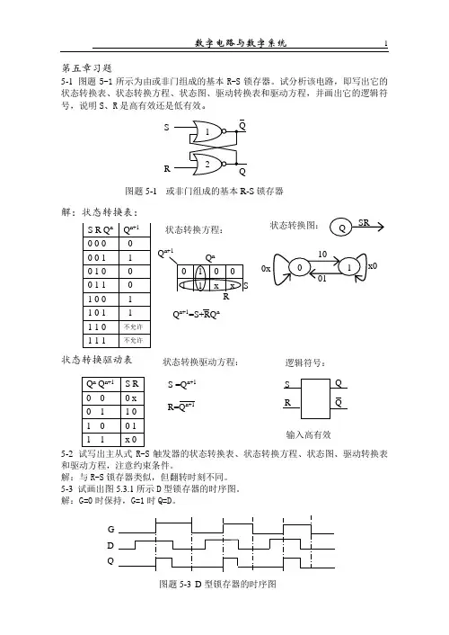
第三章锁存器与触发器一、选择题1.N个触发器可以构成能寄存位二进制数码的寄存器。
A.N-1B.NC.N+1D.2N2.一个触发器可记录一位二进制代码,它有个稳态。
A.0B.1C.2D.33.对于D触发器,欲使Q n+1=Q n,应使输入D= 。
A.0B.1C.QD.Q4.存储8位二进制信息要个触发器。
A.2B.3C.4D.85.对于T触发器,若原态Q n=0,欲使新态Q n+1=1,应使输入T= 。
A.0B.1C.QD.Q6.对于T触发器,若原态Q n=1,欲使新态Q n+1=1,应使输入T= 。
A.0B.1C.QD.Q7.在下列触发器中,有约束条件的是。
A.主从JK F/FB.主从D F/FC.同步RS F/FD.边沿D F/F8.对于JK触发器,若J=K,则可完成触发器的逻辑功能。
A.RSB.DC.TD.Tˊ9.欲使JK触发器按Q n+1=Q n工作,可使JK触发器的输入端。
A.J=K=0B.J=Q,K=QC.J=Q,K=QD.J=Q,K=0E.J=0,K=Q10.欲使JK触发器按Q n+1=Q n工作,可使JK触发器的输入端。
A.J=K=1B.J=Q,K=QC.J=Q,K=QD.J=Q,K=1E.J=1,K=Q11.欲使JK触发器按Q n+1=0工作,可使JK触发器的输入端。
A.J=K=1B.J=Q,K=QC.J=Q,K=1D.J=0,K=1E.J=K=112.欲使JK触发器按Q n+1=1工作,可使JK触发器的输入端。
A.J=K=1B.J=1,K=0C.J=K=QD.J=K=0E.J=Q,K=0 13.欲使D触发器按Q n+1=Q n工作,应使输入D= 。
A.0B.1C.QD.Q14.下列触发器中,克服了空翻现象的有。
A.边沿D触发器B.主从RS触发器C.同步RS触发器D.主从JK触发器15.下列触发器中,没有约束条件的是。
A.基本RS触发器B.主从RS触发器C.同步RS触发器D.边沿D触发器16.为实现将JK触发器转换为D触发器,应使。
第三章3.1 解:由图可写出Y 1、Y 2的逻辑表达式:BCAC AB Y C B A C B A C B A ABC BC AC AB C B A ABC Y ++=+++=+++++=21)(真值表:3.2 解:AY A Y A Y A Y Z comp A A A Y A A A A Y A Y A Y Z comp ======++=+=====43322114324323232210001,,,时,、,,,时,、, 真值表:3.3解:3.4解:采用正逻辑,低电平=0,高电平=1。
设水泵工作为1,不工作为0,由题目知,水泵工作情况只 有四种:全不工作,全工作,只有一个工作真值表:图略3.5 解:设输入由高位到低位依次为:A 4、A 3、A 2、A 1, 输出由高位到地位依次为:B 4、B 3、B 2、B 13.6 1111100000310对应编码为:,对应编码为:A A3.7解:此问题为一优先编码问题,74LS148为8-3优先编码器,只用四个输入端即可,这里用的是7~4,低4位不管;也可用低4位,但高位必须接1(代表无输入信号);用高4位时,低4位也可接1,以免无病房按时灯会亮。
3.8(图略)3.9 解: 3.11解:3.10解:3.12解:3.13解:3.14 由表知,当DIS=INH=0时DBCACDBACDBACB ADCBADCBAZCBADAAADAAADAAADAAADAAADAAADAAADAAAY+++++=+ ++++++=得:、、代入712612512412312212112123.15 PQNMPQNMQPMNQPNMZ+++=3.16 解:4选1逻辑式为:,,,,,,,,,,,的表达式,知:对比110104512)(1)(1)()(1)()(76543210012===========+++++=D D D D D D D D D D D C A B A A A DC B A ABC BC AD C B A C AB D C B A Y(3.17图)(3.18图)3.18解:方法同上题,只是函数为三变量,D 只取0或1即可,,,,,,,,,则有:,,取1010011076543210012===========D D D D D D D D C A B A A A3.19 解:设A 、B 、C 为三个开关,每个有两种状态0、1,若三个全为0则灯灭Y=0;否则,Y =1分析:全为0时灯灭;任何一个为1,则灯亮。
第三章集成逻辑门电路一、选择题1、三态门输出高阻状态时,( )就是正确的说法。
A、用电压表测量指针不动B、相当于悬空C、电压不高不低D、测量电阻指针不动2、以下电路中可以实现“线与”功能的有( )。
A、与非门B、三态输出门C、集电极开路门D、漏极开路门3.以下电路中常用于总线应用的有( )。
A、TSL门B、OC门C、漏极开路门D、CMOS与非门4.逻辑表达式Y=AB可以用( )实现。
A、正或门B、正非门C、正与门D、负或门5.TTL电路在正逻辑系统中,以下各种输入中( )相当于输入逻辑“1”。
A、悬空B、通过电阻2、7kΩ接电源C、通过电阻2、7kΩ接地D、通过电阻510Ω接地6.对于TTL与非门闲置输入端的处理,可以( )。
A、接电源B、通过电阻3kΩ接电源C、接地D、与有用输入端并联7.要使TTL与非门工作在转折区,可使输入端对地外接电阻RI( )。
A、>RONB、<ROFFC、ROFF<RI<ROND、>ROFF8.三极管作为开关使用时,要提高开关速度,可( )。
A、降低饱与深度B、增加饱与深度C、采用有源泄放回路D、采用抗饱与三极管9.CMOS数字集成电路与TTL数字集成电路相比突出的优点就是( )。
A、微功耗B、高速度C、高抗干扰能力D、电源范围宽10.与CT4000系列相对应的国际通用标准型号为( )。
A、CT74S肖特基系列B、 CT74LS低功耗肖特基系列C、CT74L低功耗系列D、 CT74H高速系列11.电路如图(a),(b)所示,设开关闭合为1、断开为0;灯亮为1、灯灭为0。
F 对开关A、B、C的逻辑函数表达式( )。
F1F 2(a)(b)A.C AB F =1 )(2B A C F +=B.C AB F =1 )(2B A C F +=C. C B A F =2 )(2B A C F +=12.某TTL 反相器的主要参数为IIH =20μA;IIL =1、4mA;IOH =400μA;水IOL =14mA,带同样的门数( )。
习题参考答案注:参考答案,并不是唯一答案或不一定是最好答案。
仅供大家参考。
第一章习题2. C B A D B A C B A F ⋅⋅+⋅⋅+⋅⋅=3. 设:逻辑变量A 、B 、C 、D 分别表示占有40%、30%、20%、10%股份的四个股东,各变量取值为1表示该股东投赞成票;F 表示表决结果,F =1表示表决通过。
F =AB +AC +BCD4. 设:A 、B 开关接至上方为1,接至下方为0;F 灯亮为1,灯灭为0。
F =A ⊙B5. 设:10kW 、15kW 、25kW 三台用电设备分别为A 、B 、C ,设15kW 和25kW 两台发电机组分别为Y 和Z ,且均用“0”表示不工作,用“1”表示工作。
C AB Z BA B A Y ⋅=⋅=6.输入为余3码,用A 、B 、C 、D 表示,输出为8421BCD 码,用Y 0、Y 1、Y 2、Y 3表示。
D C A B A Y CB DC BD B Y DC Y DY ⋅⋅+⋅=⋅+⋅⋅+⋅=⊕==32107. 设:红、绿、黄灯分别用A 、B 、C 表示,灯亮时为1,灯灭时为0;输出用F 表示,灯正常工作时为0,灯出现故障时为1。
C A B A C B A F ⋅+⋅+⋅⋅=8. D C B D A H DC B AD C B A D C B A D C B A G DC B AD C A B A F DC B A E ⋅⋅+⋅=⋅⋅⋅+⋅⋅⋅+⋅⋅⋅+⋅⋅⋅=⋅⋅⋅+⋅⋅+⋅=⋅⋅⋅=第二章习题1. 设:红、绿、黄灯分别用A 、B 、C 表示,灯亮时其值为1,灯灭时其值为0;输出报警信号用Y 表示,灯正常工作时其值为0,灯出现故障时其值为1。
AC AB C B A Y ⋅⋅=2. 设:烟、温度和有害气体三种不同类型的探测器的输出信号用A 、B 、C 表示,作为报警信号电路的输入,有火灾探测信号时用1表示,没有时用0表示。
报警信号电路的书躇用Y 表示,有报警信号时用1表示,没有时用0表示。
《数字电子技术基础》课后习题答案《数字电路与逻辑设计》作业教材:《数字电子技术基础》(高等教育出版社,第2版,2012年第7次印刷)第一章:自测题:一、1、小规模集成电路,中规模集成电路,大规模集成电路,超大规模集成电路5、各位权系数之和,1799、01100101,01100101,01100110;11100101,10011010,10011011二、1、×8、√10、×三、1、A4、B练习题:1.3、解:(1) 十六进制转二进制: 4 5 C0100 0101 1100二进制转八进制:010 001 011 1002 13 4十六进制转十进制:(45C)16=4*162+5*161+12*160=(1116)10所以:(45C)16=(10001011100)2=(2134)8=(1116)10(2) 十六进制转二进制: 6 D E . C 80110 1101 1110 . 1100 1000二进制转八进制:011 011 011 110 . 110 010 0003 3 3 6 . 6 2十六进制转十进制:(6DE.C8)16=6*162+13*161+14*160+13*16-1+8*16-2=(1 758.78125)10所以:(6DE.C8)16=(011011011110. 11001000)2=(3336.62)8=(1758.78125)10(3) 十六进制转二进制:8 F E . F D1000 1111 1110. 1111 1101二进制转八进制:100 011 111 110 . 111111 0104 3 7 6 . 7 7 2十六进制转十进制:(8FE.FD)16=8*162+15*161+14*160+15*16-1+13*1 6-2=(2302.98828125)10所以:(8FE.FD)16=(100011111110.11111101)2=(4376.772)8=(2302.98828125)10(4) 十六进制转二进制:7 9 E . F D0111 1001 1110 . 1111 1101二进制转八进制:011 110 011 110 . 111 111 0103 6 3 6 . 7 7 2十六进制转十进制:(79E.FD)16=7*162+9*161+14*160+15*16-1+13*16 -2=(1950. 98828125)10所以:(8FE.FD)16=(011110011110.11111101)2=(3636.772)8=(1 950.98828125)101.5、解:(74)10 =(0111 0100)8421BCD=(1010 0111)余3BCD (45.36)10=(0100 0101.0011 0110)8421BCD=(0111 1000.0110 1001 )余3BCD(136.45)10=(0001 0011 0110.0100 0101)8421BCD=(0100 0110 1001.0111 1000 )余3BCD (374.51)10=(0011 0111 0100.0101 0001)8421BCD=(0110 1010 0111.1000 0100)余3BCD1.8、解(1)(+35)=(0 100011)原= (0 100011)补(2)(+56 )=(0 111000)原= (0 111000)补(3)(-26)=(1 11010)原= (1 11101)补(4)(-67)=(1 1000011)原= (1 1000110)补第二章:自测题:一、1、与运算、或运算、非运算3、代入规则、反演规则、对偶规则二、2、×4、×三、1、B3、D5、C练习题:2.2:(4)解:Y=AB̅+BD+DCE+A̅D=AB̅+BD+AD+A̅D+DCE=AB̅+BD+D+DCE=AB̅+D (B +1+CE ) =AB̅+D (8)解:Y =(A ̅+B ̅+C ̅)(D ̅+E ̅)̅̅̅̅̅̅̅̅̅̅̅̅̅̅̅̅̅̅̅̅̅̅̅̅̅̅(A ̅+B ̅+C ̅+DE ) =[(A ̅+B ̅+C ̅)̅̅̅̅̅̅̅̅̅̅̅̅̅̅̅̅+(D ̅+E ̅)̅̅̅̅̅̅̅̅̅̅](A ̅+B ̅+C ̅+DE ) =(ABC +DE )(ABC ̅̅̅̅̅̅+DE ) =DE 2.3:(2)证明:左边=A +A ̅(B +C)̅̅̅̅̅̅̅̅̅̅̅̅ =A +A ̅+(B +C)̅̅̅̅̅̅̅̅̅̅=A +B̅C ̅ =右式所以等式成立(4)证明:左边= (A̅B +AB ̅)⨁C = (A̅B +AB ̅)C ̅+ (A ̅B +AB ̅)̅̅̅̅̅̅̅̅̅̅̅̅̅̅̅C = (A ̅BC ̅+AB ̅C ̅)+A ̅B ̅̅̅̅⋅AB̅̅̅̅̅⋅C =A̅BC ̅+AB ̅C ̅+(A +B ̅)(A ̅+B )C =A̅BC ̅+AB ̅C ̅+(AB +A ̅B ̅)C =A̅BC ̅+AB ̅C ̅+ABC +A ̅B ̅C 右边= ABC +(A +B +C )AB ̅̅̅̅⋅BC ̅̅̅̅⋅CA̅̅̅̅ =ABC +(A +B +C )[(A̅+B ̅)(B ̅+C ̅)(C ̅+A ̅)] =ABC +(A +B +C )(A̅B ̅+A ̅C ̅+B ̅+B ̅C ̅)(C ̅+A ̅)=ABC +(A +B +C )(A̅B ̅C ̅+A ̅C ̅+B ̅C ̅+A ̅B ̅) =ABC +AB̅C ̅+A ̅BC ̅+A ̅B ̅C 左边=右边,所以等式成立 2.4(1)Y ′=(A +B ̅C ̅)(A ̅+BC) 2.5(3)Y ̅=A ̅B ̅(C ̅+D ̅)̅̅̅̅̅̅̅̅̅̅̅̅̅̅̅ C ̅D ̅(A ̅+B ̅)̅̅̅̅̅̅̅̅̅̅̅̅̅̅̅ 2.6:(1)Y =AB +AC +BC=AB (C +C̅)+AC (B +B ̅)+BC (A +A ̅) =ABC +ABC ̅+AB ̅C +A ̅BC 2.7:(1)Y =A ̅B ̅+B ̅C ̅+AC +B ̅C 卡诺图如下: B C A 00 0111100 1 1 1111所以,Y=B̅+AC2.8:(2)画卡诺图如下:B C A 0001 11 100 1 1 0 11 1 1 1 1Y(A,B,C)=A+B̅+C̅2.9:(1)画Y(A,B,C,D)=∑m(0,1,2,3,4,6,8)+∑d(10,11,12,13,14)如下:CDAB00 01 11 1000 1 1 1 101 1 111 ×××10 1 ××Y (A,B,C,D )=A̅B ̅+D ̅ 2.10:(3)解:化简最小项式: Y =AB +(A̅B +C ̅)(A ̅B ̅+C ) =AB +(A̅B A ̅B ̅+A ̅BC +A ̅B ̅C ̅+C ̅C ) =AB (C +C̅)+A ̅BC +A ̅B ̅C ̅ =ABC +ABC ̅+A ̅BC +A ̅B ̅C ̅ =∑m (0,3,6,7)最大项式:Y =∏M(1,2,4,5) 2.13:(3)Y =AB̅+BC ̅+AB ̅C ̅+ABC ̅D ̅ =AB̅(1+C ̅)+BC ̅(1+AD ̅) =AB̅+BC ̅ =AB̅+BC ̅̿̿̿̿̿̿̿̿̿̿̿̿ = AB̅̅̅̅̅∙BC ̅̅̅̅̅̅̅̅̅̅̅̅̅̅̅̅技能题:2.16 解:设三种不同火灾探测器分别为A 、B 、C ,有信号时值为1,无信号时为0,根据题意,画卡诺图如下:B C A 00 01 11 10 0 0 0 1 0 1 0 1 1 1Y =AB +AC +BC=AB +AC +BC ̿̿̿̿̿̿̿̿̿̿̿̿̿̿̿̿̿̿̿=AB ̅̅̅̅⋅AC ̅̅̅̅⋅BC ̅̅̅̅̅̅̅̅̅̅̅̅̅̅̅̅̅̅̅̅=(A ̅+B ̅)(A ̅+C ̅)(B ̅+C ̅)̅̅̅̅̅̅̅̅̅̅̅̅̅̅̅̅̅̅̅̅̅̅̅̅̅̅̅̅̅̅̅=A ̅+B ̅̅̅̅̅̅̅̅̅+A ̅+C ̅̅̅̅̅̅̅̅̅+B ̅+C ̅̅̅̅̅̅̅̅̅第三章:自测题:一、1、饱和,截止7、接高电平,和有用输入端并接,悬空;二、1、√8、√;三、1、A4、D练习题:3.2、解:(a)因为接地电阻4.7k Ω,开门电阻3k Ω,R>R on ,相当于接入高电平1,所以Y =A ̅B ̅1̅̅̅̅̅̅=A +B +0=A +B(e) 因为接地电阻510Ω,关门电0.8k Ω,R<R off ,相当于接入高电平0,所以、Y =A +B +0̅̅̅̅̅̅̅̅̅̅̅̅̅=A̅⋅B ̅∙1̅̅̅̅̅̅̅̅̅̅=A +B +0=A +B3.4、解:(a) Y1=A+B+0̅̅̅̅̅̅̅̅̅̅̅̅̅=A+B̅̅̅̅̅̅̅̅(c) Y3=A+B+1̅̅̅̅̅̅̅̅̅̅̅̅̅=1̅=0(f) Y6=A⋅0+B⋅1̅̅̅̅̅̅̅̅̅̅̅̅̅̅̅̅=B̅3.7、解:(a) Y1=A⨁B⋅C=(A̅B+AB̅)C=A̅BC+AB̅C3.8、解:输出高电平时,带负载的个数2020400===IHOHOH I I NG 可带20个同类反相器输出低电平时,带负载的个数78.1745.08===ILOLOL I I NG 反相器可带17个同类反相器3.12EN=1时,Y 1=A , Y 2=B ̅EN=0时,Y 1=A ̅, Y 2=B3.17根据题意,设A为具有否决权的股东,其余两位股东为B、C,画卡诺图如下,BCA00 01 11 100 0 0 0 01 0 1 1 1则表达结果Y的表达式为:Y=AB+AC=AB+AC̿̿̿̿̿̿̿̿̿̿̿̿=AB̅̅̅̅⋅AC̅̅̅̅̅̅̅̅̅̅̅̅̅̅逻辑电路如下:技能题:3.20:解:根据题意,A、B、C、D变量的卡诺图如下:CD AB00 01 11 1000 0 0 0 001 0 0 0 011 0 1 1 110 0 0 0 0Y =ABC +ABD =ABC +ABD ̿̿̿̿̿̿̿̿̿̿̿̿̿̿̿̿=ABC ̅̅̅̅̅̅⋅ABD ̅̅̅̅̅̅̅̅̅̅̅̅̅̅̅̅̅̅̅̅̅̅电路图如下:第四章:自测题:一、2、输入信号,优先级别最高的输入信号7、用以比较两组二进制数的大小或相等的电路,A>B 二、3、√4、√三、5、A7、C练习题:4.1;解:(a) Y =A⨁B +B ̅̅̅̅̅̅̅̅̅̅̅̅̅=A ̅B +AB ̅+B ̅̅̅̅̅̅̅̅̅̅̅̅̅̅̅̅̅̅̅=A ̅B +B ̅̅̅̅̅̅̅̅̅̅̅=A ̅+B̅̅̅̅̅̅̅̅̅=AB ,所以电路为与门。