PCB英文词汇
- 格式:xls
- 大小:67.50 KB
- 文档页数:24
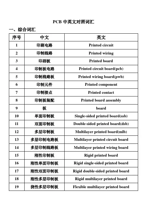
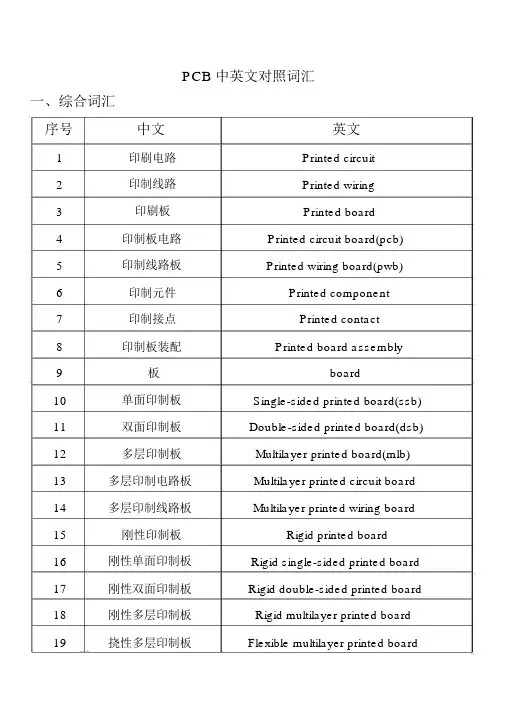
PCB 中英文对照词汇一、综合词汇序号中文英文1印刷电路Printed circuit2印制线路Printed wiring3印刷板Printed board4印制板电路Printed circuit board(pcb)5印制线路板Printed wiring board(pwb)6印制元件Printed component7印制接点Printed contact8印制板装配Printed board assembly9板board10单面印制板Single-sided printed board(ssb) 11双面印制板Double-sided printed board(dsb) 12多层印制板Multilayer printed board(mlb) 13多层印制电路板Multilayer printed circuit board 14多层印制线路板Multilayer printed wiring board 15刚性印制板Rigid printed board16刚性单面印制板Rigid single-sided printed board 17刚性双面印制板Rigid double-sided printed board 18刚性多层印制板Rigid multilayer printed board 19挠性多层印制板Flexible multilayer printed board20挠性印制板Flexible printed board21挠性单面印制板Flexible single-sided printed board22挠性双面印制板Flexible double-sided printed board23挠性印制电路Flexible printed circuit(fpc)24挠性印制线路Flexible printed wiring25刚性印制线路Flex-rigid printed board 、 rigid-flexprinted board26刚性双面印制板Flex-rigid double-sided printed board、rigid-flex double-sided printed27刚性多层印制板Flex-rigid multilayer printed board、rigid-flex double-sided printed28齐平印制板Flush printed board29金属芯印制板Metal core printed board30金属基印制板Metal base printed board31多重布线印制板Mulit-wiring printed board32陶瓷印制板Ceramic substrate printed board33导电胶印制板Electroconductive paste printed board34模塑电路板Molded circuit board35模压印制板Stamped printed wiring board36顺序层压多层印制板Sequentially-laminated multilayer37散线印制板Discrete wiring board38微线印制板Micro wire board39积层印制板Build-up printed board40积层多层印板Build-up multilayer printed board (bum) 41积层挠性印制板Build-up flexible printed board42表面层合电路板Surface laminar circuit(slc)43埋入凸块连印制板B2it printed board44多层膜基板Mutil-layered film substrate(mfs) 45层间全内导通多层印Alivh multiplayer printed board制板46载芯片板Chip on board (cob)47埋电阻板Buried resistance board48母板Mother board49子板Daughter board50背板backplane51裸板Bare board52键盘板夹心板Copper-invar-copper board53动态挠性板Dynamic flex board54静态挠性板Static flex board55可断拼板Break-away planel56电缆cable57挠性扁平电缆Flexible flat cable (ffc)58薄膜开关Membrance switch59混合开关Hybrid circuit60厚膜Thick film61厚膜电路Thick film circuit62薄膜Thin film63薄膜混合电路Thin film hybrid circuit 64互连interconnection65导线Conductor trace line 66齐平导线Flush conductor 67传输线Transmission line 68跨交crossover69板边插头Edge-board contact 70增强板stiffener71基底Substrate72基板面Real estate73导线面Conductor side74元件面Component side 75焊接面Solder side76印制Printing77网格Grid78图形Pattern79导电图形Conductive pattern 80非导电图形Non-conductive pattern 81字符legend82标志mark二、基材序号中文英文1基材Base material2层压板Laminate3覆金属箔基材Metal-clad bade material4覆铜箔层压板Copper-clad laminate(ccl)5单面覆铜箔层压板Single-sided copper-clad laminate 6双面覆铜箔层压板Double-sided copper laminate 7复合层压板Composite laminate8薄层压板Thin laminate9金属芯覆铜箔层压板Metal core copper-clad laminate 10金属基覆铜层压板Metal base copper-clad laminate 11挠性覆铜箔绝缘薄膜Flexible copper-clad dielectric film 12基体材料Basis material13预浸材料Prepreg14粘结片Bonding sheet15预浸粘结片Preimpregnated bonding sheet 16环氧玻璃基板Epoxy glass substrate17加成法用层压板Laminate for additive process 18预制内层覆箔板Mass laminate panel19内层芯板Core material20催化板材Catalyzed board21涂胶催化层压板Adhesive-coated catalyzed laminate 22涂胶无催化层压板Adhesive-coated uncatalyzed laminate 23粘结层Bonding layer24粘结膜Film adhesive25涂胶粘剂绝缘薄膜Adhesive coated dielectric film26无支撑胶粘剂膜Unsupported adhesive film27覆盖层Cover layer28增强板材Stiffener material29铜箔面Copper-clad surface30去铜箔面Foil removal surface31层压板面Unclad laminate surface32基膜面Base film surface33胶粘剂面Adhesive face34原始光洁面Plate finish35粗面Matt finish36纵向Length wise direction37横向Cross wise direction38剪切板Cut to size panel39酚醛纸质覆铜箔板Phenolic cellulose paper copper-cladlaminates(phenolic paper ccl)40环氧纸质覆铜箔板Epoxide cellulose paper copper-cladlaminates(epoxy paper ccl)41环氧玻璃布基覆铜箔Epoxide woven glass fabric copper-clad 板laminate42环氧玻璃布纸复合覆Epoxide cellulose paper core glass cloth 铜箔板surfaces copper-clad laminate43环氧玻璃布玻璃纤维Epoxide non woven glass reinforced 复合覆铜箔板copper-clad laminate44聚酯玻璃布覆铜箔板Polyester wovenglass fabric copper-clad laminate45聚酰亚胺玻璃布覆铜Polyimide woven glass fabric copper-clad箔板laminate46双马来酰亚胺三嗪环Bismaleimide triazine epoxide woven 氧玻璃布覆铜板glass fabric copper-clad laminate47环氧合成纤维布覆铜Epoxide synthetic fiber copper-clad箔板laminates48聚四乙烯玻璃纤维覆Teflon fiber glass copper-clad laminate铜箔板49超薄型层压板Ultra thin laminate50陶瓷基覆铜箔板Ceramincs base copper-clad laminate 51紫外线阻挡型覆铜箔Uv blocking copper-clad laminates板三、基材的材料序号中文英文1 a 阶树脂a-stage resin2 b 阶树脂b-stage resin3 c 阶树脂c-stage resin4环氧树脂Epoxy resin5酚醛树脂Phenolic resin6聚酯树脂Polyester resin7聚酰亚胺树脂Polyimide resin8双马来酰亚胺三嗪树Bismaleimide-triazine resin脂9丙烯酸树脂Acrylic resin10三聚氰胺甲醛树脂Melamine formaldehyde resin 11多功能环氧树脂Polyfunctional epoxy resin 12溴化环氧树脂Brominated epoxy resin 13环氧酚醛Epoxy novolac14氟树脂fluroresin15硅树脂Silicone resin16硅烷silane17聚合物polymer18无定形聚合物Amorphous polymer19结晶现象Crystalline polamer20双晶现象dimorphism21共聚物copolymer22合成树脂synthetic23热固性树脂Thermosetting resin24热塑性树脂Thermoplastic resin25感光性树脂Photosensitive resin26环氧当量Weight per epoxy equipvalent(wpe) 27环氧值Epoxy value28双氰胺dicyandiamide29粘结剂binder30固化剂Curing agent31胶粘剂adesive32阻燃剂Flame retardant33遮光剂opaquer34增塑剂plasticizers35不饱和聚酯Unsatuiated polyster36聚酯薄膜polyester37聚酰亚胺薄膜Polyimide film(pi)38聚四氟乙烯Polytetrafluoetylene(ptfe)39聚四氟乙烯丙烯薄膜Perfluorinated ethylene-propylenecopolymer film(fep)40增强材料Reinforcing material41玻璃纤维Glass fiber42 E 玻璃纤维e-glass fiber43 D 玻璃纤维d-glass fiber44S 玻璃纤维s-glass fiber45玻璃布Glass fabric46非织布Non-woven fabric 47玻璃纤维垫Glass mats48纱线yarn49单丝filament50胶股strand51纬纱Weft yarn52经纱Warp yarn53但尼尔denier54经向Warp-wise55纬向Weft-wise 、 filling-wise 56织物经纬密度Thread count57织物组织Weave structure58平纹组织Plain structure59坏布Grey fabric60稀松织物Woven scrim61弓纬Bow of weave62断经End missing63缺纬Mis-picks64纬斜bias65折痕crease66云织waviness67鱼眼Fish eye68毛圈长Feather length69厚薄段mark70裂缝spilt71捻度Twist of yarn72浸润剂含量Size content73浸润剂残留量Size residue74处理剂含量Finish leval75浸润剂size76偶联剂Couplint agent77处理织物Finished fabric78聚酰胺纤维Polyarmide fiber79聚酯纤维非织布Non-woven polyester fabric 80浸渍绝缘纵纸Impregenating insulation paper 81聚芳酰胺纤维纸Aromatic polyamide paper 82断裂长Breaking length83吸水高度Height of capillary rise84湿强度保留率Wet strength retention85白度whitenness86陶瓷ceramics87导电箔Conductive foil88铜箔Copper foil89电解铜箔Electrodeposited copper foil (ed copperfoil)90压延铜箔Rolled copper foil91退火铜箔Annealed copper foil92压延退火铜箔Rolled annealed copper foil (ra copperfoil)93薄铜箔Thin copper foil94涂胶铜箔Adhesive coated foil95涂胶脂铜箔Resin coated copper foil(rcc)96复合金属箔Composite metallic material97载体搏Carrier foil98殷瓦invar99箔(剖面)轮廓Foil profile100光面Shiny side101粗糙面Matte side102处理面Treated side103防锈处理Stain proofing104双面处理铜箔Double treated foil四、设计序号中文英文1原理图Shematic diagram2逻辑图Logic diagram3印制线路布设Printed wire layout4布设总图Master drawing5可制造性设计Design-for-manufacturability6计算机辅助设计Computer-aided design(cad)7计算机辅助制造Computer-aided manufacturability(cim) 8计算机集成制造Computer integrat manufacturing 9计算机辅助工程Computer-aided engineering(cae) 10计算机辅助测试Computer-aided test (cat)11电子设计自动化Electric design automaton(eda) 12工程设计自动化Engineering design automaton(eda2) 13组装设计自动化Assemnly aided architecturaldesign(aaad) 14计算机辅助制图Computer aided drawing15计算机控制显示Computer controlled display(ccd) 16布局placement17布线routing18布图设计layout19重布rerouting20模拟simulation21逻辑模拟Logic simulation22电路模拟Circit simulate23时序模拟Timing simulation24模块化modularization25布线完成率Layout effeciency26机器描述格式Machine descriptionm format(mdf) 27机器描述格式数据库Mdf database28设计数据库Design database29设计原点Design origin30优化(设计)Optimization(design)31供设计优化坐标轴Predominant axis32表格原点Table origin33镜像Mirroring34驱动文件Drive file35中间文件Intermediate file36制造文件Manufacturing documentation 37队列支撑数据库Queue support database38元件安置component positioning 39图形显示Graphics display40比例因子Scaling factor41扫描填充Scan filling42矩形填充Rectangle filling43填充域Region filling44实体设计Physical design45逻辑设计Logic design46逻辑电路Logic design47层次设计Hierarchical design48自顶向下设计Top-down design49自顶向上设计Bottom-up design50线网net51数字化digitzing52设计规则检查Design rule checking53走(布)线路Router(cad)54网络表Net list55计算机辅助电路分析Computer-aided circuit analysis 56子线网Subnet57目标函数Objective function58设计后处理Post design processing(pdp) 59交互式制图设计Interactive drawing design 60费用矩阵Cost metrix61工程图Engineering drawing62方块框图Block diagram63迷宫Moze64元件密度Component density65巡回售货员问题Traveling salesman problem 66自由度Degrees freedom67入度Out going degree68出度Incoming degree69曼哈顿距离Manhatton distance70欧几里德距离Euclidean distance71网络Network72阵列Array73段Segment74逻辑Logic75逻辑设计自动化Logic design automation 76分线Separated time77分层Separated layer78定顺序Definite sequence79对准度registration80孔环Annular ring81公差Tolerance82同心Concentricity83样片coupon84变色discolorations85污点Stains86试样Specimen 87钻孔Drilling88剪裁Shearing 89切外型Routing90刮线Scoring91倒角Chamfering 92切空Blanking 93适应性suitability 94板弯Bow95板扭Twist96应力Stress97防焊膜Solder mask 98阻焊膜Solder resist 99文字标记Legend 100版本代字Revision letter 101料号Part No 102跳漏Skipping 103浮空Soda strawing 104流动Flow 105整平Leveling 106FPR First pass yield ‘。
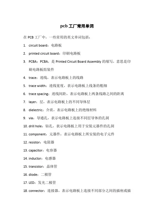
pcb工厂常用单词
在PCB工厂中,一些常用的英文单词包括:
1.circuit board:电路板
2.printed circuit board:印刷电路板
3.PCBA:PCBA,是Printed Circuit Board Assembly的缩写,意思是印
刷电路板组装件
4.trace:迹线,表示电路板上的线路
5.trace width:迹线宽度,表示电路板上线条的粗细
6.trace spacing:迹线间距,表示电路板上两条线路之间的距离
yer:层,表示电路板上的不同导体层
8.dielectric:介质,表示电路板上的绝缘材料
9.via:导通孔,表示电路板上连接不同层导体的孔洞
10.drill hole:钻孔,表示电路板上用于安装元器件的孔洞
ponent:元器件,表示电路板上所安装的电子元件
12.resistor:电阻器
13.capacitor:电容器
14.inductor:电感器
15.transistor:晶体管
16.diode:二极管
17.LED:发光二极管
18.connector:连接器,表示电路板上连接不同部分之间的插座或插
头
19.jumper:跳线,表示用于连接不同部分的短导线
20.tooling hole:工具孔,表示电路板上用于安装治具的孔洞
21.mounting hole:安装孔,表示电路板上用于安装元器件的孔洞
以上仅是部分常用词汇,实际工作中还会涉及到更多专业术语和词汇。
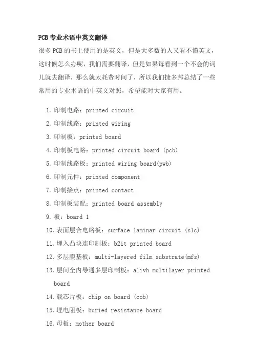
PCB专业术语中英文翻译很多PCB的书上使用的是英文,但是大多数的人又看不懂英文,这时候怎么办呢,我们需要翻译,但是如果每看到一个不会的词儿就去翻译,那么就太耗费时间了,所以我们捷多邦总结了一些常用的专业术语的中英文对照,希望能对大家有用。
1.印制电路:printed circuit2.印制线路:printed wiring3.印制板:printed board4.印制板电路:printed circuit board (pcb)5.印制线路板:printed wiring board(pwb)6.印制元件:printed component7.印制接点:printed contact8.印制板装配:printed board assembly9.板:board 110.表面层合电路板:surface laminar circuit (slc)11.埋入凸块连印制板:b2it printed board12.多层膜基板:multi-layered film substrate(mfs)13.层间全内导通多层印制板:alivh multilayer printed board14.载芯片板:chip on board (cob)15.埋电阻板:buried resistance board16.母板:mother board17.单面印制板:single-sided printed board(ssb)18.双面印制板:double-sided printed board(dsb)19.多层印制板:mulitlayer printed board(mlb)20.多层印制电路板:mulitlayer printed circuit board21.多层印制线路板:mulitlayer prited wiring board22.刚性印制板:rigid printed board23.刚性单面印制板:rigid single-sided printed borad24.刚性双面印制板:rigid double-sided printed borad25.刚性多层印制板:rigid multilayer printed board26.子板:daughter board27.背板:backplane28.裸板:bare board29.键盘板夹心板:copper-invar-copper board30.动态挠性板:dynamic flex board31.静态挠性板:static flex board32.可断拼板:break-away planel33.电缆:cable34.挠性扁平电缆:flexible flat cable (ffc)35.薄膜开关:membrane switch36.混合电路:hybrid circuit37.厚膜:thick film38.厚膜电路:thick film circuit39.薄膜:thin film40.挠性多层印制板:flexible multilayer printed board41.挠性印制板:flexible printed board42.挠性单面印制板:flexible single-sided printed board43.挠性双面印制板:flexible double-sided printed board44.挠性印制电路:flexible printed circuit (fpc)45.挠性印制线路:flexible printed wiring46.刚性印制板:flex-rigid printed board, rigid-flex printedboard47.刚性双面印制板:flex-rigid double-sided printed board,rigid-flex double-sided printed48.刚性多层印制板:flex-rigid multilayer printed board,rigid-flex multilayer printed board49.齐平印制板:flush printed board50.金属芯印制板:metal core printed board51.金属基印制板:metal base printed board52.多重布线印制板:mulit-wiring printed board53.陶瓷印制板:ceramic substrate printed board54.导电胶印制板:electroconductive paste printed board55.模塑电路板:molded circuit board56.模压印制板:stamped printed wiring board57.顺序层压多层印制板:sequentially-laminated mulitlayer58.散线印制板:discrete wiring board59.微线印制板:micro wire board60.积层印制板:buile-up printed board61.积层多层印制板:build-up mulitlayer printed board (bum)62.积层挠印制板:build-up flexible pr上面是一些比较常见的专业用语,有一些不是特别常用的有时候我们也会遇到,所以我们捷多邦也总结了一些不怎么常用的中英文对照,希望对你来说是有用的:1.Absorption 吸收、吸入2.Accelerated Test(Aging)加速试验、加速老化3.Accelerator 加速剂、速化剂4.Accept/Acceptance 允收5.Acceptable Quality Level(AQL)允收品质水准6.Accuracy 准确度ACF:7.Adhesive copper foil 有胶铜箔8.Activator 活化剂、添加剂比称为9.Activator Active parts(Devices)主动零件,指积体电路或电晶体10.Addition Agent 添加剂11.Additive Process 加成法、分全加成、半加成及部份加成12.Back Light(Back Lighting)背光法13.Back-UP 垫板14.Backpanels/ Backplanes 背板、支持板,厚度较厚,15.Ball Grid Array(BGA)球脚车列(封装)16.Barrel 孔壁17.Base Material 基材18.Batch 批(同时间发料某一数量的板子)19.Bevelling 切斜边20.Binder 黏结剂21.Capacitance 电容22.Carbide 碳化物、碳化钨钻头23.CAR: Corrective Action Report 改善报告24.Carbon Treatment 活性碳处理25.Card 卡板26.Carrier 载体27.Cartridge 滤芯28.Cathode 阴极L: Copper Clad Laminates 铜箔基板30.Ceramics 陶瓷31.Certificate 证明书32.CFC 氟氯碳化物33.Chloro-Fluoro-Carbon Chamfer 倒角、去掉直角34.Characteristic Impedance 特性阻抗35.Cheek list 检察清单36.Chip 晶粒、晶片37.Chip On Board 晶片黏著板38.Clean Room 无尘室(Class 100)39.Cleanliness 清洁度40.Clearance 余隙、余环41.COB(Chip on Board)晶片在板上直接组装42.COC(Certificate of Compliance)出货合格书。
PCB专业英译术语PCB(Printed Circuit Board,印刷电路板)是现代电子产品中最常用的一种重要的电路载体,其设计、生产和维修需要大量的技术术语支持。
本文将重点介绍PCB专业英译术语。
一、PCB基础术语1. PCB(Printed Circuit Board):印刷电路板2. SMT(Surface Mount Technology):表面贴装技术3. Through-hole Technology:通孔技术4. PTH(Plated Through Hole):贯穿电解孔5. FR4:一种常用的印刷电路板基材材料,即玻璃纤维材料,通常由环氧树脂和玻璃纤维材料构成6. Pad:焊盘7. Trace:线路8. Via:垂直插孔9. Gerber file:Gerber文件格式,一种电路板设计文件格式10. BOM(Bill of Materials):物料清单11. NC(Numerical Control):数控12. DFM(Design for Manufacturability):可制造性设计二、PCB制造过程相关术语1. CAM(Computer Aided Manufacturing):计算机辅助制造2. Etch:蚀刻3. Silkscreen:丝网印刷4. Solder mask:焊盘油墨5. Plating:电镀6. HASL(Hot Air Solder Leveling):热风焊盘处理7. OSP(Organic Solderability Preservatives):有机可焊保护剂8. Gold Fingers:金手指,指电子产品中可进行插拔操作的特殊金属触点9. DIP(Dual In-line Package):双列直插封装10. SOP(Small Outline Package):小封装11. QFN(Quad Flat Package):四角平封12. BGA(Ball Grid Array):球网阵列13. PCBA(Printed Circuit Board Assembly):印刷电路板装配三、PCB测试和维修相关术语1. AOI(Automated Optical Inspection):自动光学检测2. X-ray Inspection:X光检测3. ICT(In-Circuit Test):在线测试4. FCT(Functional Circuit Test):功能测试5. Test point:测试点6. Defect:缺陷7. Repair:修复8. Rework:返工9. Troubleshooting:故障排除四、PCB设计相关术语1. EDA(Electronic Design Automation):电子设计自动化2. Netlist:网表3. DRC(Design Rule Check):设计规则检查4. DFM(Design for Manufacturing):可制造性设计5. Gerber data:Gerber数据6. Simulation:仿真7. Library:元件库8. Footprint:封装9. Copper pour:铜质填充10. Via tenting:垂直插孔塞堵11. Blind vias:盲孔12. Buried vias:穿过孔五、总结本文介绍了PCB专业英译术语中的基础术语、PCB制造过程相关术语、PCB测试和维修相关术语以及PCB设计相关术语。
PCB 工程部专业英文词汇词汇1.板料: material2.最低限度: minimum 或者min.3.最大限度:maximum 或者max。
4.基准点(零点) datum point5.周期Date code6.V—cut余厚V-cut remain thickness7.抢电铜皮(假铜)dummy copper8.实物板actual board9.外形及尺寸错误dimension error10.异常情形error data file11.焊锡面与零件面对位偏差misregistration12.孔塞plug hole13.要求requirement14.缺少miss15.偏公差uneven tolerance16.补偿compensation17.表面处理surface treatment18.无铅喷锡Lead free HAL19.金手指斜边bevel of G/F20.制程能力process capability21.建议,暗示suggest22.确保ensure23.满足,达到meet24.为了in order to25.交货期delivery date26.绿油桥solder mask bridge 或者solder mask dam27.根据according to28.单边3mil per side 3 mil29.直径diameter30.半径radius 31.小于3mil less than 3mil32.高于3mil more than 3 mil33.压合结构stacking structure 或者stack_up34.附件:attached file35.样品:sample36.文档:Document37.答复:answer; reply38.规格:spec39.与.。
同样的:the same as40.前版本:previous version(old version)41.生产:production42.确认:confirm43.再次确认:confirm again44.工程问题:engineering query(EQ)45.尽快:as soon as possible46.生产文件:production Gerber47.联系某人:contact somebody48.提交样板:submit sample49.交货期:delivery date50.电测成本:ET(electrical test)cost51.通断测试:Open and short testing52.参考:refer to53.IPC标准:IPC standard54.IPC二级:IPC class 255.可接受的:acceptable56.允许:permit57.制造:manufacture 或者fabricate58.修改:revision59.公差:tolerance60.忽略:ignore61.工具孔:tooling hole62.安装孔:mounting hole63.元件孔:component hole64.槽孔:slot hole65.邮票孔:snap off hole 或者stamp hole66.导通孔:via hole67.盲孔:blind via hole68.埋孔:buried via hole69.金属化孔:PTH(plated through hole)70.非金属化孔:NPTH(no plated through hole)71.孔位:hole location72.避免:avoid73.原设计:original design74.修改:modify75.按原设计:follow up original design76.附边:waste tab,waste area 或者breakaway tab77.铜条:copper strip78.拼板:panel drawing79.板厚:board thickness80.删除:remove(delete)81.削铜:shave the copper82.露铜:copper exposure 或者exposed copper83.光标点:fiducial mark84.不同:be different from(differ from)85.内弧:inside radius86.焊环:annular ring87.单板尺寸:single size88.拼板尺寸:panel size89.铣,锣:routing90.铣刀:router 或者Routing bit91.楔形掏槽V—cut 或者V scoring92.哑光:matt93.光亮的:glossy94.锡珠:solder ball(solder plugs)95.阻焊:solder mask(solder resist)96.阻焊开窗:solder mask opening 97.单面开窗:single side mask opening98.补油:touch up solder mask99.补线:track welds100.毛刺:burrs101.去毛刺:deburr102.镀层厚度:plating thickness103.清洁度:cleanliness104.离子污染:ionic contamination105.阻燃性等级:flammability retardant rating 106.黑化:black oxidation107.棕化:brown oxidation108.红化:red oxidation109.可焊性不良:poor solderability110.焊料:solder111.包装:packaging112.角标:corner mark113.特性阻抗:characteristic impedance 114.正像:positive115.负片:negative116.镜像:mirror117.线宽:line width 或者trace width118.线距:line spacing 或者trace spacing 119.做样:build sample120.按照:according to121.成品:finished122.做变更:make the change123.相类似:similar to124.规格:specification125.下移:shift down126.垂直地:vertically127.水平的:horizontally128.增大:increase129.缩小:decrease130.表面处理:Surface Finishing131.波峰焊:wave solder132.钻孔数据:drilling data133.标记:Logo134.Ul 标记:UL logo,或者Ul Marking135.蚀刻标记:etched marking136.周期:date code137.翘曲:bow and twist138.外层:outer layer 或者external layer139.内层:inner layer 或者internal layer140.顶层:top layer141.底层:bottom layer142.元件面:component side143.焊接面:solder side144.阻焊层:solder mask layer145.字符层:legend layer (silkscreen layer or over layer) 146.兰胶层:peelable SM layer147.贴片层:paste mask layer148.碳油层:carbon layer149.外形层:outline layer(profile layer)150.白油:white ink151.绿油:green ink152.喷锡:hot air leveling (HAL)153.电金,水金:flash gold154.插头镀金:plated gold edge-board contacts155.金手指:Gold-finger156.防氧化:Entek (OSP)157.沉金:Immersion gold (chem. Gold)158.沉锡:Immersion Tin(chem.Tin)159.沉银:Immersion Silver (chem。
PCB综合词汇中英文对照:一、线路板名词二、材料(主要原材料)三、设备四、流程五、品质六、其他一、线路板名词印制电路板:printed circuit board (PCB)印制线路板:printed wiring board(PWB)单面印制电路板:single-sided printed circuit board双面印制电路板:double-sided printed circuit board多层印制电路板:multilayer printed circuit board刚性印制电路板:rigid printed circuit board刚性多层印制电路板:rigid multilayer printed circuit board挠性印制电路:flexible printed circuit (FPC)挠性多层印制电路板:flexible multilayer printed circuit board刚挠性印制电路板:rigid-flex printed circuit board刚挠性多层印制电路板: rigid-flex multilayer printed circuit board 高密度互连:High Density Interconnection (HDI)背板:backplane埋电阻板:buried resistance board二、材料(主要原材料)基底:substrate基材:base material层压板:laminate覆铜箔层压板:copper-clad laminate (CCL)双面覆铜箔层压板:double-sided copper-clad laminate复合层压板:composite laminate薄层压板:thin laminate预浸材料(PP片):prepreg干膜:dry film湿膜:solder mask环氧玻璃基板:epoxy glass substrate覆盖层:cover layer (cover lay)增强板材:stiffener material导电箔:conductive foil铜箔:copper foil电解铜箔:electrodeposited copper foil (ed copper foil)压延铜箔:rolled copper foil薄铜箔:thin copper foil玻纤布 glass fiber酚醛树脂 Phenolic Resin环氧树脂 Epoxy Resin探针 Probe铝 aluminum铣刀 milling cutter销钉 pin钻咀 bit三、设备plotter 光绘机developer 显影机layer laminator 层压机exposure machine 曝光机developer etch stripper DES线(显影、蚀刻、褪膜)punch 冲床AOI Automatic Optical Inspection 自动光学检测dryer oven 烘箱black oxide line 黑化线vacuum dryer oven 真空干燥机press hot 热压press cold 冷压plating line 电镀线brushing machine 刷板机beveling machine 斜边机x-ray driller x-ray钻孔机drilling machine 钻孔机routing machine 捞机v-cut machine v-cut机brushing machine with high pressure 高压清洗机plasma etch machine 等离子蚀刻机PTH plating PTH电镀copper plating 镀铜solder exposure machine 防焊曝光机dryer oven 烘箱solder development machine 防焊显影机chemical clean HAL 化学清洗HALhot air leveling machine (HAL) 热风整平机cleaner after HAL HAL后清洗机silver horizontal line 水平沉银线electrical test 电测electrical test probe 电测探针physics lab 物理实验室titrator 滴定器reliability lab 稳定性测试实验室microscope 显微镜GENESIS SYSTEM GENESIS系统四、流程流程简介:开料--钻孔--干膜制程--压合--减铜--电镀--塞孔--防焊(绿漆/绿油)--镀金--喷锡--成型--开短路测试--终检--雷射钻孔A. 开料( Cut Lamination)a-1 裁板( Sheets Cutting)a-2 原物料发料(Panel)(Shear material to Size)B. 钻孔(Drilling)b-1 内钻(Inner Layer Drilling )b-2 一次孔(Outer Layer Drilling )b-3 二次孔(2nd Drilling)b-4 雷射钻孔(Laser Drilling )(Laser Ablation )b-5 盲(埋)孔钻孔(Blind & Buried Hole Drilling)C. 干膜制程( Photo Process(D/F))c-1 前处理(Pretreatment)c-2 压膜(Dry Film Lamination)c-3 曝光(Exposure)c-4 显影(Developing)c-5 蚀铜(Etching)c-6 去膜(Stripping)c-7 初检( Touch-up)c-8 化学前处理,化学研磨( Chemical Milling )c-9 选择性浸金压膜(Selective Gold Dry Film Lamination)c-10 显影(Developing )c-11 去膜(Stripping )Developing , Etching & Stripping ( DES )D. 压合Laminationd-1 黑化(Black Oxide Treatment)d-2 微蚀(Microetching)d-3 铆钉组合(eyelet )d-4 叠板(Lay up)d-5 压合(Lamination)d-6 后处理(Post Treatment)d-7 黑氧化( Black Oxide Removal )d-8 铣靶(spot face)d-9 去溢胶(resin flush removal)E. 减铜(Copper Reduction)e-1 薄化铜(Copper Reduction)F. 电镀(Horizontal Electrolytic Plating)f-1 水平电镀(Horizontal Electro-Plating) (Panel Plating)f-2 锡铅电镀( Tin-Lead Plating ) (Pattern Plating)f-3 低于1 mil ( Less than 1 mil Thickness )f-4 高于1 mil ( More than 1 mil Thickness)f-5 砂带研磨(Belt Sanding)f-6 剥锡铅( Tin-Lead Stripping)f-7 微切片( Microsection)G. 塞孔(Plug Hole)g-1 印刷( Ink Print )g-2 预烤(Precure)g-3 表面刷磨(Scrub)g-4 后烘烤(Postcure)H. 防焊(绿漆/绿油): (Solder Mask)h-1 C面印刷(Printing Top Side)h-2 S面印刷(Printing Bottom Side)h-3 静电喷涂(Spray Coating)h-4 前处理(Pretreatment)h-5 预烤(Precure)h-6 曝光(Exposure)h-7 显影(Develop)h-8 后烘烤(Postcure)h-9 UV烘烤(UV Cure)h-10 文字印刷( Printing of Legend )h-11 喷砂( Pumice)(Wet Blasting)h-12 印可剥离防焊(Peelable Solder Mask)I . 镀金Gold platingi-1 金手指镀镍金( Gold Finger )i-2 电镀软金(Soft Ni/Au Plating)i-3 浸镍金( Immersion Ni/Au) (Electroless Ni/Au)J. 喷锡(Hot Air Solder Leveling)j-1 水平喷锡(Horizontal Hot Air Solder Leveling)j-2 垂直喷锡( Vertical Hot Air Solder Leveling)j-3 超级焊锡(Super Solder )j-4. 印焊锡突点(Solder Bump)K. 成型(Profile)(Form)k-1 捞型(N/C Routing ) (Milling)k-2 模具冲(Punch)k-3 板面清洗烘烤(Cleaning & Backing)k-4 V型槽( V-Cut)(V-Scoring)k-5 金手指斜边( Beveling of G/F)L. 开短路测试(Electrical Testing) (Continuity & Insulation Testing) l-1 AOI 光学检查( AOI Inspection)l-2 VRS 目检(Verified & Repaired)l-3 泛用型治具测试(Universal Tester)l-4 专用治具测试(Dedicated Tester)l-5 飞针测试(Flying Probe)M. 终检( Final Visual Inspection)m-1 压板翘( Warpage Remove)m-2 X-OUT 印刷(X-Out Marking)m-3 包装及出货(Packing & shipping)m-4 目检( Visual Inspection)m-5 清洗及烘烤( Final Clean & Baking)m-6 护铜剂(ENTEK Cu-106A)(OSP)m-7 离子残余量测试(Ionic Contamination Test )(Cleanliness Test) m-8 冷热冲击试验(Thermal cycling Testing)m-9 焊锡性试验( Solderability Testing )N. 雷射钻孔(Laser Ablation)N-1 雷射钻Tooling孔(Laser ablation Tooling Hole)N-2 雷射曝光对位孔(Laser Ablation Registration Hole)N-3 雷射Mask制作(Laser Mask)N-4 雷射钻孔(Laser Ablation)N-5 AOI 检查及VRS ( AOI Inspection & Verified & Repaired)N-6 Blaser AOI (after Desmear and Microetching)N-7 除胶渣(Desmear)N-8 微蚀(Microetching )五、品质Open Circuit 开路Short Circuit 短路PCB Damaed 板损坏Lead Broken 线路折断Lead Peel-off 甩线Conductor Width Out By +/_20% 导体宽度超出+/_20%Spacing Under Requirment 间距低于要求Circuit Void 线路穿孔Nick 线路崩缺Plating Void 电镀穿孔PTH V oid 金属孔壁穿孔Discolouration 镀层变色Non PTH Becomes PTH 孔壁金圈Smear 渗镀Nickel Exposed 露镍Dull Colour 哑色Two Tones Colour 板面阴阳色Rough Plating 电镀层粗糙Burn 电镀烧板Rough Hole Wall 孔壁粗糙V oid in PTH 孔内露基材Copper Expose 露铜Solder Mask Bleed on Pad 阻焊剂上焊盘Solder Mask V oid/Lack 阻焊剂穿孔/不足Foreign Matter on Board/Under S/M 板面有外物/绿油下杂物I.C Barrier Broken IC栏断裂Circuit Exposed 露线S/M Residue 绿油冲不净S/M In Hole 孔内有绿油S/M Peel-off 甩绿油S/M Shift 绿油印歪I.C Barrier Shift IC偏位Hole Shift / Cavity Shift 偏孔/镗孔偏位Extra Hole / Missing Hole 多孔/漏孔Oval Hole 椭圆形孔Damage Hole 孔损坏Incomplete Drilling 未钻穿Block Hole 塞孔Hole Undersign 孔小Mispunching / Misrouting 啤坏/锣坏Burrs 披锋/毛刺Damage Caused By Milling 镗坑过度Punching/Routing Particles on Board 板面有粉/碎末Under Etching 蚀板不足Over Etching 蚀板过度Conlamination / Board Dirty 污染/板污Microcrack 轻微裂纹Scratches 擦花Dents /Pin Holes 压凹/针孔Pitting 砂孔Warp and Twist 板曲Texture Exposure/White Spot 织纹/纤维显露/白点Gum on Board / Pen Mark 板面胶/笔渍Poor Rework 修理不良Links 绒毛"X"Board 前工序打记号报废Rough Solder 锡面粗糙Exessive Solder 锡高Tamish Solder 锡面灰Solder on Circuit 线路上锡Solder on G/F 金手指上锡Solder Ball 锡珠Tamish Solder in Hole 灰孔Black Hole 黑孔Rough Solder on Pad 焊盘起砂Solder Chip 锡渣Solder Bleeding 锡拉尖Solder Discoloration 锡面颜色不良NPTH Become PTH and solder in hole 非沉铜孔有铜及铅锡六、其他1、Batch 批指在同时间发料某一数量的板子,是以整体方式在制程中及品检中进行作业,称为"生产批"或"检验批"。
一、综合词汇1、印制电路:printed circuit2、印制线路:printed wiring3、印制板:printed board4、印制板电路:printed circuit board(pcb)5、印制线路板:printed wiring board(pwb)6、印制元件:printed component7、印制接点:printed contact8、印制板装配:printed board assembly9、板:board10、单面印制板:single-sided printed board(ssb)11、双面印制板:double-sided printed board(dsb)12、多层印制板:mulitlayer printed board(mlb)13、多层印制电路板:mulitlayer printed circuit board14、多层印制线路板:mulitlayer prited wiring board15、刚性印制板:rigid printed board16、刚性单面印制板:rigid single-sided printed borad17、刚性双面印制板:rigid double-sided printed borad18、刚性多层印制板:rigid multilayer printed board19、挠性多层印制板:flexible multilayer printed board20、挠性印制板:flexible printed board21、挠性单面印制板:flexible single-sided printed board22、挠性双面印制板:flexible double-sided printed board23、挠性印制电路:flexible printed circuit(fpc)24、挠性印制线路:flexible printed wiring25、刚性印制板:flex-rigid printed board,rigid-flex printed board26、刚性双面印制板:flex-rigid double-sided printed board,rigid-flex double-sided printed27、刚性多层印制板:flex-rigid multilayer printed board,rigid-flex multilayer printed board28、齐平印制板:flush printed board29、金属芯印制板:metal core printed board30、金属基印制板:metal base printed board31、多重布线印制板:mulit-wiring printed board32、陶瓷印制板:ceramic substrate printed board33、导电胶印制板:electroconductive paste printed board34、模塑电路板:molded circuit board35、模压印制板:stamped printed wiring board36、顺序层压多层印制板:sequentially-laminated mulitlayer37、散线印制板:discrete wiring board38、微线印制板:micro wire board39、积层印制板:buile-up printed board40、积层多层印制板:build-up mulitlayer printed board(bum)41、积层挠印制板:build-up flexible printed board42、表面层合电路板:surface laminar circuit(slc)43、埋入凸块连印制板:b2it printed board44、多层膜基板:multi-layered film substrate(mfs)45、层间全内导通多层印制板:alivh multilayer printed board46、载芯片板:chip on board(cob)47、埋电阻板:buried resistance board48、母板:mother board49、子板:daughter board50、背板:backplane51、裸板:bare board52、键盘板夹心板:copper-invar-copper board53、动态挠性板:dynamic flex board54、静态挠性板:static flex board55、可断拼板:break-away planel56、电缆:cable57、挠性扁平电缆:flexible flat cable(ffc)58、薄膜开关:membrane switch59、混合电路:hybrid circuit60、厚膜:thick film61、厚膜电路:thick film circuit62、薄膜:thin film63、薄膜混合电路:thin film hybrid circuit64、互连:interconnection65、导线:conductor trace line66、齐平导线:flush conductor67、传输线:transmission line68、跨交:crossover69、板边插头:edge-board contact70、增强板:stiffener71、基底:substrate72、基板面:real estate73、导线面:conductor side74、元件面:component side75、焊接面:solder side76、印制:printing77、网格:grid78、图形:pattern79、导电图形:conductive pattern80、非导电图形:non-conductive pattern81、字符:legend82、标志:mark二、基材:1、基材:base material2、层压板:laminate3、覆金属箔基材:metal-clad bade material4、覆铜箔层压板:copper-clad laminate(ccl)5、单面覆铜箔层压板:single-sided copper-clad laminate6、双面覆铜箔层压板:double-sided copper-clad laminate7、复合层压板:composite laminate8、薄层压板:thin laminate9、金属芯覆铜箔层压板:metal core copper-clad laminate10、金属基覆铜层压板:metal base copper-clad laminate11、挠性覆铜箔绝缘薄膜:flexible copper-clad dielectric film12、基体材料:basis material13、预浸材料:prepreg14、粘结片:bonding sheet15、预浸粘结片:preimpregnated bonding sheer16、环氧玻璃基板:epoxy glass substrate17、加成法用层压板:laminate for additive process18、预制内层覆箔板:mass lamination panel19、内层芯板:core material20、催化板材:catalyzed board,coated catalyzed laminate21、涂胶催化层压板:adhesive-coated catalyzed laminate22、涂胶无催层压板:adhesive-coated uncatalyzed laminate23、粘结层:bonding layer24、粘结膜:film adhesive25、涂胶粘剂绝缘薄膜:adhesive coated dielectric film26、无支撑胶粘剂膜:unsupported adhesive film27、覆盖层:cover layer(cover lay)28、增强板材:stiffener material29、铜箔面:copper-clad surface30、去铜箔面:foil removal surface31、层压板面:unclad laminate surface32、基膜面:base film surface33、胶粘剂面:adhesive faec34、原始光洁面:plate finish35、粗面:matt finish36、纵向:length wise direction37、模向:cross wise direction38、剪切板:cut to size panel39、酚醛纸质覆铜箔板:phenolic cellulose paper copper-clad laminates(phenolic/paper ccl)40、环氧纸质覆铜箔板:epoxide cellulose paper copper-clad laminates (epoxy/paper ccl)41、环氧玻璃布基覆铜箔板:epoxide woven glass fabric copper-clad laminates42、环氧玻璃布纸复合覆铜箔板:epoxide cellulose paper core,glass cloth surfaces copper-clad laminates43、环氧玻璃布玻璃纤维复合覆铜箔板:epoxide non woven/woven glass reinforced copper-clad laminates44、聚酯玻璃布覆铜箔板:ployester woven glass fabric copper-clad laminates45、聚酰亚胺玻璃布覆铜箔板:polyimide woven glass fabric copper-clad laminates46、双马来酰亚胺三嗪环氧玻璃布覆铜箔板:bismaleimide/triazine/epoxide woven glass fabric copper-clad lamimates47、环氧合成纤维布覆铜箔板:epoxide synthetic fiber fabric copper-clad laminates48、聚四乙烯玻璃纤维覆铜箔板:teflon/fiber glass copper-clad laminates49、超薄型层压板:ultra thin laminate50、陶瓷基覆铜箔板:ceramics base copper-clad laminates51、紫外线阻挡型覆铜箔板:uv blocking copper-clad laminates三、基材的材料1、a阶树脂:a-stage resin2、b阶树脂:b-stage resin3、c阶树脂:c-stage resin4、环氧树脂:epoxy resin5、酚醛树脂:phenolic resin6、聚酯树脂:polyester resin7、聚酰亚胺树脂:polyimide resin8、双马来酰亚胺三嗪树脂:bismaleimide-triazine resin9、丙烯酸树脂:acrylic resin10、三聚氰胺甲醛树脂:melamine formaldehyde resin11、多官能环氧树脂:polyfunctional epoxy resin12、溴化环氧树脂:brominated epoxy resin13、环氧酚醛:epoxy novolac14、氟树脂:fluroresin15、硅树脂:silicone resin16、硅烷:silane17、聚合物:polymer18、无定形聚合物:amorphous polymer19、结晶现象:crystalline polamer20、双晶现象:dimorphism21、共聚物:copolymer22、合成树脂:synthetic23、热固性树脂:thermosetting resin24、热塑性树脂:thermoplastic resin25、感光性树脂:photosensitive resin26、环氧当量:weight per epoxy equivalent(wpe)27、环氧值:epoxy value28、双氰胺:dicyandiamide29、粘结剂:binder30、胶粘剂:adesive31、固化剂:curing agent32、阻燃剂:flame retardant33、遮光剂:opaquer34、增塑剂:plasticizers35、不饱和聚酯:unsatuiated polyester36、聚酯薄膜:polyester37、聚酰亚胺薄膜:polyimide film(pi)38、聚四氟乙烯:polytetrafluoetylene(ptfe)39、聚全氟乙烯丙烯薄膜:perfluorinated ethylene-propylene copolymer film(fep)40、增强材料:reinforcing material41、玻璃纤维:glass fiber42、e玻璃纤维:e-glass fibre43、d玻璃纤维:d-glass fibre44、s玻璃纤维:s-glass fibre45、玻璃布:glass fabric46、非织布:non-woven fabric47、玻璃纤维垫:glass mats48、纱线:yarn49、单丝:filament50、绞股:strand51、纬纱:weft yarn52、经纱:warp yarn53、但尼尔:denier54、经向:warp-wise55、纬向:weft-wise,filling-wise56、织物经纬密度:thread count57、织物组织:weave structure58、平纹组织:plain structure59、坏布:grey fabric60、稀松织物:woven scrim61、弓纬:bow of weave62、断经:end missing63、缺纬:mis-picks64、纬斜:bias65、折痕:crease66、云织:waviness67、鱼眼:fish eye68、毛圈长:feather length69、厚薄段:mark70、裂缝:split71、捻度:twist of yarn72、浸润剂含量:size content73、浸润剂残留量:size residue74、处理剂含量:finish level75、浸润剂:size76、偶联剂:couplint agent77、处理织物:finished fabric78、聚酰胺纤维:polyarmide fiber79、聚酯纤维非织布:non-woven polyester fabric80、浸渍绝缘纵纸:impregnating insulation paper81、聚芳酰胺纤维纸:aromatic polyamide paper82、断裂长:breaking length83、吸水高度:height of capillary rise84、湿强度保留率:wet strength retention85、白度:whitenness86、陶瓷:ceramics87、导电箔:conductive foil88、铜箔:copper foil89、电解铜箔:electrodeposited copper foil(ed copper foil)90、压延铜箔:rolled copper foil91、退火铜箔:annealed copper foil92、压延退火铜箔:rolled annealed copper foil(ra copper foil)93、薄铜箔:thin copper foil94、涂胶铜箔:adhesive coated foil95、涂胶脂铜箔:resin coated copper foil(rcc)96、复合金属箔:composite metallic material97、载体箔:carrier foil98、殷瓦:invar99、箔(剖面)轮廓:foil profile100、光面:shiny side101、粗糙面:matte side102、处理面:treated side103、防锈处理:stain proofing104、双面处理铜箔:double treated foil四、设计1、原理图:shematic diagram2、逻辑图:logic diagram3、印制线路布设:printed wire layout4、布设总图:master drawing5、可制造性设计:design-for-manufacturability6、计算机辅助设计:computer-aided design.(cad)7、计算机辅助制造:computer-aided manufacturing.(cam)8、计算机集成制造:computer integrat manufacturing.(cim)9、计算机辅助工程:computer-aided engineering.(cae)10、计算机辅助测试:computer-aided test.(cat)11、电子设计自动化:electric design automation.(eda)12、工程设计自动化:engineering design automaton.(eda2)13、组装设计自动化:assembly aided architectural design.(aaad)14、计算机辅助制图:computer aided drawing15、计算机控制显示:computer controlled display.(ccd)16、布局:placement17、布线:routing18、布图设计:layout19、重布:rerouting20、模拟:simulation21、逻辑模拟:logic simulation22、电路模拟:circit simulation23、时序模拟:timing simulation24、模块化:modularization25、布线完成率:layout effeciency26、机器描述格式:machine descriptionm format.(mdf)27、机器描述格式数据库:mdf databse28、设计数据库:design database29、设计原点:design origin30、优化(设计):optimization(design)31、供设计优化坐标轴:predominant axis32、表格原点:table origin33、镜像:mirroring34、驱动文件:drive file35、中间文件:intermediate file36、制造文件:manufacturing documentation37、队列支撑数据库:queue support database38、元件安置:component positioning39、图形显示:graphics dispaly40、比例因子:scaling factor41、扫描填充:scan filling42、矩形填充:rectangle filling43、填充域:region filling44、实体设计:physical design45、逻辑设计:logic design46、逻辑电路:logic circuit47、层次设计:hierarchical design48、自顶向下设计:top-down design49、自底向上设计:bottom-up design50、线网:net51、数字化:digitzing52、设计规则检查:design rule checking53、走(布)线器:router(cad)54、网络表:net list55、计算机辅助电路分析:computer-aided circuit analysis56、子线网:subnet57、目标函数:objective function58、设计后处理:post design processing(pdp)59、交互式制图设计:interactive drawing design60、费用矩阵:cost metrix61、工程图:engineering drawing62、方块框图:block diagram63、迷宫:moze64、元件密度:component density65、巡回售货员问题:traveling salesman problem66、自由度:degrees freedom67、入度:out going degree68、出度:incoming degree69、曼哈顿距离:manhatton distance70、欧几里德距离:euclidean distance71、网络:network72、阵列:array73、段:segment74、逻辑:logic75、逻辑设计自动化:logic design automation76、分线:separated time77、分层:separated layer78、定顺序:definite sequence五、形状与尺寸:1、导线(通道):conduction(track)2、导线(体)宽度:conductor width3、导线距离:conductor spacing4、导线层:conductor layer5、导线宽度/间距:conductor line/space6、第一导线层:conductor layer no.17、圆形盘:round pad8、方形盘:square pad9、菱形盘:diamond pad10、长方形焊盘:oblong pad11、子弹形盘:bullet pad12、泪滴盘:teardrop pad13、雪人盘:snowman pad14、v形盘:v-shaped pad15、环形盘:annular pad16、非圆形盘:non-circular pad17、隔离盘:isolation pad18、非功能连接盘:monfunctional pad19、偏置连接盘:offset land20、腹(背)裸盘:back-bard land21、盘址:anchoring spaur22、连接盘图形:land pattern23、连接盘网格阵列:land grid array24、孔环:annular ring25、元件孔:component hole26、安装孔:mounting hole27、支撑孔:supported hole28、非支撑孔:unsupported hole29、导通孔:via30、镀通孔:plated through hole(pth)31、余隙孔:access hole32、盲孔:blind via(hole)33、埋孔:buried via hole34、埋/盲孔:buried/blind via35、任意层内部导通孔:any layer inner via hole(alivh)36、全部钻孔:all drilled hole37、定位孔:toaling hole38、无连接盘孔:landless hole39、中间孔:interstitial hole40、无连接盘导通孔:landless via hole41、引导孔:pilot hole42、端接全隙孔:terminal clearomee hole43、准表面间镀覆孔:quasi-interfacing plated-through hole44、准尺寸孔:dimensioned hole45、在连接盘中导通孔:via-in-pad46、孔位:hole location47、孔密度:hole density48、孔图:hole pattern49、钻孔图:drill drawing50、装配图:assembly drawing51、印制板组装图:printed board assembly drawing52、参考基准:datum referance整理自快点PCB学院。
PCB 工程部专业英文词汇词汇1.板料: material2.最低限度: minimum 或者min.3.最大限度: maximum 或者max.4.基准点(零点) datum point5.周期Date code6.V-cut余厚V-cut remain thickness7.抢电铜皮(假铜)dummy copper8.实物板actual board9.外形及尺寸错误dimension error10.异常情形error data file11.焊锡面与零件面对位偏差misregistration12.孔塞plug hole13.要求requirement14.缺少miss15.偏公差uneven tolerance16.补偿compensation17.表面处理surface treatment18.无铅喷锡Lead free HAL19.金手指斜边bevel of G/F20.制程能力process capability21.建议,暗示suggest22.确保ensure23.满足,达到meet24.为了in order to25.交货期delivery date26.绿油桥solder mask bridge 或者solder mask dam27.根据according to 28.单边3mil per side 3 mil29.直径diameter30.半径radius31.小于3mil less than 3mil32.高于3mil more than 3 mil33.压合结构stacking structure 或者stack_up34.附件:attached file35.样品:sample36.文档:Document37.答复:answer; reply38.规格:spec39.与...同样的:the same as40.前版本:previous version(old version)41.生产:production42.确认:confirm43.再次确认:confirm again44.工程问题:engineering query(EQ)45.尽快:as soon as possible46.生产文件:production Gerber47.联系某人:contact somebody48.提交样板:submit sample49.交货期:delivery date50.电测成本:ET(electrical test)cost51.通断测试:Open and short testing52.参考:refer to53.IPC标准:IPC standard54.IPC二级:IPC class 255.可接受的:acceptable56.允许:permit57.制造:manufacture 或者fabricate58.修改:revision59.公差:tolerance60.忽略:ignore61.工具孔:tooling hole62.安装孔:mounting hole63.元件孔:component hole64.槽孔:slot hole65.邮票孔:snap off hole 或者stamp hole66.导通孔:via hole67.盲孔:blind via hole68.埋孔:buried via hole69.金属化孔:PTH(plated through hole)70.非金属化孔:NPTH( no plated through hole)71.孔位:hole location72.避免:avoid73.原设计:original design74.修改:modify75.按原设计:follow up original design76.附边:waste tab, waste area 或者breakaway tab77.铜条:copper strip78.拼板:panel drawing79.板厚:board thickness80.删除:remove(delete)81.削铜:shave the copper82.露铜:copper exposure 或者exposed copper83.光标点: fiducial mark84.不同:be different from(differ from)85.内弧:inside radius86.焊环:annular ring87.单板尺寸:single size 88.拼板尺寸:panel size89.铣,锣:routing90.铣刀:router 或者Routing bit91.楔形掏槽V-cut 或者V scoring92.哑光:matt93.光亮的:glossy94.锡珠:solder ball(solder plugs)95.阻焊:solder mask(solder resist)96.阻焊开窗:solder mask opening97.单面开窗:single side mask opening98.补油:touch up solder mask99.补线:track welds100.毛刺:burrs101.去毛刺:deburr102.镀层厚度:plating thickness103.清洁度:cleanliness104.离子污染:ionic contamination105.阻燃性等级:flammability retardant rating 106.黑化:black oxidation107.棕化:brown oxidation108.红化:red oxidation109.可焊性不良:poor solderability110.焊料:solder111.包装:packaging112.角标:corner mark113.特性阻抗:characteristic impedance 114.正像:positive115.负片:negative116.镜像:mirror117.线宽:line width 或者trace width118.线距:line spacing 或者trace spacing119.做样:build sample120.按照:according to121.成品:finished122.做变更:make the change123.相类似:similar to124.规格:specification125.下移:shift down126.垂直地:vertically127.水平的:horizontally128.增大:increase129.缩小:decrease130.表面处理:Surface Finishing131.波峰焊:wave solder132.钻孔数据:drilling data133.标记:Logo134.Ul 标记:UL logo,或者Ul Marking135.蚀刻标记:etched marking136.周期:date code137.翘曲:bow and twist138.外层:outer layer 或者external layer139.内层:inner layer 或者internal layer140.顶层:top layer141.底层:bottom layer142.元件面:component side143.焊接面:solder side144.阻焊层:solder mask layer145.字符层:legend layer (silkscreen layer or over layer) 146.兰胶层:peelable SM layer147.贴片层:paste mask layer 148.碳油层:carbon layer149.外形层:outline layer(profile layer)150.白油:white ink151.绿油:green ink152.喷锡:hot air leveling (HAL)153.电金,水金:flash gold154.插头镀金:plated gold edge-board contacts 155.金手指:Gold-finger156.防氧化:Entek (OSP)157.沉金:Immersion gold (chem. Gold)158.沉锡:Immersion Tin(chem.Tin)159.沉银:Immersion Silver (chem. silver) 160.单面板:single sided board161.双面板:double sided board162.多层板:multilayer board163.刚性板:rigid board164.挠性板:flexible board165.刚挠板:flex-rigid board166.铣:CNC (mill , routing)167.冲:punching168.倒角:beveling169.斜面:chamfer170.倒圆角:fillet171.尺寸:dimension172.材料:material173.介电常数:Dielectric constant174.菲林:film175.成像:Imaging176.板镀:Panel Plating177.图镀:Pattern Plating178.后清洗:Final Cleaning179.叠层:stacking structure (stack-up) 180.污染焊盘:contaminate pad181.分孔图:drill chart 或者drill map 182.度数:degree183.被…覆盖:be covered with184.负公差:minus tolerance185.标靶盘:target pad186.外形公差:routing tolerance 187.芯板:core188.半固化片Prepreg189.阻抗线:impedance trace190.评估estimate191.玻纤显露Fiber Exposure192.底铜base copper193.工作搞working Gerber194.原稿original art work195.放宽relax196.挖空blanking 或者cut-out 197.一般性阻焊油墨general resist ink 198.孔位错误mis hole location 199.压合周期press cycle200.毛边serrated edges201.跳印skip printing202.气泡blistering203.隔离焊盘isolated pad204.泪滴tear drops205.箭头arrows206.加大Enlarge207.压合周期press cycle 208.毛边serrated edges209.跳印,漏印skip printing210.宽度与厚度的比值width-to-thickness ratio 211.调整adjust212.铜箔基板copper claded laminates213.线路露铜copper exposure214.孔内异物dirty hole215.椭圆形elliptical set216.纤维突出fiber protrusion217.填充料filler218.互相连通interconnection219.改善方案implementation220.板料使用率material use factor221.回路,网络network222.缺口nick223.氧化oxidation224.剥离(剥落) peeling off225.补线不良poor touch-up226.品质等级quality classification227.对位孔registration228.拒收rejectable229.树脂含量resin content230.排列电阻resistor network231.锣刀(铣刀)routing bit232.孔内沾文字S/L on hole233.孔内绿漆S/M on hole234.线路沾锡solder on trace235.金手指沾锡solder on G/F236.废框scrap237.封孔处理sealing238.间距不足spacing non-enough239.靶位孔target hole240.测试线路test circuit241.热应力试验thermal stress242.厚度分布thickness distribution243.薄基板,内层板thin core244.线路缺口及针孔track nick & pin hole245.裁切线trim line246.真平整true leveling247.真正位置的孔true position248.万用型universal249.气化室vaporizer250.仓库warehouse251.契尖角wedge angle252.线细width reduce253.良率yield254.渗铜,渗入,灯芯效应wicking255.允收acceptable256.试样点coupon location257.经核准的,被认可的approved258.超越胜过,超过其他exceed259.牛皮纸kraft paper260.孔壁破铜Hole void261.孔位破出Hole breakoutPCB生产—经典流程—英文培训教程A. 开料( Cut Lamination)a-1 裁板( Sheets Cutting)a-2 原物料发料(Panel)(Shear material to Size) B. 钻孔(Drilling)b-1 内钻(Inner Layer Drilling )b-2 一次孔(Outer Layer Drilling )b-3 二次孔(2nd Drilling)b-4 雷射钻孔(Laser Drilling )(Laser Ablation )b-5 盲(埋)孔钻孔(Blind & Buried Hole Drilling)C. 干膜制程( Photo Process(D/F))c-1 前处理(Pretreatment)c-2 压膜(Dry Film Lamination)c-3 曝光(Exposure)c-4 显影(Developing)c-5 蚀铜(Etching)c-6 去膜(Stripping)c-7 初检( Touch-up)c-8 化学前处理,化学研磨( Chemical Milling )c-9 选择性浸金压膜(Selective Gold Dry Film Lamination) c-10 显影(Developing )c-11 去膜(Stripping )Developing , Etching & Stripping ( DES )D. 压合Laminationd-1 黑化(Black Oxide Treatment)d-2 微蚀(Microetching)d-3 铆钉组合(eyelet )d-4 叠板(Lay up)d-5 压合(Lamination)d-6 后处理(Post Treatment)d-7 黑氧化( Black Oxide Removal )d-8 铣靶(spot face)d-9 去溢胶(resin flush removal)E. 减铜(Copper Reduction)e-1 薄化铜(Copper Reduction)F. 电镀(Horizontal Electrolytic Plating)f-1 水平电镀(Horizontal Electro-Plating) (Panel Plating) f-2 锡铅电镀( Tin-Lead Plating ) (Pattern Plating)f-3 低于1 mil ( Less than 1 mil Thickness )f-4 高于1 mil ( More than 1 mil Thickness)f-5 砂带研磨(Belt Sanding)f-6 剥锡铅( Tin-Lead Stripping)f-7 微切片( Microsection)G. 塞孔(Plug Hole)g-1 印刷( Ink Print )g-2 预烤(Precure)g-3 表面刷磨(Scrub)g-4 后烘烤(Postcure)H. 防焊(绿漆/绿油): (Solder Mask)h-1 C面印刷(Printing Top Side)h-2 S面印刷(Printing Bottom Side)h-3 静电喷涂(Spray Coating)h-4 前处理(Pretreatment)h-5 预烤(Precure)h-6 曝光(Exposure)h-7 显影(Develop)h-8 后烘烤(Postcure)h-9 UV烘烤(UV Cure)h-10 文字印刷( Printing of Legend )h-11 喷砂( Pumice)(Wet Blasting)h-12 印可剥离防焊(Peelable Solder Mask)I . 镀金Gold platingi-1 金手指镀镍金( Gold Finger )i-2 电镀软金(Soft Ni/Au Plating)i-3 浸镍金( Immersion Ni/Au) (Electroless Ni/Au)J. 喷锡(Hot Air Solder Leveling)j-1 水平喷锡(Horizontal Hot Air Solder Leveling)j-2 垂直喷锡( Vertical Hot Air Solder Leveling)j-3 超级焊锡(Super Solder )j-4. 印焊锡突点(Solder Bump)K. 成型(Profile)(Form)k-1 捞型(N/C Routing ) (Milling)k-2 模具冲(Punch)k-3 板面清洗烘烤(Cleaning & Backing)k-4 V型槽( V-Cut)(V-Scoring)k-5 金手指斜边( Beveling of G/F)L. 开短路测试(Electrical Testing) (Continuity & Insulation Testing) l-1 AOI 光学检查( AOI Inspection)l-2 VRS 目检(Verified & Repaired)l-3 泛用型治具测试(Universal Tester)l-4 专用治具测试(Dedicated Tester)l-5 飞针测试(Flying Probe)M. 终检( Final Visual Inspection)m-1 压板翘( Warpage Remove)m-2 X-OUT 印刷(X-Out Marking)m-3 包装及出货(Packing & shipping)m-4 目检( Visual Inspection)m-5 清洗及烘烤( Final Clean & Baking)m-6 护铜剂(ENTEK Cu-106A)(OSP)m-7 离子残余量测试(Ionic Contamination Test )(Cleanliness Test)m-8 冷热冲击试验(Thermal cycling Testing)m-9 焊锡性试验( Solderability Testing )N. 雷射钻孔(Laser Ablation)N-1 雷射钻Tooling孔(Laser ablation Tooling Hole)N-2 雷射曝光对位孔(Laser Ablation Registration Hole)N-3 雷射Mask制作(Laser Mask)N-4 雷射钻孔(Laser Ablation) N-5 AOI 检查及VRS ( AOI Inspection & Verified & Repaired)N-6 Blaser AOI (after Desmear and Microetching) N-7 除胶渣(Desmear)N-8 微蚀(Microetching )---精心整理,希望对您有所帮助。
PCB专业英语词汇一.Process 工艺流程1.Board cut /开料2.Drill /钻孔3.IQC(Incoming Quality Control) /来料检查4.PTH(Plated Through Hole) /沉铜5.Panel Plating /整板电镀6.D/F(Dry Film) /干膜7.Pattern Plating /图形电镀8.ETCH /蚀刻9.QC (Quality Control) /品质检查10.W/F(Wet Film) /湿膜11.Legend /字符12.HAL(Hot Air Leveling) /喷锡13.Immersion gold (chemical gold) /沉金14.Routing /锣15.V-CUT /V刻16.Punting /啤17.Rinse /清洗18.FQC(Final Quality Control) /终检19.QA Audit /审核20.Package /包装21.Shipment /出货ship out二.The items For QA1.PQC(Process Quality Control) /过程品质检查2.IPQC(In Process Quality Control) /过程控制检查3.First Article check /首件检查4.Backlight /背光检查5.Microsection /切片检查6.Etch Factor /蚀刻系数7.Tape test /胶纸实验8.Lot check /批检9.Full check /全检10.Sampling check /抽检11.Customer /客户12.Date code /日期代码13.AQL level(Average Quality Level) /AQL水平14.Sample size /抽样数15.Lot size /批量数16.Visual check /目视检查17.Logo /商标18.Solder side /焊接面ponent side /元件面20.Gold tape test /金层结合力实验21.S/M tape test /绿油结合实验22.C/M tape test /字符结合实验23.Impedance test /阻抗测试24.Wetting test(solder ability test) /可焊性实验25.Specimen 样板,样品26.Outgoing Report(shipment report) 出货报告27.ACC(Accepted) 可接受28.Rej (Rejected) 拒收29.Pass 过30.UAI(Use As Is) 特采(让步接受)31.Defect 缺陷32.Corrective Actions 纠正措施33.MRB(Material Review Bcard) 物料审核委员会34.Customer Complain 客户投诉35.DCC(Document Control Center) 文控中心三.The items for Engineering Department1.Engineering Department工程部2.QE: Quality Engineering 品质工程师3.MI: Manufacturing Instruction生产指引4.ECN: Engineering Change notice 工程变更通知5.Template 模板6.E/T Fixture测试架7.Ground Layer地层8.Inner Layer内层9.Dummy Pad(inner layer)假PAD10.Artwork Check11.Pattern12.Pattern Artwork13.S/M Artwork14.Legend Artwork字符非林15.Carbon Artwork16.CAD: Computer Assistant Design17.CAM: Computer Assistant Manufacturing18.MI Audit19.Tolerance20.Second Drill21.Tenting22.certificate / 证书23.clear / 清除24.client / 客户25.samples 样板/样品四.Y ear or week and month1.week:星期2.Monday1:星期3.Tuesday4.Wednesday5.Thursday6.Friday7.Saturday8.Sunday/first day9.month:月10.January 1月11.February 2月12.March 3月13.April 4月14.May 5月15.June 6月16.July 7月17.August 8月18.September 9月19.October 10月20.November 11月21.December 12月五Other one glossary1. Guarantee 保证2. Calibration 刻度3. hole 孔,洞。
pcb英文术语
以下是一些PCB(Printed Circuit Board,印刷电路板)的英文术语:
1. PCB:Printed Circuit Board,印刷电路板
2. SMD:Surface Mount Device,表面贴装器件
3. BGA:Ball Grid Array,球栅阵列
4. FPGA:Field Programmable Gate Array,现场可编程门阵列
5. DIP:Dual In-line Package,双列直插封装
6. PTH:Plated Through Hole,贯穿孔
7. VIA:Vertical Interconnect Access,垂直互连通孔
8. NC:No Connection,未连接
9. Pads:焊盘
10. Gerber File:Gerber文件,包含PCB设计图层信息的文件格式
11. Silk Screen:丝网印刷,用于标记元件位置或文字的印刷层
12. Copper Trace:铜线追踪,指PCB上的导线路径
13. Solder Mask:焊盘阻焊层,用于保护焊盘和其他不需要焊接的区域
14. Component Footprint:元件封装,描述组件在PCB上的安装尺寸和引脚布局
15. ESD:Electrostatic Discharge,静电放电
希望这些术语能对您有所帮助!如果您有其他问题,请随时提问。
综合词汇1、印制电路:printed circuit2、印制线路:printed wiring3、印制板:printed board4、印制板电路:printed circuit board (pcb)5、印制线路板:printed wiring board(pwb)6、印制元件:printed component7、印制接点:printed contact8、印制板装配:printed board assembly9、板:board10、单面印制板:single-sided printed board(ssb)11、双面印制板:double-sided printed board(dsb)12、多层印制板:mulitlayer printed board(mlb)13、多层印制电路板:mulitlayer printed circuit board14、多层印制线路板:mulitlayer prited wiring board15、刚性印制板:rigid printed board16、刚性单面印制板:rigid single-sided printed borad17、刚性双面印制板:rigid double-sided printed borad18、刚性多层印制板:rigid multilayer printed board19、挠性多层印制板:flexible multilayer printed board20、挠性印制板:flexible printed board21、挠性单面印制板:flexible single-sided printed board22、挠性双面印制板:flexible double-sided printed board23、挠性印制电路:flexible printed circuit (fpc)24、挠性印制线路:flexible printed wiring25、刚性印制板:flex-rigid printed board, rigid-flex printed board26、刚性双面印制板:flex-rigid double-sided printed board, rigid-flex double-sided printed27、刚性多层印制板:flex-rigid multilayer printed board, rigid-flex multilayer printed board28、齐平印制板:flush printed board29、金属芯印制板:metal core printed board30、金属基印制板:metal base printed board31、多重布线印制板:mulit-wiring printed board32、陶瓷印制板:ceramic substrate printed board33、导电胶印制板:electroconductive paste printed board34、模塑电路板:molded circuit board35、模压印制板:stamped printed wiring board36、顺序层压多层印制板:sequentially-laminated mulitlayer37、散线印制板:discrete wiring board38、微线印制板:micro wire board39、积层印制板:buile-up printed board40、积层多层印制板:build-up mulitlayer printed board (bum)41、积层挠印制板:build-up flexible printed board42、表面层合电路板:surface laminar circuit (slc)43、埋入凸块连印制板:b2it printed board44、多层膜基板:multi-layered film substrate(mfs)45、层间全内导通多层印制板:alivh multilayer printed board46、载芯片板:chip on board (cob)47、埋电阻板:buried resistance board48、母板:mother board49、子板:daughter board50、背板:backplane51、裸板:bare board52、键盘板夹心板:copper-invar-copper board53、动态挠性板:dynamic flex board54、静态挠性板:static flex board55、可断拼板:break-away planel56、电缆:cable57、挠性扁平电缆:flexible flat cable (ffc)58、薄膜开关:membrane switch59、混合电路:hybrid circuit60、厚膜:thick film61、厚膜电路:thick film circuit62、薄膜:thin film63、薄膜混合电路:thin film hybrid circuit64、互连:interconnection65、导线:conductor trace line66、齐平导线:flush conductor67、传输线:transmission line68、跨交:crossover69、板边插头:edge-board contact70、增强板:stiffener71、基底:substrate72、基板面:real estate73、导线面:conductor side74、元件面:component side75、焊接面:solder side76、印制:printing77、网格:grid78、图形:pattern79、导电图形:conductive pattern80、非导电图形:non-conductive pattern81、字符:legend82、标志:mark基材:1、基材:base material2、层压板:laminate3、覆金属箔基材:metal-clad bade material4、覆铜箔层压板:copper-clad laminate (ccl)5、单面覆铜箔层压板:single-sided copper-clad laminate6、双面覆铜箔层压板:double-sided copper-clad laminate7、复合层压板:composite laminate8、薄层压板:thin laminate9、金属芯覆铜箔层压板:metal core copper-clad laminate10、金属基覆铜层压板:metal base copper-clad laminate11、挠性覆铜箔绝缘薄膜:flexible copper-clad dielectric film12、基体材料:basis material13、预浸材料:prepreg14、粘结片:bonding sheet15、预浸粘结片:preimpregnated bonding sheer16、环氧玻璃基板:epoxy glass substrate17、加成法用层压板:laminate for additive process18、预制内层覆箔板:mass lamination panel19、内层芯板:core material20、催化板材:catalyzed board ,coated catalyzed laminate21、涂胶催化层压板:adhesive-coated catalyzed laminate22、涂胶无催层压板:adhesive-coated uncatalyzed laminate23、粘结层:bonding layer24、粘结膜:film adhesive25、涂胶粘剂绝缘薄膜:adhesive coated dielectric film26、无支撑胶粘剂膜:unsupported adhesive film27、覆盖层:cover layer (cover lay)28、增强板材:stiffener material29、铜箔面:copper-clad surface30、去铜箔面:foil removal surface31、层压板面:unclad laminate surface32、基膜面:base film surface33、胶粘剂面:adhesive faec34、原始光洁面:plate finish35、粗面:matt finish36、纵向:length wise direction37、模向:cross wise direction38、剪切板:cut to size panel39、酚醛纸质覆铜箔板:phenolic cellulose paper copper-clad laminates(phenolic/paper ccl)40、环氧纸质覆铜箔板:epoxide cellulose paper copper-clad laminates (epoxy/paper ccl)41、环氧玻璃布基覆铜箔板:epoxide woven glass fabric copper-clad laminates42、环氧玻璃布纸复合覆铜箔板:epoxide cellulose paper core, glass cloth surfaces copper-clad laminates43、环氧玻璃布玻璃纤维复合覆铜箔板:epoxide non woven/woven glass reinforced copper-clad laminates44、聚酯玻璃布覆铜箔板:ployester woven glass fabric copper-clad laminates45、聚酰亚胺玻璃布覆铜箔板:polyimide woven glass fabric copper-clad laminates46、双马来酰亚胺三嗪环氧玻璃布覆铜箔板:bismaleimide/triazine/epoxide woven glass fabric copper-clad lamimates47、环氧合成纤维布覆铜箔板:epoxide synthetic fiber fabric copper-clad laminates48、聚四乙烯玻璃纤维覆铜箔板:teflon/fiber glass copper-clad laminates49、超薄型层压板:ultra thin laminate50、陶瓷基覆铜箔板:ceramics base copper-clad laminates51、紫外线阻挡型覆铜箔板:uv blocking copper-clad laminates基材的材料1、a阶树脂:a-stage resin2、b阶树脂:b-stage resin3、c阶树脂:c-stage resin4、环氧树脂:epoxy resin5、酚醛树脂:phenolic resin6、聚酯树脂:polyester resin7、聚酰亚胺树脂:polyimide resin8、双马来酰亚胺三嗪树脂:bismaleimide-triazine resin9、丙烯酸树脂:acrylic resin10、三聚氰胺甲醛树脂:melamine formaldehyde resin11、多官能环氧树脂:polyfunctional epoxy resin12、溴化环氧树脂:brominated epoxy resin13、环氧酚醛:epoxy novolac14、氟树脂:fluroresin15、硅树脂:silicone resin16、硅烷:silane17、聚合物:polymer18、无定形聚合物:amorphous polymer19、结晶现象:crystalline polamer20、双晶现象:dimorphism21、共聚物:copolymer22、合成树脂:synthetic23、热固性树脂:thermosetting resin24、热塑性树脂:thermoplastic resin25、感光性树脂:photosensitive resin26、环氧当量:weight per epoxy equivalent (wpe)27、环氧值:epoxy value28、双氰胺:dicyandiamide29、粘结剂:binder30、胶粘剂:adesive31、固化剂:curing agent32、阻燃剂:flame retardant33、遮光剂:opaquer34、增塑剂:plasticizers35、不饱和聚酯:unsatuiated polyester36、聚酯薄膜:polyester37、聚酰亚胺薄膜:polyimide film (pi)38、聚四氟乙烯:polytetrafluoetylene (ptfe)39、聚全氟乙烯丙烯薄膜:perfluorinated ethylene-propylene copolymer film (fep)40、增强材料:reinforcing material41、玻璃纤维:glass fiber42、e玻璃纤维:e-glass fibre43、d玻璃纤维:d-glass fibre44、s玻璃纤维:s-glass fibre45、玻璃布:glass fabric46、非织布:non-woven fabric47、玻璃纤维垫:glass mats48、纱线:yarn 49、单丝:filament50、绞股:strand51、纬纱:weft yarn52、经纱:warp yarn53、但尼尔:denier54、经向:warp-wise55、纬向:weft-wise, filling-wise56、织物经纬密度:thread count57、织物组织:weave structure58、平纹组织:plain structure59、坏布:grey fabric60、稀松织物:woven scrim61、弓纬:bow of weave62、断经:end missing63、缺纬:mis-picks64、纬斜:bias65、折痕:crease66、云织:waviness67、鱼眼:fish eye68、毛圈长:feather length69、厚薄段:mark70、裂缝:split71、捻度:twist of yarn72、浸润剂含量:size content73、浸润剂残留量:size residue74、处理剂含量:finish level75、浸润剂:size76、偶联剂:couplint agent77、处理织物:finished fabric78、聚酰胺纤维:polyarmide fiber79、聚酯纤维非织布:non-woven polyester fabric80、浸渍绝缘纵纸:impregnating insulation paper81、聚芳酰胺纤维纸:aromatic polyamide paper82、断裂长:breaking length83、吸水高度:height of capillary rise84、湿强度保留率:wet strength retention85、白度:whitenness86、陶瓷:ceramics87、导电箔:conductive foil88、铜箔:copper foil89、电解铜箔:electrodeposited copper foil (ed copper foil)90、压延铜箔:rolled copper foil91、退火铜箔:annealed copper foil92、压延退火铜箔:rolled annealed copper foil (ra copper foil)93、薄铜箔:thin copper foil94、涂胶铜箔:adhesive coated foil95、涂胶脂铜箔:resin coated copper foil (rcc)96、复合金属箔:composite metallic material97、载体箔:carrier foil98、殷瓦:invar99、箔(剖面)轮廓:foil profile100、光面:shiny side101、粗糙面:matte side102、处理面:treated side103、防锈处理:stain proofing104、双面处理铜箔:double treated foil设计1、原理图:shematic diagram2、逻辑图:logic diagram3、印制线路布设:printed wire layout4、布设总图:master drawing5、可制造性设计:design-for-manufacturability6、计算机辅助设计:computer-aided design.(cad)7、计算机辅助制造:computer-aided manufacturing.(cam)8、计算机集成制造:computer integrat manufacturing.(cim)9、计算机辅助工程:computer-aided engineering.(cae)10、计算机辅助测试:computer-aided test.(cat)11、电子设计自动化:electric design automation .(eda)12、工程设计自动化:engineering design automaton .(eda2)13、组装设计自动化:assembly aided architectural design. (aaad)14、计算机辅助制图:computer aided drawing15、计算机控制显示:computer controlled display .(ccd)16、布局:placement17、布线:routing18、布图设计:layout19、重布:rerouting20、模拟:simulation21、逻辑模拟:logic simulation22、电路模拟:circit simulation23、时序模拟:timing simulation24、模块化:modularization25、布线完成率:layout effeciency26、机器描述格式:machine descriptionm format .(mdf)27、机器描述格式数据库:mdf databse28、设计数据库:design database29、设计原点:design origin30、优化(设计):optimization (design)31、供设计优化坐标轴:predominant axis32、表格原点:table origin33、镜像:mirroring34、驱动文件:drive file35、中间文件:intermediate file36、制造文件:manufacturing documentation37、队列支撑数据库:queue support database38、元件安置:component positioning39、图形显示:graphics dispaly40、比例因子:scaling factor41、扫描填充:scan filling42、矩形填充:rectangle filling43、填充域:region filling44、实体设计:physical design45、逻辑设计:logic design46、逻辑电路:logic circuit47、层次设计:hierarchical design48、自顶向下设计:top-down design49、自底向上设计:bottom-up design50、线网:net51、数字化:digitzing52、设计规则检查:design rule checking53、走(布)线器:router (cad)54、网络表:net list55、计算机辅助电路分析:computer-aided circuit analysis56、子线网:subnet57、目标函数:objective function58、设计后处理:post design processing (pdp)59、交互式制图设计:interactive drawing design60、费用矩阵:cost metrix61、工程图:engineering drawing62、方块框图:block diagram63、迷宫:moze64、元件密度:component density65、巡回售货员问题:traveling salesman problem66、自由度:degrees freedom67、入度:out going degree68、出度:incoming degree69、曼哈顿距离:manhatton distance70、欧几里德距离:euclidean distance71、网络:network72、阵列:array73、段:segment74、逻辑:logic75、逻辑设计自动化:logic design automation76、分线:separated time77、分层:separated layer78、定顺序:definite sequence形状与尺寸:1、导线(通道):conduction (track)2、导线(体)宽度:conductor width3、导线距离:conductor spacing4、导线层:conductor layer5、导线宽度/间距:conductor line/space6、第一导线层:conductor layer no.17、圆形盘:round pad8、方形盘:square pad9、菱形盘:diamond pad10、长方形焊盘:oblong pad11、子弹形盘:bullet pad12、泪滴盘:teardrop pad13、雪人盘:snowman pad14、v形盘:v-shaped pad15、环形盘:annular pad16、非圆形盘:non-circular pad17、隔离盘:isolation pad18、非功能连接盘:monfunctional pad19、偏置连接盘:offset land20、腹(背)裸盘:back-bard land21、盘址:anchoring spaur22、连接盘图形:land pattern23、连接盘网格阵列:land grid array24、孔环:annular ring25、元件孔:component hole26、安装孔:mounting hole27、支撑孔:supported hole28、非支撑孔:unsupported hole29、导通孔:via30、镀通孔:plated through hole (pth)31、余隙孔:access hole32、盲孔:blind via (hole)33、埋孔:buried via hole34、埋/盲孔:buried /blind via35、任意层内部导通孔:any layer inner via hole (alivh)36、全部钻孔:all drilled hole37、定位孔:toaling hole38、无连接盘孔:landless hole39、中间孔:interstitial hole40、无连接盘导通孔:landless via hole41、引导孔:pilot hole42、端接全隙孔:terminal clearomee hole43、准表面间镀覆孔:quasi-interfacing plated-through hole44、准尺寸孔:dimensioned hole45、在连接盘中导通孔:via-in-pad46、孔位:hole location47、孔密度:hole density48、孔图:hole pattern49、钻孔图:drill drawing50、装配图:assembly drawing51、印制板组装图:printed board assembly drawing52、参考基准:datum referance*****A*****Abietic Acid松脂酸.Abrasion Resistance耐磨性.Abrasives磨料,刷材.ABS树脂.Absorption吸收(入).Ac Impedance交流阻抗.Accelerated Test(Aging)加速老化(试验).Acceleration速化反应.Accelerator 加速剂,速化剂.Acceptability,Acceptance 允收性,允收.Access Hole露出孔,穿露孔.Accuracy准确度.Acid Number (Acid V alue)酸值.Acoustic Microscope (AM)感音成像显微镜.Acrylic压克力(聚丙烯酸树脂).Actinic Light (or Intensity, or Radiation)有效光. Activation活化.Activator活化剂.Active Carbon活性炭.Active Parts(Devices)主动零件.Acutance解像锐利度.Addition Agent添加剂.Additive Process加成法.Adhesion附着力.Adhesion Promotor附着力促进剂.Adhesive胶类或接着剂.Admittance导纳(阻抗的倒数).Aerosol喷雾剂,气熔胶,气悬体.Aging老化.Air Inclusion气泡夹杂.Air Knife风刀.Algorithm算法.Aliphatic Solvent脂肪族溶剂.Aluminium Nitride(AlN)氮化铝.Ambient Tamp环境温度.Amorphous无定形,非晶形.Amp-Hour安培小时.Analog Circuit/Analog Signal模拟电路/模拟讯号. Anchoring Spurs着力爪.Angle of Contack接触角.Angle of Attack攻角.Anion阴离子.Anisotropic异向性,单向的.Anneal 韧化(退火).Annular Ring孔环.Anode阳极.Anode Sludge阳极泥.Anodizing阳极化.ANSI美国标准协会.Anti-Foaming Agent消泡剂.Anti-pit Agent抗凹剂.AOI自动光学检验.Apertures开口,钢版开口.AQL品质允收水准.AQL(Acceptable Quality Level)允收品质水准. Aramid Fiber聚醯胺纤维.Arc Resistance耐电弧性.Array排列.Artwork底片.ASIC特定用途绩体电路器.Aspect Ratio纵横比.Assembly组装装配.A-stage A阶段.ATE自动电测设备.Attenuation讯号衰减.Autoclave压力锅.Axial-lead轴心引脚.Azeotrope共沸混合液.*****B*****Back Light (Back Lighting)背光法.Back Taper反锥斜角.Backpanels, Backplanes支撑板.Back-up 垫板.Balanced Transmission Lines平衡式传输线.Ball Grid Array球脚数组(封装).Bandability弯曲性.Banking Agent护岸剂.Bare Chip Assembly裸体芯片组装.Barrel孔壁,滚镀.Base Material基材.Basic Grid基本方格.Batch批.Baume波美度(凡液体比重比水重则Be=145-(145÷Sp.Gr)Be=140÷(Sp.Gr-130)*Sp.Gr 为比重即同体绩物质对"纯水"1g/cm的比值). Beam lead光芒式的平行密集引脚.Bed-of-Nail Testing针床测试.Bellows Conact弹片式接触.Beta Ray Backscatter贝他射线反弹散射.Bevelling切斜边.Bias斜张纲布,斜纤法.Bi-Level Stencil]双阶式钢板.Binder粘结剂.Bits头(Drill Bits).Black Oxide黑氧化层.Blanking冲空断开.Bleack 漂洗.Bleeding溢流.Blind Via Hole肓通孔.Blister局部性分层或起泡.Block Diagram电路系统块图.Blockout封纲.Blotting干印.Blotting Paper吸水纸.Blow Hole吹孔.Blue Plaque蓝纹(锡面钝化层).Blur Edge (Circle)模糊边带(圈). Bomb Sight弹标.Bond Strength结合强度.Bondability结合性.Bonding Layer结合层接着层. Bonding Sheet(Layer)接合片. Bonding Wire结合线.Bow, Bowing板弯.Braid编线.Brazing硬焊(用含银的铜锌合金焊条). 425℃~870℃下进行熔接的方式). Break Point显像点.Break-away Panel可断开板. Breakdown Voltage崩溃电压.Break-out破出.Bridging搭桥.Bright Dip光泽浸渍处理. Brightener光泽剂.Brown Oxide棕氧化.Brush Plating刷镀.B-stageB阶段.Build Up Process增层法制程.Build-up堆积.Bulge鼓起.Bump 突块.Bumping Process凸块制程. Buoyancy浮力.Buried Via Hole埋导孔.Burn-in高温加速老化试验.Burning烧焦.Burr毛头.Bus Bar汇电杆.Butter Coat 外表树脂层.*****C*****C4 Chip JointC4芯片焊接.Cable电缆.CAD计算机辅助设计.Calendered Fabric轧平式纲布.Cap Lamination帽式压合法. Capacitance电容.Capacitive Coupling电容耦合.Capillary Action毛细作用.Carbide碳化物.Carbon Arc Lamp碳弧灯.Carbon Treatment, Active活化炭处理.Card卡板.Card Cages/Card Racks电路板构装箱.Carlson Pin卡氏定位稍.Carrier载体.Cartridge滤心.Castallation堡型绩体电路器.Catalyzed Board, Catalyzed Substrate催化板材. Catalyzing催化.Cathode阴极.Cation阴向离子, 阳离子.Caul Plate隔板.Cavitation空泡化半真空.Center-to-Center Spacing中心间距.Ceramics陶瓷.Cermet陶金粉.Certificate证明书.CFC氟氢碳化物.Chamfer倒角.Characteristic Impedance特性阻抗.Chase纲框.Check List检查清单.Chelate螯合.Chemical Milling化学研磨.Chemical Resistance抗化性.Chemisorption化学吸附.Chip芯片(粒).Chip Interconnection芯片互连.Chip on Board芯片粘着板.Chip On Glass晶玻接装(COG).Chisel钻针的尖部.Chlorinated Solvent含氯溶剂,氯化溶剂. Circumferential Separation环状断孔.Clad/Cladding披覆.Clean Room无尘室.Cleanliness清洁度.Clearance余地,余环.Clinched Lead Terminal紧箝式引脚.Clinched-wire Through Connection通孔弯线连接法. Clip Terminal绕线端接.Coat, Coating皮膜表层.Coaxial Cable同轴缆线.Coefficient of Thermal Expansion热膨胀系数. Co-Firing共绕.Cold Flow冷流.Cold Solder Joint冷焊点.Collimated Light平行光.Colloid胶体.Columnar Structure柱状组织.Comb Pattern梳型电路.Complex Ion错离子.Component Hole零件孔.Component Orientation零件方向.Component Side组件面.Composites,(CEM-1,CEM-3)复合板材. Condensation Soldering凝热焊接,液化放热焊接. Conditioning整孔.Conductance导电.Conductive Salt导电盐.Conductivity导电度.Conductor Spacing导体间距.Conformal Coating贴护层.Conformity吻合性, 服贴性.Connector连接器.Contact Angle接触角.Contact Area接触区.Contact Resistance接触电阻.Continuity连通性.Contract Service协力厂,分包厂.Controlled Depth Drilling定深钻孔. Conversion Coating 转化皮膜.Coplanarity共面性.Copolymer共聚物.Copper Foil铜皮.Copper Mirror Test铜镜试验.Copper Paste铜膏.Copper-Invar-Copper (CIC)综合夹心板.Core Material内层板材,核材.Corner Crack 通孔断角.Corner Mark板角标记.Counterboring方型扩孔.Countersinking锥型扩孔.Coupling Agent 偶合剂.Coupon, Test Coupon板边试样.Coverlay/Covercoat表护层.Crack裂痕.Crazing白斑.Crease皱折.Creep潜变.Crossection Area截面积.Crosshatch Testing十字割痕试验. Crosshatching十字交叉区.Crosslinking, Crosslinkage交联,架桥.Crossover越交,搭交.Crosstalk噪声, 串讯.Crystalline Melting Point晶体熔点.C-Stage C阶段.Cure硬化,熟化.Current Density电流密度.Current-Carrying Capability载流能力.Curtain Coating濂涂法.*****D*****Daisy Chained Design菊瓣设计.Datum Reference基准参考.Daughter Board子板.Debris碎屑,残材.Deburring去毛头.Declination Angle斜射角.Definition边缘逼真度.Degradation 劣化.Degrasing脱脂.Deionized Water去离子水.Delamination分离.Dendritic Growth 枝状生长.Denier丹尼尔(是编织纺织所用各种纱类直径单位, 9000米纱束所具有的重量(以克米计)). Densitomer透光度计.Dent凹陷.Deposition 皮膜处理.Desiccator干燥器.Desmearing去胶渣.Desoldering解焊.Developer显像液,显像机.Developing显像.Deviation偏差.Device电子组件.Dewetting缩锡.D-glassD玻璃.Diaze Film偶氮棕片.Dichromate重铬酸盐.Dicing芯片分割.Dicyandiamide(Dicy)双氰胺.Die 冲模.Die Attach晶粒安装.Die Bonding晶粒接着.Die Stamping冲压.Dielectric 介质.Dielectric Breakdown Voltage介质崩溃电压.Dielectric Constant介质常数.Dielectric Strength介质强度.Differential Scanning Calorimetry(DSC)微差扫瞄热卡分析法. Diffusion Layer扩散层.Digitizing数字化.Dihedral Angle双反斜角.Dimensional Stability尺度安定性.Diode二极管.Dip Coating浸涂法.Dip Soldering浸焊法.DIP(Dual Inline Package)双排脚封装体.Dipole偶极,双极.Direct / Indirect Stencil直接/间接版膜.Direct Emulsion直接乳胶.Direct Plating直接电镀.Discrete Compenent散装零件.Discrete Wiring Board散线电路板,复线板.Dish Down碟型下陷.Dispersant分散剂.Dissipation Factor散失因素.Disspation Factor散逸因子.Disturbed Joint受扰焊点.Doctor Blade修平刀,刮平刀.Dog Ear狗耳.Doping掺杂.Double Layer双电层.Double Treated Foil双面处理铜箔.Drag In / Drag Out带[进/带出.Drag Soldering拖焊.Drawbridging吊桥效应.Drift漂移.Drill Facet钻尖切削面.Drill Pointer钻针重磨机.Drilled Blank已钻孔的裸板.Dross浮渣.Drum Side铜箔光面.Dry Film干膜.Dual Wave Soldering 双波焊接.Ductility展性.Dummy Land假焊垫.Dummy, Dummying假镀(片).Durometer橡胶硬度计.DYCOstrate电浆蚀孔增层法.Dynamic Flex(FPC)动态软板.*****E*****E-Beam (Electron Beam)电子束.Eddy Current涡电流.Edge Spacing板边空地.Edge-Board Connector板边(金手指)承接器.Edge-Board Contact板边金手指.Edge-Dip Solderability Test板边焊锡性测试. EDTA乙二胺四乙酸.Effluent排放物.E-glass电子级玻璃.Elastomer弹性体.Electric Strength(耐)电性强度. Electrodeposition电镀.Electro-deposition Photoresist电着光阻, 电泳光阻. Electroforming电铸.Electroless-Deposition无电镀.Electrolytic Tough Pitch电解铜..Electrolytic-Cleaning电解清洗.Electro-migration电迁移.Electro-phoresis电泳动, 电渗.Electro-tinning镀锡.Electro-Winning电解冶炼.Elongation 延伸性, 延伸率.Embossing凸出性压花.EMF(Electromotive Force)电动势.EMI(Electromagnetic Interference)电磁干扰. Emulsion乳化.Emulsion Side药膜面.Encapsulating胶囊.Encroachment沾污,侵犯.End Tap封头.Entek有机护铜处理.Entrapment夹杂物.Entry Material盖板.Epoxy Resin环氧树脂.Etch Factor蚀刻因子.Etchant蚀刻剂(液).Etchback回蚀.Etching Indicator蚀刻指针.Etching Resist蚀刻阻剂.Eutetic Composition共融组成.Exotherm放热(曲线).Exposure曝光.Eyelet铆眼.*****F*****Fabric纲布.Face Bonding反面朝下结合.Failure故障.Fan Out Wiring/Fan In Wiring扇出布线/扇入布线. Farad 法拉.Farady法拉第.Fatigue Strength抗疲劳强度.Fault缺陷.Fault Plane断层面.Feed Through Hole导通孔.Feeder 进料器.Fiber Exposure玻纤显露.Fiducial Mark基准记号.Filament纤丝.Fill纬向.Filler填充料.Fillet内圆填角.Film底片.Film Adhesive接着膜,粘合膜.Filter过滤器.Fine Line细线.Fine Pitch密脚距,密线距,密垫距.Fineness粒度, 纯度.Finger手指.Finishing终修(饰).Finite Element Method有限要素分析法.First Article首产品.First Pass-Yield初检良品率.Fixture夹具.Flair刃角变形.Flame Point自燃点.Flame Resistant耐燃性.Flammability Rate燃性等级.Flare扇形崩口.Flash Plating闪镀.Flashover闪络.Flat Cable扁平排线.Flat Pack扁平封装(之零件).Flatness平坦度.Flexible Printed Circuit (FPC)软板.Flexural Failure挠曲损坏.Flexural Module弯曲模数, 抗挠性模数. Flexural Strength抗挠强度.Flip Chip覆晶,扣晶.Flocculation絮凝.Flood Stroke Print覆墨冲程印刷.Flow Soldering (Wave Soldering)流焊. Fluorescence荧光.Flurocarbon Resin碳氟树脂.Flush Conductor嵌入式线路, 贴平式导体. Flush Point闪火点.Flute退屑槽.Flux助焊剂.Foil Burr铜箔毛边.Foil Lamination铜箔压板法.Foot残足(干膜残余物).Foot Print (Land Pattern)脚垫.Foreign Material 外来物,异物.Form-to-List布线说明清单.Four Point Twisting四点扭曲法.Free Radical自由基.Freeboard干舷.Frequency频率.Frit 玻璃熔料.Fully-Additive Process全加成法.Fungus Resistance抗霉性.Fused Coating熔锡层.Fusing熔合.Fusing Fluid助熔液.*****G*****G-10由连续玻纤所织成的玻纤布与.Gage, Gauge量规.Gallium Arsenide (GaAs)砷化镓.Galvanic Corrosion贾凡尼式腐蚀(电解式腐蚀). Galvanic Series贾凡尼次序(电动次序). Galvanizing镀锌.GAP第一面分离,长刃断开.Gate Array闸列,闸极数组.Gel Time胶化时间.Gelation Particle胶凝点.Gerber Data ,Gerber File格博档案(是美商Gerber公司专为PCB面线路,所发展一系列完整的软件档案).Ghost Image阴影.Gilding镀金(现为:Glod Plating).Glass Fiber玻纤.Glass Fiber Protrusion/Gouging, Groove玻纤突出/挖破.Glass Transition Temperature, Tg玻璃态转化温度.Glaze釉面,釉料.Glob Top圆顶封装体.Glouble Test球状测试法.Glycol (Ethylene Glycol)乙二醇.Golden Board测试用标准板.Grain Size结晶粒度.Grass Leak 大漏.Grid标准格.Ground Plane /Earth Plane接地层.Ground Plane Clearance接地空环.Guide Pin导针.Gull /Wing Lead鸥翼引脚.*****H*****Halation环晕.Half Angle半角.Halide卤化物.Haloing白圈,白边.Halon海龙,是CFC"氟碳化物"的一种商品名.Hard Anodizing硬阳极化.Hard Chrome Plating镀硬铬.Hard Soldering硬焊.Hardener (Curing Agent)硬化剂(或Curing Agent).Hardness硬度.Haring-Blum Cell海固槽.Harness电缆组合.Hay Wire跳线.Heat Cleaning烧洁.Heat Dissipation散热.Heat Distortion Point (Temp)热变形点(温度).Heat Sealing热封.Heat Sink Plane散热层.Heat Transfer Paste导热膏.Heatsink Tool散热工具.Hertz(Hz)赫.High Efficiency Particulate Air Filter (HEPA)高效空气尘粒过泸机. Hipot Test 高压电测.Hi-Rel高度靠度.Hit 击(钻孔时钻针每一次"刺下"的动作).Holding Time停置时间.Hole Breakout孔位破出.Hole Counter数孔机.Hole Density孔数密度.Hole Preparation通孔准备.Hole Pull Strength孔壁强度.Hole Void破洞.Hook 切削刀缘外凸.Hot Air Levelling喷锡.Hot Bar Soldering热把焊接.Hot Gas Soldering热风手焊.HTE(High Temperature Elongation)高温延伸性.Hull Cell哈氏槽.Hybrid Integrated Circuit混成电路.Hydraulic Bulge Test液压鼓起试验.Hydrogen Embrittlement氢脆.Hydrogen Overvoltage氢过(超)电压.Hydrolysis水解.Hydrophilic亲水性.Hygroscopic吸湿性.Hypersorption超吸咐.*****I*****I.C. Socket绩体电路器插座.Icicle锡尖.Illuminance照度.Image Transfer影像转移.Immersion Plating浸镀.Impedance阻抗.Impedance Match阻抗匹配.Impregnate含浸.In-Circuit Testing组装板电测.Inclusion异物,夹杂物.Indexing Hole基准孔.Inductance(L)电感.Infrared(IR)红外线.Input/Output输入/输出.Insert, Insertion插接.Inspection Overlay套检底片.Insulation Resistance绝缘电阻.Integrated Circuit(IC)绩体电路器.Inter Face接口.Interconnection互连.Intermetallic Compound (IMC)接口共化物.Internal Stress内应力.Interposer互边导电物.Interstitial Via-Hole(IVH)局部层间导通孔.Invar殷钢(63.8%Fe,36%Ni,0.2%C).Ion Cleanliness离子清洁度.Ion Exchange Resins离子交换树脂.Ion Migration离子迁移.Ionizable (Ionic) Contaimination离子性污染.Ionization游离,电离.Ionization Voltage (Corona Level)电离化电压(电缆内部狭缝空气中,引起其).IPC美国印刷电路板协会.Isolation隔离性,隔绝性.*****J*****JEDEC(Joint Electronic Device 联合电子组件工程委员会.Engineering Council)J-LeadJ型接脚.Job Shop专业工厂.Joule焦耳.Jumper Wire跳线.Junction接(合)面,接头.Just-In-Time(JIT)适时供应,及时出现.*****K*****Kapton聚亚醯胺软板.Karat克拉(1克拉(钻石)=0.2g 纯金则24k金为100%的钝金.Kauri-Butanol Value考立丁醇值(简称K.B.值).Kerf.切形,裁剪.Kevlar聚醯胺纤维.Key电键Key Board键盘.Kiss Pressure吻压, 低压.Knoop Hardness努普硬度.Known Good Die(KGD)已知之良好芯片.Kovar科伐合金(Fe53%,Ni29%,Co17%).Kraft Paper牛皮纸.*****L*****Lamda Wave延伸平波.Laminar Flow平流.Laminar Structure片状结构.Laminate Void板材空洞.Laminate(s)基板.Lamination V oid压合空洞.Laminator压膜机.Land孔环焊垫,表面焊垫.Landless Hole无环通孔.Laser Direct Imaging (LDI)雷射直接成像.Laser Maching雷射加工法.Laser Photogenerator(LPG), Laser Photoplotter雷射曝光机. Laser Soldering雷射焊接法.Lay Back 刃角磨损.Lay Out布线,布局.Lay Up 叠合.Layer to Layer Spacing层间距离Leaching焊散漂出,熔出.Lead 引脚.Lead Frame脚架.Lead Pitch脚距.Leakage Current漏电电流.Legend文字标记.Leveling整平.Lifted Land孔环(焊垫)浮起.Ligand错离子附属体.Light Emitting Diodes (LED)发光二极管.Light Integrator光能累积器.Light Intensity光强度.Limiting Current Density极限电流密度.Liquid Crystal Display (LCD)液晶显示器.Liquid Dielectrics液态介质.Liquid Photoimagible Solder Mask, (LPSM)液态感光防焊绿漆. Local Area Network区域性网络.Logic 逻辑.Logic Circuit 逻辑电路.Loss Factor损失因素.Loss Tangent (TanδDK)损失正切.Lot Size批量.Luminance发光强度.Lyophilic亲水性胶体.*****M*****Macro-Throwing Power巨观分布力.Major Defect主要(严重)缺点.Major Weave Direction主要织向.Margin刃带(钻头尖部).Marking标记.Mask阻剂.Mass Finishing大量整面(拋光).Mass Lamination大型压板.Mass Transport质量输送.Master Drawing主图.Mat席(用于CEM-3(Composite Epoxy Material)的.)Matte Side毛面(电镀铜皮(ED Foil)之粗糙面).Mealing泡点.Mean Time To Failure (MTTF)故障前可用之平均时数. Measling白点.Mechanical Stretcher机械式张网机.Mechanical Warp机械式缠绕.Mechanism机理.Membrane Switch薄膜开关.Meniscograph Test弧面状沾锡试验.Meniscus弯月面.Mercury Vaper Lamp汞气灯.Mesh Count纲目数.Metal Halide Lamp 金属卤素灯.Metallization金属化.Metallized Fabric金属化纲布.Micelle微胞.Micro Wire Board微封线板.Micro-electronios微电子.Microetching微蚀.Microsectioning微切片法.Microstrip 微条.Microstrip Line微条线,微带线.Microthrowing Power微分布力.Microwave微波.Migration迁移.Migration Rate迁移率.Mil英丝.Minimum Annular Ring孔环下限.Minimum Electrical Spacing电性间距下限.Minor Weave Direction次要织向.Misregistration 对不准度.Mixed Componmt Mounting Technology混合零件之组装技术. Modem调变及解调器.Modification修改.Module模块.Modulus of Elasticity弹性系数.Moisture and Insulation Resistance Test湿气与绝缘电阻试验. Mold Release 脱模剂,离型剂.Mole摩尔.Monofilament单丝.Mother Board主机板,母板.Moulded Circuit模造立体电路机.Mounting Hole安装孔.Mounting Hole组装孔,机装孔.Mouse Bite鼠齿(蚀刻后线路边缘出现不规则缺口).Multi-Chip-Module(MCM)多芯片芯片模块.Multiwiring Board (or Discrete Wiring Board)复线板.*****N*****N.C.数值控制.Nail Head钉头.Near IR近红外线.Negative负片,钻尖的第一面外缘变窄.Negative Etch-back反回蚀.Negative Stencil负性感光膜.Negative-Acting Resist负性作用之阻剂.Network纲状元件.Newton牛顿.Newton Ring 牛顿环.Newtonian Liquid牛顿流体.Nick缺口.N-Methyl Pyrrolidine (NMP)N-甲基四氢哔咯.Noble Metal Paste贵金属印膏.Node节点.Nodule节瘤.Nomencleature标示文字符号.Nominal Cured Thickness标示厚度.Non-Circular Land非圆形孔环焊垫.Non-flammable非燃性.Non-wetting不沾锡.Normal Concentration (Strength)标准浓度,当量浓度. Normal Distribution常态分布.Novolac酯醛树脂.Nucleation , Nucleating核化.Numerical Control数值控制.Nylon尼龙.*****O*****Occlusion吸藏.Off-Contact架空.Offset第一面大小不均.OFHC(Oxyen Free High Conductivity)无氧高导电铜.Ohm欧姆.Oilcanning盖板弹动.OLB(Outer Lead Bond)外引脚结合.Oligomer寡聚物.Omega Meter离子污染检测仪.Omega Wave振荡波.On-Contact Printing密贴式印刷.Opaquer不透明剂,遮光剂.Open Circuits断线.Optical Comparater光学对比器(光学放大器.) Optical Density光密度.Optical Inspection光学检验.Optical Instrument光学仪器.Organic Solderability Preservatives (OSP)有机保焊剂. Osmosis渗透.Outgassing出气,吹气.Outgrowth悬出,横出,侧出.Output产出,输出.Overflow溢流.Overhang总悬空.Overlap 钻尖点分离.Overpotantial(Over voltage)过电位,过电压. Oxidation氧化.Oxygen Inhibitor氧化抑制剂.Ozone Depletion臭氧层耗损.*****P*****Packaging封装,构装.Pad焊垫,圆垫.Pad Master圆垫底片.Pads Only Board唯垫板.Palladium钯.Panel制程板.Panel Plating全板镀铜.Panel Process全板电镀法.Paper Phenolic纸质酚醛树脂(板材).Parting Agent脱膜剂.Passivation钝化,钝化外理.Passive Device (Component)被动组件(零件)Paste膏,糊.Pattern板面图形.Pattern Plating线路电镀.Pattern Process线路电镀法.Peak Voltage峰值电压.Peel Strength抗撕强度.。
carrier 带板ceramic substrate陶瓷certificate of Compliance合格证书chamfer倒角chemical cleaning 化学清洗chemical corrosion 化学腐蚀chip Scale Package(CSP) 晶片比例包装circuit 线路clearance 间距/间隙color 颜色component Side(C/S) 元件面composite layers 复合层computer Aided Design(CAD) 电脑辅助设计computer Aided Manufacturing(CAM) 电脑辅助制作computer Numerial Control(CNC ) 数控conductor 导体conductor width/space 导体线宽/线隙contact 接点copper area 铜面积copper clad 铜箔copper foil 铜箔copper plating 电镀铜corner 角线corner mark 板角记号corner REG.Hole 角位对位孔cracking 裂缝creasing 皱折criteria 规格、标准crossection area 切面Cu /Sn Plating 镀铜锡current efficiency 电流效率customer 客户customer Drilling File 客户钻孔资料cusomer P/N 客户产品编号D/F registration hole 干菲林对位孔D /F (dry film) 干膜date code 日期代号datum hole 基准参考孔daughter board 子板deburring 去毛刺defect 缺陷definition 定义delamination 分层delay 耽搁delivery 交货densitomdfer 透光度计density 密度department 部门description 说明design origin 设计原点desmear 去钻污、除胶desicant 防潮珠developer 显影液、显影机diamond 钻石diazo film 重氮片dielectric breakdown 介电击穿dielectric comstant 介电常数dielectric thickness 介电层厚度dielectric voltage test 绝缘测试dimension 尺寸Dimensional stability 尺寸稳定性Direct /indirect 直接/间接Distribution 发放Document type 文件类型Documentation control 文件控制Double sided board 双面板Drill bit 钻咀Drilling 钻孔Drilling roughness 钻孔粗糙度Dry film 干菲林Dry film-pattern 干膜线路Dynamic 动态ECN(engineering change notification) 工程更改通知Effective date 有效期Electrical test fixture 电测试、针床Electro migration 漏电Electroconductive paste 导电胶Electroless 无电沉Electroless copper 无电沉铜Electroless Ni 无电沉镍Electroless Gold/Au 无电沉金Engineering drawing 工程图纸Entek 有机涂覆Epoxy glass substrate 环氧玻璃基板Epoxy resin 环氧基树脂Etch 蚀刻Etchback 凹蚀Etching 蚀刻E-test mark 电测试标记E-Test(electrical test) 电测试Exposure 曝光External layer 外层Fuducial mark 基准点Filling 填充Film fabrication 菲林制作Final QC 最终检查Finish overall board thickness 成品总板厚度Fixture 夹具Flammability 可燃性Flash gold 薄金Flexible 易曲的、能变形的Flux 助焊剂General information 一般材料Ghost image 重影Glass transition temperature 玻璃化湿度Gold finger (G/F) 金手指Golden board 金板Grid 网格Ground plane 地线层HAL(hot leveling) 热风整平Hand rout 手锣Hardness 硬度Heat sealed 热密封Heat shrink-warp 热收缩Holding time 停留时间Hole 孔Hole breakout 破环Hole density 孔的密度Hole diamerter 孔径Hole location 孔位Hole location chart 孔位座标表Hole position tolerance 孔位误差Hole size 孔尺寸Hot air leveling(HAL) 热风整平Humidity 湿度Identification 标识、指标Image 影像Maging transfer 图形转移Impedance 阻抗Impedance test 阻抗测试Inner copper foil 内层铜箔Imspection 检验Insulation resistance test 绝缘测试vsInterleave paper 隔纸Internal layer 内层Internal stress 内应力Ionic cleanliness 离子清洁度Isolation 孤立Isolation resistance 绝缘电阻Item 项目KEY board 按键盘Key slot 槽孔Kraft paper 牛皮纸Laminate 板材Laminate thickness 材料厚度Lamination void 层间空洞Landless hole 破孔Laser plotter 激光绘图机Laser plotting 激光绘图Laser via hole 激光穿孔Layup 层压配本Lay-up instruction 压板指示Legend 字符Legend width 字符宽度Length 长度Lifted lands 残铜Line width 线宽Liquid 液体Location 位置Logic diagram 逻辑图形Logo 唛头、标记Lot size 批卡Mark 标记Master drawing 菲林图形Material thickness 材料厚度Material type 材料类型Max.X-out 坏板上限Max.board thickness after plating 电镀后总板厚度之上限Measling 白斑Mech drawing no. 图纸编号Mechanical cleaning 机械清洗Metal 金属Method 方法MI(manufacturing instruction) 生产制作指示Microstrip 微条线Min conductor copper thickness 最小线路铜厚Min hole wall copper thickness 最小孔壁铜厚Min.gold plating thickness 最小金厚Min.nickel thickness 最小镍厚Min.tin-lead thickness(after HAL) (喷锡后)最小锡厚Min.annular ring 最小环宽Min.spacing between line to line 线与线之间的最小距离Min.spacing between line to pad 线与焊盘之间的最小距离Min.spacing between pad tp pad 焊盘与焊盘之间的最小距离Minium 最小Mirroring 镜像Missing 缺少Model no. 产品名称Molded 模塑Mother board 主板Moulding 模房Mounting hole 安装孔Multiplayer 多层板Multilayer laminate 多层板材料Negative 反面的Net list 网络表Network 网络Nick 缺口No.of holes 孔数No.of array/panel 每个拼板套板数No.ot panel per stack 每叠板数No.of panel/sheet 每张大料拼板数No.of pcs per bag 每包数量No.of unit .array 每套单元数Normal value 标准值Oblong 椭圆形的Offset 偏移Open/short 开路/短路Optimization(design) 最佳化(设计)Organic solerability preservatives(OSP) 有机保护剂Originator 原作者Outer copper foil 外层铜箔Outline 外形Packing 包装Pad 焊盘Panel area 拼板面积Panel plated crack 板镀缺口Panel plating 整板电镀Panel size 拼板尺寸Panel size after outer layer cutting 外层切板后拼板尺寸Panel utilization 拼板利用率Pass rate 通过率Passivation 钝化Pattern 线路Pattern inspection 线路检查Pattern plating 图形电镀PCB(printed circuit board) 印制线路板Peck drilling 啄钻Peel strength 剥离强度Peelable 可剥性Peelable 剥离强度Peelable mask 可脱油Peeling 剥离Permanent 永久性Ph value PH值Photo plotting 图形输出Photo via hole 菲林过孔Photographers 照片靶标Photoplotler 光绘机Physical 物理的Pin hole 销钉孔Pink ring 粉红环Pinning hole 钻孔管位Pitch 间距Placement 放置Plated though hole (PTH) 沉铜Plating 电镀Plating crack 电镀裂缝Plating line 电镀线Plating rack 电镀架Plating void 电镀针孔Plug hole 塞孔Polymer 聚合体Porosity 孔隙率Positive 绝对的Power plane 电源层Prepreg 半固化片Primary side 首面Print 印刷Probe point 针床测点Process 工序Process flow 工序流程Product planning department 生产计划部Production 生产板Profile 外形Profiling 外形加工Profiling process 外形加工Project no. 产品编号PTH thermal seress test PTH热冲击测试PTH(plating through hole) 沉铜Pull away 拉离Punch 啤模Punching 冲切Punching mould drawing 啤模图形QA audit 品质审计QA(quanlity asssuance) 品质部Quad palt pack(QFP) 四边扁平林整器件Quality 质量Quantity 数量Raw material utilization 原材料利用率Recall 回收Rectifier 整流器Register mark 对位点Registration 重合点Remark 备注Resin 树脂Resin recession 流胶Resist 抗蚀刻Resolution 分辨率Rigid 精密的Roller coating 涂覆Roughening 粗化Round pad 圆盘Routing 外形加工、铣板S/M material 绿油物料S/M(solder mask) 阻焊Sales 销售Sample 样板Sampling imspection 抽样检验Scaling factor 缩放比例因素Scope 范围Scoring 刻槽Scratch 划痕Secongdary side 第二面Section code 组别代号Section code change 组别代号更改Segment 部分、片段Separated 分离Sequence 顺序Sets 套Sheet size 大料尺寸Shematic diagram 原理图Shiny 有光泽的、发光的Silk screen 丝印Silver film 银盐片Single /double 单面/双面Slot 槽、坑Smear 污点Solder mask 阻焊Solder mask on bare copper(smobc) 裸铜覆盖阻焊膜Solder side 焊接面Solder side C/M 阻焊面字符Solder side Cir. 焊接面线路Solder side circuit 焊接面Solder side S/M 焊接面阻焊Sokderaility 可焊性Solvent test 可溶性测试Spacing 线距Special requirement 特殊要求Apccification 详细说明、规范Spindle 主轴Split 裂片Square pad 方块Standard 标准值Static 静态Stencil 网版Step drilling 分布钻Step scale 光梯尺Store 货仓Supplier 供应商Supported hole 支撑点Surface 表面Surface mount technology 表面组装技术Swimming 滑移Tack 堆起Tape programming 铬带制作Tape test 胶带测试Target hole 目标孔Teardrop 泪珠Template 天平Tenting 封孔Test 测试Test coupon 图样Test parameter 测试参数Test pattern 测试孔Testing voltage 电压Thermal shock 热冲击Thermal stress 热应力Thickness 厚度Tin content 锡含量Tin/lead stripping 退铅锡Tin /lead plating 电镀铅锡Tolerance 公差Top side 板面Touch up 修理(执漏)Training 训练Transmission 传输线Transmittance 传送Trim line 修剪Ultrasonic cleaning 超声波清洗Undercut 侧蚀Unit arrangement 单元排版Unit layout per panel 单元拼板图Uv-blocking 阻挡紫外线Vacunm pack 真空包装Vacuum lamination 真空压制V -cut V坑View from 观察方向由…Visual&warpage 可视性和翘曲度Visual inspection 目检V oltage 电压W/F(wet film) 湿膜Warp&twist 翘曲和弯曲Wet film 湿膜Width 宽度Wiring 线路Our standard form has two pages ,page one is mention P/N,qty,price,In house date and ship to address.Page two is mention the outside carton box label.Supplier has to stick or print it on each carton box on two short sides.Engineer QueryWhen supplier received our P.O,the supplier has to issue engineer query to us within 24 hours if any .If delay,supplier has responsibility to inform us immediately.Schedule confirmationSupplier has to confirm schedule on our P.O,within 48 hours and fax back to us.FA reportThe Supplier has to use our standard FA report form for every sample shipment,first shipment and new datecode only.ShipmentSupplier has to send us packing list in advance at last one day before and we will send you forwarder booking form for deliver our goods to assign forwards’s warehouse.Supplier doesn’t have our booking form is not allow deliver goods unless we grant instruction. Sample boardWe need 1 pcs sample board for each new project for our rdference only.It is send to us by mail separatelyBest regards.第11页共11页。
PCB术语中英文对照表下面是一些常见的PCB术语的中英文对照表:1. PCB (Printed Circuit Board) - 印刷电路板2. PWB (Printed Wiring Board) - 印刷布线板3. FR4 (Flame Retardant 4) - 阻燃44. SMT (Surface Mount Technology) - 表面贴装技术5. THT (Through-Hole Technology) - 过孔技术6. BGA (Ball Grid Array) - 球栅阵列7. QFP (Quad Flat Package) - 四边平封装8. DIP (Dual Inline Package) - 双列直插封装9. SMD (Surface Mount Device) - 表面贴装元件10. CEM (Composite Epoxy Material) - 复合环氧材料11. HASL (Hot Air Solder Leveling) - 热空气焊锡平整12. OSP (Organic Solderability Preservatives) - 有机焊接性保护剂13. ENIG (Electroless Nickel Immersion Gold) - 无电镀镍浸金14. OSP (Organic Solderability Preservative) - 有机焊接性保护剂15. DRC (Design Rule Check) - 设计规则检查16. EMI (Electromagnetic Interference) - 电磁干扰17. EMC (Electromagnetic Compatibility) - 电磁兼容性18. NPTH (Non-Plated Through Hole) - 非电镀过孔19. PTH (Plated Through Hole) - 电镀过孔20. RoHS (Restriction of Hazardous Substances) - 有害物质限制21. UL (Underwriters Laboratories) - 美国安全实验室22. IPC (Institute for Interconnecting and Packaging Electronic Circuits) - 集成电路互连与封装协会这些是一些常见的PCB术语,希望对你有帮助!。
A aA.O.I(Automatic Optical Inspection)自动光学检查Acceptable quality level (AQL)可接受质量水平Accuracy精确度Activating活化Active carbon treatment活性碳处理After Pressed Thickness压板后之厚度Alignment校直,结盟Annular ring锡圈Anti-Static Bag静电胶袋Apparatus设备,仪器Area面积Artwork菲林Artwork Drawing菲林图形Artwork Film原装菲林Artwork Modification菲林修改Artwork No.菲林编号Assembly组装,装配Axis轴B bBackplane背板Back-up垫板Baking 烘板Ball Grid Array (BGA)球栅阵列Bare board裸板Base Copper底铜Base material基材Bevelling斜边Black Oxide黑氧化Blind via hole盲孔Blistering起泡/水泡Board Cutting开料Board Thickness板厚Bottom side底层Breakaway tab打断点Brushing磨刷Build-up积层Bullet pad子弹盘Buried hole埋孔C cC/M(Component Marking)元件字符Carbon ink碳油Carrier带板Ceramic substrate陶瓷Certificate of Compliance合格证书Chamfer倒角Chemical cleaning化学清洗Chemical corrosion化学腐蚀Chip Scale Package (CSP)晶片比例包装Circuit线路Clearance间距/间隙Color颜色Component Side(C/S)元件面Composite layers复合层Computer Aided Design (CAD)电脑辅助设计Computer Aided Manufacturing (CAM)电脑辅助制作Computer Numerial Control (CNC)数控Conductor导体Conductor width/space导体线宽/线隙Contact接点Copper area铜面积Copper clad铜箔Copper foil铜箔Copper plating0电镀铜Corner角线Corner mark板角记号Corner REG.Hole角位对位孔Cracking裂缝Creasing皱折Criteria规格,标准Crossection area切面Cu/Sn Plating镀铜锡Current efficiency电流效率Customer客户Customer Drilling File客户钻孔资料Customer P/N客户产品编号D dD/F Registration Hole干菲林对位孔D/F(Dry Film)干膜Date Code日期代号Datum hole基准参考孔Daughter board子板Deburring去毛刺Defect缺陷Definition定义Delamination分层Delay耽搁Delivery交货Densitomefer透光度计Density密度Department部门Description说明Design origin设计原点Desmear去钻污,除胶Dessicant防潮珠Developer显影液,显影机Diamond钻石Diazo film重氮片Dielectric breakdown介电击穿Dielectric constant介电常数Dielectric Thickness介电层厚度Dielectric Voltage Test绝缘测试Dimension尺寸Dimensional stability尺寸稳定性Direct/indirect直接/间接Distribution发放Document type文件种类Documentation Control文件控制Double sided board双面板Drill bit钻咀Drilling钻孔Drilling Roughness钻孔粗糙度Dry Film 干菲林Dry Film-Pattern干膜线路Dynamic动态okE eECN(Engineering Change Notification)工程更改通知Effective date有效期Electrical Test Fixture电测试 针床Electro migration漏电Electroconductive paste导电胶Electroless无电沉Electroless copper无电沉铜Electroless Ni无电沉镍Electroless Gold/Au无电沉金Engineering drawing工程图纸Entek有机涂覆Epoxy glass substrate环氧玻璃基板Epoxy resin环氧基树脂Etch蚀刻Etchback凹蚀Etching蚀刻E-Test Marking电测试标记E-Test(Electrical Test)电测试Exposure曝光External layer外层F fFiducial mark基准点Filling填充Film Fabrication菲林制作Final QC最终检查Finish Overall Board Thickness成品总板厚度Fixture夹具Flammability可燃性Flash Gold薄金Flexible易曲的,能变形的Flux助焊剂G gGeneral information一般资料Ghost image重影Glass transition temperature玻璃化湿度Gold Finger(G/F)金手指Golden board金板Grid网格Ground plane地线层H hHAL(Hot Air Leveling)热风整平Hand Rout手锣Hardness硬度Heat Sealed热密封Heat Shrink-warp热收缩Holding time停留时间Hole孔Hole breakout破环Hole density孔的密度Hole Diameter孔径Hole location孔位Hole Location Chart孔位坐标表Hole Position Tolerance孔位误差Hole size孔尺寸Hot Air Leveling(HAL)热风整平Humidity湿度IIdentification标识,指标Image影像Imaging transfer图形转移Impedance阻抗Impedance Test阻抗测试Inner copper foil 内层铜箔Inspection检验Insulation resistance Test绝缘测试Inter Plane Separation内层分离Interleave Paper隔纸Internal layer内层Internal stress内应力Ionic cleanliness离子清洁度Isolation孤立Isolation Resistance绝缘电阻Item项目K kKEY board按键盘Key slot槽孔Kraft paper牛皮纸L lLaminate板材Laminate Thickness材料厚度Lamination void 层间空洞Landless hole破孔Laser plotter激光绘图机Laser plotting激光绘图Laser via hole激光穿孔Layup层压配本Lay-up Instruction压板指示Legend字符Legend Width字符宽度Length长度Lifted Lands残铜Line Width线宽Liquid液体Location位置Logic diagram逻辑图形Logo唛头,标记Lot size批卡M mMark标记Master drawing菲林图形Material Thickness材料厚度Material Type材料类型Max. X-out坏板上限Max.Board Thickness After Plating电镀后总板厚度之上限Measling白斑Mech Drawing No.图纸编号Mechanical cleaning机械清洗Metal金属Method方法MI(Manufacturing Instruction)生产制作指示Microstrip微条线Min Conductor Copper Thickness最小线路铜厚Min Hole Wall Copper Thickness最小孔壁铜厚Min. Gold Plating Thickness最小金厚Min. Nickel Thickness最小镍厚Min. Tin-Lead Thickness (After HAL)(喷锡后)最小锡厚Min.Annular Ring最小环宽Min.Spacing between Line to Line线与线之间的最小距离Min.Spacing between Line to Pad线与焊盘之间的最小距离Min.Spacing between Pad to Pad焊盘与焊盘之间的最小距离Minimum 最小Mirroring镜像Missing 缺少Model No.产品名称Molded模塑Mother board主板Moulding模房Mounting hole安装孔Multilayer多层板Multi-layer Laminate多层板材料N nNegative反面的Net list网络表Network网络Nick缺口No. of holes孔数No.of Array/Panel每个拼板套板数No.of Panel per Stack每叠板数No.of Panel/Sheet每张大料拼板数No.of Pcs Per Bag每包数量No.of Unit/Array每套单元数Normal value标准值O oOblong椭圆形的Offset 偏移Open/short开路/短路Optimization(design)最佳化(设计)Organic Solerability Peservatives(OSP)有机保护剂Originator原作者Outer copper foil外层铜箔Outline外形P pPacking包装Packing包装Pad焊盘Panel Area拼板面积Panel Plated Crack板镀缺口Panel plating整板电镀Panel Size拼板尺寸Panel Size After Outerlayer Cutting外层切板后拼板尺寸Panel Utilization拼板利用率Pass rate通过率Passivation钝化Pattern线路Pattern Inspection线路检查Pattern plating图形电镀PCB(Printed Circuit Board)印制线路板Peck drilling啄钻Peel strength 剥离强度Peelable可剥性Peelable 剥离强度Peelable Mask可脱油Peeling剥离Permanent永久性PH value PH值Photo plotting图形输出Photo via hole菲林过孔Photographers照片靶标Photoplotler光绘机Physical物理的Pin hole销定孔Pink ring粉红环Pinning hole钻孔管位Pitch间距Placement放置Plated Though Hole(PTH)沉铜Plating电镀Plating Crack电镀裂缝Plating line电镀线Plating rack电镀架Plating Void电镀针孔Plug Hole塞孔Polymer聚合体Porosity孔隙率Positive绝对的Power plane电源层Prepreg半固化片Primary side首面Print印刷Probe point针床测点Process工序Process flow工序流程Product Planning Dept.生产计划部Production生产板Profile外形Profiling 外形加工Profiling Process外形加工Project No.产品编号PTH Thermal Stress Test PTH热冲击测试PTH(Plating Through Hole)沉铜Pull away拉离Punch啤模Punching冲切Punching Mould Drawing啤模图形Q qQA Audit品质审计QA(Quanlity Assurance)品质部Quad Palt Pack (QFP)四边扁平林整器件Quality质量Quantity数量R rRaw Material Utilization原材料利用率Recall回收Rectifier整流器Register mark对位点Registration重合点Remark备注Resin树脂Resin Recession流胶Resist抗蚀剂Resolution分辨率Rigid精密的Roller coating涂覆Roughening粗化Round pad圆盘Routing外形加工,铣板S sS/M Material绿油物料S/M(Solder Mask)阻焊Sales 销售Sample样板Sampling inspection抽样检验Scaling factor缩放比例因素Scope范围Scoring刻槽Scratch划痕Secondary side第二面Section Code组别代号Section Code Change组别代号更改Segment部分,片段Separated分离Sequence顺序Sets套Sheet Size大料尺寸Shematic diagram原理图Shiny有光泽的,发光的Silk screen丝印Silver film银盐片Single/double单层/双面Slot 槽,坑Smear污点Solder Mask阻焊Solder mask on bare copper (smobc)裸铜覆盖阻焊膜Solder side焊接面Solder Side C/M阻焊面字符Solder Side Cir.焊接面线路Solder Side Circuit焊接面Solder Side S/M焊接面阻焊Solderability可焊性Solvent Test可溶性测试Spacing线距Special requirement 特殊要求Specification详细说明,规范Spindle主轴Split裂片Square pad方块Standard标准值Static静态Stencial网版Step drilling分布钻Step scale光梯尺Store货仓Supplier供应商Supported hole支撑点Surface表面Surface mount technology表面组装技术Swimming滑移T tTack堆起Tape Programming铬带制作Tape Test胶带测试Target Hole目标孔Teardrop 泪珠Template天平Tenting封孔Test测试Test coupon图样Test Parameter测试参数Test Pattern测试孔Testing Voltage电压Thermal shock热冲击Thermal stress热应力Thickness厚度Tin Content锡含量Tin/Lead Stripping退铅锡Tin-lead plating电镀铅锡Tolerance公差Top side板面Touch up修理(执漏) Training训练Transmission传输线Transmittance传送Trim line修剪U uUltrasonic cleaning超声波清洗Undercut侧蚀Unit Arrangement单元排版Unit Layout Per Panel单元拼板图Uv-blocking 阻挡紫外线V vVacunm Pack真空包装Vacuum lamination真空压制V-Cut V- 坑View From…观察方向由…Visual & Warpage可视性和翘曲度Visual inspection目检Voltage 电压W wW/F(Wet Film)湿膜Warp & Twist翘曲和弯曲Wet Film湿模Width宽度Wiring线路。