Precise digital demodulation for fiber optic interferometer sensors
- 格式:pdf
- 大小:855.50 KB
- 文档页数:7

COMMUNICATION CHANNELSCommunication channels are an essential element of every communication system. These channels actually carry the data from one computer to another. There are two categories of communication channels. One category connects sending and receiving devices by providing a physical connection such as a wire or cable. The other category is wireless.沟通渠道是一个至关重要的元素的每个通信系统。
这些渠道实际上把数据从一台计算机到另一个。
有两个类别的沟通渠道。
一个类别连接发送和接收设备通过提供一个物理连接导线或电缆等。
另一类是无线。
PHYSICAL CONNECTIONSPhysical connections use a solid medium to connect sending and receiving devices. These connections include telephone lines (twisted pair), coaxial cable,and fiber-optic cable.物理连接使用固体介质连接发送和接收设备。
这些连接包括电话线路(双绞线)、同轴电缆和光纤电缆。
Telephone lines you see strung on poles consist of twisted-pair cable,which is made up of hundreds of copper wires. A single twisted pair culminates in a wall jack into which you can plug your phone and computer. (See Figure 9-3.) Telephone lines have been the standard transmission medium for years for both voice and data. However, they are now being phased out by more technically advanced and reliable media.Coaxial cable, a high-frequency transmission cable, replaces the multiple wires of telephone lines with a single solid-copper core. (See Figure 9-4.) In terms of the number of telephone connections, a coaxial cable has over 80 times the transmission capacity of twisted pair.Coaxial cable is used to deliver television signals as well as to connect computers in a network..电话线路你看到两极串在由双绞线,是由数以百计的铜线。

数字调制解调技术英文文献Technology of digital modulation and demodulation plays a important role in digital communication system, the combination of digital communication technology and FPGA is a certainly trend . With the development of software radio, the requirement for technology of modulation and demodulation is higher and higher. This paper starts with studying digital modulation and demodulation theory at first, and analyses basic principle of three kinds of important modulation and demodulation way ( FSK, MSK, GMSK ).The Rohde &Schwarz SME03, Signal Generator, provides AM modulation and External FSK digital modulation required for the development and testing of digital mobile radio application of PWM in digital modulation and demodulation for analog communication signals in several modulation modes Research results prove that the design of digital IF modulator and demodulator of Software Radio appeases the capability and requirement of Software transfusion speed monitor system is designed based on infrared technology with modulation and 's the combination of modulator and synchronization that is key technology of digital demodulation is cc allied by paper provides the design of hardware of digital IF modulator and demodulator of Software Radio which includes Digital Signal Processor、Micro Control Unit and AD/DA convertor Down/Up Converter(DDC/DUC), modulation and demodulation are discussed in the dissertation as some essencial parts of SDR platform. Two Way Automatic Communication System(TWACS) is a new valuable communicationtechnology for distribution networks,which has special of modulation and demodulation. In this paper, we study the OFDM technology based on , realize the baseband modulation and demodulation by using TMS320C6201, and optimize the software module. The paper introduces the principle of QPSK modulation and demodulation, the circuit are also be realized based on the improvement of the technology, especially in the fields such as computer technology , data coding and compress , digital modulation and VLSI, the world electronic information industry enter into the digital era. First, the features of fax communication and the mode of modulation and demodulation are automatic classification of digital modulation signal,computing envelope variance after difference has important meaning to distinguish PSK and FSK science and technology of space effect on modulation and demodulation of QPSK via carrier phase noise can not be ignored, and it is difficult to analyze.Digital modulation error parameters, such as error vector magnitude EVM, is important in test and measurement of information system. This paper introduces the technology research progress in the metrology of digital modulation error parameters. First, we point out the basic problems existing in the field, which is about traceability and parameter range of calibration, and describe the relevant research, such as the thinking and technology of the `RF waveform metrology'. Then, we highlight the research progress of our team: 1). The metrology method and system for digital demodulation error parameter based on CW combination, which fits BPSK, QPSK, 8PSK, 16QAM, 64QAM modulation: this method can achieve traceability and error setting ability in a wide range, when standard EvmRms is %, the expanded uncertainty (k=2) is %. 2). Themetrology method and system for digitaldemodulation error parameter based on analog AM or PM. 3). The metrology method and system for digital demodulation error parameter based on IQ gain imbalance and phase imbalance. 4). The metrology method and system for digital demodulation error parameter based on analog PM in the aspect of GMSK and FSK modulation. 5). The metrology method and system for digital demodulation error parameter based on Baseband waveform design. Based on these methods, our proposal are given as follows: first, establish public metrology standard for digital modulation error parameters; second, develop a new type of instrument "vector signal analyzer calibrator".In this paper, we propose a novel method of chaotic modulation based on the combination of Chaotic Pulse Position Modulation (CPPM) and Chaotic Pulse WidthModulation (CPWM). This combination looks very promising for the improvement of information privacy in chaos-based digital communications. In the CPPM+CPWM method, each pulse is a chaotic symbol which carries binary information of two bits corresponding to its position and width, where the position is determined by the interval between rising edge of the current pulse compared to the previous one and the width is determined by the duration between the rising edge and the falling edge of the same pulse. This offers the increase of bit rate, bandwidth efficiency and privacy in comparison with the method of CPPM. The schemes of Modulation andDemodulation (MoDem) of CPPM+CPWM are proposed, designed and analyzed that based on the conventional schemes of CPPM. The numerical simulation in time domain of the system of CPPM+CPWM MoDem is implemented in Matlab/Simulink. It gives a summary oftheoretical and practical studies on the properties of pulse-phase modulation, developed mainly in 1943. The properties of pulse-phasemodulation are studied by means of Fourier transformations. Although some approximations are introduced, the calculations lead to the following definite conclusions: (1) Pulse-phase modulation introduces no amplitude distortion except at sub-multiples of the recurrent frequency. (2) The harmonic distortion, if any, is negligible and this method of modulation can be used for high-quality broadcasting. (3) Pulse-phase modulation is subject to a special type of distortion called ?cross-distortion,? produced by side bands of the recurrent frequency appearing in the signal bandwidth. Curves of the approximate amount of this type of distortion are given, and it is shown that, in practical multi-channel systems, this distortion is negligible, provided that the recurrent pulse frequency is at least double the highest signal frequency to be transmitted, and preferably equal to, or greater than, three times this frequency. This study is followed by considerations on the signal/noise ratio in pulse-phase modulation. Pulse-phasemodulation is compared with amplitude modulation and a formula, giving the improvement in the signal/noise ratio due to pulse-phase modulation, is established by very simple considerations. It is shown that this ratio improves as the frequency bandwidth used in pulse-phase modulation. It is shown how an improvement of 3 db in signal/noise ratio can be obtained by suppressing the noise on the synchronizing pulse, and a practical circuit developed and applied in 1943 by the author is described. Finally, a typical example of pulse technique is given. In practical circuits the modulator and demodulator pulses are not perfectly shaped, because of the departure from linearity due to finite time-constants. This introduces harmonic distortion.It is shown how this distortion can be practically elimi- nated by designing circuits so that the time constant is equal at modulationand demodulation.It present a novel technique for digital data modulation and demodulationcalled triangular modulation (TM). The modulation technique was developed primarily to maximize the amount of data sent over a limited bandwidth channel while still maintaining very good noise rejection and signal distortion performance. Themodulation technique involves breaking digital data into a series of parallel words. Each word is then represented by one half period of a triangular waveform whose slope is proportional to the value of the parallel word it represents. Thedemodulation technique for this uniquely defined waveform involves first digitizing the waveform at a higher constant sampling rate. A linear regression algorithm using the method of least squares is then used to compute the slope of the digitized waveform to a very high precision. This process is repeated for each rising and falling edge of the triangular modulated waveform. All encoded data is extracted by precise slope computation since each slope uniquely defines the encoded data word it represents. The ability of the demodulation algorithm to compute the exact slope of the modulated waveform determines how many bits can be represented by the modulated waveform. Transmission channel bandwidth limitations determine the allowable range of slopes used. Several simulations are performed to provide a sample of how the modulation method will perform in various real world environments. The paper also discusses several application areas where themodulation technique will provide superior results over other modulation methods.The theory of constant envelope orthogonal frequency division multiplexing(CE-OFDM) is analyzed in this paper, along with the introduction of the implementation method of CE-OFDM technique. Besides, the modulation and demodulation process is simulated and analyzed. And the results indicate that CE-OFDM conducts phasemodulation on the basis of OFDM modulation. Thus, FFT/IFFT is implemented in the transmitting and receiving terminals. Furthermore, the method of equalization applied in the demodulation process can optimize system performance. And also, CE-OFDM solves the problem of high peak-to-average power ratio (PAPR) in OFDM, reducing PAPR to 0Db.High efficient modulation technology is a hot research topic. UNB modulation, for its good performance, is paid to more attention. First, the article introduces EBPSK modulation scheme as UNB modulation method, gives its time and frequency domain characteristics and presents its optimized form in the same time, which can lower the sideband power level, while keeping the modulation information un-lost. Then, filter design is discussed about two zero and two pole digital filter, which shows narrower bandwidths and a fast response speed to the EBPSK based UNB modulated signals, although the filter bandwidth is much narrower, the modulationinformation still can be seen after the modulated signals filtered using it. Last, simulation is done about EBPSK based UNB modulation and demodulation, and experimental results show that EBPSK based UNB modulation has high bandwidth efficiency and a good, even better BER performance using the filters.中文译文数字调制解调技术在数字通信中占有超级重要的地位,数字通信技术与FPGA 的结合是现代通信系统进展的一个必然趋势。


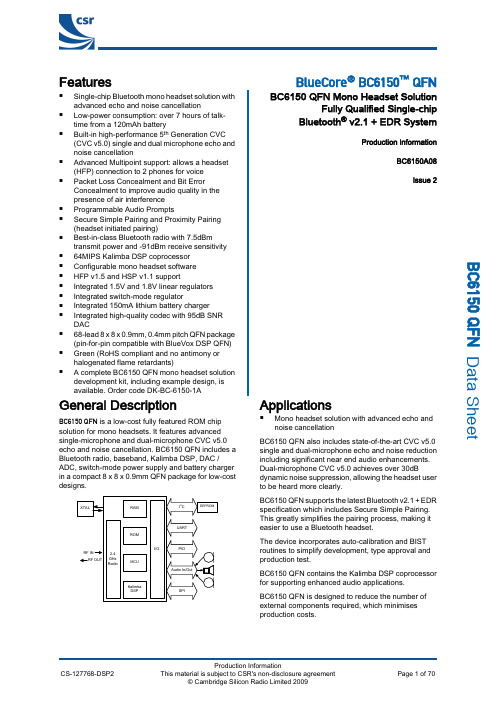
Features _äìÉ`çêÉ∆=_`SNRM »=nck■Single-chip Bluetooth mono headset solution withadvanced echo and noise cancellation ■Low-power consumption: over 7 hours of talk-time from a 120mAh battery ■Built-in high-performance 5th Generation CVC(CVC v5.0) single and dual microphone echo and noise cancellation■Advanced Multipoint support: allows a headset (HFP) connection to 2 phones for voice■Packet Loss Concealment and Bit Error Concealment to improve audio quality in thepresence of air interference■Programmable Audio Prompts■Secure Simple Pairing and Proximity Pairing(headset initiated pairing)■Best-in-class Bluetooth radio with 7.5dBmtransmit power and -91dBm receive sensitivity■64MIPS Kalimba DSP coprocessor■Configurable mono headset software■HFP v1.5 and HSP v1.1 support■Integrated 1.5V and 1.8V linear regulators■Integrated switch-mode regulator■Integrated 150mA lithium battery charger■Integrated high-quality codec with 95dB SNRDAC■68-lead 8 x 8 x 0.9mm, 0.4mm pitch QFN package(pin-for-pin compatible with BlueVox DSP QFN)■Green (RoHS compliant and no antimony orhalogenated flame retardants)■ A complete BC6150 QFN mono headset solutiondevelopment kit, including example design, isavailable. Order code DK‑BC‑6150‑1ABC6150 QFN Mono Headset SolutionFully Qualified Single-chipBluetooth ® v2.1 + EDR SystemProduction InformationBC6150A08Issue 2General Description _`SNRM=nck is a low-cost fully featured ROM chip solution for mono headsets. It features advanced single-microphone and dual-microphone CVC v5.0echo and noise cancellation. BC6150 QFN includes a Bluetooth radio, baseband, Kalimba DSP, DAC /ADC, switch-mode power supply and battery charger in a compact 8 x 8 x 0.9mm QFN package for low-cost designs.Applications■Mono headset solution with advanced echo andnoise cancellationBC6150 QFN also includes state-of-the-art CVC v5.0single and dual-microphone echo and noise reductionincluding significant near end audio enhancements.Dual-microphone CVC v5.0 achieves over 30dBdynamic noise suppression, allowing the headset userto be heard more clearly.BC6150 QFN supports the latest Bluetooth v2.1 + EDRspecification which includes Secure Simple Pairing.This greatly simplifies the pairing process, making iteasier to use a Bluetooth headset.The device incorporates auto-calibration and BISTroutines to simplify development, type approval andproduction test.BC6150 QFN contains the Kalimba DSP coprocessorfor supporting enhanced audio applications.BC6150 QFN is designed to reduce the number ofexternal components required, which minimisesproduction costs._`SNRM=nck Data SheetDocument History RevisionDate Change Reason127 AUG 09Original publication of this document.213 NOV 09Production Information added.SPI interface information updated.If you have any comments about this document, email comments@ givingthe number, title and section with your feedback.Document History_`SNRM=nck Data SheetStatus InformationThe status of this Data Sheet is Production Information .CSR Product Data Sheets progress according to the following format:Advance InformationInformation for designers concerning CSR product in development. All values specified are the target values of thedesign. Minimum and maximum values specified are only given as guidance to the final specification limits and mustnot be considered as the final values.All detailed specifications including pinouts and electrical specifications may be changed by CSR without notice.Pre-production InformationPinout and mechanical dimension specifications finalised. All values specified are the target values of the design.Minimum and maximum values specified are only given as guidance to the final specification limits and must not beconsidered as the final values.All electrical specifications may be changed by CSR without notice.Production InformationFinal Data Sheet including the guaranteed minimum and maximum limits for the electrical specifications.Production Data Sheets supersede all previous document versions.Life Support Policy and Use in Safety-critical ApplicationsCSR's products are not authorised for use in life-support or safety-critical applications. Use in such applications isdone at the sole discretion of the customer. CSR will not warrant the use of its devices in such applications.CSR Green Semiconductor Products and RoHS ComplianceBC6150 QFN devices meet the requirements of Directive 2002/95/EC of the European Parliament and of the Councilon the Restriction of Hazardous Substance (RoHS).BC6150 QFN devices are also free from halogenated or antimony trioxide-based flame retardants and otherhazardous chemicals. For more information, see CSR's Environmental Compliance Statement for CSR GreenSemiconductor Products .Trademarks, Patents and LicencesUnless otherwise stated, words and logos marked with ™ or ® are trademarks registered or owned by CSR plc or itsaffiliates. Bluetooth ® and the Bluetooth ® logos are trademarks owned by Bluetooth ® SIG, Inc. and licensed toCSR. Other products, services and names used in this document may have been trademarked by their respectiveowners.The publication of this information does not imply that any license is granted under any patent or other rights ownedby CSR plc and/or its affiliates.CSR reserves the right to make technical changes to its products as part of its development programme.While every care has been taken to ensure the accuracy of the contents of this document, CSR cannot acceptresponsibility for any errors.Refer to for compliance and conformance to standards information.Status Information_`SNRM=nck Data SheetContents1Device Details (8)2Functional Block Diagram (9)3Package Information (10)3.1Pinout Diagram (10)3.2Device Terminal Functions (11)3.3Package Dimensions (15)3.4PCB Design and Assembly Considerations (16)3.5Typical Solder Reflow Profile (16)4Bluetooth Modem (17)4.1RF Ports (17)4.1.1RF_N and RF_P (17)4.2RF Receiver (17)4.2.1Low Noise Amplifier (17)4.2.2RSSI Analogue to Digital Converter (17)4.3RF Transmitter (18)4.3.1IQ Modulator (18)4.3.2Power Amplifier (18)4.4Bluetooth Radio Synthesiser (18)4.5Baseband (18)4.5.1Burst Mode Controller (18)4.5.2Physical Layer Hardware Engine (18)4.6Basic Rate Modem (18)4.7Enhanced Data Rate Modem (18)5Clock Generation (20)5.1Clock Architecture (20)5.2Input Frequencies and PS Key Settings (20)5.3External Reference Clock (20)5.3.1Input: XTAL_IN (20)5.3.2XTAL_IN Impedance in External Mode (21)5.3.3Clock Start-up Delay (21)5.3.4Clock Timing Accuracy (21)5.4Crystal Oscillator: XTAL_IN and XTAL_OUT (22)5.4.1Load Capacitance (23)5.4.2Frequency Trim (23)5.4.3Transconductance Driver Model (24)5.4.4Negative Resistance Model (24)5.4.5Crystal PS Key Settings (25)6Bluetooth Stack Microcontroller (26)6.1Programmable I/O Ports, PIO and AIO (26)7Kalimba DSP (27)8Memory Interface and Management (28)8.1Memory Management Unit (28)8.2System RAM (28)8.3Kalimba DSP RAM (28)8.4Internal ROM (28)9Serial Interfaces (29)9.1UART Interface (29)9.1.1UART Configuration While Reset is Active (31)9.2Programming and Debug Interface (31)9.2.1Instruction Cycle ..................................................................................................................... 31_`SNRM=nck Data Sheet9.2.2Multi-slave Operation (31)9.3I 2C Interface (31)10Audio Interface (33)10.1Audio Input and Output (33)10.2Mono Audio Codec Interface (33)10.2.1Mono Audio Codec Block Diagram (34)10.2.2ADC (34)10.2.3ADC Digital Gain (34)10.2.4ADC Analogue Gain (35)10.2.5DAC (35)10.2.6DAC Digital Gain (35)10.2.7DAC Analogue Gain (36)10.2.8Microphone Input (36)10.2.9Output Stage (39)10.2.10Side Tone (40)10.2.11Integrated Digital Filter (40)11Power Control and Regulation (42)11.1Power Sequencing (42)11.2External Voltage Source (42)11.3Switch-mode Regulator (43)11.4Low-voltage Linear Regulator (43)11.5Low-voltage Audio Linear Regulator (43)11.6Voltage Regulator Enable Pins (44)11.7Battery Charger (44)11.8LED Drivers (44)11.9Reset, RST# (45)11.9.1Digital Pin States on Reset (46)11.9.2Status after Reset (46)12Example Application Schematic (47)13Electrical Characteristics (48)13.1ESD Precautions (48)13.2Absolute Maximum Ratings (48)13.3Recommended Operating Conditions (48)13.4Input/Output Terminal Characteristics (49)13.4.1Low-voltage Linear Regulator (49)13.4.2Low-voltage Linear Audio Regulator (50)13.4.3Switch-mode Regulator (51)13.4.4Battery Charger (52)13.4.5Reset (53)13.4.6Regulator Enable (53)13.4.7Digital Terminals (54)13.4.8Mono Codec: Analogue to Digital Converter (55)13.4.9Mono Codec: Digital to Analogue Converter (56)13.4.10Clocks (57)13.4.11LED Driver Pads (57)13.4.12Auxiliary ADC (58)14Power Consumption (59)15CSR Green Semiconductor Products and RoHS Compliance (61)15.1RoHS Statement (61)15.1.1List of Restricted Materials (61)16BC6150 QFN Software Stack (62)16.1BC6150 QFN Mono Headset Solution Development Kit (62)16.2BC6150 QFN Mono Headset Solution ................................................................................................. 62_`SNRM=nck Data Sheet16.3Advanced Multipoint Support (62)16.4Programmable Audio Prompts (63)16.5Proximity Pairing (63)16.5.1Proximity Pairing Configuration (63)17Ordering Information (64)17.1BC6150 QFN Mono Headset Solution Development Kit Ordering Information (64)18Tape and Reel Information (65)18.1Tape Orientation (65)18.2Tape Dimensions (65)18.3Reel Information (66)18.4Moisture Sensitivity Level (66)19Document References (67)Terms and Definitions (68)List of FiguresFigure 2.1Functional Block Diagram (9)Figure 3.1Device Pinout (10)Figure 3.2Package Dimensions (15)Figure 4.1Simplified Circuit RF_N and RF_P (17)Figure 4.2BDR and EDR Packet Structure (19)Figure 5.1Clock Architecture (20)Figure 5.2TCXO Clock Accuracy (22)Figure 5.3Crystal Driver Circuit (22)Figure 5.4Crystal Equivalent Circuit (23)Figure 7.1Kalimba DSP Interface to Internal Functions (27)Figure 9.1Universal Asynchronous Receiver (29)Figure 9.2Break Signal (30)Figure 9.3Example EEPROM Connection (32)Figure 10.1BC6150 QFN Audio Interface (33)Figure 10.2Mono Codec Audio Input and Output Stages (34)Figure 10.3ADC Analogue Amplifier Block Diagram (35)Figure 10.4Microphone Biasing (36)Figure 10.5Speaker Output (40)Figure 11.1Voltage Regulator Configuration (42)Figure 11.2LED Equivalent Circuit (45)Figure 12.1Example Application Schematic (47)Figure 16.1Programmable Audio Prompts in External I 2C EEPROM (63)Figure 18.1BC6150 QFN Tape Orientation (65)Figure 18.2Reel Dimensions (66)List of TablesTable 4.1Data Rate Schemes (19)Table 5.1External Clock Specifications (21)Table 5.2Crystal Specification (23)Table 9.1Possible UART Settings (29)Table 9.2Standard Baud Rates (30)Table 9.3Instruction Cycle for a SPI Transaction (31)Table 10.1ADC Digital Gain Rate Selection (34)Table 10.2DAC Digital Gain Rate Selection (35)Table 10.3DAC Analogue Gain Rate Selection (36)Table 10.4Voltage Output Steps ....................................................................................................................... 38_`SNRM=nck Data SheetTable 10.5Current Output Steps (39)Table 11.1BC6150 QFN Voltage Regulator Enable Pins (44)Table 11.2BC6150 QFN Digital Pin States on Reset (46)List of EquationsEquation 5.1Load Capacitance (23)Equation 5.2Trim Capacitance (23)Equation 5.3Frequency Trim (24)Equation 5.4Pullability (24)Equation 5.5Transconductance Required for Oscillation (24)Equation 5.6Equivalent Negative Resistance (25)Equation 9.1Baud Rate (30)Equation 10.1IIR Filter Transfer Function, H(z) (41)Equation 10.2IIR Filter plus DC Blocking Transfer Function, H DC(z) (41)Equation 11.1LED Current (45)Equation 11.2LED PAD Voltage (45)_`SNRM=nckData Sheet1Device DetailsRadio ■Common TX/RX terminal simplifies external matching; eliminates external antenna switch ■BIST minimises production test time ■Bluetooth v2.1 + EDR specification compliant Transmitter ■7.5dBm RF transmit power with level control from a 6-bit DAC over a typical 30dB dynamic range ■Class 2 and Class 3 support without the need for an external power amplifier or TX/RX switch Receiver ■Receiver sensitivity of -91dBm ■Integrated channel filters ■Digital demodulator for improved sensitivity and co-channel rejection ■Real-time digitised RSSI available on HCI interface ■Fast AGC for enhanced dynamic range Synthesiser ■Fully integrated synthesiser requires no external VCO, varactor diode, resonator or loop filter ■Compatible with crystals 16MHz to 26MHz or an external clock 12MHz to 52MHz Kalimba DSP ■Very low power Kalimba DSP coprocessor,64MIPS, 24-bit fixed point core ■Single-cycle MAC; 24 x 24-bit multiply and 56-bit accumulator ■32-bit instruction word, dual 24-bit data memory■6K x 32-bit program RAM, 8K x 24-bit + 8K x 24-bit data RAM ■64 x 32-bit program memory cache when executing from ROM Audio Codec ■16-bit internal codec ■ADC and DAC for stereo audio ■Integrated amplifiers for driving 16Ω speakers; no need for external components ■Support for single-ended speaker termination and line output ■Integrated low-noise microphone bias Physical Interfaces ■Synchronous serial interface for system debugging ■I²C compatible interface to external EEPROMcontaining device configuration data (PS Keys)■UART interface with data rates up to 3Mbits/s■Bidirectional serial programmable audio interfacesupporting PCM, I²S and SPDIF formats■ 2 LED drivers with fadersBaseband and Software■Internal ROM■48KB of internal RAM, allows full-speed datatransfer, mixed voice/data and full piconet support■Logic for forward error correction, header errorcontrol, access code correlation, CRC,demodulation, encryption bit stream generation,whitening and transmit pulse shaping■Transcoders for A-law, µ-law and linear voice fromhost and A-law, µ-law and CVSD voice over air■Configurable mono headset ROM software to set-up headset features and user interface■Support for HFP v1.5 (including three-way calling)and HSP v1.1■Support for Bluetooth v2.1 + EDR specificationSecure Simple Pairing■Proximity Pairing (headset initiated pairing)■Advanced Multipoint support, allowing the headsetto connect to 2 mobile phones or 1 mobile phoneand a VoIP dongle■Programmable audio prompts■Packet Loss Concealment and Bit ErrorConcealment to improve audio quality in thepresence of air interference■DSP based single-microphone CVC v5.0 echo andnoise cancellation is included in the BC6150 QFNfor effective noise cancellation under all conditions■ A high-performance dual-microphone noisecancellation is available using CVC v5.0 is availablein BC6150 QFN providing over 30dB of dynamicnoise suppressionAuxiliary Features■Crystal oscillator with built-in digital trimming■Power management includes digital shutdown andwake-up commands with an integrated low-poweroscillator for ultra-low power Park/Sniff/Hold mode■Clock request output to control external clock■On-chip regulators: 1.5V output from 1.7V to 1.95Vinput■On-chip high-efficiency switched-mode regulator:1.8V output from2.5V to 4.4V input■Power-on-reset cell detects low-supply voltage■10-bit ADC available to applications■On-chip 150mA charger for lithium ion/polymerbatteriesPackage Option■QFN 68-lead, 8 x 8 x 0.9mm, 0.4mm pitch Device Details_`SNRM=nck Data Sheet2Functional Block DiagramG-TW-0115.3.2VREGIN_AUDIO VDD_AUDIO VREGENABLE_L VREGIN_L VREGENABLE_H VSS BAT_PVDD_CHG RF_P XTAL_OUT XTAL_IN LO_REF VDD_LO LED[0]VDD_PADSVDD_MEM RST#TEST_ENVDD_SMP_CORE VDD_CORE VDD_ANA LX VDD_RADIO LED[1]AIO[0]AIO[1]PIO[5:0]VSS_PIO VDD_PIO PIO[14:11, 9]RF_N SPKR_A_PSPKR_A_NMIC_BIASMIC_A_PMIC_A_NMIC_B_NMIC_B_PAU_REF_DCPLUART_TXUART_RXUART_CTS UART_RTS VDD_UARTPIO[7]PIO[8]PIO[6]SPI_CS#SPI_MISO SPI_MOSISPI_CLKFigure 2.1: Functional Block DiagramFunctional Block Diagram_`SNRM=nck Data Sheet3Package Information 3.1Pinout DiagramG-TW-091.4.21234567891018192011121314151617212223242526272829303132333435363738394041424344454647484950515268535455565758596061626364656667Orientation from Top of DeviceFigure 3.1: Device Pinout Package Information_`SNRM=nck Data Sheet3.2Device Terminal FunctionsBluetooth Radio Lead Pad Type Supply Domain DescriptionRF_N65RFVDD_RADIO Transmitter output/switched receiverRF_P64RF Complement of RF_N Synthesiser andOscillatorLead Pad Type Supply Domain DescriptionXTAL_IN3Analogue VDD_ANA For crystal or external clock inputXTAL_OUT4Drive for crystalLO_REF5Reference voltage to decouple the synthesiserSPI Interface Lead Pad Type Supply Domain DescriptionSPI_MOSI28Input, with weak internal pull-downVDD_PADSSPI data inputSPI_CS#30Bidirectional with weakinternal pull-downChip select for SPI, active lowSPI_CLK29Bidirectional with weakinternal pull-downSPI clockSPI_MISO31Bidirectional with weakinternal pull-downSPI data outputUART Interface Lead Pad Type Supply Domain DescriptionUART_TX9Output, tri-state, with weakinternal pull-downVDD_UARTUART data output, active highUART_RX10Bidirectional with weakinternal pull-downUART data input, active highUART_RTS12Bidirectional CMOS output,tri-state, with weak internalpull-upUART request to send active lowUART_CTS11CMOS input with weakinternal pull-downUART clear to send active low_`SNRM=nckData SheetPIO Port Lead Pad Type Supply Domain Description PIO[14]20Bidirectional withprogrammable strength internal pull-up/down VDD_PADS Programmable input/output linePIO[13]19PIO[12]18PIO[11]15PIO[9]14PIO[8]21PIO[7]22PIO[6]23PIO[5]24PIO[4]25PIO[3]58Bidirectional withprogrammable strength internal pull-up/down VDD_PIO Programmable input/output linePIO[2]59PIO[1]60PIO[0]61AIO[1]6Bidirectional VDD_ANA Programmable input/output line AIO[0]7_`SNRM=nck Data SheetAudio Lead Pad Type Supply Domain DescriptionSPKR_A_N56Analogue VDD_AUDIO Speaker output, negative, channel ASPKR_A_P57Analogue VDD_AUDIO Speaker output, positive, channel AMIC_A_N52Analogue VDD_AUDIO Microphone input, negative, channel AMIC_A_P51Analogue VDD_AUDIO Microphone input, positive, channel AMIC_B_N50Analogue VDD_AUDIO Microphone input, negative, channel BMIC_B_P48Analogue VDD_AUDIO Microphone input, positive, channel BMIC_BIAS45Analogue VDD_AUDIO,BAT_PMicrophone biasAU_REF_DCPL55Analogue VDD_AUDIO Decoupling of audio reference, for high-quality audioLED Drivers Lead Pad Type Supply Domain Description LED[1]33Open drain output Open drainLED driver LED[0]32LED driver Test and Debug Lead Pad Type Supply Domain DescriptionRST#26Input with weak internal pull-upVDD_PADSReset if low. Input debounced somust be low for >5ms to cause aresetTEST_EN27Input with strong internal pull-downFor test purposes only, leaveunconnected_`SNRM=nckData SheetPower SuppliesControl Lead DescriptionVREGENABLE_L68Low-voltage linear regulator and low-voltage audiolinear regulator enable, active highVREGIN_L 1Input to internal low-voltage regulatorVREGENABLE_H 35Switch-mode regulator enable, active highVREGIN_AUDIO 46Input to internal audio low-voltage linear regulator VDD_AUDIO 47Positive supply for audioLX 37Switch-mode regulator outputVDD_ANA 2Positive supply output for analogue circuitry and1.5V regulated output, from internal low-voltageregulatorVDD_PIO 62Positive supply for digital input/output ports PIO[3:0]VDD_PADS 16Positive supply for all other digital Input/Output portsincluding PIO[14:11,9:4]VDD_CORE 17, 34Positive supply for internal digital circuitryVDD_RADIO 63, 66Positive supply for RF circuitryVDD_UART 13Positive supply for UART portsVDD_LO 67Positive supply for local oscillator circuitryBAT_P 38Lithium ion/polymer battery positive terminal. Batterycharger output and input to switch-mode regulatorVDD_CHG 39Lithium ion/polymer battery charger inputVDD_SMP_CORE 36Positive supply for switch-mode control circuitry VSS Exposed Pad Ground connectionsUnconnected Leads (N/Cs)Description8, 40, 41, 42, 43, 44, 49, 53, 54Leave unconnected_`SNRM=nck Data Sheet3.3Package DimensionsG-T W-0939.4.3Orientation from TopSeating PlaneOrientation from BottomFigure 3.2: Package Dimensions_`SNRM=nck Data Sheet3.4PCB Design and Assembly ConsiderationsThis section lists recommendations to achieve maximum board-level reliability of the 8 x 8 x 0.9mm QFN 68-leadpackage:■NSMD lands (lands smaller than the solder mask aperture) are preferred, because of the greater accuracy of the metal definition process compared to the solder mask process. With solder mask defined pads, theoverlap of the solder mask on the land creates a step in the solder at the land interface, which can causestress concentration and act as a point for crack initiation.■CSR recommends that the PCB land pattern to be in accordance with IPC standard IPC-7351.■Solder paste must be used during the assembly process.3.5Typical Solder Reflow ProfileSee Typical Solder Reflow Profile for Lead-free Devices for information._`SNRM=nckData Sheet4Bluetooth Modem4.1RF Ports4.1.1RF_N and RF_PRF_N and RF_P form a complementary balanced pair and are available for both transmit and receive. On transmit their outputs are combined using an external balun into the single-ended output required for the antenna. Similarly,on receive their input signals are combined internally.Both terminals present similar complex impedances that may require matching networks between them and the balun. Viewed from the chip, the outputs can each be modelled as an ideal current source in parallel with a lossy capacitor. An equivalent series inductance can represent the package parasitics.G-T W-03349.2.2RF_NRF_PFigure 4.1: Simplified Circuit RF_N and RF_PRF_N and RF_P require an external DC bias. The DC level must be set at VDD_RADIO.4.2RF ReceiverThe receiver features a near-zero IF architecture that allows the channel filters to be integrated onto the die. Sufficient out-of-band blocking specification at the LNA input allows the receiver to be used in close proximity to GSM and W‑CDMA cellular phone transmitters without being desensitised. The use of a digital FSK discriminator means that no discriminator tank is needed and its excellent performance in the presence of noise allows BC6150 QFN to exceed the Bluetooth requirements for co-channel and adjacent channel rejection.For EDR, the demodulator contains an ADC which digitises the IF received signal. This information is then passed to the EDR modem.4.2.1Low Noise AmplifierThe LNA operates in differential mode and takes its input from the shared RF port.4.2.2RSSI Analogue to Digital ConverterThe ADC implements fast AGC. The ADC samples the RSSI voltage on a slot-by-slot basis. The front-end LNA gain is changed according to the measured RSSI value, keeping the first mixer input signal within a limited range. This improves the dynamic range of the receiver, improving performance in interference limited environments._`SNRM=nck Data Sheet4.3RF Transmitter4.3.1IQ ModulatorThe transmitter features a direct IQ modulator to minimise frequency drift during a transmit timeslot, which results in a controlled modulation index. Digital baseband transmit circuitry provides the required spectral shaping.4.3.2Power AmplifierThe internal PA has a maximum output power that allows BC6150 QFN to be used in Class 2 and Class 3 radios without an external RF PA.4.4Bluetooth Radio SynthesiserThe Bluetooth radio synthesiser is fully integrated onto the die with no requirement for an external VCO screening can, varactor tuning diodes, LC resonators or loop filter. The synthesiser is guaranteed to lock in sufficient time across the guaranteed temperature range to meet the Bluetooth v2.1 + EDR specification.4.5Baseband4.5.1Burst Mode ControllerDuring transmission the BMC constructs a packet from header information previously loaded into memory-mapped registers by the software and payload data/voice taken from the appropriate ring buffer in the RAM. During reception, the BMC stores the packet header in memory-mapped registers and the payload data in the appropriate ring buffer in RAM. This architecture minimises the intervention required by the processor during transmission and reception.4.5.2Physical Layer Hardware EngineDedicated logic performs the following:■Forward error correction■Header error control■Cyclic redundancy check■Encryption■Data whitening■Access code correlation■Audio transcodingFirmware performs the following voice data translations and operations:■A-law/µ-law/linear voice data (from host)■A-law/µ-law/CVSD (over the air)■Voice interpolation for lost packets■Rate mismatch correctionThe hardware supports all optional and mandatory features of Bluetooth v2.1 + EDR specification including AFH and eSCO.4.6Basic Rate ModemThe basic rate modem satisfies the basic data rate requirements of the Bluetooth v2.1 + EDR specification. The basic rate was the standard data rate available on the Bluetooth v1.2 specification and below, it is based on GFSK modulation scheme.Including the basic rate modem allows BC6150 QFN compatibility with earlier Bluetooth products.The basic rate modem uses the RF ports, receiver, transmitter and synthesiser, alongside the baseband components described in Section 4.5.4.7Enhanced Data Rate ModemThe EDR modem satisfies the requirements of the Bluetooth v2.1 + EDR specification. EDR has been introduced to provide 2x and 3x data rates with minimal disruption to higher layers of the Bluetooth stack. BC6150 QFN supportsboth the basic and enhanced data rates and is compliant with the Bluetooth v2.1 + EDR specification._`SNRM=nck Data SheetAt the baseband level, EDR uses the same 1.6kHz slot rate and the 1MHz symbol rate defined for the basic data rate. EDR differs in that each symbol in the payload portion of a packet represents 2 or 3 bits. This is achieved using 2 new distinct modulation schemes. Table 4.1 and Figure 4.2 summarise these. Link Establishment and Management are unchanged and still use GFSK for both the header and payload portions of these packets.The enhanced data rate modem uses the RF ports, receiver, transmitter and synthesiser, with the baseband components described in Section 4.5.Data Rate Scheme Bits Per Symbol ModulationBasic Rate 1GFSKEDR 2π/4 DQPSKEDR 38DPSK (optional)Table 4.1: Data Rate SchemesG-TW-0244.2.3Enhanced Data Rate Figure 4.2: BDR and EDR Packet Structure_`SNRM=nck Data Sheet。

Phase-locked loopStructure and functionPhase-locked loop mechanisms may be implemented as either analog or digital circuits. Both implementations use the same basic structure. Both analog and digital PLL circuits include four basic elements:▪Phase detector,▪Low-pass filter,▪Variable-frequency oscillator, and▪feedback path (which may include a frequency divider).VariationsThere are several variations of PLLs. Some terms that are used are analog phase-locked loop (APLL) also referred to as a linear phase-locked loop (LPLL), digital phase-locked loop (DPLL), all digital phase-locked loop (ADPLL), and software phase-locked loop (SPLL).Analog or Linear PLL (LPLL)Phase detector is an analog multiplier. Loop filter is active or passive. Uses a V oltage-controlled oscillator(VCO).Digital PLL (DPLL)An analog PLL with a digital phase detector (such as XOR, edge-trigger JK, phase frequency detector). May have digital divider in the loop.All digital PLL (ADPLL)Phase detector, filter and oscillator are digital. Uses a numerically controlled oscillator (NCO).Software PLL (SPLL)Functional blocks are implemented by software rather than specialized hardware. Performance parameters▪Type and order▪Lock range: The frequency range the PLL is able to stay locked. Mainly defined by the VCO range.▪Capture range: The frequency range the PLL is able to lock-in, starting from unlocked condition. This range is usually smaller than the lock range and willdepend e.g. on phase detector.▪Loop bandwidth: Defining the speed of the control loop.▪Transient response: Like overshoot and settling time to a certain accuracy (like 50ppm).▪Steady-state errors: Like remaining phase or timing error▪Output spectrum purity: Like sidebands generated from a certain VCO tuning voltage ripple.▪Phase-noise: Defined by noise energy in a certain frequency band (like 10kHz offset from carrier). Highly dependent on VCO phase-noise, PLL bandwidth, etc.▪General parameters: Such as power consumption, supply voltage range, output amplitude, etc.ApplicationsPhase-locked loops are widely used for synchronization purposes; in space communications for coherent demodulation and threshold.extension, bit synchronization, and symbol synchronization. Phase-locked loops can also be used to demodulate frequency-modulated signals. In radio transmitters, a PLL is used to synthesize new frequencies which are a multiple of a reference frequency, with the same stability as the reference frequency.Other applications include:▪Demodulation of both FM and AM signals▪Recovery of small signals that otherwise would be lost in noise (lock-in amplifier)▪Recovery of clock timing information from a data stream such as from a disk drive▪Clock multipliers in microprocessors that allow internal processor elements to run faster than external connections, while maintaining precise timing relationships▪DTMF decoders, modems, and other tone decoders, for remote control and telecommunicationsClock recoverySome data streams, especially high-speed serial data streams (such as the raw stream of data from the magnetic head of a disk drive), are sent without an accompanying clock. The receiver generates a clock from an approximate frequency reference, and then phase-aligns to the transitions in the data stream with a PLL. This process is referred to as clock recovery. In order for this scheme to work, the data stream must have a transition frequently enough to correct any drift in the PLL's oscillator. Typically, some sort of redundant encoding is used, such as8b/10b encoding. DeskewingIf a clock is sent in parallel with data, that clock can be used to sample the data. Because the clock must be received and amplified before it can drive the flip-flopswhich sample the data, there will be a finite, and process-, temperature-, and voltage-dependent delay between the detected clock edge and the received data window. This delay limits the frequency at which data can be sent. One way of eliminating this delay is to include a deskew PLL on the receive side, so that the clock at each data flip-flop is phase-matched to the received clock. In that type of application, a special form of a PLL called a delay-locked loop (DLL) is frequently used.Clock generationMany electronic systems include processors of various sorts that operate at hundreds of megahertz. Typically, the clocks supplied to these processors come from clock generator PLLs, which multiply a lower-frequency reference clock (usually 50 or 100 MHz) up to the operating frequency of the processor. The multiplication factor can be quite large in cases where the operating frequency is multiple gigahertz and the reference crystal is just tens or hundreds of megahertz.Spread spectrumAll electronic systems emit some unwanted radio frequency energy. Various regulatory agencies (such as the FCC in the United States) put limits on the emitted energy and any interference caused by it. The emitted noise generally appears at sharp spectral peaks (usually at the operating frequency of the device, and a few harmonics).A system designer can use a spread-spectrum PLL to reduce interference with high-Q receivers by spreading the energy over a larger portion of the spectrum. For example, by changing the operating frequency up and down by a small amount (about 1%), a device running at hundreds of megahertz can spread its interference evenly over a few megahertz of spectrum, which drastically reduces the amount of noise seen on broadcast FM radio channels, which have a bandwidth of several tens of kilohertz. Clock distributionTypically, the reference clock enters the chip and drives a phase locked loop (PLL), which then drives the system's clock distribution. The clock distribution is usually balanced so that the clock arrives at every endpoint simultaneously. One of those endpoints is the PLL's feedback input. The function of the PLL is to compare the distributed clock to the incoming reference clock, and vary the phase and frequency ofits output until the reference and feedback clocks are phase and frequency matched. PLLs are ubiquitous—they tune clocks in systems several feet across, as well as clocks in small portions of individual chips. Sometimes the reference clock may not actually be a pure clock at all, but rather a data stream with enough transitions that the PLL is able to recover a regular clock from that stream. Sometimes the reference clock is the same frequency as the clock driven through the clock distribution, other times the distributed clock may be some rational multiple of the reference.Jitter and noise reductionOne desirable property of all PLLs is that the reference and feedback clock edges be brought into very close alignment. The average difference in time between the phases of the two signals when the PLL has achieved lock is called the static phase offset (also called the steady-state phase error). The variance between these phases is called tracking jitter. Ideally, the static phase offset should be zero, and the tracking jitter should be as low as possible.Phase noise is another type of jitter observed in PLLs, and is caused by the oscillator itself and by elements used in the oscillator's frequency control circuit. Some technologies are known to perform better than others in this regard. The best digital PLLs are constructed with emitter-coupled logic (ECL) elements, at the expense of high power consumption. To keep phase noise low in PLL circuits, it is best to avoid saturating logic families such as transistor-transistor logic (TTL) or CMOS.[citation needed]Another desirable property of all PLLs is that the phase and frequency of the generated clock be unaffected by rapid changes in the voltages of the power and ground supply lines, as well as the voltage of the substrate on which the PLL circuits are fabricated. This is called substrate and supply noise rejection. The higher the noise rejection, the better.To further improve the phase noise of the output, an injection locked oscillator can be employed following the VCO in the PLL.Frequency SynthesisIn digital wireless communication systems (GSM, CDMA etc.), PLLs are used to provide the local oscillator for up-conversion during transmission and down-conversion during reception. In most cellular handsets this function has been largely integrated into a single integrated circuit to reduce the cost and size of the handset. However, due to the high performance required of base station terminals, the transmission and reception circuits are built with discrete components to achieve the levels of performance required. GSM local oscillator modules are typically built with a frequency synthesizer integrated circuit and discrete resonator VCOs.Frequency synthesizer manufacturers include Analog Devices, National Semiconductor and Texas Instruments. VCO manufacturers include Sirenza, Z-Communications, Inc.Phase-locked loop block diagramDigital phase-locked loop block diagramA phase detector compares two input signals and produces an error signal which is proportional to their phase difference. The error signal is then low-pass filtered and used to drive a VCO which creates an output phase. The output is fed through an optional divider back to the input of the system, producing a negative feedback loop. If the output phase drifts, the error signal will increase, driving the VCO phase in the opposite direction so as to reduce the error. Thus the output phase is locked to the phase at the other input. This input is called the reference.Analog phase locked loops are generally built with an analog phase detector, low pass filter and VCO placed in a negative feedback configuration. A digital phase locked loop uses a digital phase detector; it may also have a divider in the feedback path or in the reference path, or both, in order to make the PLL's output signal frequency a rational multiple of the reference frequency. A non-integer multiple of the reference frequency can also be created by replacing the simple divide-by-N counter in the feedback path with a programmable pulse swallowing counter. This technique is usually referred to as a fractional-N synthesizer or fractional-N PLL.The oscillator generates a periodic output signal. Assume that initially the oscillator is at nearly the same frequency as the reference signal. If the phase from the oscillator falls behind that of the reference, the phase detector changes the control voltage of the oscillator so that it speeds up. Likewise, if the phase creeps ahead of the reference, the phase detector changes the control voltage to slow down the oscillator. Since initially the oscillator may be far from the reference frequency, practical phase detectors may also respond to frequency differences, so as to increase the lock-in range of allowable inputs.Depending on the application, either the output of the controlled oscillator, or the control signal to the oscillator, provides the useful output of the PLL system.Phase detectorThe two inputs of the phase detector are the reference input and the feedback from the VCO. The PD output controls the VCO such that the phase difference between the two inputs is held constant, making it a negative feedback system. There are severaltypes of phase detectors in the two main categories of analog and digital.Different types of phase detectors have different performance characteristics.For instance, the frequency mixer produces harmonics that adds complexity in applications where spectral purity of the VCO signal is important. The resulting unwanted sidebands, also called "reference spurs" can dominate the filter requirements and reduce the capture range and lock time well below the requirements. In these applications the more complex digital phase detectors are used which do not have as severe a reference spur component on their output. Also, when in lock, the steady-state phase difference at the inputs using this type of phase detector is near 90 degrees. The actual difference is determined by the DC loop gain.A bang-bang charge pump phase detector must always have a dead band where the phases of inputs are close enough that the detector detects no phase error. For this reason, bang-bang phase detectors are associated with significant minimum peak-to-peak jitter, because of drift within the dead band.However these types, having outputs consisting of very narrow pulses at lock, are very useful for applications requiring very low VCO spurious outputs. The narrow pulses contain very little energy and are easy to filter out of the VCO control voltage. This results in low VCO control line ripple and therefore low FM sidebands on the VCO.In PLL applications it is frequently required to know when the loop is out of lock. The more complex digital phase-frequency detectors usually have an output that allows a reliable indication of an out of lock condition.ModelingTime domain modelThe equations governing a phase-locked loop with an analog multiplier as the phase detector and linear filter may be derived as follows. Let the input to the phase detector be xr(θr(t))and the output of the VCO is xc(θc(t))with phases θr(t)and θc(t).Functions xc(θ) and xr(θ) describe waveforms of signals. Then the output of the phasedetector xm(t) is given byxm(t) = xr(θr(t))xc(θc(t))the VCO frequency is usually taken as a function of the VCO input g(t) aswhere gv is the sensitivity of the VCO and is expressed in Hz / V; ωc is a free-running frequency of VCO.The Loop Filter can be described by system of linear differential equationswhere xm(t) is an input of the filter, xf(t) is an output of the filter, A is n-by-n matrix,. represents an initial state of the filter. The star symbol is a conjugate transpose.Hence the following system describes PLLwhere φ0 is an initial phase shift.Phase domain modelConsider the input of pll xr(θr(t))and VCO output xc(θc(t))are high frequency signals. Then for any piecewise differentiable 2π-periodic functions xr(θ) and xc(θ) there is a function φ(θ) such that the output G(t) of Filterin phase domain is asymptotically equal ( the difference G(t) −xf(t)is small with respect to the frequencies) to the output of the Filter in time domain model.Here function φ(θ) is a phase detector characteristic.Denote by θe(t) the phase differenceθe = θr(t) −θc(t).Then the following dynamical system describes PLL behaviorHere ωe = ωr−ωc; ωr is a frequency of reference oscillator( we assume that ωr is constant).ExampleConsider sinusoidal signalsand simple one-pole RC circuit as a filter. Time domain model takes formPD characteristics for this signals is equal[14] toHence the phase domain model takes formThis system of equations is equivalent to the equation of mathematical pendulumLinearized phase domain modelPhase locked loops can also be analyzed as control systems by applying the Laplace transform. The loop response can be written as:Where▪θo is the output phase in radians▪θi is the input phase in radians▪Kp is the phase detector gain in volts per radian▪Kv is the VCO gain in radians per volt-second▪F(s) is the loop filter transfer function (dimensionless)The loop characteristics can be controlled by inserting different types of loop filters. The simplest filter is a one-pole RC circuit. The loop transfer function in this case is:The loop response becomes:This is the form of a classic harmonic oscillator. The denominator can be related to that of a second order system:Where▪ζ is the damping factor▪ωn is the natural frequency of the loopFor the one-pole RC filter,The loop natural frequency is a measure of the response time of the loop, and the damping factor is a measure of the overshoot and ringing. Ideally, the natural frequency should be high and the damping factor should be near 0.707 (critical damping). With a single pole filter, it is not possible to control the loop frequency and damping factor independently. For the case of critical damping,A slightly more effective filter, the lag-lead filter includes one pole and one zero. This can be realized with two resistors and one capacitor. The transfer function for this filter isThis filter has two time constantsτ1 = C(R1 + R2)τ2 = CR2Substituting above yields the following natural frequency and damping factorThe loop filter components can be calculated independently for a given natural frequency and damping factorReal world loop filter design can be much more complex e.g. using higher order filters to reduce various types or source of phase noise.锁相环结构和功能锁相环机制,可以实现模拟或数字电路。
conformance test capabilities.The AC1036 conformance test option verifies and thoroughly documents that your handset s signaling software conforms to current TIA/EIA-136 series specifications. Full AMPS testing modes are available with theThe FM/AM-1600S/CSA gives you full featuredIdeal for conformance and protocol testing of UWC-136 base stations and terminalsFM/AM-1600S/CSAcapabilities, full level control and measurement facilities of modulation, and precision power meter features for enhanced sensitivity and high accuracy testing needs.Analog paging encoding/decoding,DTMF , tone coded squelch, digital squelch,AM modulation/demodulation with two separate AF generators and a cross band duplex feature gives you added test versatility in a variety of public and private wireless systems.Software Options Make Complex Testing SimpleAs with every IFR test set, you get the advantage of IFR applications engineering support.Our comprehensive portfolio of application software options is designed to automate and expand the functionality of your instrument.Plus, on-going software support means that you can easily upgrade your FM/AM-1600S/CSA when standards definitions or test and service requirements change.AC1009W - EasySpan is a Windows-based software utility which extracts spectrum analyzer and trackinggenerator traces from the IFR FM/AM-1600S/CSA to a PC for furtheroff-line analysis.AC1011 - Simultaneously analyzes thesignal strength or channel activity of upto three voice channel groups or 100frequencies. AC1012 - AutoCell 882 is acomprehensive test package for Ericsson model 882 base station transceivers.AC1017 - AutoCell-Series II is a comprehensive program for FCCcompliance testing of Lucent Series II cell sites.AC1018 - Provides automated testing and calibration of Motorola HD-II/LD cellsites. AC1019 - EasySweep is a sweptmeasurement utility designed to test antennas and transmission lines. AC1020D - AutoCell NT and AutoCell NTD provides automated testing of Northern Telecom cell sites.Dynamic IQ Constellation Display Simplifies AnalysisThe FM/AM-1600S/CSA provides you with a dynamic, high speed constellation display for precise RF modulation analysis of π/4 DQPSK digitally modulatedwaveforms from 10 MHz to 1 GHz. This unique FM/AM-1600S/CSA feature gives a near-real time display of digital modulation characteristics that points out the cause of the trouble in digital radios.IQ Constellation display allows for comprehensivedigital modulation testingComplex Functionality Made EasyEven with its elaborate capabilities, theFM/AM-1600S/CSA was developed to execute complex tests simply and withminimal operator ing field-proven front panel and user man-machine interfaces, the FM/AM-1600S/CSA gives you the performance and ease-of-use features thatsignificantly reduce your testing andtraining time.Its test macro command programming language (TMAC) can be easily configuredto perform complex automatic tests on base stations and terminals (includingsingle and multi-mode as well as singleand multi-band radios), and baseband equipment. This powerful capability allowsyou to create and save simple "one button"test routines for future use. This flexibilitymeans you can create and execute complex and repeatable routines no matter what your level of expertise.A color display gives FM/AM-1600S/CSA users vivid screen clarity. Extensive use of softkeys reduces your complex cellular and PCS parametric and protocol tests to fast,simple and manageable routines.Specification (T/R & DUPLEX CONNECTORS)Frequency Range 400 kHz to 999.9999 MHzResolution 100 HzAccuracy Same as Master OscillatorOutput Level Range (T/R)-137 dBm to 0 dBm into 50 Ω(-40 dBm maximum with reverse power present)Duplex Level Range-120 dBm to + 7 dBm or into 50 ΩDuplex Resolution 0.1 dBLevel Accuracy (T/R)±1.5 dB (level ≥-110 dBm)±2.5 dB (levels from <-110 dBm to -127 dBm)Duplex Level Accuracy±1.5 dB (level ≥-100 dBm)±2.5 dB (levels from <-100 dBm to -120 dBm)VSWR (T/R)<1.35:1 typical Duplex VSWR <1.38:1INPUT PROTECTION (T/R)See RF Power Meter(DUPLEX)65 W (15 seconds with alarm)SPECTRAL PURITY Harmonics <-26 dBc Non-Harmonics <-50 dBcResidual FM<10 Hz (RMS, 0.3 kHz to 3 kHz BW)Residual AM<0.05% (RMS, 0.3 kHz to 3 kHz BW)SSB Phase Noise<-90 dBc/Hz (25 kHz offset)<-85 dBc/Hz (25 kHz offset, f c ≥930 MHz)<-80 dBc/Hz (25 kHz offset, f c <1 MHz)Internal FM RangeOff, 100 Hz to 100 kHz Dev Accuracy±5% (1 kHz to 25 kHz Dev, 1 kHz rate)±7% (<1 kHz Dev and >25 kHz Dev, 1 kHz rate)Resolution100 Hz (≤25 kHz Dev)500 Hz (>25 kHz Dev)Rate Off, 30 Hz to 40 kHz (≤20 kbs digital)Waveforms Sine, Square, Triangle, Ramp and PulseDistortion <1 % (1 kHz rate, 0.3 kHz to 3 kHz BW,1 kHz to 25 kHz deviation)INTERNAL AM RF GENERATORRange 500 kHz to 999.9999 MHz Internal AM Range Off, 1% to 90%Accuracy±5% of setting (30% to 90% modulation, 1 kHz sinewave)±10% of setting (30% to 90% modulation, 1 kHz sinewave f c< 1 MHz)Resolution 1 %Rate 100 Hz to 10 kHz WaveformsSine, Square, Triangle, Ramp and Pulse Distortion <1% (30% to 70% modulation, 1 kHz sinewave, f c>1 MHz, 0.3 kHz to 3 kHz BW)Internal Phase Modulation Range Off, 0.1 to 10 Radians Accuracy ±10% (at 1 kHz rate, > 0.3 Rad)Resolution 0.1 Radians Rate Off, 30 Hz to 6 kHz Waveforms Sine, Square, Triangle, Ramp and Pulse Distortion<2% (1 kHz rate, 0.3 kHz to 3 kHz BW, ≥0.5 Rad)ExternalExternal inputs with the same characteristics as the internal modulation sources are supported.A 10 Vp-p injection level is required to obtain indicated setting ±10%.Modulation RF Signal Generator FM/AM-1600S/CSAFM/AM-1600S/CSASynthesizer Switching Speed Settling Time1.5 ms (within 1 kHz of desired frequency, 1 MHz ≤f c <100 MHz, 25 kHz steps)2.5 ms (within 1 kHz of desired frequency, 400 kHz ≤f c ≤999.9999 MHz, 100 Hz steps)AF GENERATORS #1 AND #2Frequency Range 10 Hz to 40 kHzFrequency Resolution0.1 Hz (≤2 kHz), 1 Hz (>2 kHz)Frequency Accuracy ±0.1%Level Range0.5 mV RMS to 2.5 VRMS (into 150 Ω)Up to 3 VRMS (into 600 Ω)Level Resolution0.1 mV RMS (10 mVRMS to 200 mVRMS)0.8 mV RMS (> 200 mVRMS)Level Accuracy±0.1 mV or < 3% (≤10 kHz, into 150 Ω) ±5% (10 kHz to 25 kHz, into 150 Ω)SPECTRAL PURITYTHD<0.25% (sinewave, 10 Hz to 1.1 kHz,>100 mV RMS)<1% (sinewave, 1.1 kHz to 35 kHz,>100 mV RMS)WaveshapeSinewave, Square, Triangle, Ramp and PulseRange10 Hz to 40 kHz (in 4 decade ranges)AccuracySame as Master Oscillator Resolution0.1 Hz (10 Hz to ≤2 kHz)1 Hz (>2 kHz to ≤20 kHz)10 Hz (>20 kHz to 40 kHz)Input Waveform Sine or SquareExternal Level0.5 VRMS to 30 VRMS (SINAD/BER input)0.1 VRMS to 3.5 VRMS (EXT MOD input)Impedance1 M Ω(SINAD/BER input) 100 k Ω(EXT MOD input)Signal Selections Demod Audio SINAD/BER AF Generators RF PowerExternal Audio RF COUNTERFrequency Range250,000 Hz to 999,999,990 Hz AccuracySame as Master Oscillator Resolution1 Hz (f c <20 MHz) 10 Hz (f c ≥20 MHz)Level-10 dBm to +50 dBm (T/R connector) -80 dBm to +10 dBm (ANT connector)Digital Meter Range 0 Hz to ± 150 kHzBar Graph Meter Range0 to ±100 kHz (in 4 decade ranges)AccuracySame as Master Oscillator Resolution1 Hz (±1 Hz to ≤±10 kHz)10 Hz (> ±10 kHz to ±150 kHz)Level-10 dBm to +50 dBm (T/R connector)-80 dBm to +10 dBm (ANT connector)Frequency Range 1.5 MHz to 1 GHzInput Level0.2 mW to 200 WRanges20 mW to 200 W full scale (1-2-5 sequence)Resolution 0.1 mWAccuracy±10% ±2 countsVSWR<1.15:1 (0.25 MHz ≤f c ≤100 MHz)<1.23:1 (100 MHz <f c ≤400 MHz)<1.38:1 (400 MHz <f c ≤999.9999 MHz)Frequency Range400 kHz to 999.9999 MHzSensitivity≤2 µV for 10 dB SINAD(1 kHz rate, 6 kHz Dev, FM 1)RX IFAF Selectivity ModeBandwidth Bandwidth FM 4300 kHz 100 kHz FM 3300 kHz 20 kHz FM 230 kHz 10 kHz FM 130 kHz 3 kHz AM 1 2.9 kHz 3 kHz AM 230 kHz 10 kHz USB 2.9 kHz 3 kHz LSB 2.9 kHz 3 kHz PM30 kHz3 kHzAdjacent Channel RejectionRX IF Bandwidth >30 dB Down300 kHz ±485 kHz maximum 30 kHz ±52 kHz maximum 2.9 kHz±2.5 kHz maximumDEMODULATION OUTPUTOutput Level (FM)5 Vp-p ±10% (at full scale, into 600 Ω)(PM)40 mV RMS ±10% (5 Rad, into 600 Ω)(AM)1 VRMS ±10%(80% modulation, into 600 Ω)(SSB)1. 15 VRMS ±10% (Beat tone, into 600 Ω)DISTORTION + NOISE(FM)<2% (1 kHz rate, >1 kHz Dev,0.3 kHz to 3 kHz BW)(AM)<2% (1 kHz rate, 30% to 90% modulation, 0.3 kHz to 3 kHz BW)Impedance <1 ΩANT Input Protection≤65 W for 15 sec with alarm Range±100 kHz (± peak in 6 ranges)Resolution50 Hz (≤20 kHz ranges)1 kHz(>20 kHz ranges)Accuracy±4% ±2 counts + source residual (300 kHz IF , <15 kHz rate)±7% ±2 counts + source residual (300 kHz IF , ≥15 kHz rate)±7% ± 2 counts + source residual (30 kHz IF)Rate100 Hz to 40 kHzCarrier Range400 kHz to 999.9999 MHzCarrier Level-10 dBm to +50 dBm (T/R connector)-70 dBm to +10 dBm (ANT connector)Range0 Rad to 10 Rad (Peak)Resolution0.01 Rad (≤5 Rad)0.1 Rad (>5 Rad)Accuracy±3% full scale ±1 count + source residual Rate300 Hz to 4 kHzCarrier Range400 kHz to 999.9999 MHzCarrier Level-10 dBm to +50 dBm (T/R connector)-80 dBm to +10 dBm (ANT connector)Range:1% to 100%Resolution 1 %Accuracy±5% of full scale ±1 count + source residual (30% to 90%)Rate100 Hz to 10 kHzCarrier Range400 kHz to 999.9999 MHzCarrier Level-10 dBm to +50 dBm (T/R connector)-80 dBm to +10 dBm (ANT connector)Distortion Range 0.1 % to 20 %Resolution 0.1 %Accuracy±0.5 % distortion ±1 count (1 % to 10 %)±2 % distortion ±1 count (>1 % to 20 %)Signal Frequency 600 Hz to 1.4 kHz Range3 dB to 30 dB Resolution 0.1 dBAccuracy±1 dB ±1 count (@12 dB SINAD)Signal Level0.1 VRMS to 30 VRMS (SINAD/BER input)Input RangeNT 400 ChannelsCellular 800 MHz Channels Minimum Carrier Level -60 dBm (ANT connector)EVM Range 0 to 100 %EVM Resolution 0.01 %Meter Residual EVM <2 % indicationAccuracy±3.0% indication, ±1 LSD + meter residual EVMFM/AM-1600S/CSAFM/AM-1600S/CSAIFR Americas, Inc., 10200 West York Street, Wichita, Kansas67215-8999,USA.E-mail:***************Tel: +1 316 522 4981 Toll Free USA: 1 800 835 2352 Fax: +1 316 522 1360As we are always seeking to improve our products, the information in this document gives only a general indication of the product capacity, performance and suitability, none of which shall form part of any contract. We reserve the right to make design changes without notice. All trademarks are acknowledged. Parent Company IFR Systems, Inc. © IFR Ltd. 1999.FM/AM-1600S/CSA。
colon n.冒号dash n.连接号comma n.逗号underscore n.下划线discipline n.学科fundamental s n.基本原理corollary n.推论assume v.假设assessment n.评估assignment n.任务access n.通道入口v.接近accurate adj.准确的精确的analysis n.分析elementary adj.基础的algebra n.代数calculus n.微积分probability n.概率论prescribe v.规定指示开药方protocol n. (数据传输)协议laboratory n. 实验课conduct v.组织实施指挥enforce v.实施强迫fundamental adj.基本的comprehensive adj.综合的comprehension n.理解力complement n.补充second half 下半场revise v.复习修正reinforce v.增强review v.复习notify v.通知公告notification n. 通知subsequent adj.随后的curriculum n.课程circuit n.电路v. 环行router n.路由器server n.服务器projector n.投影仪analogous adj.类似的analogue adj.模拟的n.类似物analogy n.类比propagate v.传播普及繁衍accelerate v.加速framework n.结构框架dispensable adj.非必需的indispensable adj.必不可少的terminology n.术语deploy v.部署有效利用module n.单元模块modulate v.调制调节modulation n.调制model n/v. 模型做模型建模modem 等于modulator-demodulator n.调制解调器cellular adj.蜂窝的细胞的interference n.干涉干扰slide n.幻灯片v.滑动降低slice v./n.薄片切precise adj.精确的heterogeneous adj.多种多样由不同组成的homogeneous adj.同类的由相同组成的(uniform)无线通信:spectrum n.谱频谱声谱spectral adj.domain n.范围领域定义域域time domain时域frequency domain频域transmit v.传输传播发射transmitter n.发射机receiver n.接收机binary adj.二进制的bipolar adj.两极的双极性的repeater n.中继器转发器electromagnetic noise电磁干扰electromagnetic wave 电磁波interfere v.干扰阻碍interference n.interval n.间隔conjugate adj.共轭的distort v.扭曲失真distortion n.失真variance n.方差变化不一致variation n.变化mean n.平均值standard deviation 标准差covariance n.协方差integration n.积分integrate v.使结合一体化求积分derivation n.导数derivate v.派生衍生求导derive v.导出源于获得corrupted adj.损坏的腐败的modulation n.调制demodulation n.解调amplitude n.振幅广阔丰富detection n.检测检波imaginary part 虚部real part 实部imaginary adj.虚构的想象的虚部的proximity n.接近临近proximate adj.近似的最接近的obstruct v.阻塞阻碍obstructed adj. unobstructed adj.decay v.腐朽衰败衰落attenuation n.衰减attenuate v.antenna gain 天线增益unitless 无单位的partition n./v.分裂隔板隔开random variable 随机变量conductor n.导体指挥检票员fluctuate v.波动carrier n.载波inter-symbol interference 符号间干扰ISIreplica n.复制副本overlap n./v.重叠convolution n.卷积convolute v.回旋卷绕discrete system 离散系统decompose v.分解腐烂sequence n.序列impulse n.脉冲一般指冲激信号velocity n.速率threshold n.阈值临界值coherent adj.相干的连贯的synchronize v.同步同时发生synchronization n.phase n.相位phasor n.矢量相量(包括幅度和角度)amplify v.放大增强dashed line虚线millisecond n.毫秒hexagon n.六角形prone adj.有...的倾向的易于...的deteriorate v.恶化退化sectorial adj.扇形的sectorization n.分段化扇形化sector n.扇形align v.校准对其一致alignment n.电信网络:topology n.拓扑学memory n.内存buffer n./v.缓存缓冲allocate v.分配指定拨出slot n./v.空挡位置idle adj./v.空闲的闲置的懒惰的congestion n.拥挤充血占线音congest v. busy tone 忙音processor n.处理器nodal adj.节点的encapsulation n.封装encapsulate v.压缩封入内部decapsulate v.解封装intermittent adj.间歇性的retrieve v.检索,恢复,取回identifer n.标识符proprietary adj.专有的专利的specification n.说明规范cleartext password 明文密码encrypt v.加密encryption n.intact adj.完好无损的integrate v.整合adj.完全的hierarchical adj.分层次的分等级的iterate v.迭代iteration n.recursive adj.递归的congest v.充血拥塞congestion n.idle adj./v.空闲的懒惰的encapsulate v.封装constrain v.约束constraint n.约束条件consent n./v.同意准许collision n.冲突collide v.reassemble v.重新装配fragment v./n.碎片片段payload n.有效负荷净负荷enumerate v.枚举列举数学相关:diagram n.图表v.用图表法histogram n.直方图柱状图exponential adj.指数的exponent n.指数orthogonal adj.正交的proportional adj.成比例的statistical adj.统计的integer n.整数constant n.常数variable n.变量symmetrical adj.对称的biased adj.偏的有偏见的bias n.偏见偏差arithmetic n./adj.算数算数的computation n.计算formula n.公式megabyte n.1MB mega百万10^6multi前缀多…multiple adj.多重的复杂的n.倍数multiply v.乘繁殖domain定义域range 值域slope n.斜率parameter n.参数加and/plus/added to 减minus/taken from/subtracted from subtraction减法4 plus 6 equals to 10. 8 minus 3 is 5.4 added to 6 is 10. 3 taken(subtracted) from 8 leaves 5.乘time/multiplied by 除divided to/into3 times 5 is 15. 8 into 24 equals 3.3 multiplies by 5 is 15. 24 divided by 8 is 3.3/4 three fourth s24/25 twenty-four twenty-fifth s10^7 the 7th power of 10 10 to the 7th powerx分之y y over xtranspose v.移项变换顺序转置multiplication n.相乘power n.幂4 to the power of 3. 4的3次方exponential adj./n.指数的logarithm n.对数logarithmic adj.initialization n.初始化probability n.概率proportional adj.成比例的linear adj.线性的nolinear adj.非线性的equation n.方程式fraction n.分数比例率coefficient n.系数denote v.表示指代(记为)threshold n.临界值阈值门槛converge v.趋于收敛于diameter n.直径weighted adj.加权的directed adj.有向的time-varying adj.时变的bifurcate v./adj. 分叉分支chaotic adj.无序的混沌的mutual adj.相互的共有的internal adj.内部的国内的external adj.外部的国外的fractal n.不规则形分形adjacent adj.相邻的shift v.移动替换transition n.转变过渡discrete adj.离散的分离的column n.列圆柱row n.行cylinder n.圆柱体identical adj.同一的identity n.同一性身份identify v.识别等同于geometric n.几何的denominator n.分母numerator n.分子2D continuous function 二维连续函数origin n.原点开端起源coordinate system 坐标系diagonal n./adj.对角线斜线density n.密度dense adj.稠密的密度大的normalized adj.标准化归一化dimensionless n.无穷小量dimension n.方面维3Dinverse adj./n.相反的倒转的倒数reciprocal n./adj.倒数的相互的交互的product n.乘积normal distribution 正态分布square n./adj.平方正方形monotonic adj.单调的argument n.自变量binomial n./adj. 二项式binomial distribution 二项分布inequality n.不等式不平等intersection n.交集交叉点intersect v.相交交叉横穿union n.并集编程相关:syntax n.语法句法tuple n. 数组set n.集合array n.数组package n.软件包extract n./v.提取摘录matrix n.矩阵loop n.循环iterate v.迭代execute v.执行function n.函数parameter n.参数segment n.段部分v.分割划分algorithm n.算法conjecture n.猜想theory n.理论theorem n.定理colon n.冒号interface n.界面v.连接交流图像处理:format n.格式v.格式化formation n.形成组成extract v.提取convert v.转变转换merge v.合并split v.分离划分slice v.切割RGB和BGR蓝绿红ROI: region of interestpixel n.像素photosite n.像素attribute n.属性variable n.变量element n.元素要素degrade v.退化降低degradation n.compress v.压缩compression n.压缩deburr v.清理毛刺blur n./v.模糊motion n./v.运动移动Spatial quantization 空间的量化intensity n.强度intense adj.强烈的紧张的激烈的inpainting n.图像修复texture n.质地实质纹理segment v.分割划分segmentation n.分割partition v.分割partitioning n.extract v.提取storage n.储存transmit v.传输发送transfer v.转移translate v.翻译shift v.转移换convert v.转变换算transition n.过渡转变transit v.运送经过lossy adj.有损耗的lossy compression 有损压缩acquire v.获得acquisition n.获得采集capture v.采集捕捉引起sensor n.传感器individual n.个人adj.单独的charge v./n.收费充电电荷accumulate v.累积horizontal adj./n.水平的水平面horizon n.地平线vertical adj./n.垂直的垂直线vertex n.顶点voltage n.电压volume n.体积amplify v.放大增强register v./n.注册登记显示shift register n.移位寄存器interpolate v.篡改插入mosaic n./v.马赛克demosaic v.去马赛克illuminate v.照亮阐明illumination n.光源灯饰启示illustrate v.举例说明digital adj.数字的digitize v.数字化analog n./adj.模拟analog image 模拟图像index n.索引(复数indexes/indices)denote v. 表示指示标志imply v.表示暗示donate v.捐赠sample n./v. 采样取样quantization n.量化quantize v.scan v./n.扫描discrete adj.分离的离散的continuous adj.连续的coordinate v.协作搭配n.坐标coordinate system 坐标系resolution n.解决决心分辨率interpolation n.插入插值填写interpolate v.resize v.调整大小real-time 实时的ultrasound n.超声波capacitor n.电容器circuit n.电路回路环线circuitry n.电路电路图prism n.棱镜棱柱contour n./v.轮廓边界线abrupt adj.突然的不连贯的tuple n.元组hue n.色调saturation n.饱和度offset n.偏移量gain n.增益clip v.剪掉裁剪template n.样板模板intermediate adj./n.中间的中间事物intermediate image 中间过渡图像eliminate v.消除淘汰flip v.反转打开overlap v.重叠superimpose v.叠加magnitude n.大小数值periodic adj.周期的series n.级数系列mitigate v.减轻缓和ramp n.斜坡坡道渐变notate v.以符号标记notation n.记法符号conjugate v./adj./n.共轭complex conjugate 复共轭harmonics n.谐波impulse train冲击序列translation v.平移翻译replica n.复制副本dilated adj.扩大膨胀dilate v. dilation n.sinusoid 正弦曲线aliasing n.混叠wrap v./n.包裹环绕围巾卷饼wraparound error 环绕错误suppress v.抑制阻止mitigate v.使减轻使缓和transition n.过渡转变transit v.运输经过agenda n.议程表待议日程arithmetic n.算数运算arithmetical adj. algorithm n.算法geometry n.几何geometric adj. medium adj.中间的五分熟的平均的median adj./n.中间值中位数prior adj.先前的正式的prior probability先验概率matrix n.矩阵metric n.度量标准adj.十进制的trim v.修剪调整emit v.发出发射beam n.光线波束project v.投射预测projection n.投影diffuse v./adj.扩散弥漫漫反射传播synchronous adj.同步的synchrony n.intercept n./v.截距拦截截断slope n./v.斜率倾斜斜坡vector n.矢量向量unit vector单位向量prime n.上标撇slash n.斜杠arbitrary adj.任意的recap n.扼要重述preliminary adj./n.初步的预赛transpose n./v.转置调换erode v.腐蚀削弱erosion n.腐蚀dilate v.膨胀扩大dilation n.膨胀shrink v.缩水缩小减少fracture v.断裂破碎duality n.二元性对偶性optimize v.优化optimal adj.最佳的合适的speckled adj.有斑点的speckle n./v.斑点色斑做标记多维数据:regress v./n..倒退回归regression n.回归set v.放n.集合anomaly n.异常asymmetric adj.不对称的sparse adj.稀疏的sparsity n.稀疏性symmetry n.对称相似induce v.引起诱使inductive adj.归纳的诱导的induction n.归纳感应deduct v.演绎扣除deduction n.推论split v./n.分割划分sort v./n.分类排序permute v.改变顺序permutation n.categorize v.分类category n. categorical adj.分类的绝对的numeric adj.数值的quantitative adj.定量的数量的qualitative adj.定性的质量的autocorrelation 自相关temporal autocorrelation 时间自相关temporal adj.时间的暂时的redundant adj.多余的冗余converge v.收敛聚集convergence n.复杂网络:homogeneous adj.单一的均匀的同质的isomorphic adj.同构的同形的isomorphism n.bipartite adj.双向的二分的invertible adj.可逆的traverse v.穿过横越yield v./n.产生出产产量skeleton n.骨骼框架梗概backbone n.脊柱骨干initial adj.最初的首字母outlier n.离群值异常值局外人consensus n.共识一致看法counterclockwise 逆时针clockwise顺时针equilibrate v.使平衡equilibrium n.均衡平衡rational adj.理智的hierarchies n.层级分层分类sparse adj.稀疏的稀少的benchmark n.比较基准synchrony n.同步synchronization n.同时性同步性consensus n.共识检测估计:hypothesis n.假设猜想scenario n.场景terminology n.术语interpolate v.插入篡改defect n.缺点v.背叛crude adj.粗略的粗糙的abrupt adj.突然的陡峭的唐突的asymptotic adj.渐进的渐近线的marginal adj.边缘的微不足道的marginal probability边缘概率prior probability先验概率conditional probability条件概率posterior probability后验概率hypothesis testing假设检验ground truth真实值decision region决策域disjoint adj.不相交的overlap adj.重叠的curvature n.弧线曲率concave adj.凹的power spectral density能量谱密度inner product 内积点积norm 模transpose v.调换n.转置矩阵determinant n./adj.决定因素行列式subscript n./adj.下标注脚Wide Sense Stationary 广义平稳time invariant时不变discretize v.离散discrete adj.离散的distort v.失真扭曲superimpose v.叠加compose v.组成构成移动APP:tablet n.药片平板电脑agenda n.待议事项议事日程kernel n.核内核compiler n.编译器compile v.汇编编译搜集manifest adj./n.表明显示清单configurate v.配置使形成obfuscate v.使模糊混淆refine v.改进精炼virtual adj.虚拟的实际上的device driver 设备驱动程序accelerate v.加速促进template n.模板样板compact adj./n.紧凑的简洁的deploy v.部署调动配置refactor v./n.重构configure v.配置config=configuration n.配置install v.安装icon n.图标palette n.调色板选项板compatible adj.兼容的可共处的execute v.执行实施prototype v./n.原型雏形widget n.小工具窗口小部件toggle n./v.切换转换(键)embed v.嵌入内置portrait adj.纵向的n.肖像描绘纵向打印格式vertical adj.垂直的纵向的landscape adj.横向打印格式n.风景横向打印格式v.景观美化horizontal adj.水平的chaos n.混乱无序状态chaotic adj.混乱的enclose v.封装围住封上nest v./n.鸟巢嵌套一套物件align v.对齐使一致margin v./n.边缘利润余地custom n.顾客惯例adj.定做的自定义的current adj.当前的流行的n.水流concurrency n.并发性并行性thread n.线程v.穿起来asynchronous adj.异步的instantiate v.举例说明invoke v.调用提及引起sequential adj.按顺序的相继发生的dispatch n./v.派遣发送迅速处理parse v.分析解析immutable adj.不可改变的mutable adj.可变的易变的explicit adj.明确的详述的implicit adj.含蓄的facilitate v.促进使便利synchronize v.同步grant v./n.承认给予授予engage v.从事雇佣pane n.玻璃窗格repository n.数据库储藏室资源库retrieve n.找回检索refactor v./n.重构resume v.恢复重新开始customize v.定制排队论:stochastic adj.随机的stochastic process 随机过程swap v.交换替换constraint n.约束条件constrain v.约束限制强迫moderate adj.适中的温和的中等的regime n.制度状态机制ethical adj.道德的plagiarize v.抄袭剽窃plagiarism n.mutually exclusive events 互斥事件mutual adj.相互的exclusive adj.昂贵的独有的排斥的rigorous adj.严格的严密的novel n.小说novelty adj./n.新颖的新奇的事物intersection n.交集相交交点在B的条件下A的概率the probability of A given Bposterior probability后验概率posterior adj.其次的较后的prior probability先验概率prior adj.先前的优先的axiom n.公理定理binomial n./adj.二项分布geometric n./adj.几何分布uniform distribution均匀分布recursion n.递归循环recur v.再发生反复出现arbitrary adj.任意的estimator n.估计量估计函数revise v./n.修正复习denominator n.分母numerator n.分子numerous adj.许多的fraction n.分数decimal n.小数integer n.整数expected value 期望standard deviation 标准差covariance n.协方差preliminary n./adj.初步的预备的准备工作identity n.身份特征同一性identical adj.同一的完全相同的stationary adj.不动的平稳的strictly stationary严格平稳ergodicity n. 遍历性各态历经性ergodic adj.multivariate adj.多元的多变量的superpose v.叠加叠放superposition n.叠加lag v./n.掉队延迟滞后consecutive adj.连续的derive v.起源于获得导出derivation n.求导导数validate v.正式确认生效物联网:mindset n.思维模式trend n.趋势风尚curriculum n.课程combat v.战斗争论block diagram 狂徒converge v.集中汇集convergence n.汇集融合immersive adj.沉浸式immerse v.沉浸于浸没resistor n.电阻resistance n.电阻(值)accelerate v.加速促进acceleration n.加速度accelerometer n.加速度计acoustic adj./n.声音的声学appliance n.家用电器actuator n.执行器驱动器actuate v.驱动促使velocity n.速度displacement n.位移gravity n.重力coordinate v./n.协调坐标magnetometer n.磁力计magnetic adj.磁性的axis n.轴对称轴calibrate v.校准calibration n.校准刻度vibrate v.震动vibration n.震动oscillate v.振荡oscillation n.振荡gearbox n.变速箱utilize v.利用使用日常:obsess v.痴迷blackout v.断电propagate v.传播繁殖grid n.格子lattice n.格子pervade v.遍及弥漫prominent adj.突出的杰出的tremendous adj.极大的极棒的intrinsic adj.内在的disordered adj.杂乱的错乱的convention n.约定协定condense v.压缩浓缩eliminate v.消除淘汰consensus n.一致同意initial adj.最初的字首的initialization n.初始化interrelated adj.相互关联的interpersonal adj.人与人之间的split v.分离skip v.跳过conform v.遵守符合顺应cluster n.群formation n.形成formative adj.形成的有重大影响的format v.格式化n.格式subtle adj.细微的敏感的verify v.核实查证vary v.变化variation n.变化variant adj.变化的vertical adj.垂直的duplicate n./v./adj.完全一样的复制implement v.实施penalty n.惩罚penalize v.惩罚capital n./adj.大写lowercase n./adj.小写specify v.具体指出specific adj.明确的特定的respective adj.各自的分别的estimate v.估计assign v.赋值分配assignment n.任务作业execute v.执行valid adj.有效的合法的vivid adj.生动的鲜艳的dynamic adj.动态的有活力的compose v. 组成撰写排版decompose v.分解腐烂spectrum n.范围频谱光谱perceptual adj.感知的有知觉的perception n.认知知觉洞察力absorb v.吸收掌握scope n.范围视野dissipate v.驱散挥霍mandatory adj.强制的tedious adj.单调乏味的allude v.略微提到暗指discern v辨别了解recognize v.识别承认decompose v.分解腐烂衰变deficient adj. deficiency n.不足缺陷interval n.间隔desirable adj.令人满意的满足需要的complement n./v.补充pros and cons(拉丁语) 优缺点nuts and bolts(螺母和螺栓) 基本组成部分aka (also known as)又叫做ultimate adj.最终的最重要的configuration n.布局配置configure v.安装形成hybrid n./adj.混合杂种immune adj.免疫的不受影响的layman n.外行门外汉exceed v.超越超过incoming adj.进来的进入的income n.收入alter v.改变修改alternate v./adj.交替轮流alternative adj./n.可选择的二选一alternatively adv.要不二择一on-demand adj.按需的emphasize v.强调negligible adj.可以忽略的precede v. 在之前的领先experiment v./n.实验尝试arbitrary adj.任意的suffice v.足够有能力sufficient adj.elastic adj.弹性的灵活的essentially adv.本质上实质上essential adj.必须的基本的excess adj./n.超额的过多的violate v.违反侵犯compose v.撰写组成排版compromise n./v.折中妥协intuitive adj.直觉的intuition n.直觉lengthy adj.冗长的过于详尽的grasp v./n.握紧领会characterize v.描述刻画convention n.习俗公约conventional adj.依照惯例的criterion n.标准规范criteria 复数interpret v.解释口译interpretation n.解释notation n.符号标记法mutual adj.相互的sketch v./n.绘制草图outage n.断电中断in all walks of life 在各行各业frontier n./adj.边境前沿embark v.开始着手上船possess v.具备拥有insight n.了解洞察力encounter v.遭遇碰到inherent adj.固有的内在的与生俱来的inherently adv. commonality n.共性sophisticated adj.复杂精妙的水平高的stepping stone 跳板垫脚石bracket n.括号圆括号square bracket 方括号superscript n.上角标hypothesis n.猜想假设submarine v./n./adj.海底的潜水艇。
文章编号:1671-637Ⅹ(2008)022*******光纤光栅传感系统信号解调新技术研究王 瑜, 乔学光, 傅海威, 禹大宽, 马 超, 张 晶(西安石油大学陕西省光电传感测井重点实验室,西安 710065)摘 要: 信号解调是光纤光栅传感系统实用化所面临的最大难题,其核心问题在于设计高分辨率、低成本的波长检测方案。
总结了光纤光栅传感信号解调的一般原理和技术难点,对常用解调方法进行了分类和归纳。
目前报道的主要解调方法是滤波法、干涉法和可调光源扫描法。
针对不同的解调方法,重点介绍了它们的工作原理及性能特点,评价了其优缺点,并分别给出了它们的实验原理图。
对目前最有应用前景的可调谐F-P滤波法进行了详细的介绍和分析,并加入了对原有方案的改进,用气体吸收池代替原来的参考光栅。
关 键 词: 光纤传感; 光纤光栅传感; 信号解调; 波长编码中图分类号: V243.1文献标识码: AN e w demodulation technologies for fiberBragg grating sensing systemW ANG Y u, QI AO Xue2guang, FU Hai2wei, Y U Da2kuan, M A Chao, ZH ANGJing(Shanxi K ey Laboratory o f Photoeletric Sensing Logging,Xi’an Petroleum Univer sity,Xi’an710065,China)Abstract: Signal dem odulation is one of the m ost com plicated problems in practical application of fiber grat2 ing sens or system,and the core issue lies in the design of a wave2length examination scheme that has higher res olution and lower cost.The general principle and the technical difficulties of the fiber grating sens or system signal dem odulation are summarized,and the comm only2used dem odulation methods are classified.The main dem odulation techniques reported currently are:filter dem odulation,interference scanning dem odulation and tunable s ource dem odulation methods.The principle of operation,characteristics and functions of the methods are discussed,their advantages and disadvantages are analyzed,typical schemes of experiments are given re2 spectively.The tunable F2P filter dem odulation method,which has the widest application prospect,is intro2 duced in detail.We made s ome im provement to the original scheme by using gas cell to replace the original reference F BG.K ey w ords: fiber sens or; Fiber Bragg G rating(F BG)sens or; signal dem odulation; wavelength encode0 引言近年来,在光纤通信迅猛发展的带动下,光纤传感器作为传感器家族中年轻的一员,以其在抗电磁收稿日期:2006210212 修回日期:2006211206基金项目:中国石油天然气集团公司应用基础研究项目(20050719);陕西省教育厅产业化培育项目(05JC23);西安市科技局信息技术专项项目(Z X05041)作者简介:王 瑜(1983-),女,陕西咸阳人,硕士,主要从事光纤传感及信号解调方面的研究。
光纤通信中常用英文缩写Acron ymsa c alt ernat ing c urren t 交变电流交流A M amp litud e mod ulati on 幅度调制AO N all-opti cal n etwor k 全光网络APD aval anche phot odiod e 雪崩二极管AS E amp lifie d spo ntane ous e missi on 放大自发辐射ASK a mplit ude s hiftkeyin g 幅移键控ATM asyn chron ous t ransf er mo de 异步转移模式BER b it er ror r ate 误码率BH buri ed he teros truct ure 掩埋异质结BPF b and p ass f ilter带通滤波器C3cleav ed-co upled cavi ty 解理耦合腔C ATV c ommon ante nna c abletelev ision有线电视CDMcodedivis ion m ultip lexin g 码分复用CNR carr ier t o noi se ra tio 载噪比CS O Com posit e sec ond o rder复合二阶CPFSK cont inuou s-pha se fr equen cy-sh ift k eying连续相位频移键控CVD c hemic al va pourdepos ition化学汽相沉积CW cont inuou s wav e 连续波DBRdistr ibute d Bra gg re flect or 分布布拉格反射DFBdistr ibute d fee dback分布反馈dc d irect curr ent 直流DCF disp ersio n com pensa tingfiber色散补偿光纤DS F dis persi on sh ift f iber色散位移光纤DIP dual in l ine p ackag e 双列直插DPS K dif feren tialphase-shif t key ing 差分相移键控EDFA erbi um do ped f iberampli fier掺铒光纤激光器FD DI fi ber d istri buted data inte rface光纤数据分配接口FDM f reque ncy d ivisi on mu ltipl exing频分复用FETfield effe ct tr ansis tor 场效应管F M fre quenc y mod ulati on 频率调制FP Fabr y Per ot 法布里里-珀落FSKfrequ ency-shift keyi ng 频移键控FW HM fu ll wi dth a t hal f max imum半高全宽FWM f our-w ave m ixing四波混频GVDgroup-velo citydispe rsion群速度色散HBT hete rojun ction-bipo lar t ransi stor异质结双极晶体管H DTV h igh d efini tiontelev ision高清晰度电视HF C hyb rid f iber-coaxi al 混合光纤纤/电缆ICinteg rated circ uit 集成电路I MD in termo dulat ion d istor tion交互调制失真IM/DD in tensi ty mo dulat ion w ith d irect dete ction强度调制直接探测ISDNinteg rated serv icesdigit al ne twork综合业务数字网I SI in tersy mbolinter feren ce 码间干扰LA N loc al-ar ea ne twork局域网LED l ightemitt ing d iode发光二极管L-Ilight curr ent 光电关系L PE li quidphase epit axy 液相外延M AN me tropo litan-area netw ork 城域网MB E mol ecula r bea m epi taxy分子束外延MOCV D met al-or ganic chem icalvapor depo sitio n金属有机物化学汽相沉积M CVD M odifi ed ch emica l vap or de posit ion改进的化学汽相沉积M ONETMulti wavel ength opti cal n etwor k 多波长光网络M PEG m otion-pict ure e ntert ainme nt gr oup 视频动画专家小组MP N mod e-par titio n noi se 模式分配噪声MQW m ultiq uantu m wel l 多量子阱MSK mini mum-s hiftkeyin g 最小频偏键控M SR mo de-su ppres sionratio模式分配噪声MZ mach-Zehn der 马赫泽德N A num erica l ape rture数值孔径NF n oisefigur e 噪声指数NEP nois e-equ ivale nt po wer 等效噪声功率NRZnon-r eturn to z ero 非归零NS E non linea r Sch rodin ger e quati on 非线性薛定额方程OCoptic al ca rrier光载波OEICopto-elect ronic inte grate d cir cuit光电集成电路OOK on-o ff ke ying开关键控OPC o ptica l pha se co njuga tion光相位共轭OTDM opti cal t ime-d ivisi on mu ltipl exing光时分复用OVD outs ide-v apordepos ition轴外汽相沉积OX C opt icalcross-conn ect 光交叉连接PCM p ulse-codemodul ation脉冲编码调制PD F pro babil ity d ensit y fun ction概率密度函数PD M pol ariza tion-divis ion m ultip lexin g 偏振复用PON pass ive o ptica l net work无源接入网PSKphase-shif t key ing 相移键控R IN re lativ e int ensit y noi se 相对强度噪声RMS r oot-m ean-s quare均方根RZ re turn-to-ze ro 归零RA r amanampli fier喇曼放大器SAGC M sep arate abso rptio n, gr ading, cha rge,and m ultip licat ion 吸收渐变电荷倍增区分离APD 的一种SA GM se parat e abs orpti on an d mul tipli catio n吸收渐变倍增区分离APD的一种S AM se parat e abs orpti on an d mul tipli catio n吸收倍增区分离A PD 的一种SBS stim ulate d Bri lloui n sca tteri ng 受激布里渊散射SCMsubca rrier mult iplex ing 副载波复用SDH s ynchr onous digi tal h ierar chy 同步数字体系SLA/SOA s emico nduct or la ser/o ptica l amp lifie r 半导体光放大器SLM s ingle long itudi nal m ode 单纵模SN R sig nal-t o-noi se ra tio 信噪比SO NET s ynchr onize d opt icalnetwo rk 同步光网络S PM se lf-ph ase m odula tion自相位调制SRSstimu lated Rama n sca tteri ng 受激喇曼散射STM s ynchr onous tran sport modu le 同步转移模块STS s ynchr onous tran sport sign al 同步转移信号TCP/I P tra nsmis sioncontr ol pr otoco l/int ernet prot ocol传输控制协议议/互联网协议T DM ti me-di visio n mul tiple xing时分复用TE tr ansve rse e lectr ic 横电模TMtrans verse magn etic横磁TW trav eling wave行波V AD va por-a xialepita xy 轴向汽相沉积VCSEL vert ical-cavit y sur face-emitt ing l aser垂直腔表面发射激光器VPEvapor-phas e epi taxy汽相沉积VSB v estig ial s ideba nd 残留边带WA N wid e-are a net work广域网W DMA w avele ngth-divis ion m ultip le ac cess波分复用接入系统W GA wa vegui de-gr ating rout er 波导光栅路由器XPMcross-phas e mod ulati on 交叉相位调制YIG y ttriu m iro n gar net 钇铁石榴石晶体DWD M den se wa velen gth d ivisi on mu ltipl exing/mult iplex er密集波分复用用/器FB G fib er-br agg g ratin g 光纤布拉格光栅AWG a rraye d-wav eguid e gra ting阵列波导光栅LDlaser diod e 激光二极管AO TF ac ousto opti c tun ablefilte r 声光调制器AR coat ingsantir eflec tioncoati ngs 抗反膜SI OF st ep in dex o ptica l fib er 阶跃折射率分布GIOF grad ed in dex o ptica l fib er 渐变折射率分布光纤通信技术课程常用词汇C ross-talk串音Pa ssive comp onent无源器件Acti ve co mpone nt 有源器件So liton孤子J itter抖动H etero dyne外差Ho modyn e 零差Trans mitte r 发射机Rece iver接收机T ransc eiver modu le 收发模块Bi refri ngenc e 双折射Chir p 啁啾Binar y 二进制Chro matic disp ersio n 色度色散Cla dding包层J acket涂层C ore c laddi ng in terfa ce 纤芯包层界面Gain-guide d sem icond uctor lase r 增益波导半导体激光器In dex-g uidesemic onduc tor l aser折射率波导半导体激光器Dam pingconst ant 阻尼常数T hresh old 阈值Pow er pe nalty功率代价Disp ersio n 色散Atten uatio n 衰减Nonli nearoptic al ef fect非线性效应Pola rizat ion 偏振Dou ble h etero junct ion 双异质结E lectr on-ho le re combi natio n 电子空穴复合L inewi dth 线宽Pre ampli fer 前置放大器Inlin e amp lifie r 在线放大器Po wer a mplif ier 功率放大器Extin ction rati o 消光比Eyediagr am 眼图Ferm i lev el 费米能级Mu ltimo de fi ber 多模光纤H igher-orde r dis persi on 高阶色散Di spers ion s lope色散斜率Block diag ram 原理图Qu antum limi ted 量子极限Intra modedispe rsion模内色散Filt er 滤波器Dir ectio nal c ouple r 定向耦合器Is olato r 隔离器Circ ulato r 环形器Dete ctor探测器L aser激光器P olari zatio n con troll er 偏振控制器A ttenu ator衰减器M odula tor 调制器Op tical swit ch 光开关Low passfilte r 低通滤波器Hi ghpas s fil ter 高通滤波器Bandp ass f ilter带通滤波器Lon gitud inalmode纵模Tr ansve rse m ode 横模Lat eralmode侧模Se nsiti vity灵敏度L inewi dth e nhanc ement fact or 线宽增强因子Packe t swi tch 分组交换Q uantu m eff icien cy 量子效率Wh ite n oise白噪声R espon sibil ity 响应度Wa vegui de di spers ion 波导色散S tripe geom etrysemic onduc tor l aser条形激光器Ridg e wav eguid e 脊波导Zero-disp ersio n wav eleng th 零色散波长F ree s pectr al ra nge 自由光谱范围Surf ace e mitti ng LE D 表面发射LEDEdgeemitt ing L ED 边发射LEDEther net 以太网Sh ot no ise 散粒噪声T herma l noi se 热噪声Qua ntumlimit量子极限Sens itivi ty de grada tion灵敏度劣化Inte nsity nois e 强度噪声Tim ing j itter时间抖动Fron t end前端P ackag ing 封装Max well’s equ ation s 麦克斯韦方程组Rayle igh s catte ring瑞利散射Nonra diati ve re combi natio n 非辐射复合Dr iving circ uit 驱动电路ADMAdd D rop M ultip lexer分插复用器:A ON Ac tiveOptic al Ne twork有源光网络:A PON A TM Pa ssive Opti cal N etwor k ATM无源光网络:AD SL As ymmet ric D igita l Sub scrib er Li ne 非对称数字用户线:A A Ada ptive Ante nna 自适应天线:ADP CM Ad aptiv e Dif feren tialPulse Code Modu latio n 自适应脉冲编码调制: A DFE A utoma tic D ecree Feed backEqual izer自适应判决反馈均衡器:AMI Alte rnate Mark Inve rsion信号交替反转码:AONAll O ptica l Net全光网AOWC AllOptic al Wa ve Co nvert er 全光波长转换器:AS K Amp litud e Shi ft Ke ying振幅键控:ATP C Aut omati c Tra nsfer Powe r Con trol自动发信功率控制:AWF A ll Wa ve Fi ber 全波光纤:AU A dmini strat ive U nit 管理单元:AUGAdmin istra tiveUnitGroup管理单元组:A PD Av alanc he Di ode 雪崩光电二极管 :BA Bo oster(powe r) Am plifi er 光功率放大器:BBE R Bac kgrou nd Bl ock E rrorRatio背景误块比:B R Bas ic Ra te Ac cess基本速率接入:B lueto oth 蓝牙:C Band C波带:Chi rp 啁啾:CConta inerC 容器:CSM A/CDCarri er Se nse M ultip le Ac cesswithColli sionDetec tion载波侦听多址接入/碰撞检测协议:CS MA/CA Carr ier S enseMulti ple A ccess with Coll ision Avoi dance载波侦听多址接入/避免冲撞协议:C NR Ca rrier to N oiseRatio载噪比:CPCross pola rizat ion 交叉极化:DCFDispe rsion Comp ensat ing F iber色散补偿单模光纤D FF Di spers ion-f latte ned F iber色散平坦光纤:DR Dive rsity Rece iver分集接收DPTDynam ic Pa cketTrans port动态包传输技术:O DM Op tical Divi sionltipl exer光分用器:DSF Disp ersio n-Shi ftedFiber色散移位光纤:DTM D ynami c Syn chron ous T ransf er Mo de 动态同步传送模式:D WDM D enseWavel ength Divi sionMulti plexi ng 密集波分复用:DLC Digi tal l oop c arrie r 数字环路载波:DXC Digi tal c rossconne ct eq uipme nt 数字交叉连接器:EA Elec trici ty Ab sorbModul ation电吸收调制器:E B Err or Bl ock 误块:E CC Em bedde d Con trolChann el 嵌入控制通路:EDF A Erb ium-d opedFiber Ampl ifier掺铒光纤放大器EDFLErbiu m-dop ed Fi ber L aser掺铒光纤激光器:E S Err oredSecon d 误块秒:ES R Err oredSecon d Rat io 误块秒比:FEC F orwar d Err or Co rrect ion 前向纠错:FWMFour-waveMixin g 四波混频:F DMA F reque ncy D ivisi on Mu ltipl e Acc ess 频分多址:FTTB Fibe r tothe B uildi ng 光纤到大楼:FTTC Fibe r tothe C urb 光纤到路边FTTH Fibe r tothe H ome 光纤到户:FA F reque ncy a gilit y 频率捷变:C SMF C ommon Sing le Mo de Fi ber 单模光纤:DSFDispe rsion-Shif ted F iber色散位移光纤:G E Gig abitEther net 千兆以太网技术:G IF Gr adedIndex Fibe r 渐变型多模光纤:GS-EDFAGainShift ed Er bium-doped Fibe r Amp lifie r增益平移掺饵光纤放大器: GVD G roupVeloc ity D isper sion群速度色散:HP F Hig h Pas s Fil ter 高通滤波器:HRD S Hyp othet icalRefer enceDigit al Se ction假设参考数字段:IDLC Inte grate d DLC综合数字环路载波:IDE N Int egrat ed Di gital Enha ncedNetwo rks 数字集群调度专网:IEEE802.3: CSM A/CD局域网,即以太网标准。
9th A.Friedmann International Seminar and3rd Casimir Symposium 2015International Journal of Modern Physics:Conference SeriesVol.41(2016)1660139(7pages)cThe Author(s)DOI:10.1142/S2010194516601393Precise digital demodulation for fiber optic interferometer sensors Andrei Medvedev ∗,Andrei Berezhnoi,Aleksei Kudryashov and Leonid LiokumovichInstitute of Physics,Nanotechnology and Telecommunications,Peter the Great St.Petersburg Polytechnic University,Polytechnicheskaya 29,Saint Petersburg,195251,Russia ∗medvedev@rphf.spbstu.ru Received 5October 2015Published 18March 2016Different methods are used in the interferometer sensors for target signal extraction.Digital technologies provide new opportunities for precise signal detection.We have developed the principle of signal demodulation using an additional harmonic phase mod-ulation and digital signal processing.The principle allowsof processing algorithms usingdifferent ratios between modulationand frequencies.expressions allowing calculation of the phase difference using functions were derived.The method was realized in LabVIEW programming and was demonstrated for various signal shapes.Keywords :Fiber optic sensor;interferometer;phase modulation;digital signal processing.PACS numbers:42.81.Gs;07.50.Qx;07.60.Ly;07.60.Vg 1.Introduction interferometers are widely used nowadays along with other devices that the modulation of optic waves parameters by some physical value.This occursto the development of laser and fiber-optic technologies as measuring devices.The photodetector output of the interference system isu (t )=U 0+U m cos[φS (t )],(1)where φS (t )is a target phase difference carrying information about the measured value,U 0is a constant component,U m is an interferometer signal amplitude.How-ever,such a signal does not provide means to determine φS (t )uniquely.Moreover,This is an Open Access article published by World Scientific Publishing Company.It is distributed under the terms of the Creative Commons Attribution 4.0(CC-BY)License.Further distribution of this work is permitted,provided the original work is properly cited.I n t . J . M o d . P h y s . C o n f . S e r . 2016.41. D o w n l o a d e d f r o m w w w .w o r l d s c i e n t i f i c .c o m b y 123.99.115.165 o n 06/21/16. F o r p e r s o n a l u s e o n l y .A.Medvedev et al.the constant component and the interferometer signal amplitude can fluctuate in time.Because of these factors determining of the target phase difference φS (t )becomes a complicated task.The problem of phase demodulation can be solved by applying additional phase modulation and analog processing of the interferometer signal.Many of these meth-ods use harmonic additional modulation.In this case the interference signal acquires the formu (t )=U 0+U m cos[φS (t )+φm sin (ωm t )].(2)For the signal given by Eq.(2)analog devices are able to determine the target phase difference by synchronous detecting,summation,differentiating,integrating,etc.A so-called pseudo heterodyne method is another well-known algorithm based on the additional phase modulation.There the signal formed at the photo receiver out-put becomes u (t )=U 0+U m cos[φS (t )+ωm t ].(3)To demodulate this signal traditional analog phase metric devices can be utilized.Digital technologies provide new opportunities to demodulate interferometer sig-nals.1Of course,digital methods are more effective when they are not just a digital implementation of the analog algorithms,2but utilize,for example,calculation of inverse trigonometric functions,3Hilbert transform 4and even more complicated procedures,5that cannot be implemented using analog signal processing.2.Demodulation Method Here we present the results of implementation of previously described digital demod-ulation algorithm of the fiber interferometer signal using additional phase modu-lation.6The main concept of this method is that digital processing enables imple-mentation of various mathematical procedures and there is no need to obtain the relatively simple signal like Eq.(3).So interferometer output signal used for pro-cessing can be of more complex shape but easier to be obtained in optical scheme.This method enables implementation of demodulation with various parameters.The essential requirement for this approach is using of signaldescribed by Eq.(2).case,φS ,U 0,U m can vary.Oscillation of φS ,U 0,Um are hindering,but considered slow enough in with of the modulating signal.The basis of the demodulation method is calculating of a single value of the tar-get phase φS ,using three interference signal samples per every modulation period.These samples are taken under different values of the additional phase difference caused by the modulation applied.The necessity of using of three samples can be explained as follows.The function given by Eq.(2)describes the modulated interfer-ence signal.It includes three unknown parameters that are supposed to be constant while taking samples:target phase φS ,U 0,and U m .Let us denote these threeI n t . J . M o d . P h y s . C o n f . S e r . 2016.41. D o w n l o a d e d f r o m w w w .w o r l d s c i e n t i f i c .c o m b y 123.99.115.165 o n 06/21/16. F o r p e r s o n a l u s e o n l y .Precise digital demodulation for fiber optic interferometer sensorssamples {u (0),u (1),u (2)},and values of the modulating phase signal {φ(0),φ(1),φ(2)},respectively.Then,the system of equations with these unknown parameters can be written asu (0)=U 0+U m cos (φS +φ(0)),u (1)=U 0+U m cos (φS +φ(1)),u (2)=U 0+U m cos (φS +φ(2)).(4)Using trigonometric formulas and denoting cos[φ(0)]=C 0,cos[φ(1)]=C 1,cos[φ(2)]=C 2and sin[φ(0)]=S 0,sin[φ(1)]=S 1,sin[φ(2)]=S 2,U 0and U m can be excluded.Hence,the formula for a tangent of the target phase istan φS =(u (0)−u (1))(C 1−C 2)−(u (1)−u (2))(C 0−C 1)(u (1)−u (2))(S 1−S 0)−(u (0)−u (1))(S 2−S 1)=a b ,(5)wherea =(u (0)−u (1))(C 1−C 2)−(u (1)−u (2))(C 0−C 1),b =(u (1)−u (2))(S 1−S 0)−(u (0)−u (1))(S 2−S 1).(6)In view of the formula for a tangent,the target phase φS in the range [−π,π]can be found using the following equations:φS =arctan a b ,for b >0;φS =arctan a b +πsign (a ),for b <0.(7)3.Implementation of the Demodulation Method We have carried out a series of experiments to test the demodulation method,using an experimental model of a fiber-optic polarization sensor designed for electric field measurement.7It contained an additional polarization modulator that provided thesine modulation to recover the target signal φS (t ).The shematic of our experimental setup is shown in Fig.1.The output signal of this system can be described by Eq.(2),which allows application of the considered demodulation method.The LabVIEW program controlled the hardware,displayed the results and wrote them to file.An additional modulation signal was formed using 16-bit arbitrary waveform generator NI PXI-5421.Signal parameters were chosen according to the demodulation method protocol.6The additional modulation frequency was 10kHz.The digitizer NI PXIe-5122registered the interference signal from the photode-tector output.The signal sampling frequency was set in accordance with the number of samples processed per every modulation period.Cases with samples per period N =3,4and 5were considered.I n t . J . M o d . P h y s . C o n f . S e r . 2016.41. D o w n l o a d e d f r o m w w w .w o r l d s c i e n t i f i c .c o m b y 123.99.115.165 o n 06/21/16. F o r p e r s o n a l u s e o n l y .A.Medvedev etal.Fig.1.Experimental setup.Samples of the additional modulation signal φn and of the interference signal u n can be written as follows φn =φ(t n )=δφm sin [2πf M (t n +∆t )]=δφm sin 2πn N +Θ0 ,u n =u (t n )=U 0+U m cos [φS +φn ]=U 0+U m cos φS +δφm sin 2πn N +Θ0 ,(8)where n is the sample number starting from the beginning of the first modulation period (n =0,1,2,···),t n is the time of the n -th sample,∆t and Θ0=2πf M ∆t are time delay and a corresponding phase shift of the first sample relatively to the beginning of the first modulation period.In our experiments the sampling sequence was synchronized with the modulating signal without delay (∆t =0)regardless of the number of samples N chosen.Figure 2shows the acquisition points for different values of N marked on the experimental modulation and interference signals charts.Acquisition points for the case of N =3are marked with squares.According to the method modulation phase values areφ0=δφm sin 2π·03 +Θ0 =0,φ1=δφm sin 2π·13 +Θ0 =δφm ·0.866,φ2=δφm sin 2π·23+Θ0 =−δφm ·0.866.(9)I n t . J . M o d . P h y s . C o n f . S e r . 2016.41. D o w n l o a d e d f r o m w w w .w o r l d s c i e n t i f i c .c o m b y 123.99.115.165 o n 06/21/16. F o r p e r s o n a l u s e o n l y .Precise digital demodulation for fiber optic interferometersensorsFig.2.Acquisition points for the modulation signal (upper trace)and interference signal (lower trace)for different sampling rates.Acquisition points for the case of N =4are marked with circles.According to the method modulation phase values are φ0=δφm sin 2π·04 +Θ0 =0,φ1=δφm sin 2π·14 +Θ0 =δφm ,φ2=δφm sin 2π·24 +Θ0 =0,φ3=δφm sin 2π·34 +Θ0 =−δφm .(10)Acquisition points for the case of N =5are marked with triangles.According to the method modulation phase values are φ0=δφm sin 2π·05+Θ0 =0,φ1=δφm sin 2π·15 +Θ0 =δφm ·0.95,φ2=δφm sin 2π·25 +Θ0 =δφm ·0.59,φ3=δφm sin 2π·35 +Θ0 =−δφm ·0.59,φ4=δφm sin 2π·45+Θ0 =−δφm ·0.95.(11)I n t . J . M o d . P h y s . C o n f . S e r . 2016.41. D o w n l o a d e d f r o m w w w .w o r l d s c i e n t i f i c .c o m b y 123.99.115.165 o n 06/21/16. F o r p e r s o n a l u s e o n l y .A.Medvedev etal.Fig.3.Spectrum of the sine-shape demodulated signal for N =3.As it was demonstrated in Ref.6,for the proper calculation of target phase φS using triplet of samples {u (0),u (1),u (2)},three phase samples {φ(0),φ(1),φ(2)}must have different values caused by the additional phase modulation.For example,for the case of N =4modulation triplet {φ0,φ1,φ3}or {φ1,φ2,φ3}with corresponding signal triplet must be picked out for calculation.In the same way,the rule of choosing phase samples can be formulated for other N .For experimental testing of the method,sine,saw tooth and rectangular volt-ages were applied to a fiber-optic modulator to simulate the measured signal.The frequency of the test voltage was 50Hz.The demodulation method was implemented for the number of samples N =3,4,5.As the results of the interference signals demodulation,the target signals φS (t )were extracted.The spectrum of the sine-shape demodulated signal is shown in Fig.3.This spectrum helps to evaluate such parameters as noise level and harmonic distortion.The noise level appears to be -90dB,which corresponds to the minimal registered phase shifts of 3·10−5rad/Hz 1/2.The harmonic distortion for the sine signal for N =3was 0.5%.Similar results were obtained for noise levels and harmonic distortions for other values of N and corresponding optimal modulation amplitudes.4.ConclusionThe paper presents the experimental validation of the method of the interference signal demodulation with additional harmonic phase modulation and digital signal processing in LabVIEW.The results of the implementation of the processing algorithms for N =3,4,5for various signal shapes demonstrated their effectiveness in application to the inter-ference systems with signals described by Eq.(2).I n t . J . M o d . P h y s . C o n f . S e r . 2016.41. D o w n l o a d e d f r o m w w w .w o r l d s c i e n t i f i c .c o m b y 123.99.115.165 o n 06/21/16. F o r p e r s o n a l u s e o n l y .Precise digital demodulation for fiber optic interferometer sensorsReferences1. B.Griffin and M.J.Connelly,Interferometric fiber optic sensor interrogation systemusing digital signal processing and synthetic-heterodyne detection,in Proc.17th Inter-national Conference on Optical Fibre Sensors (2005)SPIE 5855,p.619.2.Nan Zhang,Zhou Meng,Wei Rao and Shuidong Xiong,Investigation on upper limitof dynamic range of fiber optic interferometric sensors base on the digital heterodyne demodulation scheme,in Proc.22nd International Conference on Optical Fiber Sensors (2012)SPIE 8421,p.8421BE-28421-BE4.3. A.C.Cekorich and J.G.Davis,Demodulator and method for interferometric outputsof increased Patent 6,556,509B1(2003).4.L.C.Giulianelli,A.B.Buckman,R.M.Walser and M.F.Becker,Digital demodulationscheme for wide-dynamic-range measurements with a fiber optic interferometer,in Proc.Smart Structures and Materials 1994:Smart Sensing,Processing,and Instrumentation (1994)SPIE 2191,p.314.5. A.B.Lewis and S.Russell,Method and apparatus for acoustic sensing using multipleoptical Patent 2015/0160092A1(2015).6. A.V.Kudryashov,L.B.Liokumovich and A.V.Medvedev,Optical Memory and NeuralNetworks (Information Optics)22,236(2013).7.L.B.Liokumovich,A.V.Medvedev and V.M.Petrov,Optical Memory and NeuralNetworks (Information Optics)22,21(2013).I n t . J . M o d . P h y s . C o n f . S e r . 2016.41. D o w n l o a d e d f r o m w w w .w o r l d s c i e n t i f i c .c o m b y 123.99.115.165 o n 06/21/16. F o r p e r s o n a l u s e o n l y .。