MAX4666EPE中文资料
- 格式:pdf
- 大小:169.01 KB
- 文档页数:12

General DescriptionThe MAX3222E/MAX3232E/MAX3237E/MAX3241E are 3V-powered EIA/TIA-232 and V.28/V.24 communications interfaces with low power requirements, high data-rate capabilities, and enhanced electrostatic discharge (ESD)protection. All transmitter outputs and receiver inputs are protected to ±15kV using IEC 1000-4-2 Air-G ap Discharge, ±8kV using IEC 1000-4-2 Contact Discharge,and ±15kV using the Human Body Model. In addition, the MAX3237E’s logic and receiver I/O pins are protected to the above ESD standards.The transceivers have a proprietary low-dropout transmit-ter output stage, delivering true RS-232 performance from a +3.0V to +5.5V supply with a dual charge pump. The charge pump requires only four small 0.1µF capacitors for operation from a +3.3V supply. Each device is guaran-teed to run at data rates of 250kbps while maintaining RS-232 output levels. The MAX3237E is guaranteed to run at data rates of 250kbps in the normal operating mode and 1Mbps in the MegaBaud™ operating mode while main-taining RS-232-compliant output levels.The MAX3222E/MAX3232E have two receivers and two drivers. The MAX3222E features a 1µA shutdown mode that reduces power consumption and extends battery life in portable systems. Its receivers can remain active in shutdown mode, allowing external devices such as modems to be monitored using only 1µA supply current.Both the MAX3222E and MAX3232E are pin, package,and functionally compatible with the industry-standard MAX242 and MAX232, respectively.The MAX3241E is a complete serial port (three drivers/five receivers) designed for notebook and sub-notebook computers. The MAX3237E (five drivers/three receivers) is ideal for peripheral applications that require fast data transfer. Both devices feature a shutdown mode in which all receivers can remain active while using a supply current of only 1µA (MAX3241E) or 10nA (MAX3237E). The MAX3237E/MAX3241E have additional receiver outputs that always remain active.The MAX3222E, MAX3232E, and MAX3241E are avail-able in space-saving SO, SSOP, and TSSOP packages.The MAX3237E is available in an SSOP package.________________________ApplicationsBattery-Powered Equipment PrintersCell PhonesSmart Phones Cell-Phone Data Cables xDSL ModemsNotebook, Subnotebook, and Palmtop ComputersFeatureso ESD Protection for RS-232 I/O Pins(MAX3222E/MAX3232E/MAX3237E/MAX3241E)±15kV—Human Body Model±8kV—IEC 1000-4-2, Contact Discharge ±15kV—IEC 1000-4-2, Air-Gap Discharge o ESD Protection For All Logic and Receiver I/O Pins (MAX3237E)±15kV—Human Body Model±8kV—IEC 1000-4-2, Contact Discharge ±15kV—IEC 1000-4-2, Air-Gap Discharge o Guaranteed Data Rate250kbps (MAX3222E/MAX3232E/MAX3241E and MAX3237E, Normal Operation)1Mbps (MAX3237E, MegaBaud Operation)o Latchup Freeo Low-Power Shutdown with Receivers Active1µA (MAX3222E/MAX3241E)10nA (MAX3237E)o Flow-Through Pinout (MAX3237E)o Guaranteed Mouse Driveability (MAX3241E)o Meets EIA/TIA-232 Specifications Down to 3.0VMAX3222E/MAX3232E/MAX3237E/MAX3241E †±15kV ESD-Protected, Down to 10nA, 3.0V to 5.5V ,Up to 1Mbps, True RS-232 Transceivers________________________________________________________________Maxim Integrated Products119-1298; Rev 5; 3/02MegaBaud is a trademark of Maxim Integrated Products, Inc.†Covered by U.S. Patent numbers 4,636,930; 4,679,134; 4,777,577; 4,797,899; 4,809,152; 4,897,774; 4,999,761; and other patents pending.For pricing, delivery, and ordering information,please contact Maxim/Dallas Direct!at 1-888-629-4642, or visit Maxim’s website at .M A X 3222E /M A X 3232E /M A X 3237E /M A X 3241E±15kV ESD-Protected, Down to 10nA, 3.0V to 5.5V ,Up to 1Mbps, True RS-232 TransceiversABSOLUTE MAXIMUM RATINGSELECTRICAL CHARACTERISTICSStresses beyond those listed under “Absolute Maximum Ratings” may cause permanent damage to the device. These are stress ratings only, and functional operation of the device at these or any other conditions beyond those indicated in the operational sections of the specifications is not implied. Exposure to absolute maximum rating conditions for extended periods may affect device reliability.V CC to GND..............................................................-0.3V to +6V V+ to GND (Note 1)..................................................-0.3V to +7V V- to GND (Note 1)...................................................+0.3V to -7V V+ + |V-| (Note 1).................................................................+13V Input VoltagesT_IN, EN , SHDN , MBAUD to GND ........................-0.3V to +6V R_IN to GND.....................................................................±25V Output VoltagesT_OUT to GND...............................................................±13.2V R_OUT, R_OUTB (MAX3241E)................-0.3V to (V CC + 0.3V)Short-Circuit Duration, T_OUT to GND.......................Continuous Continuous Power Dissipation (T A = +70°C)16-Pin SSOP (derate 7.14mW/°C above +70°C)..........571mW 16-Pin Wide SO (derate 9.52mW/°C above +70°C).....762mW18-Pin Wide SO (derate 9.52mW/°C above +70°C).....762mW 18-Pin PDIP (derate 11.11mW/°C above +70°C)..........889mW 20-Pin TSSOP (derate 10.9mW/°C above +70°C)........879mW 20-Pin SSOP (derate 8.00mW/°C above +70°C)..........640mW 28-Pin SSOP (derate 9.52mW/°C above +70°C)..........762mW 28-Pin Wide SO (derate 12.50mW/°C above +70°C).............1W 28-Pin TSSOP (derate 12.8mW/°C above +70°C)......1026mW 32-pin QFN (derate 23.2mW/°C above +70°C).............1860mW Operating Temperature RangesMAX32_ _EC_ _...................................................0°C to +70°C MAX32_ _EE_ _.................................................-40°C to +85°C Storage Temperature Range.............................-65°C to +150°C Lead Temperature (soldering, 10s).................................+300°CNote 1:V+ and V- can have maximum magnitudes of 7V, but their absolute difference cannot exceed 13V.MAX3222E/MAX3232E/MAX3237E/MAX3241E±15kV ESD-Protected, Down to 10nA, 3.0V to 5.5V ,Up to 1Mbps, True RS-232 TransceiversELECTRICAL CHARACTERISTICS (continued)(V CC = +3.0V to +5.5V, C1–C4 = 0.1µF, T A = T MIN to T MAX , unless otherwise noted. Typical values are at T A = +25°C.) (Note 2)(V CC = +3.0V to +5.5V, C1–C4 = 0.1µF, T A = T MIN to T MAX , unless otherwise noted. Typical values are at T A = +25°C.) (Note 2)__________________________________________Typical Operating Characteristics(V CC = +3.3V, 250kbps data rate, 0.1µF capacitors, all transmitters loaded with 3k Ωand C L , T A = +25°C, unless otherwise noted.)-6-5-4-3-2-10123456010002000300040005000MAX3222E/MAX3232ETRANSMITTER OUTPUT VOLTAGEvs. LOAD CAPACITANCELOAD CAPACITANCE (pF)T R A N S M I T T E R O U T P U T V O L T A G E (V )624108141216010002000300040005000MAX3222E/MAX3232ESLEW RATE vs. LOAD CAPACITANCELOAD CAPACITANCE (pF)S L E W R A T E (V /µs )2520155103530404520001000300040005000MAX3222E/MAX3232E OPERATING SUPPLY CURRENT vs. LOAD CAPACITANCELOAD CAPACITANCE (pF)S U P P L Y C U R R E N T (m A )M A X 3222E /M A X 3232E /M A X 3237E /M A X 3241E±15kV ESD-Protected, Down to 10nA, 3.0V to 5.5V ,Up to 1Mbps, True RS-232 Transceivers4_______________________________________________________________________________________TIMING CHARACTERISTICS —MAX3237ENote 2:MAX3222E/MAX3232E/MAX3241E: C1–C4 = 0.1µF tested at 3.3V ±10%; C1 = 0.047µF, C2, C3, C4 = 0.33µF tested at 5.0V±10%. MAX3237E: C1–C4 = 0.1µF tested at 3.3V ±5%, C1–C4 = 0.22µF tested at 3.3V ±10%; C1 = 0.047µF, C2, C3, C4 =0.33µF tested at 5.0V ±10%.Note 3:The MAX3237E logic inputs have an active positive feedback resistor. The input current goes to zero when the inputs are atthe supply rails.Note 4:Transmitter skew is measured at the transmitter zero crosspoints.MAX3222E/MAX3232E/MAX3237E/MAX3241E±15kV ESD-Protected, Down to 10nA, 3.0V to 5.5V ,Up to 1Mbps, True RS-232 Transceivers_______________________________________________________________________________________5-6-2-42046-5-31-135010001500500200025003000LOAD CAPACITANCE (pF)T R A N S M I T T E R O U T P U T V O L T A G E (V )MAX3237ETRANSMITTER OUTPUT VOLTAGEvs. LOAD CAPACITANCE010203050406070MAX3237ESLEW RATE vs. LOAD CAPACITANCE(MBAUD = V CC )LOAD CAPACITANCE (pF)S L E W R A T E (V /µs )500100015002000-7.5-5.0-2.502.55.07.5MAX3237ETRANSMITTER OUTPUT VOLTAGE vs. LOAD CAPACITANCE (MBAUD = V CC )LOAD CAPACITANCE (pF)T R A N S M I T T E R O U T P U T V O L T A G E (V )50010001500200024681012MAX3237ESLEW RATE vs. LOAD CAPACITANCE(MBAUD = GND)LOAD CAPACITANCE (pF)S L E W R A T E (V /µs )100015005002000250030001020304050MAX3237ESUPPLY CURRENT vs. LOAD CAPACITANCE WHEN TRANSMITTING DATA (MBAUD = GND)LOAD CAPACITANCE (pF)S U P P L Y C U R R E N T (m A )1000150050020002500300020604080100MAX3237ETRANSMITTER SKEW vs. LOAD CAPACITANCE(MBAUD = V CC )LOAD CAPACITANCE (pF)100015005002000T R A N S M I T T E R S K E W (n s )Typical Operating Characteristics (continued)(V CC = +3.3V, 250kbps data rate, 0.1µF capacitors, all transmitters loaded with 3k Ωand C L, T A = +25°C, unless otherwise noted.)-6-5-4-3-2-10123456010002000300040005000MAX3241ETRANSMITTER OUTPUT VOLTAGEvs. LOAD CAPACITANCELOAD CAPACITANCE (pF)T R A N S M I T T E R O U T P U T V O L T A G E (V )302010405060020001000300040005000MAX3241EOPERATING SUPPLY CURRENT vs. LOAD CAPACITANCELOAD CAPACITANCE (pF)S U P P L Y C U R R E N T (m A )04286121014010002000300040005000MAX3241ESLEW RATE vs. LOAD CAPACITANCEM A X 3237E t o c 05LOAD CAPACITANCE (pF)S L E W R A T E (V /µs )Pin DescriptionM A X 3222E /M A X 3232E /M A X 3237E /M A X 3241E±15kV ESD-Protected, Down to 10nA, 3.0V to 5.5V ,Up to 1Mbps, True RS-232 TransceiversTypical Operating Characteristics (continued)(V CC = +3.3V, 250kbps data rate, 0.1µF capacitors, all transmitters loaded with 3k Ωand C L , T A = +25°C, unless otherwise noted.)-6-2-42046-3-51-1352.03.0 3.52.54.0 4.55.0SUPPLY VOLTAGE (V)T R A N S M I T T E R O U T P U T V O L T A G E (V )MAX3237ETRANSMITTER OUTPUT VOLTAGE vs.SUPPLY VOLTAGE (MBAUD = GND)10203040502.0MAX3237ESUPPLY CURRENT vs.SUPPLY VOLTAGE (MBAUD = GND)SUPPLY VOLTAGE (V)S U P P L Y C U R R E N T (m A )3.03.52.54.04.55.0MAX3222E/MAX3232E/MAX3237E/MAX3241E±15kV ESD-Protected, Down to 10nA, 3.0V to 5.5V ,Up to 1Mbps, True RS-232 Transceivers_______________________________________________________________________________________7Figure 1. Slew-Rate Test CircuitsM A X 3222E /M A X 3232E /M A X 3237E /M A X 3241E±15kV ESD-Protected, Down to 10nA, 3.0V to 5.5V ,Up to 1Mbps, True RS-232 Transceivers_______________Detailed DescriptionDual Charge-Pump Voltage ConverterThe MAX3222E/MAX3232E/MAX3237E/MAX3241E ’s internal power supply consists of a regulated dual charge pump that provides output voltages of +5.5V (doubling charge pump) and -5.5V (inverting charge pump), over the 3.0V to 5.5V V CC range. The charge pump operates in discontinuous mode; if the output voltages are less than 5.5V, the charge pump is enabled, and if the output voltages exceed 5.5V, the charge pump is disabled. Each charge pump requires a flying capacitor (C1, C2) and a reservoir capacitor (C3, C4) to generate the V+ and V- supplies (Figure 1).RS-232 TransmittersThe transmitters are inverting level translators that con-vert TTL/CMOS-logic levels to ±5.0V EIA/TIA-232 com-pliant levels.The MAX3222E/MAX3232E/MAX3237E/MAX3241E transmitters guarantee a 250kbps data rate with worst-case loads of 3k Ωin parallel with 1000pF, providing compatibility with PC-to-PC communication software (such as LapLink ™). Transmitters can be paralleled to drive multiple receivers or mice.The MAX3222E/MAX3237E/MAX3241E ’s transmitters are disabled and the outputs are forced into a high-imped-ance state when the device is in shutdown mode (SHDN =GND). The MAX3222E/MAX3232E/MAX3237E/MAX3241E permit the outputs to be driven up to ±12V in shutdown.The MAX3222E/MAX3232E/MAX3241E transmitter inputs do not have pullup resistors. Connect unused inputs to G ND or V CC . The MAX3237E ’s transmitter inputs have a 400k Ωactive positive feedback resistor,allowing unused inputs to be left unconnected.MAX3237E MegaBaud OperationFor higher-speed serial communications, the MAX3237E features MegaBaud operation. In MegaBaud operating mode (MBAUD = V CC ), the MAX3237E transmitters guarantee a 1Mbps data rate with worst-case loads of 3k Ωin parallel with 250pF for 3.0V < V CC < 4.5V. For 5V ±10% operation, the MAX3237E transmitters guarantee a 1Mbps data rate into worst-case loads of 3k Ωin parallel with 1000pF.RS-232 ReceiversThe receivers convert RS-232 signals to CMOS-logic output levels. The MAX3222E/MAX3237E/MAX3241E receivers have inverting three-state outputs. Drive EN high to place the receiver(s) into a high-impedancestate. Receivers can be either active or inactive in shut-down (Table 1).The complementary outputs on the MAX3237E/MAX3241E (R_OUTB) are always active, regardless of the state of EN or SHDN . This allows the device to be used for ring indica-tor applications without forward biasing other devices con-nected to the receiver outputs. This is ideal for systems where V CC drops to 0 in shutdown to accommodate peripherals such as UARTs (Figure 2).MAX3222E/MAX3237E/MAX3241EShutdown ModeSupply current falls to less than 1µA in shutdown mode (SHDN = low). The MAX3237E ’s supply current falls to10nA (typ) when all receiver inputs are in the invalid range (-0.3V < R_IN < +0.3). When shut down, the device ’s charge pumps are shut off, V+ is pulled down to V CC , V- is pulled to ground, and the transmitter outputs are disabled (high impedance). The time required to recover from shutdown is typically 100µs,as shown in Figure 3. Connect SHDN to V CC if the shut-down mode is not used. SHDN has no effect on R_OUT or R_OUTB (MAX3237E/MAX3241E).±15kV ESD ProtectionAs with all Maxim devices, ESD-protection structures are incorporated to protect against electrostatic dis-charges encountered during handling and assembly.The driver outputs and receiver inputs of the MAX3222E/MAX3232E/MAX3237E/MAX3241E have extra protection against static electricity. Maxim ’s engi-neers have developed state-of-the-art structures to pro-tect these pins against ESD of ±15kV without damage.The ESD structures withstand high ESD in all states:normal operation, shutdown, and powered down. After an ESD event, Maxim ’s E versions keep working without latchup, whereas competing RS-232 products can latch and must be powered down to remove latchup.Furthermore, the MAX3237E logic I/O pins also have ±15kV ESD protection. Protecting the logic I/O pins to ±15kV makes the MAX3237E ideal for data cable appli-cations.LapLink is a trademark of Traveling Software.8MAX3222E/MAX3232E/MAX3237E/MAX3241E±15kV ESD-Protected, Down to 10nA, 3.0V to 5.5V ,Up to 1Mbps, True RS-232 Transceivers_______________________________________________________________________________________9ESD protection can be tested in various ways; the transmitter outputs and receiver inputs for the MAX3222E/MAX3232E/MAX3237E/MAX3241E are characterized for protection to the following limits:•±15kV using the Human Body Model•±8kV using the Contact Discharge method specified in IEC 1000-4-2•±15kV using IEC 1000-4-2’s Air-G ap Discharge method ESD Test ConditionsESD performance depends on a variety of conditions.Contact Maxim for a reliability report that documents test setup, test methodology, and test results.Human Body ModelFigure 4a shows the Human Body Model, and Figure 4b shows the current waveform it generates when dis-charged into a low impedance. This model consists of a 100pF capacitor charged to the ESD voltage of inter-est, which is then discharged into the test device through a 1.5k Ωresistor.IEC 1000-4-2The IEC 1000-4-2 standard covers ESD testing and per-formance of finished equipment; it does not specifically refer to integrated circuits. The MAX3222E/MAX3232E/MAX3237E/MAX3241E help you design equipment that meets Level 4 (the highest level) of IEC 1000-4-2, without the need for additional ESD-protection components.The major difference between tests done using the Human Body Model and IEC 1000-4-2 is higher peak current in IEC 1000-4-2 because series resistance is lower in the IEC 1000-4-2 model. Hence, the ESD with-stand voltage measured to IEC 1000-4-2 is generally lower than that measured using the Human Body Model. Figure 5a shows the IEC 1000-4-2 model, and Figure 5b shows the current waveform for the ±8kV IEC 1000-4-2 Level 4 ESD Contact Discharge test.The Air-G ap Discharge test involves approaching the device with a charged probe. The Contact DischargeFigure 2. Detection of RS-232 Activity when the UART andInterface are Shut Down; Comparison of MAX3237E/MAX3241E (b) with Previous Transceivers (a)40µs/divV CC = 3.3V C1–C4 = 0.1µFFigure 3. Transmitter Outputs Recovering from Shutdown or Powering UpM A X 3222E /M A X 3232E /M A X 3237E /M A X 3241E±15kV ESD-Protected, Down to 10nA, 3.0V to 5.5V ,Up to 1Mbps, True RS-232 Transceivers10______________________________________________________________________________________method connects the probe to the device before the probe is energized.Machine ModelThe Machine Model for ESD tests all pins using a 200pF storage capacitor and zero discharge resis-tance. Its objective is to emulate the stress caused by contact that occurs with handling and assembly during manufacturing. All pins require this protection during manufacturing, not just RS-232 inputs and outputs.Therefore, after PC board assembly, the Machine Model is less relevant to I/O ports.Applications InformationCapacitor SelectionThe capacitor type used for C1–C4 is not critical for proper operation; polarized or nonpolarized capacitors can be used. The charge pump requires 0.1µF capaci-tors for 3.3V operation. For other supply voltages, see Table 2for required capacitor values. Do not use val-ues smaller than those listed in Table 2. Increasing the capacitor values (e.g., by a factor of 2) reduces ripple on the transmitter outputs and slightly reduces power consumption. C2, C3, and C4 can be increased without changing C1’s value. However, do not increase C1without also increasing the values of C2, C3, C4,and C BYPASS to maintain the proper ratios (C1 to the other capacitors).Figure 4a. Human Body ESD Test Model Figure 4b. Human Body Model Current WaveformFigure 5a. IEC 1000-4-2 ESD Test Model Figure 5b. IEC 1000-4-2 ESD Generator Current WaveformMAX3222E/MAX3232E/MAX3237E/MAX3241E±15kV ESD-Protected, Down to 10nA, 3.0V to 5.5V ,Up to 1Mbps, True RS-232 Transceivers______________________________________________________________________________________11When using the minimum required capacitor values,make sure the capacitor value does not degrade excessively with temperature. If in doubt, use capaci-tors with a larger nominal value. The capacitor ’s equiv-alent series resistance (ESR), which usually rises at low temperatures, influences the amount of ripple on V+and V-.Power-Supply DecouplingIn most circumstances, a 0.1µF V CC bypass capacitor is adequate. In applications that are sensitive to power-supply noise, use a capacitor of the same value as charge-pump capacitor C1. Connect bypass capaci-tors as close to the IC as possible.Operation Down to 2.7VTransmitter outputs will meet EIA/TIA-562 levels of ±3.7V with supply voltages as low as 2.7V.Transmitter Outputs when Recovering from ShutdownFigure 3shows two transmitter outputs when recover-ing from shutdown mode. As they become active, the two transmitter outputs are shown going to opposite RS-232 levels (one transmitter input is high, the other is low). Each transmitter is loaded with 3k Ωin parallel with 2500pF. The transmitter outputs display no ringing or undesirable transients as they come out of shutdown.Note that the transmitters are enabled only when the magnitude of V- exceeds approximately -3V.Mouse DriveabilityThe MAX3241E has been specifically designed to power serial mice while operating from low-voltagepower supplies. It has been tested with leading mouse brands from manufacturers such as Microsoft and Logitech. The MAX3241E successfully drove all serial mice tested and met their respective current and volt-age requirements. Figure 6a shows the transmitter out-put voltages under increasing load current at 3.0V.Figure 6b shows a typical mouse connection using the MAX3241E.High Data RatesThe MAX3222E/MAX3232E/MAX3237E/MAX3241E maintain the RS-232 ±5.0V minimum transmitter output voltage even at high data rates. Figure 7shows a trans-mitter loopback test circuit. Figure 8shows a loopback test result at 120kbps, and Figure 9shows the same test at 250kbps. For Figure 8, all transmitters were driven simultaneously at 120kbps into RS-232 loads in parallel with 1000pF. For Figure 9, a single transmitter was driv-en at 250kbps, and all transmitters were loaded with an RS-232 receiver in parallel with 1000pF.The MAX3237 maintains the RS-232 ±5.0V minimum transmitter output voltage at data rates up to 1Mbps.Figure 10shows a loopback test result at 1Mbps with MBAUD = V CC . For Figure 10, all transmitters were loaded with an RS-232 receiver in parallel with 250pF.Interconnection with 3V and 5V LogicThe MAX3222E/MAX3232E/MAX3237E/MAX3241E can directly interface with various 5V logic families, includ-ing ACT and HCT CMOS. See Table 3for more infor-mation on possible combinations of interconnections.Figure 6a. MAX3241E Transmitter Output Voltage vs. Load Current per TransmitterM A X 3222E /M A X 3232E /M A X 3237E /M A X 3241E±15kV ESD-Protected, Down to 10nA, 3.0V to 5.5V ,Up to 1Mbps, True RS-232 Transceivers12______________________________________________________________________________________Figure 6b. Mouse Driver Test CircuitMAX3222E/MAX3232E/MAX3237E/MAX3241E±15kV ESD-Protected, Down to 10nA, 3.0V to 5.5V ,Up to 1Mbps, True RS-232 Transceivers______________________________________________________________________________________13Figure 7. Loopback Test Circuit2µs/divV CC = 3.3V C1–C4 = 0.1µFFigure 8. MAX3241E Loopback Test Result at 120kbps2µs/divV CC = 3.3V, C1–C4 = 0.1µFFigure 9. MAX3241E Loopback Test Result at 250kbpsT_INT_OUT5k ΩR_OUT400ns/divV CC = 3.3V C1–C4 = 0.1µFFigure 10. MAX3237E Loopback Test Result at 1000kbps (MBAUD = V CC )Table 3. Logic-Family Compatibility with Various Supply VoltagesM A X 3222E /M A X 3232E /M A X 3237E /M A X 3241E±15kV ESD-Protected, Down to 10nA, 3.0V to 5.5V ,Up to 1Mbps, True RS-232 Transceivers14________________________________________________________________________________________________________________________________________________Pin ConfigurationsMAX3222E/MAX3232E/MAX3237E/MAX3241E±15kV ESD-Protected, Down to 10nA, 3.0V to 5.5V ,Up to 1Mbps, True RS-232 Transceivers______________________________________________________________________________________15__________________________________________________Typical Operating CircuitsM A X 3222E /M A X 3232E /M A X 3237E /M A X 3241E±15kV ESD-Protected, Down to 10nA, 3.0V to 5.5V ,Up to 1Mbps, True RS-232 Transceivers16___________________________________________________________________________________________________________________________Typical Operating Circuits (continued)MAX3222E/MAX3232E/MAX3237E/MAX3241E±15kV ESD-Protected, Down to 10nA, 3.0V to 5.5V ,Up to 1Mbps, True RS-232 Transceivers______________________________________________________________________________________17Ordering Information (continued)___________________Chip InformationTRANSISTOR COUNT:MAX3222E/MAX3232E: 1129MAX3237E: 2110MAX3241E: 1335M A X 3222E /M A X 3232E /M A X 3237E /M A X 3241E±15kV ESD-Protected, Down to 10nA, 3.0V to 5.5V ,Up to 1Mbps, True RS-232 Transceivers18______________________________________________________________________________________Package Information(The package drawing(s) in this data sheet may not reflect the most current specifications. For the latest package outline information,go to /packages .)±15kV ESD-Protected, Down to 10nA, 3.0V to 5.5V ,Up to 1Mbps, True RS-232 TransceiversMaxim cannot assume responsibility for use of any circuitry other than circuitry entirely embodied in a Maxim product. N o circuit patent licenses are implied. Maxim reserves the right to change the circuitry and specifications without notice at any time.19____________________Maxim Integrated Products, 120 San Gabriel Drive, Sunnyvale, CA 94086 408-737-7600©2001 Maxim Integrated ProductsPrinted USAis a registered trademark of Maxim Integrated Products.MAX3222E/MAX3232E/MAX3237E/MAX3241EPackage Information (continued)(The package drawing(s) in this data sheet may not reflect the most current specifications. For the latest package outline information,go to /packages .)。
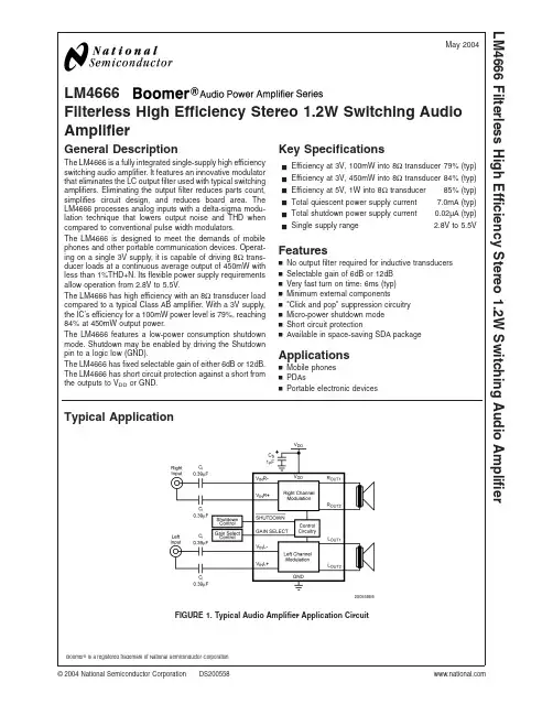
LM4666Filterless High Efficiency Stereo 1.2W Switching Audio AmplifierGeneral DescriptionThe LM4666is a fully integrated single-supply high efficiency switching audio amplifier.It features an innovative modulator that eliminates the LC output filter used with typical switching amplifiers.Eliminating the output filter reduces parts count,simplifies circuit design,and reduces board area.The LM4666processes analog inputs with a delta-sigma modu-lation technique that lowers output noise and THD when compared to conventional pulse width modulators.The LM4666is designed to meet the demands of mobile phones and other portable communication devices.Operat-ing on a single 3V supply,it is capable of driving 8Ωtrans-ducer loads at a continuous average output of 450mW with less than 1%THD+N.Its flexible power supply requirements allow operation from 2.8V to 5.5V.The LM4666has high efficiency with an 8Ωtransducer load compared to a typical Class AB amplifier.With a 3V supply,the IC’s efficiency for a 100mW power level is 79%,reaching 84%at 450mW output power.The LM4666features a low-power consumption shutdown mode.Shutdown may be enabled by driving the Shutdown pin to a logic low (GND).The LM4666has fixed selectable gain of either 6dB or 12dB.The LM4666has short circuit protection against a short from the outputs to V DD or GND.Key Specificationsj Efficiency at 3V,100mW into 8Ωtransducer 79%(typ)j Efficiency at 3V,450mW into 8Ωtransducer 84%(typ)j Efficiency at 5V,1W into 8Ωtransducer 85%(typ)j Total quiescent power supply current 7.0mA (typ)j Total shutdown power supply current 0.02µA (typ)j Single supply range2.8V to 5.5VFeaturesn No output filter required for inductive transducers n Selectable gain of 6dB or 12dB n Very fast turn on time:6ms (typ)n Minimum external componentsn "Click and pop"suppression circuitry n Micro-power shutdown mode n Short circuit protectionnAvailable in space-saving SDA packageApplicationsn Mobile phones n PDAsn Portable electronic devicesTypical ApplicationBoomer ®is a registered trademark of National Semiconductor Corporation.200558E6FIGURE 1.Typical Audio Amplifier Application CircuitMay 2004LM4666Filterless High Efficiency Stereo 1.2W Switching Audio Amplifier©2004National Semiconductor Corporation Connection DiagramsSDA Package200558I8Top ViewOrder Number LM4666SDA See NS Package Number SDA14ASDA Marking200558I9Top View Z —Plant Code XY —Date Code TT —Die Traceability L4666—LM4666L M 4666 2Absolute Maximum Ratings(Notes1,2) If Military/Aerospace specified devices are required, please contact the National Semiconductor Sales Office/ Distributors for availability and specifications.Supply Voltage(Note1) 6.0V Storage Temperature−65˚C to+150˚C Voltage at Any Input Pin V DD+0.3V≥V≥GND-0.3V Power Dissipation(Note3)Internally Limited ESD Susceptibility,pins4,7,11,14(Note4)1kV ESD Susceptibility,all other pins(Note4)2.0kV ESD Susceptibility(Note5)200VJunction Temperature(T J)150˚C Thermal ResistanceθJA(SDA)63˚C/W θJC(SDA)12˚C/W Soldering InformationSee AN-1112"microSMD Wafers Level Chip Scale Package."Operating Ratings(Notes1,2)Temperature RangeT MIN≤T A≤T MAX−40˚C≤T A≤85˚C Supply Voltage 2.8V≤V DD≤5.5VElectrical Characteristics VDD =5V(Notes1,2)The following specifications apply for V DD=5V and R L=15µH+8Ω+15µH unless otherwise specified.Limits apply for T A= 25˚C.Symbol Parameter ConditionsLM4666Units(Limits) Typical Limit(Note6)(Notes7,8)I DD Quiescent Power Supply Current V IN=0V,No LoadV IN=0V,R L=15µH+8Ω+15µH 1516mAmAI SD Shutdown Current V SD=GND(Note9)0.02µA V SDIH Shutdown Voltage Input High 1.2V V SDIL Shutdown Voltage Input Low 1.1V V GSIH Gain Select Input High 1.2V V GSIL Gain Select Input Low 1.1V A V Closed Loop Gain V Gain Select=V DD6dB A V Closed Loop Gain V Gain Select=GND12dB V OS Output Offset Voltage10mV T WU Wake-up Time6msP o Output Power THD=1%(max),f=1kHz,22kHz BW1.2WTHD+N Total Harmonic Distortion+Noise P O=100mW RMS/Channel,f IN=1kHz,22kHz BW,Both channels in phase0.65%X TALK Channel Separation P O=100mW RMS,f=1kHz57dBR IN Differential Input Resistance V Gain Select=V DD90kΩV Gain Select=GND60kΩPSRR Power Supply Rejection Ratio V Ripple=100mV RMS sine wave,f RIPPLE=217HzInputs terminated to AC GND60dBV Ripple=100mV RMS sine wave,f RIPPLE=217HzP OUT=10mW,1kHz65dBCMRR Common Mode Rejection Ratio V Ripple=100mV RMS,f Ripple=217Hz,Input referred48dBSNR Signal to Noise Ratio P O=1W RMS;A-Weighted Filter83dBe OUT Output Noise A-Weighted filter,V in=0V200µVLM46663Electrical Characteristics V DD =3V(Notes 1,2)The following specifications apply for V DD =3V and R L =15µH +8Ω+15µH unless otherwise specified.Limits apply for T A =25˚C.Symbol ParameterConditionsLM4666Units (Limits)Typical Limit (Note 6)(Notes 7,8)I DD Quiescent Power Supply Current V IN =0V,No LoadV IN =0V,R L =15µH +8Ω+15µH 6.57.010mA (max)I SD Shutdown CurrentV SD =GND (Note 9)0.02 2.0µA (max)V SDIH Shutdown Voltage Input High 1.0 1.4V (min)V SDIL Shutdown Voltage Input Low 0.80.4V (max)V GSIH Gain Select Input High 1.0 1.4V (min)V GSIL Gain Select Input Low 0.80.4V (max)A V Closed Loop Gain V Gain Select=V DD 6 5.256.75dB (min)dB (max)A V Closed Loop Gain V GainSelect=GND1211.2512.75dB (min)dB (max)V OS Output Offset Voltage 1035mV (max)T WU Wake-up Time 6msP oOutput PowerTHD =1%(max);f =1kHz,22kHz BW450400mW (min)THD+N Total Harmonic Distortion+Noise P O =100mW RMS /Channel,f IN =1kHz,22kHz BW,Both channels in phase 0.65%X TALK Channel Separation P O =100mW RMS ,f =1kHz 57dB R INDifferential Input ResistanceV Gain Select =V DD 90k ΩV GainSelect=GND60k ΩPSRR Power Supply Rejection RatioV ripple =100mV RMS sine wave,f RIPPLE =217Hz,Inputs terminated to AC GND 60dBV Ripple =100mV RMS sine wave,f RIPPLE =217Hz,P OUT =10mW,1kHz65dBCMRR Common Mode Rejection Ratio V Ripple =100mV RMS ,f Ripple =217Hz,Input referred 48dB SNR Signal to Noise Ratio P O =400mW RMS ,A-Weighted Filter 83dB e OUTOutput NoiseA-Weighted filter,V in =0V125µVNote 1:All voltages are measured with respect to the ground pin,unless otherwise specified.Note 2:Absolute Maximum Ratings indicate limits beyond which damage to the device may occur.Operating Ratings indicate conditions for which the device is functional,but do not guarantee specific performance limits.Electrical Characteristics state DC and AC electrical specifications under particular test conditions which guarantee specific performance limits.This assumes that the device is within the Operating Ratings.Specifications are not guaranteed for parameters where no limit is given,however,the typical value is a good indication of device performance.Note 3:The maximum power dissipation must be derated at elevated temperatures and is dictated by T JMAX ,θJA ,and the ambient temperature T A .The maximum allowable power dissipation is P DMAX =(T JMAX –T A )/θJA or the number given in Absolute Maximum Ratings,whichever is lower.For the LM4666,T JMAX =150˚C.The typical θJA is 63˚C/W and the typical θJC is 12˚C/W for the SDA package.Note 4:Human body model,100pF discharged through a 1.5k Ωresistor.Note 5:Machine Model,220pF –240pF discharged through all pins.Note 6:Typical specifications are specified at 25˚C and represent the parametric norm.Note 7:Tested limits are guaranteed to National’s AOQL (Average Outgoing Quality Level).Note 8:Datasheet min/max specification limits are guaranteed by design,test,or statistical analysis.Note 9:Shutdown current is measured in a normal room environment.Exposure to direct sunlight will increase I SD by a maximum of 2µA.The Shutdown pin should be driven as close as possible to GND for minimal shutdown current and to V DD for the best THD performance in PLAY mode.See the Application Information section under SHUTDOWN FUNCTION for more information.Note 10:The performance graphs were taken using the Audio Precision AUX–0025Switching Amplifier Measurement Filter in series with the LC filter on the demo board.L M 4666 4External Components Description(Figure 1)Components Functional Description1.C S Supply bypass capacitor which provides power supply filtering.Refer to the Power Supply Bypassing section for information concerning proper placement and selection of the supply bypass capacitor.2.C IInput AC coupling capacitor which blocks the DC voltage at the amplifier’s input terminals.Typical Performance Characteristics(Note 10)THD+N vs FrequencyV DD =5V,R L =15µH +8Ω+15µH P OUT =100mW/Channel,30kHz BWTHD+N vs FrequencyV DD =3V,R L =15µH +8Ω+15µH P OUT =100mW/Channel,30kHz BW2005582720055826THD+N vs FrequencyV DD =3V,R L =15µH +4Ω+15µH P OUT =100mW/Channel,30kHz BWTHD+N vs Output Power/Channel V DD =5V,R L =15µH +8Ω+15µHf =1kHz,22kHz BW2005582520055830LM46665Typical Performance Characteristics(Note 10)(Continued)THD+N vs Output Power/Channel V DD =3V,R L =15µH +4Ω+15µHf =1kHz,22kHz BWTHD+N vs Output Power/Channel V DD =3V,R L =15µH +8Ω+15µHf =1kHz,22kHz BW2005582820055829CMRR vs FrequencyV DD =5V,R L =15µH +8Ω+15µH V CM =100mV RMS Sine Wave,30kHz BW CMRR vs FrequencyV DD =3V,R L =15µH +8Ω+15µH V CM =100mV RMS Sine Wave,30kHz BW2005581120055810PSRR vs FrequencyV DD =5V,R L =15µH +8Ω+15µHV Ripple =100mV RMS Sine Wave,22kHz BW PSRR vs FrequencyV DD =3V,R L =15µH +8Ω+15µHV Ripple =100mV RMS Sine Wave,22kHz BW2005581920055818L M 4666 6Typical Performance Characteristics(Note10)(Continued)Efficiency and Power Dissipationvs Output PowerV DD=5V,R L=15µH+8Ω+15µH,f=1kHz,THD≤1%Efficiency and Power Dissipationvs Output PowerV DD=3V,R L=15µH+8Ω+15µH,f=1kHz,THD≤1%2005581420055813Efficiency and Power Dissipationvs Output PowerV DD=3V,R L=15µH+4Ω+15µH,f=1kHz,THD≤1%Gain Select ThresholdV DD=3V20055812200558H6Gain Select ThresholdV DD=5VGain Select Thresholdvs Supply VoltageR L=15µH+8Ω+15µH200558H120055815LM4666 7Typical Performance Characteristics(Note 10)(Continued)Output Power/Channel vs Supply VoltageR L =15µH +8Ω+15µH,f =1kHz22kHz BWOutput Power/Channel vs Supply VoltageR L =15µH +4Ω+15µH,f =1kHz22kHz BW2005581720055816Shutdown ThresholdV DD =5V Shutdown ThresholdV DD =3V2005582220055821Shutdown Threshold vs Supply Voltage R L =15µH +8Ω+15µH Supply Current vs Shutdown Voltage R L =15µH +8Ω+15µH2005582020055823L M 4666 8LM4666 Typical Performance Characteristics(Note10)(Continued)Supply Currentvs Supply VoltageR L=15µH+8Ω+15µH Array 200558249Application InformationGENERAL AMPLIFIER FUNCTIONThe output signals generated by the LM4666consist of two,BTL connected,output signals that pulse momentarily from near ground potential to V DD on each channel.The two outputs on a given channel can pulse independently with the exception that they both may never pulse simultaneously as this would result in zero volts across the BTL connected load.The minimum width of each pulse is approximately 160ns.However,pulses on the same output can occur se-quentially,in which case they are concatenated and appear as a single wider pulse to achieve an effective 100%duty cycle.This results in maximum audio output power for a given supply voltage and load impedance.The LM4666can achieve much higher efficiencies than class AB amplifiers while maintaining acceptable THD performance.The short (160ns)drive pulses emitted at the LM4666out-puts means that good efficiency can be obtained with mini-mal load inductance.The typical transducer load on an audio amplifier is quite reactive (inductive).For this reason,the load can act as it’s own filter,so to speak.This "filter-less"switching amplifier/transducer load combination is much more attractive economically due to savings in board space and external component cost by eliminating the need for a filter.POWER DISSIPATION AND EFFICIENCYIn general terms,efficiency is considered to be the ratio of useful work output divided by the total energy required to produce it with the difference being the power dissipated,typically,in the IC.The key here is “useful”work.For audio systems,the energy delivered in the audible bands is con-sidered useful including the distortion products of the input signal.Sub-sonic (DC)and super-sonic components (>22kHz)are not useful.The difference between the power flowing from the power supply and the audio band power being transduced is dissipated in the LM4666and in the transducer load.The amount of power dissipation in the LM4666is very low.This is because the ON resistance of the switches used to form the output waveforms is typically less than 0.25Ω.This leaves only the transducer load as a po-tential "sink"for the small excess of input power over audio band output power.The LM4666dissipates only a fraction of the excess power requiring no additional PCB area or cop-per plane to act as a heat sink.DIFFERENTIAL AMPLIFIER EXPLANATIONAs logic supply voltages continue to shrink,designers are increasingly turning to differential analog signal handling to preserve signal to noise ratios with restricted voltage swing.The LM4666is a fully differential amplifier that features differential input and output stages.A differential amplifier amplifies the difference between the two input signals.Tra-ditional audio power amplifiers have typically offered only single-ended inputs resulting in a 6dB reduction in signal to noise ratio relative to differential inputs.The LM4666also offers the possibility of DC input coupling which eliminates the two external AC coupling,DC blocking capacitors.The LM4666can be used,however,as a single ended input amplifier while still retaining it’s fully differential benefits.In fact,completely unrelated signals may be placed on the input pins.The LM4666simply amplifies the difference be-tween the signals.A major benefit of a differential amplifier isthe improved common mode rejection ratio (CMRR)over single input amplifiers.The common-mode rejection charac-teristic of the differential amplifier reduces sensitivity to ground offset related noise injection,especially important in high noise applications.PCB LAYOUT CONSIDERATIONSAs output power increases,interconnect resistance (PCB traces and wires)between the amplifier,load and power supply create a voltage drop.The voltage loss on the traces between the LM4666and the load results is lower output power and decreased efficiency.Higher trace resistance between the supply and the LM4666has the same effect as a poorly regulated supply,increase ripple on the supply line also reducing the peak output power.The effects of residual trace resistance increases as output current increases due to higher output power,decreased load impedance or both.To maintain the highest output voltage swing and corre-sponding peak output power,the PCB traces that connect the output pins to the load and the supply pins to the power supply should be as wide as possible to minimize trace resistance.The rising and falling edges are necessarily short in relation to the minimum pulse width (160ns),having approximately 2ns rise and fall times,typical,depending on parasitic output capacitance.The inductive nature of the transducer load can also result in overshoot on one or both edges,clamped by the parasitic diodes to GND and V DD in each case.From an EMI standpoint,this is an aggressive waveform that can radiate or conduct to other components in the system and cause interference.It is essential to keep the power and output traces short and well shielded if e of ground planes,beads,and micro-strip layout techniques are all useful in preventing unwanted interference.As the distance from the LM4666and the speakers increase the amount of EMI radiation will increase since the output wires or traces acting as antenna become more efficient with length.What is acceptable EMI is highly application specific.Ferrite chip inductors placed close to the LM4666may be needed to reduce EMI radiation.The value of the ferrite chip is very application specific.POWER SUPPLY BYPASSINGAs with any power amplifier,proper supply bypassing is critical for low noise performance and high power supply rejection ratio (PSRR).The capacitor (C S )location should be as close as possible to the LM4666.Typical applications employ a voltage regulator with a 10µF and a 0.1µF bypass capacitors that increase supply stability.These capacitors do not eliminate the need for bypassing on the supply pin of the LM4666.A 1µF tantalum capacitor is recommended.SHUTDOWN FUNCTIONIn order to reduce power consumption while not in use,the LM4666contains shutdown circuitry that reduces current draw to less than 0.01µA.The trigger point for shutdown is shown as a typical value in the Electrical Characteristics Tables and in the Shutdown Hysteresis Voltage graphs found in the Typical Performance Characteristics section.It is best to switch between ground and supply for minimum current usage while in the shutdown state.While the LM4666may be disabled with shutdown voltages in between ground and supply,the idle current will be greater than theL M 466610Application Information(Continued) typical value.Increased THD may also be observed with voltages less than V DD on the Shutdown pin when in PLAY mode.The LM4666has an internal resistor connected between GND and Shutdown pins.The purpose of this resistor is to eliminate any unwanted state changes when the Shutdown pin is floating.The LM4666will enter the shutdown state when the Shutdown pin is left floating or if not floating,when the shutdown voltage has crossed the threshold.To mini-mize the supply current while in the shutdown state,the Shutdown pin should be driven to GND or left floating.If the Shutdown pin is not driven to GND,the amount of additional resistor current due to the internal shutdown resistor can be found by Equation(1)below.(V SD-GND)/60kΩ(1)With only a0.5V difference,an additional8.3µA of currentwill be drawn while in the shutdown state.GAIN SELECTION FUNCTIONThe LM4666has fixed selectable gain to minimize externalcomponents,increase flexibility and simplify design.For adifferential gain of6dB,the Gain Select pin should be per-manently connected to V DD or driven to a logic high level.For a differential gain of12dB,the Gain Select pin should bepermanently connected to GND or driven to a logic low level.The gain of the LM4666can be switched while the amplifieris in PLAY mode driving a load with a signal without damageto the IC.The voltage on the Gain Select pin should beswitched quickly between GND(logic low)and V DD(logichigh)to eliminate any possible audible artifacts from appear-ing at the output.For typical threshold voltages for the GainSelect function,refer to the Gain Threshold Voltages graphin the Typical Performance Characteristics section.LM466611Application Information(Continued)CIRCUIT CONFIGURATIONS20055803FIGURE 2.Single-Ended input with low gain selection configuration20055802FIGURE 3.Differential input with low gain selection configurationL M 4666 12Application Information(Continued) REFERENCE DESIGN BOARD SCHEMATICIn addition to the minimal parts required for the application circuit,a measurement filter is provided on the evaluation circuit board so that conventional audio measurements can be conveniently made without additional equipment.This is a balanced input,grounded differential output low pass filter with a3dB frequency of approximately35kHz and an on board termination resistor of300Ω(see schematic).Note that the capacitive load elements are returned to ground. This is not optimal for common mode rejection purposes,but due to the independent pulse format at each output there is a significant amount of high frequency common mode com-ponent on the outputs.The grounded capacitive filter ele-ments attenuate this component at the board to reduce the high frequency CMRR requirement placed on the analysis instruments.Even with the grounded filter the audio signal is still differ-ential necessitating a differential input on any analysis instru-ment connected to it.Most lab instruments that feature BNC connectors on their inputs are NOT differential responding because the ring of the BNC is usually grounded.The commonly used Audio Precision analyzer is differential but its ability to accurately reject fast pulses of160ns width is questionable necessitating the on board measurement filter. When the signal needs to be single-ended,use an audio signal transformer to convert the differential output to a single ended output.Depending on the audio transformer’s characteristics,there may be some attenuation of the audio signal which needs to be taken into account for correct measurement of performance.Measurements made at the output of the measurement filter suffer attenuation relative to the primary,unfiltered outputs even at audio frequencies.This is due to the resistance of the inductors interacting with the termination resistor(300Ω) and is typically about-0.35dB(4%).In other words,the voltage levels and corresponding power levels indicated through the measurement filter are slightly lower than those that actually occur at the load placed on the unfiltered out-puts.This small loss in the filter for measurement gives a lower output power reading than what is really occurring on the unfiltered outputs and its load.The AUX-0025Switching Amplifier Measurement Filter from Audio Precision may be used instead of the on board mea-surement filter.The AUX-0025filter should be connected to the high current direct outputs on the evaluation board and in series with the measurement equipment.Attaching oscillo-scope probes on the outputs of the AUX-0025filter will display the audio waveforms.The AUX-0025filter may also be connected to the on board filter without any adverse effects.20055801FIGURE4.LM4666 13Application Information(Continued)LM4666SDA BOARD ARTWORKComposite ViewSilk Screen2005580520055808Top Layer Internal Layer 1,GND2005580920055806Internal Layer 2,V DDBottom Layer2005580720055804L M 4666 14Physical Dimensionsinches (millimeters)unless otherwise notedLLP PackageOrder NumberLM4666SD NS Package Number SDA14ALIFE SUPPORT POLICYNATIONAL’S PRODUCTS ARE NOT AUTHORIZED FOR USE AS CRITICAL COMPONENTS IN LIFE SUPPORT DEVICES OR SYSTEMS WITHOUT THE EXPRESS WRITTEN APPROVAL OF THE PRESIDENT AND GENERAL COUNSEL OF NATIONAL SEMICONDUCTOR CORPORATION.As used herein:1.Life support devices or systems are devices or systems which,(a)are intended for surgical implant into the body,or (b)support or sustain life,and whose failure to perform when properly used in accordance with instructions for use provided in the labeling,can be reasonably expected to result in a significant injury to the user. 2.A critical component is any component of a life support device or system whose failure to perform can be reasonably expected to cause the failure of the life support device or system,or to affect its safety or effectiveness.BANNED SUBSTANCE COMPLIANCENational Semiconductor certifies that the products and packing materials meet the provisions of the Customer Products Stewardship Specification (CSP-9-111C2)and the Banned Substances and Materials of Interest Specification (CSP-9-111S2)and contain no ‘‘Banned Substances’’as defined in CSP-9-111S2.National Semiconductor Americas Customer Support CenterEmail:new.feedback@ Tel:1-800-272-9959National SemiconductorEurope Customer Support CenterFax:+49(0)180-5308586Email:europe.support@Deutsch Tel:+49(0)6995086208English Tel:+44(0)8702402171Français Tel:+33(0)141918790National Semiconductor Asia Pacific Customer Support CenterEmail:ap.support@National SemiconductorJapan Customer Support Center Fax:81-3-5639-7507Email:jpn.feedback@ Tel:81-3-5639-7560LM4666Filterless High Efficiency Stereo 1.2W Switching Audio AmplifierNational does not assume any responsibility for use of any circuitry described,no circuit patent licenses are implied and National reserves the right at any time without notice to change said circuitry and specifications.。
General DescriptionThe MAX2560/MAX2566/MAX2572 evaluation kits (EV kits) simplify testing of the MAX2560/MAX2566/MAX2572. The EV kits provide 50ΩSMA connectors for all RF inputs, baseband inputs, and RF outputs. On-board VCOs are provided for the on-chip PLLs.The EV kits allow evaluation of the MAX2560/MAX2566/MAX2572s’ I/Q modulator, RF upconverter, IF and RF VGAs, IF and RF PLLs, 3-wire programmable interface,and power-management features.The MAX2560/MAX2566/MAX2572 support CDMA,TDMA, and EDGE modes for US PCS and cellular bands, as well as W-CDMA mode for UMTS band. The MAX2566/MAX2572 also support GSM-GPRS mode for all four bands.Features♦On-Board PCS and Cellular VCOs♦WCDMA, GSM900, DCS1800, GSM1900 Modes (MAX2566/MAX2572 EV Kits)♦50ΩSMA Connectors on All RF and Baseband Ports♦Low-Power Shutdown Mode♦EV-Kit Control Software Available at ♦SPI TM /QSPI TM /MICROWIRE TM CompatibleEvaluate: MAX2560/MAX2566/MAX2572MAX2560/MAX2566/MAX2572 Evaluation Kits________________________________________________________________Maxim Integrated Products 1MAX2560 Component ListOrdering Information19-3368; Rev 0; 7/04For pricing, delivery, and ordering information,please contact Maxim/Dallas Direct!at 1-888-629-4642, or visit Maxim’s website at .Component SuppliersSPI and QSPI are trademarks of Motorola, Inc.Microwire is a trademark of National Semiconductor Corp.E v a l u a t e : M A X 2560/M A X 2566/M A X 2572MAX2560/MAX2566/MAX2572 Evaluation Kits 2_______________________________________________________________________________________MAX2560 Component List (continued)Evaluate: MAX2560/MAX2566/MAX2572MAX2560/MAX2566/MAX2572 Evaluation Kits_______________________________________________________________________________________3MAX2560 Component List (continued)E v a l u a t e : M A X 2560/M A X 2566/M A X 2572MAX2560/MAX2566/MAX2572 Evaluation Kits 4_______________________________________________________________________________________Evaluate: MAX2560/MAX2566/MAX2572MAX2560/MAX2566/MAX2572 Evaluation Kits_______________________________________________________________________________________5MAX2566 Component List (continued)E v a l u a t e : M A X 2560/M A X 2566/M A X 2572MAX2560/MAX2566/MAX2572 Evaluation Kits 6_______________________________________________________________________________________MAX2566 Component List (continued)Evaluate: MAX2560/MAX2566/MAX2572MAX2560/MAX2566/MAX2572 Evaluation Kits_______________________________________________________________________________________7E v a l u a t e : M A X 2560/M A X 2566/M A X 2572MAX2560/MAX2566/MAX2572 Evaluation Kits 8_______________________________________________________________________________________Quick Start The MAX2560/MAX2566/MAX2572 EV kits are fully assembled and factory tested. Follow the instructions in the Connections and Setup section.Test Equipment Required This section lists the recommended test equipment to verify the operation of the MAX2560/MAX2566/ MAX2572. It is intended as a guide only, and substitu-tions may be possible.•One RF signal generator capable of delivering -5dBm of output power in the 1GHz to 3GHz frequency range (HP8648 or equivalent) for the external RF LO •An RF spectrum analyzer with optional digital modu-lation personality (Rohde & Schwarz FSEA30 or equivalent)• A power supply capable of providing 200mA at +5V • A power supply capable of providing 50mA at 6.8V • A power supply capable of providing -50mA at -3.2V •I/Q arbitrary waveform generator (Agilent E4433B or equivalent)•PC (486DX33 or better) with Windows TM95/98, 2000, NT 4.0 or later operating system and an available parallel port•INTF2300 interface board (supplied with EV kit)Connections and Setup This section provides step-by-step instructions for get-ting the EV kit up and running in CDMA, WCDMA, and GSM modes.1)Verify shunts JU6–JU22 and JU28–JU31 are in place.2)Connect the INTF2300 interface cable to the EV kit.Note:Pin 1 of the interface cable corresponds to the red wire. Pin 1 is designated in silkscreen on each of the PC boards.3)With the power supply turned off, connect a +5.0Vpower supply to the header labeled V5.0 (J31).Connect the power-supply ground to the header labeled GND (J5). (The MAX2560 requires two additional power supplies. Connect the +6.8V power supply to JU28, and connect the -3.2V to TP2. Connect the grounds to GND (J5) or GND (J20), or both.)4)Install and run the MAX2560/MAX2572 control soft-ware. The MAX2566 has its own control software.Software is available for download on the Maxim website at .5)With MAX2560/MAX2566/MAX2572 control softwareactive in the REG screen, set the SHDN box to 0 toplace the IC in shutdown mode.6)Turn on the power supplies.Cellular CDMA Mode Perform the following steps to evaluate the MAX2560 inthe cellular CDMA mode:1)Verify shunt JU24 is in the LOTDMA position.2)With MAX2560/MAX2566/MAX2572 control softwareactive in the REG screen, use Table 1 to set the oper-ating mode to cellular CDMA. Also, change the refer-ence frequency to 19.2MHz in the control software.3)Connect the I and Q outputs of the arbitrary wave-form generator to the I (J15) and Q (J16) ports. Setthe generator to reverse-channel CDMA settings.Set the output voltage level to 400mV PK.4)Connect RFL (J9) to the spectrum analyzer.Configure the spectrum analyzer to measure ACPRfor the reverse-channel CDMA. Set the center fre-quency to 836MHz with 50MHz span and a+10dBm reference level.5)Adjust the R6 (VGCIF) to obtain an output power of+8dBm after accounting for cable and connectorloss. The ACPR in 30kHz bandwidth at ±885kHzoffset should be -54dBc, and the ACPR in 30kHzbandwidth at ±1.98MHz offset should be -65dBc.PCS CDMA Mode Perform the following steps to evaluate the MAX2560 inthe PCS CDMA mode:1)Verify shunt JU24 is in the LOTDMA position.2)With MAX2560/MAX2566/MAX2572 control softwareactive in the REG screen, use Table 1 to set theoperating mode to PCS CDMA. Also, change the ref-erence frequency to 19.2MHz in the control software.3)Connect the I and Q outputs of the arbitrary wave-form generator to the I (J15) and Q (J16) ports. Setthe generator to reverse-channel CDMA settings.Set the output voltage level to 400mV PK.4)Connect RFH0 (J1) to the spectrum analyzer.Configure the spectrum analyzer to measure ACPRfor the reverse-channel CDMA. Set the center fre-quency to 1880MHz with 50MHz span and a+10dBm reference level.5)Adjust the R6 (VGCIF) to obtain an output power of+8dBm after accounting for cable and connectorloss. The ACPR in 30kHz bandwidth at ±1.25MHzoffset should be -54dBc, and the ACPR in 30kHzbandwidth at ±1.98MHz offset should be -65dBc. Evaluate: MAX2560/MAX2566/MAX2572MAX2560/MAX2566/MAX2572 Evaluation Kits _______________________________________________________________________________________9 Windows is a trademark of Microsoft.E v a l u a t e : M A X 2560/M A X 2566/M A X 2572WCDMA ModePerform the following steps to evaluate the MAX2566/MAX2572 in the WCDMA mode:1)Verify shunt JU24 is in the LOUMTS position.2)With MAX2560/MAX2566/MAX2572 control softwareactive in the REG screen, use Tables 2 and 3 to set the operating mode to WCDMA.3)Connect the I and Q outputs of the arbitrary wave-form generator to the I (J15) and Q (J16) ports. Set the generator to WCDMA settings. Verify 300mV peak baseband signal on Q+/Q- (JU2) and I+/I-(JU1), or 600mV peak-to-peak differential.4)The MAX2566 EV kit requires an external LO input.Apply an external LO 1565MHz at -10dBm to the LOH port.5)Connect RFH0 (J1) to the spectrum analyzer.Configure the spectrum analyzer to measure ACPR for the uplink WCDMA. Set the center frequency to 1950MHz with 50MHz span and a +10dBm refer-ence level.6)Adjust the R1 (VGCRF) and R6 (VGCIF) (only adjustVGCIF if VGS = 1) to obtain an output power of +8dBm after accounting for cable and connector loss.The ACPR in 3.84MHz bandwidth at ±5MHz offset should be -49dBc, and the ACPR in 3.84MHz band-width at ±10MHz offset should be -62dBc. Note that C112–C115 are disconnected for this measurement.GSM 900 ModePerform the following steps to evaluate the MAX2566/MAX2572 in the GSM 900 mode:1)Verify shunts JU23–JU26 and JU33 positions withTable 4.2)With MAX2560/MAX2566/MAX2572 control softwareactive in the REG screen, use Tables 2 and 3 to set the operating mode to GSM 900 mode.3)Connect the I and Q outputs of the arbitrary wave-form generator to the I (J15) and Q (J16) ports. Set the generator to GSM settings. Verify 300mV peak baseband signal on Q+/Q- (JU2) and I+/I- (JU1), or 600mV peak-to-peak differential.4)The MAX2566 EV kit requires an external LO input.Apply an external LO 1190MHz at -10dBm to the LOH port.5)Connect GSM (J3) to the spectrum analyzer.Configure the spectrum analyzer to measure spec-tral mask for the GSM signal. Set the center fre-quency to 900MHz with 50MHz span and a +10dBm reference level.MAX2560/MAX2566/MAX2572 Evaluation KitsDCS 1800 Mode Perform the following steps to evaluate the MAX2566/MAX2572 in the DCS 1800 mode:1)Verify shunts JU23–JU26 and JU33 positions withTable 4.2)With MAX2560/MAX2566/MAX2572 control softwareactive in the REG screen, use Tables 2 and 3 to set the operating mode to DCS 1800 mode.3)Connect the I and Q outputs of the arbitrary wave-form generator to the I (J15) and Q (J16) ports. Set the generator to GSM settings. Verify 300mV peak baseband signal on Q+/Q- (JU2) and I+/I- (JU1), or 600mV peak-to-peak differential.4)The MAX2566 EV kit requires an external LO input.Apply an external LO 1510MHz at -10dBm to the LOH port.5)Connect GSM (J33) to the spectrum analyzer.Configure the spectrum analyzer to measure spec-tral mask for the GSM signal. Set the center fre-quency to 1800MHz with 50MHz span and a +10dBm reference level.GSM 1900 Mode Perform the following steps to evaluate the MAX2566/MAX2572 in the GSM 1900 mode:1)Verify shunts JU23–JU26 and JU33 positions withTable 4.2)With MAX2560/MAX2566/MAX2572 control softwareactive in the REG screen, use Tables 2 and 3 to set the operating mode to GSM 1900 mode.3)Connect the I and Q outputs of the arbitrary wave-form generator to the I (J15) and Q (J16) ports. Setthe generator to GSM settings. Verify 300mV peakbaseband signal on Q+/Q- (JU2) and I+/I- (JU1), or600mV peak-to-peak differential.4)The MAX2566 EV kit requires an external LO input.Apply an external LO 1610MHz at -10dBm to theLOH port.5)Connect GSM (J33) to the spectrum analyzer.Configure the spectrum analyzer to measure spec-tral mask for the GSM signal. Set the center fre-quency to 1900MHz with a +10dBm reference level.Layout ConsiderationsThe MAX2560/MAX2566/MAX2572 EV kits can serve as guides for board layout. Keep PC board trace lengthsas short as possible to minimize parasitics. Also, keep decoupling capacitors as close to the IC as possiblewith a direct connection to the ground plane.INTF2300 SPI Interface BoardThe INTF2300 interface board is used to interface 3-wire SPI protocol from a PC’s parallel port to the EV kit.This board level translates 5V logic from the PC to VCCof the EV kit (typically, this is 2.85V logic). The INTF2300also provides buffering and EMI filtering. Its absolute maximum supply voltage is 4.6V, limited by the break-down of the buffer IC. The recommended operating supply voltage range is +2.7V to +3.6V.Evaluate: MAX2560/MAX2566/MAX2572MAX2560/MAX2566/MAX2572 Evaluation KitsE v a l u a t e : M A X 2560/M A X 2566/M A X 2572MAX2560/MAX2566/MAX2572 Evaluation KitsFigure 1. MAX2560 EV Kit Schematic (Sheet 1 of 3)MAX2560/MAX2566/MAX2572 Evaluation KitsEvaluate: MAX2560/MAX2566/MAX2572Figure 1. MAX2560 EV Kit Schematic (Sheet 2 of 3)E v a l u a t e : M A X 2560/M A X 2566/M A X 2572MAX2560/MAX2566/MAX2572 Evaluation KitsFigure 1. MAX2560 EV Kit Schematic (Sheet 3 of 3)MAX2560/MAX2566/MAX2572 Evaluation KitsEvaluate: MAX2560/MAX2566/MAX2572Figure 2. MAX2566 EV Kit Schematic (Sheet 1 of 3)E v a l u a t e : M A X 2560/M A X 2566/M A X 2572MAX2560/MAX2566/MAX2572 Evaluation KitsFigure 2. MAX2566 EV Kit Schematic (Sheet 2 of 3)MAX2560/MAX2566/MAX2572 Evaluation KitsEvaluate: MAX2560/MAX2566/MAX2572Figure 2. MAX2566 EV Kit Schematic (Sheet 3 of 3)E v a l u a t e : M A X 2560/M A X 2566/M A X 2572MAX2560/MAX2566/MAX2572 Evaluation KitsFigure 3. MAX2572 EV Kit Schematic (Sheet 1 of 3)MAX2560/MAX2566/MAX2572 Evaluation KitsEvaluate: MAX2560/MAX2566/MAX2572Figure 3. MAX2572 EV Kit Schematic (Sheet 2 of 3)E v a l u a t e : M A X 2560/M A X 2566/M A X 2572MAX2560/MAX2566/MAX2572 Evaluation KitsFigure 3. MAX2572 EV Kit Schematic (Sheet 3 of 3)Evaluate: MAX2560/MAX2566/MAX2572MAX2560/MAX2566/MAX2572 Evaluation Kits ______________________________________________________________________________________21Figure 5. MAX256_/MAX257_ EV Kit Component Placement Guide—Solder SideFigure 4. MAX256_/MAX257_ EV Kit Component PlacementGuide—Component SideFigure 7. MAX256_/MAX257_ EV Kit PC Board Layout—Ground PlaneFigure 6. MAX256_/MAX257_ EV Kit PC Board Layout—Component SideE v a l u a t e : M A X 2560/M A X 2566/M A X 2572MAX2560/MAX2566/MAX2572 Evaluation Kits Maxim cannot assume responsibility for use of any circuitry other than circuitry entirely embodied in a Maxim product. No circuit patent licenses are implied. Maxim reserves the right to change the circuitry and specifications without notice at any time.22____________________Maxim Integrated Products, 120 San Gabriel Drive, Sunnyvale, CA 94086 408-737-7600©2004 Maxim Integrated Products Printed USA is a registered trademark of Maxim Integrated Products.Figure 8. MAX256_/MAX257_ EV Kit PC Board Layout—Inner Layer Figure 9. MAX256_/MAX257_ EV Kit PC Board Layout—SolderSide。
Eaton 066167Eaton Moeller® series EMT6 Thermistor overload relay for machine protection, 24-240V50/60HZ/DCEspecificaciones generalesEaton Moeller® series EMT6 Thermistor overload relay0661674015080661672103 mm 83 mm 23 mm 0.132 kg UL File No.: E29184 UL EN 55011CSA Class No.: 3211-03 IEC/EN 60947 CE UL 508IEC/EN 61000-4-2 CSAUL Category Control No.: NKCR IEC/EN 60947-8 CSA-C22.2 No. 14 CSA File No.: 12528 VDE 0660 IEC/EN 61000-4-3EMT6-DBProduct NameCatalog NumberEANProduct Length/Depth Product Height Product Width Product Weight CertificationsModel CodeScrew connectionManual or remote resettingNotifications of mains and faults via LED display Test function via separate buttonExternal reset possibleManual reset0 °C0 °C IP20As requiredIII3EMT6 thermistor overload relay for machine protectionFinger and back-of-hand proof, Protection against direct contact when actuated from front (EN 50274)6000 V AC4000 V AC250 V AC, Between the contacts and power supply, According to EN 61140250 V AC, Between the contacts, According to EN 6114010 g, Mechanical, according to IEC/EN 60068-2-27, Half-sinusoidal shock 10 msAC/DC-25 °C 60 °C 25 °C 45 °C 8 kV1 kV, Signal cable2 kV, Supply cableAccording to IEC/EN 61000-4-4 6 kVElectric connection typeFunctionsTemperature measuring range - min Temperature measuring range - max Degree of protectionMounting positionOvervoltage categoryPollution degreeProduct categoryProtectionRated impulse withstand voltage (Uimp) Safe isolationShock resistanceVoltage typeAmbient operating temperature - minAmbient operating temperature - maxAmbient operating temperature (enclosed) - min Ambient operating temperature (enclosed) - max Air dischargeBurst impulse Contact discharge Electromagnetic fields45 °C85 °CDamp heat, cyclic, to IEC 60068-2-30 Damp heat, constant, to IEC 60068-2-7810 V/m at 80 - 1000 MHz (according to IEC EN 61000-4-3) 3 V/m at 1.4 - 2 GHz (according to IEC EN 61000-4-3)1 V/m at 2.0 - 2.7 GHz (according to IEC EN 61000-4-3)10 V (according to IEC/EN 61000-4-6)Class B (EN 55011)According to IEC/EN 61000-4-5, power pulses (Surge), EMC 2 kV, symmetrical, power pulses (Surge), EMC4 kV, asymmetrical, power pulses (Surge), EMC1 x (0.5 - 2.5) mm², solid1 x (0.5 - 2.5) mm², flexible with ferrule2 x (0.5 - 1.5) mm², flexible with ferrule2 x (0.5 - 1.5) mm², solid20 - 14 AWG, solid or strandedM3.5, Terminal screw1 x 6 mm, Terminal screw, Standard screwdriver 2, Terminal screw, Pozidriv screwdriver1.2 Nm, Screw terminals 6 A0.85 - 1.1 V x Uₑ2 W at DC3.5 VA at AC24 V240 V24 V240 V24 V240 V400 V3 A at AC-14, 400 V (NC)3 A at AC-14, 380 V 400 V 415 V (NC) 3 A at AC-15, 220 V 230 V 240 V (NO)Ambient storage temperature - minAmbient storage temperature - max Climatic proofing Immunity to line-conducted interference Radio interference classSurge ratingTerminal capacityScrew size Screwdriver size Tightening torque Conventional thermal current ith of auxiliary contacts (1-pole, open)Pick-up voltagePower consumptionRated control supply voltage (Us) at AC, 50 Hz - minRated control supply voltage (Us) at AC, 50 Hz - maxRated control supply voltage (Us) at AC, 60 Hz - minRated control supply voltage (Us) at AC, 60 Hz - maxRated control supply voltage (Us) at DC - minRated control supply voltage (Us) at DC - maxRated insulation voltage (Ui)Rated operational current (Ie)3 A at AC-15, 220 V 230 V 240 V (NC) 3 A at AC-15, 220 V 230 V 240 V 3 A at AC-14, 300 V (NC) 1 A at AC-15, 300 V (NC) 3 A at AC-14, 300 V (NO)1 A at AC-15, 380 V 400 V 415 V (NO) 3 A at AC-14, 380 V 400 V 415 V (NO) 1 A at AC-15, 300 V (NO)1 A at AC-15, 380 V 400 V 415 V (NC)240 V1600 ΩMax. 6 A gG/gL, Fuse, Contacts3600 Ω600 V110 W0 W 0 W 0 A0.8 W eaton-tripping-emt6-thermistor-overload-relay-characteristic-curve-002.epseaton-tripping-emt6-thermistor-overload-relay-characteristic-curve.eps eaton-tripping-devices-relay-emt6-thermistor-overload-relay-dimensions.epseaton-tripping-thermistor-relay-emt6-dimensions.epseaton-tripping-devices-relay-emt6-thermistor-overload-relay-3d-drawing-002.eps DA-CE-ETN.EMT6-DB eaton-tripping-devices-emt6-thermistor-overload-relay-wiring-diagram.epsRated operational voltage (Ue) - max Reset resistance Short-circuit protection rating Trip resistance Voltage rating - max Number of contacts (change-over contacts)Number of contacts (normally closed contacts)Number of contacts (normally open contacts)Equipment heat dissipation, current-dependent PvidHeat dissipation capacity PdissHeat dissipation per pole, current-dependent PvidRated operational current for specified heat dissipation (In)Static heat dissipation, non-current-dependent Pvs Characteristic curveDibujoseCAD model Esquemas eléctricosEaton Corporation plc Eaton House30 Pembroke Road Dublin 4, Ireland © 2023 Eaton. All Rights Reserved. Eaton is a registered trademark.All other trademarks areproperty of their respectiveowners./socialmediaeaton-tripping-devices-auto-mode-emt6-thermistor-overload-relay-wiring-diagram.eps EMR6 - EMT6 - ETR4 brochure DA-DC-00003562.pdf DA-DC-00003971.pdf eaton-emt6-thermistor-motor-protection-relays-instruction-leaflet-il121016zu.pdf DA-CD-emt6_db DA-CS-emt6_dbFolletosInformes de certificación Instrucciones de montajemCAD model。
July 2000ML4664*/ML4669*10BASE-FL to 10BASE-T ConverterGENERAL DESCRIPTIONThe fully pin-compatible ML4664/ML4669 pair provide conversion from 10BASE-T copper media to 10BASE-FL fiber media in a single chip. They are compliant with Ethernet IEEE 802.3 10BASE-T and 10BASE-FL standards.The ML4664/69 uses a single 5V supply, and requires no crystal or clock.Their 10BASE-FL transmitter offers a current drive output that directly drives a fiber optic LED transmitter. Their receiver offers a highly stable fiber optic data quantizer capable of accepting input signals as low as 2mV P-P with a 55dB dynamic range.The 10BASE-T portion of the pair contains current driven transmitter outputs that offer superior performancebecause their switching is highly symmetric, resulting in lowered RFI noise and jitter. By changing one external resistor the pair easily interfaces to 100W unshielded twisted pair, 150W shielded twisted pair, or a range of other characteristic impedances.The ML4664 does not pass along disconnect information,while the ML4669 does. A loss of light at the optical inputs does not stop link pulses from being sent at the twisted pair transmitter in the ML4664, but in the ML4669 the link pulses stop. Also, a loss of link at the twisted pair inputs will not stop the optical transmitter from sending idle in the ML4664, but the ML4669 stopssending idle. * Some Packages Are ObsoleteFEATURESs Full duplex operations Five network status LED outputs sIndustrial temperature option10BASE-FL FEATURES:sHighly stable data quantizer with 55dB input dynamic ranges Input sensitivity as low as 2mV P-PsUp to 100mA maximum current driven fiber optic LED output for accurate launch power (PLCC package)10BASE-T FEATURES:s Current driven output for low RFI noise and low jitter sDrives 100W unshielded or 150W shielded twisted pairs Polarity detect status pin capable of driving an LED s Automatic polarity correction s On-chip link test with enable/disable option BLOCK DIAGRAMOPINOPOUT OPVCC元器件交易网元器件交易网ML4664/ML4669PINNAMEFUNCTION1(29)C TIMERA capacitor from this pin to V CCdetermines the Link Monitor response time.2(30)LTFLink Test Fail. Active high. Normally this pin is low, indicating that the link is operational. If the link goes down resulting from the absence of link pulses or frames being received, the chip will go into the Link Test Fail state and bring LTF high.When the ML4664 is in the link test fail state, the optical and twisted pair transmitters are disabled from sending data. However, the optical transmitter does send an idle signal, and link pulses are sent at the twisted pair transmitter. When the ML4669 is in link test fail state, the optical and twisted pair transmitters are disabled from sending data. Also, the optical transmitter will not send an idle signal. However, link pulses may be sent at the twisted pair transmitter,depending on the optical inputs. See Table 1.This pin may be grounded to disable Link Test. In this mode no link pulses are sent and the link will not fail if no link pulses are received. If this pin is not used as an LED driver, and is not grounded, a 2k W 5% resistor should be connected between this pin and V CC .3(31)TPLEDIndicates that reception is taking place on the TPINP , TPINN pair. Active low LED driver, open collector. It is extended 16ms for visibility.Optionally, this pin may be grounded to disable the optical output. If this pin is not used as an LED driver and is not grounded, a 2k W , 5% resistor should be connected between TPLED and V CC .4(32)TPINP Twisted Pair receive data input.5(1)TPINNWhen this signal exceeds the receive squelch requirements the receive data is buffered and sent to the Rx± outputs.6(3)V CC 5V input14(12)PIN DESCRIPTION (Pin Number in Parentheses is for TQFP Version)PINNAMEFUNCTION7(4)TxCAP0An external capacitor of 680pF is 8(5)TxCAP1tied between these two pins to set the pulse width for the pre-equalization on the twisted pair transmitter. If these two pins areshorted together, no pre-equalization occurs. If the ML4664/ML4669 is driving only a short cable, or board traces, these pins may be shorted.9(6)GND Ground reference20(18)10(7)TPOUTN Pre-equalized differential balanced 11(8)TPOUTP current driven output. These outputsare connected to a balanced transmit output filter which drives the twisted pair cable through pulse transformers.The output current is set with an external resistor connected to RTSET allowing the chip to drive 100W unshielded , 150W shielded twisted pair cables or a range of other characteristic impedances.12(10)POLDISReceive Polarity status. Active low LED Driver, open collector output.Indicates the polarity of the receive twisted pair regardless of auto polarity correction. When low, receive polarity is reversed. When high, receive polarity is correct. This pin may be grounded to disable the polarity circuit. If this pin is not used as an LED driver, and is not grounded, a 2k W , 5% resistor should be connected between this pin and V CC .13(11)RTSETTP When using 100W unshielded twistedpair, a 220W resistor is tied between this pin and V CC . When using 150W shielded twisted pair, a 330W resistor is tied between this pin and V CC .15(13)RRSETA 1% 61.9k W resistor tied from this pin to V CC is used for internal biasing.16(14)RTSETOP Sets the current driven output of thetransmitter. A 115W resistor should be tied between this pin and V CC .元器件交易网ML4664/ML4669PINNAMEFUNCTION22(21)V REF A 2.5V reference with respect to GND 23(22)V THADJ This input pin sets the link monitor threshold24(23)AGND Analog Filtered Ground25(24)OPINNThis input pin should be capacitively coupled to filtered AV CC . The input resistance is approximately 1.3k W .26(25)OPINPThis input pin should be capacitively coupled to the input source. The input resistance is approximately 1.3k W .27(26)AV CC Analog Filtered 5V28(28)OPLEDIndicates reception is taking place on the OPINP , OPINN pair. Active low LED driver, open collector. It isextended 16ms for usability. This pin may be grounded to disable thetwisted pair outputs. If this pin is not used as an LED driver, and is not grounded, a 2k W , 5% resistor should be connected between this pin and V CC .PINNAMEFUNCTION17(15)LMONLink Monitor “Low Light” LED status output. Pulled low when voltage on the OPINP , OPINN inputs exceed min threshold set by V THADJ , and there are transitions on OPINP , OPINN indicating an idle signal or activedata. If the voltage on OPINP,OPINN inputs falls below the minimum threshold or transitions cease onOPINP , OPINN, LMON will go high.Active low LED driver, open collector.In the low light state, optical and twisted pair transmitters are disabled from sending data. The opticaltransmitter of the ML4664 does send an idle signal, and link pulses are sent at the twisted pair transmitter. For the ML4669, the twisted pair transmitter will not send link pulses, the optical transmitter may send an idle signal,depending on inputs. See Table 1.18(16)OPVCC 5V supply for fiber optic LED driver19(17)OPOUT Fiber optic LED driver output 21(20)V DCAn external capacitor on this pin integrates an error signal which nulls the offset of the input amplifier. If the DC feedback loop is not being used,this pin should be connected to V REF .PIN DESCRIPTION (Continued)元器件交易网ML4664/ML4669ABSOLUTE MAXIMUM RATINGSAbsolute maximum ratings are those values beyond which the device could be permanently damaged.Absolute maximum ratings are stress ratings only and functional device operation is not implied.Power Supply Voltage RangeV CC ...................................................................GND –0.3 to 6V Input Voltage Range: Digital Inputs(SQEN, LBDIS).......................GND –0.3 to V CC +0.3V Tx+, Tx–, V IN +, V IN –..............GND –0.3 to V CC +0.3V Junction Temperature.............................................150°C Storage Temperature................................–65°C to 150°C Lead Temperature (Soldering)................................260°CELECTRICAL CHARACTERISTICSUnless otherwise specified, T A = Operating Temperature Range, V CC = OPV CC = AV CC = 5V ± 5% (Note 1)SYMBOL PARAMETERCONDITIONSMIN TYP MAX UNITS I CC Power Supply Current RTSETOP = 115W140mA While Transmitting V REFReference VoltageC Suffix 2.30 2.60V I Suffix2.25 2.67V V OL LED Drivers: V OLR L = 300 for OPLED, TPLED, 1.5 3.5V POLLED LTF, and LMONI OPOUTOP Transmit Peak Output CurrentRTSETOP = 115 (Note 2) C Suffix475257mA I Suffix4658.5mA I TPOUT TP Transmit Peak Output Current RTSETTP = 22042mAV TPSQ TP Receive Squelch Voltage 300450585mV P-P H TP TP Receive Squelch Hysteresis 50%V TPIN TP Receive Input Voltage 3003100mV P-P R TPIN TP Receive Input Resistance 4k WV OPTH OP Receive Input Threshold V THADJ = V REF567mV P-P VoltageH OP OP Receive Input Threshold 20%HysteresisV OPIN OP Receive Input Voltage 21600mV P-P R OPIN OP Receive Input Resistance 0.81.32.0k W V OPCM OP Receive Common Mode 1.65V Voltage A V Amplifier Gain 100V/V V OFF Input Offset V DC = V REF (DC Loop Inactive)3mV V N Input Referred Noise 50MHz Bandwidth 25µVI THInput Bias Current at V THADJV THADJ = V REF–200200µAThermal Resistance (q JA )PLCC ...............................................................68°C/W TQFP ...............................................................80ºC/WOPERATING CONDITIONSTemperature RangeML4664/ML4669CX..................................0°C to 70°C ML4664/ML4669IQ ...............................–40°C to 85°C Supply Voltage (V CC ).........................................5V ± 5%LED on Current ......................................................10mA RRSET ........................................................61.9k W ± 1%RTSETOP.......................................................115W ± 1%RTSETTP........................................................220W ± 1%元器件交易网元器件交易网ML4664/ML4669ELECTRICAL CHARACTERISTICS (Continued)SYMBOL PARAMETER CONDITIONS MIN TYP MAX UNITS OP TO TP (SEE FIGURE 1)t TPODY Twisted Pair Start-up Delay500ns t TPSDY Twisted Pair Steady State Delay35ns t TPSPW Twisted Pair Turn Off Pulse Width180nst PS Twisted Pair Jitter±3.5ns TP TO OP (SEE FIGURE 2)t OPODY Optical Transmit Start-up Delay500ns t OPSDY Steady State Delay15ns t OPDI Turn Off Width from Data to Idle4002100ns 1/t IDF Idle Frequency0.85 1.25MHz P IDC Idle Duty Cycle4555%t OPJ Jitter into 31W Load±1.5ns OPTICAL LINK VERIFICATION (SEE FIGURES 3-5)t OLL No Light (No Transitions) toLMON High310µs t OLM Low Light (Below Threshold) toLMON High50100200µs t OLO Light On (Above Threshold, Transitions<3µs) to LMON Low0.250.50.75s TWISTED PAIR LINK VERIFICATION (SEE FIGURE 6)t LT Link Loss Time50150ms t LTMIN Link Time Minimum27ms t LTMAX Link Time Maximum25150ms LINK PULSE TRANSMIT (SEE FIGURE 7)t LPRR Link Pulse Rep Rate81624ms t LPW Link Pulse Width85120200ns LED TIMING (SEE FIGURE 8)t LED LED on Time81632msNote 1:Limits are guaranteed by 100% testing, sampling, or correlation with worst-case test conditions.Note 2:The output current may be increased to 100mA by changing the RTSETOP resistor for the CQ (PLCC) package option only. See equation (1) on page 9. The increased current option is not available for the CH (TQFP) package option.元器件交易网元器件交易网ML4664/ML4669 SYSTEM DESCRIPTIONOPTICAL TRANSMISSIONThe optical transmit function consists of detecting thepresence of data from the TP inputs TPINP and TPINN anddriving that data onto the fiber optic LED transmitter. Apositive signal on the TPINP lead relative to the TPINNlead will result in no current, hence the fiber optic LED isin a low light condition. When TPINP is more negativethan TPINN, the ML4664/ML4669 will sink current intothe chip and the fiber optic LED will light up.Before data will be transmitted onto the fiber optic cableit must exceed the squelch requirements. The TP inputs,squelch circuit serves the function of preventing any noisefrom being transmitted onto the fiber.FIBER OPTIC LED DRIVERThe output stage of the transmitter is a current modeswitch which develops the output light by sinking currentthrough the LED into the OPOUT pin. Once the currentrequirement for the LED is determined, the RTSETOPresistor is selected. The following equation is used toselect the correct RTSETOP resistor:RTSETOP=52mAI OUT´115W(1)The ML4664/ML4669 optical transmitter (in the PLCC package only) is capable of driving up to 100mA maximum which requires resistor RSTETOP to equal 60W. (This option is only available with the PLCC package) The transmitter enters the idle state when it detects start of idle on TPINP and TPINN input pins. After detecting the start of idle the transmitter switches to a 1MHz output idle signal.The output current is switched through the OPOUT pin during the on cycle and the OPVCC pin during the off cycle. Since the sum of the current in these two pins is constant, OPVCC should be connected as close as possible to the V CC connection for the LED.TP SQUELCHThe twisted pair receive data is transformer coupled and low pass filtered before it is fed into the input pins TPINP and TPINN. The input is differential with the common mode voltage internally set. At the start of packet reception from the twisted pair link, no more than 5 bits are received from the twisted pair cable and not transmitted. The first bit sent at the optical transmitter may contain phase violations or invalid data, but all subsequent bits are valid.The TP squelch will reject the following signals on the TPINP and TPINN inputs:1.All signals that produce a peak magnitude lessthan 300mV (450mV typical).2. All continuous sinusoidal signals of amplitude lessthan 6.2V P–P and frequency less than 2MHz.3.All single sinusoidal cycles of amplitude less than6.2V P–P and either polarity, where the frequency isbetween 2MHz and 15MHz. For a period of 4 BTbefore and after this single cycle, the signal willconform to (1) above.4.All sinusoidal cycles gated by a 100ns pulse gate ofamplitude less than 6.2V P–P and either polarity, where the sinusoidal frequency is between 2MHz and30MHz. The off time of the pulse gate on thesinusoidal signal shall be at least 400ns.The first three receive squelch criteria are required to conform to the 10BASE-T standard. The fourth receive squelch criteria exceeds the 10BASE-T requirements and enhances performance. The fourth squelch criteria prevents a false unsquelch caused by cross talk or noise typically found coupling from the phone lines onto the receive twisted pair.After the TP inputs are unsquelched, the detection threshold is lowered to 225mV. Upon passing the TP squelch requirements the receive data passes to the LED Driver. The addition of jitter through the TP to OP path is no more than ±1.5ns.While in the unsquelch state, the TP squelch circuit looks for the start of idle signal at the end of the packet. When start of idle is detected, TP squelch is turned on again. The proper start of idle occurs when the input signal remains above 300mV for 160ns.LINK TEST FUNCTIONTransmission — Whenever data is not being delivered to the twisted pair link, the idle signal is applied. The idle signal is a sequence of Link Pulses separated by a 16ms period of silence. The idle signal starts with a period of silence after a packet transmission ends. The link test pulse is a single high pulse with the same amplitude requirements as the data signal.Reception — The transceiver monitors the receive twisted pair input for packet and link pulse activity. If neither a packet nor a link test pulse is received for 50 to 150ms, the transceiver enters the Link Test Fail state and inhibits transmission and reception. Link pulses received with the wrong polarity will be ignored and cause the chip to go into link test fail.When a packet, or five consecutive link test pulses is received from the twisted pair input, the transceiver will exit the Link Test Fail state upon transmit and receive data being idle, and re-enable transmission and reception.元器件交易网ML4664/ML4669Link test pulses that do not occur within at most 25 to 150ms of each other are not considered consecutive.In addition, detected pulses that occur within a time between 2 to 7ms of a previous pulse will be considered as noise by the link test circuitry, and will reset the count of consecutive link pulses to zero.If the ML4664 enters the link test fail state, both link pulses at the twisted pair transmitter, and idle at theoptical transmitter will continue to be sent. Data will not be sent at either transmitter.If the ML4669 enters the link test fail state, idle will not be sent at the optical transmitter. Data will not be sent at either transmitter. However, link pulses may still be sent at the twisted pair transmitter, depending on the optical inputs. See Table 1.POLARLITY CIRCUITRYThe ML4664/ML4669 offers automatic polarity correction.The POLDIS pin is used to report the status of the receive pair polarity. This pin is high when the polarity is correct,and low when the polarity is reversed. If this pin is grounded, the polarity correction circuit is disabled.Polarity Detection — The internal circuitry uses the start of idle signal to determine the receive polarity. With the correct receive polarity, the Start of Idle signal (the end of the frame) will remain above 300mV for more than 160ns. If the polarity is reversed, the Start of Idle signal will end with a negative voltage.The POLDIS status pin is updated only when fourconsecutive frames are received with the same Start of Idle polarity. In the case where the part is powered up with the receive polarity reversed and no frames are received, the part will go into link test fail withoutreflecting a reverse polarity condition. If five consecutive revised link pulses are then received, the polarity will reverse and the device will come out of Link Test Fail.TP TRANSMISSIONThe TP transmit function consists of detecting thepresence of data from the OP inputs, OPINP and OPINN and driving that data onto the transmit twisted pair(TPOUTP , TPOUTN). A positive signal on the OPINP lead relative to the OPINN lead will result in a positive signal on the TPOUTP lead of the chip with respect to the TPOUTN lead.Before data will be transmitted onto the twisted pair from the OP inputs, it must exceed the squelch requirements for the OP inputs. The OP squelch circuit serves the function of preventing any noise from being transmitted onto the twisted pair.The output stage of the transmitter is a current mode switch which develops the output voltage by driving current through the terminating resistor and the output filter. The transmitter employs a center tap 2:1 transformer where the center tap is tied to V CC (+5V). While one pin of the transmit pair (TPOUTP , TPOUTN) is pulled low, the other pin floats. The output pins to the twisted pair wires,Figure 9. Transmit Pre-Equalization WaveformBINARY TxTP+TxTP–OUTPUT AFTER TRANSMIT FILTERINPUT INTO RECEIVER011100110SYSTEM DESCRIPTION (Continued)元器件交易网TPOUTP and TPOUTN, can drive a 100W, 150W load, or a variety of impedances that are characteristic of the twisted pair wire. RTSETTP selects the current into the TPOUTP, TPOUTN pins. This current along with the characteristic impedance of the cable determines the output voltage.Once the characteristic impedance of the twisted pair is determined, one must select the appropriate RTSETTP resistor as well as match the terminating impedances of the transmit and receive filter. The RTSETTP resistor can be selected as follows:RTSETTPR L=100220W(2)Where R L is the characteristic impedance of the twisted pair cable.The transmitter incorporates a pre-equalization circuit for driving the twisted pair line. Pre-equalization compensates for the amplitude and phase distortion introduced by the twisted pair cable. The twisted pair line will attenuate the 10MHz signal more than the 5MHz signal. Therefore pre-equalization insures that both the 5 and 10MHz components will be roughly the same amplitude at the far end receiver.The pre-equalization circuit reduces the current output when a 5MHz bit is being transmitted. After 50ns of a5MHz bit, the current level is reduced to approximately 2/3 of its peak for the remaining 50ns. Figure 9 illustrates the pre-equalization.An on-chip one-shot determines the pulse width of the pre-equalized transmit signal. This requires an external capacitor connected to pins TxCAP0 and TxCAP1. The proper value for this one-shot is 680pF. Pre-equalization can be disabled by shorting TxCAP0 and TxCAP1 together.The transmitter enters the idle state when it detects start of idle on OPINP and OPINN input pins. The transmitter maintains a minimum differential output voltage of at least 450mV for 250ns after the last low to high transition. The driver differential output voltage will then be within 50mV of 0V within 45 bit times.OP SQUELCHThe input to the optical receiver comes from a fiber optic pre-amp. At the start of packet reception no more than 2.7 bits are received from the fiber cable and not transmitted onto the TP outputs. The receive squelch will reject frequencies lower than 2.51MHz.While in the unsquelch state, the receive squelch circuit looks for the start of idle signal at the end of the packet. Start of idle occurs when the input signal remains idle for more than 160ns. When start of idle is detected, the receive squelch circuit returns to the squelch state and the start of idle signal is output on the twisted pair outputs TPOUTP, TPOUTN.INPUT AMPLIFIERThe OPINP, OPINN input signal is fed into a limiting amplifier with a gain of about 100 and input resistance of 1.3k W. Maximum sensitivity is achieved through the use of a DC restoration feedback loop and AC coupling the input. When AC coupled, the input DC bias voltage is set by an on-chip network at about 1.7V. These coupling capacitors, in conjunction with the input impedance of the amplifier, establish a high pass filter with 3dB corner frequency, f L, at:f=12CL p 1300(3)Since the amplifier has a differential input, two capacitors of equal value are required. If the signal driving the input is single ended, one of the coupling capacitors can be tied to AV CC.The internal amplifier has a lowpass filter built-in to band limit the input signal which in turn will improve the signal to noise ratio.Although the input is AC coupled, the offset voltage within the amplifier will be present at the amplifier’s output. In order to reduce this error a DC feedback loop is incorporated. This negative feedback loop nulls the offset voltage, forcing V OS to be zero. Although the capacitor on V DC is non-critical, the pole it creates can effect the stability of the feedback loop. To avoid stability problems, the value of this capacitor should be at least 10 times larger than the input coupling capacitors.The comparator is a high-speed differential zero crossing detector that slices and accurately digitizes the receive signal. The output of the comparator is fed into the receive squelch circuit.SYSTEM DESCRIPTION (Continued)1112OPTICAL LINK DETECT CIRCUIT AND LOW LIGHTThe link detect circuit monitors the input signal and determines when the input falls below a preset voltage level. When the input falls below a preset voltage, the ML4664/ML4669 goes into the Low Light state. In the Low Light state the TP transmitter is disabled, but continues sending link pulses, the receiver is disabled, and the LMON LED pin goes to high shutting off the LMON LED. To return to the Link Pass state, the optical receiver power must be 20% higher than the shut-off state. This built-in hysteresis adds stability to the Link Monitor circuit. Once the receiver power threshold is exceeded, the ML4664/ML4669 waits 250ms to 750ms, then checks to see that no data is being received before re-enabling the transmitter, and receiver, and lighting up the LMON LED.When the ML4664 is in the low light state, both the link pulses at the twisted pair transmitter and idle at the optical transmitter continue to be sent. However, when the ML4669 is in the low light state, link pulses are not sent at the twisted pair transmitter. Data is not sent at either transmitter. An idle signal may be sent at the optical transmitter, depending on the twisted pair inputs. See Table 1.The V THADJ pin is used to adjust the sensitivity of the receiver. The ML4664/ML4669 is capable of exceeding the 10BASE-FL specifications for sensitivity. The sensitivity is dependent on the layout of the PC board. A good low noise layout will exceed the 10BASE-FL specifications, while a poor layout will fail to meet the sensitivity and BER spec.The threshold generator shifts the reference voltage atV THADJ through a circuit which has a temperature coefficient matching that of the limiting amplifier. The relationship between the V THADJ and the V TH (the peak to peak input threshold) is:V VTHADJ TH=408(4)A 10BASE-FL receiver must make less than 1 x 10–9 bit errors at a receive power level of –32.5dBm average. One procedure to determine the sensitivity of a receiver is to start at the lowest optical power level and gradually increase the optical power until the BER is met. In this case the Link Detect circuit must not disable the receiver (i.e. V THADJ should be tied to 1.0V). Once the sensitivity of the receiver is determined, V THADJ can be set just above the power level that meets the BER specification. This way the receiver will shut-off before the BER is exceeded.For 10BASE-FL V THADJ can be tied directly to V REF. However if greater sensitivity is required the circuit in Figure 10 can be used to adjust the V THADJ voltage. Even if V REF is tied to V THADJ, it is a good idea to layout a board with these two resistors available. This will allow potential future adjustments without board revisions.The response time of the Link Detect circuit is set by the C TIMER pin. Starting from the link off state the link can be switched on if the input exceeds the set threshold for a time given by:T=C TIMER 0.7VA700m(5) To switch the link from on to off, the above time will be doubled. A value of 0.05µF will meet to 10BASE-FL specifications.LED DRIVERSThe ML4664/ML4669 has five LED drivers. The LED driver pins are active low, and the LEDs are normally off (except for LTF and LMON). The LEDs are tied to their respective pins through a 300W resistor to 5 Volts.The OPLED and TPLED pins have pulse stretchers on them which enables the LEDs to be visible. If another event occurs before the timer expires, the LED timer will reset and restart the timing. Therefore rapid events will leave the LEDs continuously on. The LMON, LTF, and POLDIS LEDs do not have a pulse stretcher on since its condition occurs long enough for the eye to see.LOW LIGHT CONDITIONThe LMON LED output is used to indicate a low light condition. LMON is activated low when both the receive power exceeds the Link Monitor threshold and there are transitions on OPINP, OPINN less than 3µs apart. If either one of these conditions do not exist, LMON will go high.SYSTEM DESCRIPTION (Continued)13。
引脚接线图图1. 8引脚MSOP 封装图2. 8引脚LFCSP 封装图3. 输出电压(V OH )至供电轨与负载电流的关系One Technology Way, P.O. Box 9106, Norwood, MA 02062-9106, U.S.A.Tel: 781.329.4700 ©2013 Analog Devices, Inc. All rights reserved.Technical Support Rev. 0Document FeedbackInformation furnished by Analog Devices is believed to be accurate and reliable. However , no responsibility is assumed by Analog Devices for its use, nor for any infringements of patents or other rights of third parties that may result from its use. Speci cations subject to change without notice. No license is granted by implication or otherwise under any patent or patent rights of Analog Devices. T rademarks and registered trademarks are the property of their respective owners.ADI 中文版数据手册是英文版数据手册的译文,敬请谅解翻译中可能存在的语言组织或翻译错误,ADI 不对翻译中存在的差异或由此产生的错误负责。
如需确认任何词语的准确性,请参考ADI 提供的最新英文版数据手册。
MAX266中文数据手册MAX266/265中文数据手册By Hi_Cracker @whu引脚电阻可编程通用高效滤波器-----MAX266/265General Description和MAX265是高效的容滤波器,专门设计用于需要高精度滤波的应用MAX266场合。
内置了两个独立的滤波模块,可以配置成低通,高通,带通,带阻,全通滤波器。
中心频率或者截止频率的控制需要外接电阻以及6 Pin-Strapped 的输入特性来编程实现,然而,Q值仅用电阻连接实现。
各种各样类型的滤波器都可以实现(巴特沃斯,切比雪夫,椭圆滤波器等等)。
内部集成了两个运算放大器。
MAX265可以将中心/截止频率可以最高调到40Khz,然而,MAX266,通过使用一个低范围的fclk/fo比例系数,可以将fos 调到140Khz。
4MHZ系统时钟,可以通过一个晶振或是额外的源获得。
滤波器的操作电压为从±2.37v到±6.3v或者+5V的单电源供电。
Application:声纳电子设备Anti-Aliasing 滤波器数字信号处理震动音频分析远程通信测试仪器Features滤波器参数设置软件化256bit的频率控制字电阻调整Q值和fo140Khz频率调节范围±5V或者单电源﹢5V操作电压Introduction每个MAX266/265都包含的两个可配置滤波器模块已经显示在数据手册前面的功能框图上。
fclk/fo编程输入(F0-F5)被两个滤波模块共用,然而,每个部分的fo仍然受到各自外接电阻的独立调节。
各个模块的的Q值也是受到各自的外接电阻的独立调节的。
MAX266使用比MAX265更低范围的取样比率(fclk/fo),这样就可以产生更高的信号带宽以及fo的可编程范围。
降低fclk/fo产生的影响主要就是比MAX265的滤波器参数的连续性稍微差了一些,但是这些不同可以通过使用图23所示的图形或是美信得滤波器软件来补偿。
For free samples & the latest literature: , or phone 1-800-998-8800.For small orders, phone 1-800-835-8769.General DescriptionThe MAX4664/MAX4665/MAX4666 quad analog switch-es feature 5Ωmax on-resistance. On-resistance is matched between switches to 0.5Ωmax and is flat (0.5Ωmax) over the specified signal range. Each switch can handle Rail-to-Rail ®analog signals. The off-leakage cur-rent is only 5nA max at +85°C. These analog switches are ideal in low-distortion applications and are the pre-ferred solution over mechanical relays in automatic test equipment or in applications where current switching is required. They have low power requirements, require less board space, and are more reliable than mechanical relays.The MAX4664 has four normally closed (NC) switches,the MAX4665 has four normally open (NO) switches, and the MAX4666 has two NC and two NO switches that guarantee break-before-make switching times.These switches operate from a single +4.5V to +36V supply or from dual ±4.5V to ±20V supplies. All digital inputs have +0.8V and +2.4V logic thresholds, ensuring TTL/CMOS-logic compatibility when using ±15V sup-plies or a single +12V supply.ApplicationsReed Relay Replacement PBX, PABX Systems Test EquipmentAudio-Signal Routing Communication SystemsAvionicsFeatureso Low On-Resistance (5Ωmax)o Guaranteed R ON Match Between Channels (0.5Ωmax)o Guaranteed R ON Flatness over Specified Signal Range (0.5Ωmax)o Guaranteed Break-Before-Make (MAX4666)o Rail-to-Rail Signal Handlingo Guaranteed ESD Protection > 2kV per Method 3015.7o +4.5V to +36V Single-Supply Operation ±4.5V to ±20V Dual-Supply Operation o TTL/CMOS-Compatible Control InputsMAX4664/MAX4665/MAX46665Ω, Quad, SPST,CMOS Analog Switches________________________________________________________________Maxim Integrated Products1Pin Configurations/Functional Diagrams/Truth Tables19-1504; Rev 0; 7/99Ordering Information continued at end of data sheet.Ordering InformationRail-to-Rail is a registered trademark of Nippon Motorola, Ltd.M A X 4664/M A X 4665/M A X 46665Ω, Quad, SPST,CMOS Analog Switches 2_______________________________________________________________________________________ABSOLUTE MAXIMUM RATINGSNote 1:Signals on NC_, NO_, COM_, or IN_ exceeding V+ or V- are clamped by internal diodes. Limit forward-diode current tomaximum current rating.V+ to GND..............................................................-0.3V to +44V V- to GND..............................................................+0.3V to -44V V+ to V-...................................................................-0.3V to +44V V L to GND........................................(GND - 0.3V) to (V+ + 0.3V)All Other Pins to DGND (Note 1).........(V- - 0.3V) to (V+ + 0.3V) Continuous Current (COM_, NO_, NC_) ........................±100mA Peak Current (COM_, NO_, NC_)(pulsed at 1ms, 10% duty cycle)...............................±300mAContinuous Power Dissipation (T A = +70°C)Narrow SO (derate 8.70mW/°C above +70°C)...............696mW Plastic DIP (derate 10.53mW/°C above +70°C)..............842mW Operating Temperature RangesMAX466_C_E ......................................................0°C to +70°C MAX466_E_E....................................................-40°C to +85°C Storage Temperature Range.............................-65°C to +150°C Lead Temperature (soldering, 10sec).............................+300°CELECTRICAL CHARACTERISTICS—Dual Supplies(V+ = +15V, V- = -15V, V L = +5V, V IN_H = +2.4V, V IN_L = +0.8V, T A = T MIN to T MAX , unless otherwise noted. Typical values are at T A = +25°C.) (Note 2)Stresses beyond those listed under “Absolute Maximum Ratings” may cause permanent damage to the device. These are stress ratings only, and functional operation of the device at these or any other conditions beyond those indicated in the operational sections of the specifications is not implied. Exposure to absolute maximum rating conditions for extended periods may affect device reliability.ELECTRICAL CHARACTERISTICS—Dual Supplies (continued)MAX4664/MAX4665/MAX46665Ω, Quad, SPST,CMOS Analog Switches (V+ = +15V, V- = -15V, V L= +5V, V IN_H= +2.4V, V IN_L= +0.8V, T A= T MIN to T MAX, unless otherwise noted. Typical values are atT A= +25°C.) (Note 2)_______________________________________________________________________________________3M A X 4664/M A X 4665/M A X 46665Ω, Quad, SPST,CMOS Analog Switches 4_______________________________________________________________________________________ELECTRICAL CHARACTERISTICS—Single Supply(V+ = +12V, V- = 0, V L = +5V, V IN_H = +2.4V, V IN_L = +0.8V, T A = T MIN to T MAX , unless otherwise noted. Typical values are at T A = +25°C.)ELECTRICAL CHARACTERISTICS—Single Supply (continued)MAX4664/MAX4665/MAX46665Ω, Quad, SPST,CMOS Analog Switches (V+ = +12V, V- = 0, V L= +5V, V IN_H= +2.4V, V IN_L= +0.8V, T A= T MIN to T MAX, unless otherwise noted. Typical values are at T A= +25°C.)(Note 2)Note 2:The algebraic convention, where the most negative value is a minimum and the most positive value a maximum, is used in this data sheet.Note 3:Guaranteed by design.Note 4:∆R ON= R ON(MAX)- R ON(MIN).Note 5:Flatness is defined as the difference between the maximum and minimum value of on-resistance as measured over the specified analog signal range.Note 6:Leakage parameters are 100% tested at maximum-rated hot temperature and guaranteed by correlation at +25°C.Note 7:Off-isolation = 20log10[V COM_/ (V NC_or V NO_)], V COM_= output, V NC_or V NO_= input to off switch.Note 8:Between any two switches.Note 9:Leakage testing at single supply is guaranteed by testing with dual supplies._______________________________________________________________________________________5M A X 4664/M A X 4665/M A X 46665Ω, Quad, SPST,CMOS Analog Switches 6_______________________________________________________________________________________Typical Operating Characteristics(T A = +25°C, unless otherwise noted.)2.03.02.54.03.55.04.55.56.56.07.0-20-10-5-1505101520ON-RESISTANCEV COM (V)R O N (Ω)1.52.52.03.53.04.54.05.0-15-50-1051015ON-RESISTANCE vs. V COMAND TEMPERATURE (DUAL SUPPLIES)V COM (V)R O N (Ω)421086121416180693121518212427303336ON-RESISTANCE vs. V COM(SINGLE SUPPLY)V COM (V)R O N (Ω)3.04.54.03.55.05.56.06.57.07.58.0042681012ON-RESISTANCE vs. V COMAND TEMPERATURE (SINGLE SUPPLY)V COM (V)R O N (Ω)040201008060120140160180-10-6-4-8-22410ON/OFF TIMES vs. V COM(DUAL SUPPLIES)V COM (V)t O N , t O F F (n s )680.0110k 1010.11001k 100k-40-10520-253550100958065ON/OFF-LEAKAGE CURRENTvs. TEMPERATURETEMPERATURE (°C)L E A K A G E (p A )-200-1002001000300400500600-20-10-5-1505101520CHARGE INJECTIONvs. V V COM (V)Q (p C )15010025020030004628101214ON/OFF TIMES vs. V COM(SINGLE SUPPLY)V COM (V)t O N , t O F F (n s )5050807011010090120130140150101213111415161720ON/OFF TIMES vs. SUPPLY VOLTAGE(DUAL SUPPIES)V+ = -V (V)t O N , t O F F (n s )18196002001003004005006000101552025303540ON/OFF TIMES vs. SUPPLY VOLTAGE(SINGLE SUPPLY)V+ (V)t O N , t O F F (n s )8060100120140160-60-20-4020406080100ON/OFF TIMES vs. TEMPERATURE(DUAL SUPPLIES)TEMPERATURE (°C)t O N , t O F F (n s )40200.0110.1101001k 10k -60-20-4020406080100SUPPLY CURRENT vs. TEMPERATURETEMPERATURE (°C)I +, I - (p A )-1000.011100.1100FREQUENCY RESPONSEFREQUENCY (MHz)L O S S (d B )-90-80-70-60-50-40-30-20-100200150250300350400-60-200-4020406080100ON/OFF TIMES vs. TEMPERATURE(SINGLE SUPPLY)TEMPERATURE (°C)t O N , t O F F (n s )10050MAX4664/MAX4665/MAX46665Ω, Quad, SPST,CMOS Analog Switches_______________________________________________________________________________________7Typical Operating Characteristics (continued)(T A = +25°C, unless otherwise noted.)M A X 4664/M A X 4665/M A X 46665Ω, Quad, SPST,CMOS Analog Switches 8_______________________________________________________________________________________Applications InformationOvervoltage ProtectionProper power-supply sequencing is recommended for all CMOS devices. Do not exceed the absolute maxi-mum ratings, because stresses beyond the listed rat-ings can cause permanent damage to the devices.Always sequence V+ on first, then V-, followed by the logic inputs, NO, or COM. If power-supply sequencing is not possible, add two small signal diodes (D1, D2) in series with supply pins (Figure 1). Adding diodes reduces the analog signal range to one diode drop below V+ and one diode drop above V-, but does not affect the devices’ low switch resistance and low leak-age characteristics. Device operation is unchanged,and the difference between V+ and V- should not exceed 44V. These protection diodes are not recom-mended when using a single supply.Off-Isolation at High FrequenciesIn 50Ωsystems, the high-frequency on-response of these parts extends from DC to above 100MHz, with a typical loss of -2dB. When the switch is turned off, how-ever, it behaves like a capacitor, and off-isolation decreases with increasing frequency. (Above 300MHz,the switch actually passes more signal turned off than turned on.) This effect is more pronounced with higher source and load impedances.Figure 1. Overvoltage Protection Using External Blocking DiodesPin DescriptionMAX4664/MAX4665/MAX46665Ω, Quad, SPST,CMOS Analog Switches_______________________________________________________________________________________9Figure 2. Switching-Time Test CircuitAbove 5MHz, circuit board layout becomes critical,and it becomes difficult to characterize the response of the switch independent of the circuit. The graphs shown in the Typical Operating Characteristics were taken using a 50Ωsource and load connected with BNC connectors to a circuit board deemed “average,”that is, designed with isolation in mind, but not using stripline or other special RF circuit techniques. For criti-cal applications above 5MHz, use the MAX440,MAX441, and MAX442, which are fully characterized up to 160MHz.Figure 3. Charge-Injection Test CircuitM A X 4664/M A X 4665/M A X 46665Ω, Quad, SPST,CMOS Analog Switches 10______________________________________________________________________________________Figure 6. Switch Off-Capacitance Test Circuit Figure 7. Switch On-Capacitance Test CircuitFigure 4. Off-Isolation Test CircuitFigure 5. Crosstalk Test CircuitMAX4664/MAX4665/MAX46665Ω, Quad, SPST,CMOS Analog SwitchesChip InformationTRANSISTOR COUNT: 108Ordering Information (continued)Package InformationM A X 4664/M A X 4665/M A X 46665Ω, Quad, SPST,CMOS Analog Switches Maxim cannot assume responsibility for use of any circuitry other than circuitry entirely embodied in a Maxim product. No circuit patent licenses are implied. Maxim reserves the right to change the circuitry and specifications without notice at any time.12____________________Maxim Integrated Products, 120 San Gabriel Drive, Sunnyvale, CA 94086 408-737-7600©1999 Maxim Integrated ProductsPrinted USAis a registered trademark of Maxim Integrated Products.Package Information (continued)。