上海交大微机原理-王春香
- 格式:ppt
- 大小:17.70 MB
- 文档页数:255
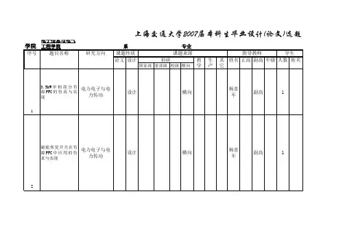
第十一届“恩智浦”杯全国大学生智能汽车竞赛技术报告学校:上海交通大学队伍名称:思源致远参赛队员:张兆瑞郭恒于欣禾带队教师:王冰王春香目录目录 (V)第一章引言 (2)1.1摘要 (2)1.2章节安排 (2)第二章整体方案设计 (3)2.1车体结构 (3)2.2硬件电路 (3)2.3控制算法 (3)第三章机械结构 (4)3.1车模重心调节 (4)3.2编码器安装 (4)第四章电路设计 (5)4.1总述 (5)4.2电源模块 (5)4.3主控模块 (6)4.4驱动模块 (6)4.5PCB图绘制 (7)第五章算法设计 (8)5.1概述 (8)5.2赛道识别算法 (8)5.3速度控制算法 (8)第六章总结 (10)第七章主要技术参数 (11)第一章引言1.1摘要全国大学生智能汽车竞赛至今已举办十届,通过十年间全国各地参赛队员的不断探索,较为传统的光电组已经形成了一套较为完整的体系,各类识别及控制算法均已较为成熟。
本设计为“恩智浦”杯第十一届全国大学生智能汽车竞赛的循迹行驶的方案,赛题组别为光电组。
本文主要介绍了从方案设计到硬件制作最后控制算法实现的过程,整个系统涉及硬件电路设计、控制方案、整车机械架构等多个方面。
最后通过长期的算法改进及参数调试测试了方案的可行性,并提升了控制算法的鲁棒性及整套系统的稳定性。
1.2章节安排在本文中,将详细介绍机械设计、硬件电路及软件设计的调试与实现过程。
其中机械设计包括重心调节以及各部分的安装等影响,硬件电路则包括各个子模块的功能、设计与实现。
而算法部分则系统的讲述了车模信息的采集、路径处理算法、舵机和电机控制策略等。
其中,第一章是讲述了智能车竞赛的背景和本文章节安排;第二章讲述了车模的整体设计;第三章分析硬件结构对于小车的影响;第四章是从各模块出发,详细讲述了硬件电路各部分功能;第五章讲述了车模的软件算法设计从基础训先控制和速度算法控制两个方面;第六章项目总结;第七章是车模的主要技术参数。
2010 International Conference on Intelligent Computation Technology and Automation Design and Implement of Responder Based on Freescale HCS12 Single ChipMicrocomputerCheng Qiming, Cheng Yinman, Wang Mingmei, Chang LinCollege of Electric Power and AutomationShanghai University of Electric PowerChangyang 2588 road, Yandpu district, Shanghai 200090, ChinaE-mail :Abstract—An 8-channel responder based on Freescale HCS12single chip microcomputer is designed. The responder candisplay the number of the first player correctly. It also can countthe scores and show the player with the highest score. Thesystem includes four modules: CPU12, the SCI serialcommunication, digital display tube and timer. Whencompetition signal input, it is been caught and then causeinterruption, the timer is used to time accurately, the serial portis used to send and receive the start answer signal, judgmentsignal and other signals, the digital display tube is used to showthe scores of the current player . LCD display tube showssubjects and answers. So the basic functions of the responder areachieved.Keywords--responder; single chip microcomputer; timer; inputcapture; interruptionI.I NTRODUCTIONResponder is also known as the first signal discriminator,which is widely used in various competitions. It can judge thenumber of the first player accurately, fairly and intuitively.Currently, a variety of quiz responder has emerged on themarket, in which a small responder is commonly designed withsmall-scale digital integrated circuit. Although the technologyhas been quite mature, but it is simple function, lowintelligence, high fault, simple display, less flexibility, notconvenience for upgrade, it has been unable to meet all kindsof requirements for intellectual competitions and varietyshows. Therefore, it is necessary to develop some kinds ofresponder which are more suitable for applications.In recent years, with the rapid development of science andtechnology, the applications of single-chip microcomputer arebecoming widely, which promotes the development oftraditional measurement and control technology. In this paper,Freescale HCS12 [1-3] is designed as a core component toachieve an intelligent digital responder with 8-channel [4-8], ithas some breakthroughs on technology, function and otheraspects, comparing with the past responder. It is characterizedby simple structure, powerful, good reliability, practicability,so that the competition can really carried out on just, fair andopen rules.II.F UNCTION OF RESPONDERThe basic functions of responder designed in this paper are:(1)The system can limit the competition time and answertime of the alarm;1 This work is supported by Leading Academic Discipline Project ofShanghai Municipal Education Commission (Project Number: J510301,J510303)978-0-7695-4077-1/10 $26.00 © 2010 IEEE DOI 10.1109/ICICTA.2010.128 1127(2)The system can identify the answer signal and identifythe player’s number;(3)The system can calculate score for each player anddisplay the scores.Responder can accommodate 8 players numbered 1 to 8. In addition, LED digital tubes are designed to display the latched data. After race host clears the system, if participants press switch, and after answer is certificated whether it is correct or not, the number of first player to answer in action is immediately shown by digital tubes. Responder should have a strong ability to distinguish players to answer in the action, its resolution reaches at least a few ms.III.I DEAS OF RESPONDER DESIGNAfter the requirements and functions of responder are analyzed, the following circuits are required in general:A Responder circuitThe circuit has two functions: one is to identify the number of the player who press button, and to save the number; the other is to prohibit the other players from buttoning or to make other buttons not available.B Timing circuitsHost can set competition time and answer time by the time pre-set-circuit. If nobody can answer question within the set time, all players will not get score, then the host will announce the answer. Besides, if someone gets the chance to answer the question, but does not give the right result before the allowable time, he or she won’t get the score, the overtime signal will be also send, the host will declare the right answer. Freescale HCS12 contains timer module, the timer module can be directly used.C Overtime circuitHCS12 will send overtime signal when time goes beyond the set time, this signal will be transferred to the PC computer by the serial port. The next question will be proceeded to answer.D Scores count and display circuit.When host presses the answer key, it is time to start to answer, if one player presses the answer key, his or her number will be recorded, his or her score will be counted and displayed on the LED digital tubes.Bedside the circuits designed above, some necessary logic designs are also necessary. The logic designs are as following:First, the host will read the question which will show in the LCD; next, the PC computer will send letter “k”, which means that play is beginning to competition. At the same time, timing circuit starts to work, if nobody gets the chance to answer the question within permitted time, microcontroller will send the word “chao shi”to PC computer; If someone presses the competition key within the specified time, microcontroller will send his or her number. If the time goes beyond the permitted time, PC computer will send “next”which means turning to the next question, the next question will be automatically showed to answer. If some player gets the chance to answer the question, his or her number and scores will decrease 1 automatically and show in the digital tubes, then microcontroller sends “next” to go on the next question. If the score is few than 0 after decreasing, player is eliminated. The right answer will show on the LCD. Finally, if all the questions are done, microcontroller will send “e”to end the game, then the scores of all players will be computed, the highest one will be shown on the digital tubes.IV.D ESIGN OF RESPONDER HARDWARE Responder hardware is firstly designed; Responder hardware is taken directly from the hardware resources of Freescale HCS12 development board developed by Suzhou University. The development board takes MC9S12DG128 as the core, using modular design approach, it extracts part of I/O resources, and it also provides each module with a corresponding interface circuit. It also provides A/D input channels, PWM low-pass filter circuits, 16-key keyboard input channels, 8-bit digital I/O circuits, SPI I/O circuits, SCI communication circuits, I2C bus I/O expansion circuits and so on.In this paper, the hardware modules, the pin connections and the corresponding interfaces of the development board are listed and unified to redesign by actual needs of the system. Figure 1 shows the hardware structure diagram of the selected part of development board.Figure 1. Diagram of hardware structureA Selection of hardware modulesThe responder designed in this paper is relatively simple, the I/O ports and the modules involved are not many.(1)The system uses push-button switch as the competition key, which is generally used as a switch input, there are 0 and 1. Here, the system need know whether the button is switched by somebody, the system need not care about the switch on or off.(2)Timer module is indispensable in timing circuit. Here, the timer module's functions are to limit time, and to capture input signals. This will be followed some of the circuit design described in detail.(3)LED digital tubes are used to show the participant’s number and scores in the display circuit. The system records the player's number and the corresponding score, and then transmits to the LED digital tubes through I/O ports. LCD is achieved by external connection module; it is used to display questions and answers.(4)LED small light is used to show whether somebody presses the competition button. If player answer, the small light will be bright, otherwise, it will not light.(5)SCI module is necessary in serial communication port. Since the signal that starts to answer needs to be send by PC computer, if there is no serial communication port, the whole system will be paralyzed. The function of SCI module is that receives the signal to HCS12, and then sends the player’s number to PC.B Design of hardware circuits1) Competition circuit designCompetition circuit captures competition signals by means of input capturing; there will be a interruption once the push- button switch jumps. 8 push-button switches are connected with 8 channels, so the system can know which player competes to answer the question by reading corresponding channel. In this paper, the 8 channels connect with input capture channels PT0~ PT7 of HCS12.2)Timing circuitAs the HCS12 has its own timing module, timing circuit don’t need to be designed, and internal timing module of HCS12 can be directly used.3)Overtime reminding circuitSmall light or buzzer could connect with any I/O port, but the system should ensure the selected I/O ports have not conflict with the I/O ports occupied by the module. Once the specified time is over, I / O port send a high level, and the LED small light is on. In this paper, the first pin of PA port is chosen as the alarm signal port; this pin is connected to the testing of small light.4)Electronic counter and display circuitThe scoring scores can be resolved by programming, but the displaying scores needs hardware connection, LED digital tubes and LCD are connected with corresponding I/O ports of HCS12, external LCD module should have the function of displaying Chinese characters.5)Communication connectThe development board has a 9-pin cable of RS232 serial port; it can be connected with PC computer by the cable.V.D ESIGN OF RESPONDER SOFTWAREA Design of software subprogram1)SCI subprogram(1)SCI initialization functionSCI initialization is to set corresponding register, mainly to set serial port baud rate, here baud rate is set to 9600 bps, the baud rate is:B t = f BUS / (16 * B R) (1) where, B R is set by SCI baud rate register, and it is a 16-bit register, is assigned twice, first set the low 8 bits, and then setthe higher 5 bits, the first three of high 8 bits are meaningless;f BUS is the bus frequency.The next is to set control registers (SCICR1 and SCICR2), here SCI serial port be allowed to run, and the normal code, 8- bit, no parity data is output. The D6 bit of the SCICR1 (SCISWAI) is a SCI allowing bit, SCI module is prohibited at SCISWAI=1, SCI module is allowed when SCISWAI=0; D4 bit (M bit) is a choice bit of pattern/character length, it is used to define the sending/receiving data format, 9-bit data transfer is allowed at M=1, 8-bit data transfer is allowed at M= 0; D1 bit (PE) is the parity enabling bit, PE=1 allows parity, PE = 0 does not allow parity. SCICR2 needs also to be set in order to receive and send data, the D3 bit of SCICR2 (TE) is a transmitter allowing bit, TE=1 allows to send, TE=0 prohibits to send; D2 bit is receiver allowing bit, RE=1 allows to receive, RE=0 prohibits to receive.(2)SCI sending functionFirstly, 1 bit sending function of serial port should be programmed. At the beginning, SCI status register 1 (SCISR1) needs to be judged, its D7 bit (TDRE) sends the empty flag of data register at TDRE=1, which means that the data to send has already moved into the sending shift register, if the data register is empty, the new data that is written into the data register can be sent. More bits data sending function calls repeatedly 1 bit sending functions until the sending is over.(3)SCI receiving functionSimilarly, 1 bit receiving function of serial port is programmed. Here, SCI status register 1 (SCISR1) is judged, its D5 bit (RDRF) represents the full flag of the receiving data register. RDRF=1 means that the receiver is full, the received data can be read from the SCI data register, then, the data needs to be read out from data register (SCIDR). The receiving data is one more step than the sending data, which it is to determine whether any data has been received. If the receiving process is failed, FFH data will be returned. More bits data receiving function call repeatedly 1 bit receiving function, and the system will report the receiving error as long as there is 1 bit receiving failure.2)Timer subprogram(1)Timer initializationWhen timer is initialized, timer is prohibited to work until timer is used. The D7 bit (TEN) of timer control register 1(TSCR1) is an enabling bit of timer, timer is enabled at TEN=1, and timer is disabled at TEN=0. The following step is to allow the timer interrupt and to prohibit the timer reset. The D7 bit (TOI) and the D3 bit (TCRE) of timer control register 2 (TSCR2) are respectively the enabling bit of timer overflow interrupt and the reset enabling bit of timer counter, timer interrupt is allowed at TOI=1, otherwise, timer interrupt is not allowed at TOI=0. When OC7 is successfully compared, the counter can be reset at TCRE=1, it can’t be reset at TCRE=0; D2 ~ D0 bits (PR2 ~ PR0) of TSCR2 are the selection bits of frequency factor, they are used to set the division factor of bus clock frequency, frequency division factor p can be 1,2,4,8,16, 32, 64 or 128. The overflow time of timer can be described as following:t=np/f BUS (2) where, n is the count value of counter; f BUS is the bus clock frequency; p is the frequency division factor. In this paper, n = 216 = 65536, p is chosen to be 2, t≈0.03s, t is much closed to 1/38s, 38 interruptions is about 1s.(2)Input capturing initializationFirst, the option is to capture input or to compare output. The select register of input capturing/output comparing (TIOS) is used to do this work, the Dx bit (IOSx) of the register is the select bit of x channel, the x channel is set as the output comparing channel at IOSx = 1, and it is set as the input capturing channel at IOSx = 0. In our design, because 8 players take pert in the competition, 8 channels should all be set as input capturing channels, namely TIOS = 0x00.After input capturing is set, the interruption also needs to be open, which it should be done after the competition is allowed.3)Subprogram of LED digital tubes(1)Initialization of LED digital tubesLED digital tubes are used to dynamic display, its initialization is the I/O port initialization, the direction registers of corresponding I/O ports (the pins of 8-bit data port are connected with 7-segment digits and decimal point of digital tubes; the pins of 4-bit bit choice are connected with 4 digital tubes) are set to be output, that is, data port is 0xFF, bit choice port is 0xF0.(2)Display of LED digital tubesThe basic idea of LED digital tubes display is that the display codes of all the numbers and the chip select code of the displaying bits are stored into the corresponding registers, when display functions are called, the parameter numbers of functions can match with the numbers and the bits in the tables of number display code and chip select code4)LCD display(1)LCD initializationThe module is enabled and the lattice size is defined as 8*8 or 8*10, the display format is defined as 1 row or 2 rows, the display of Chinese characters is used.(2)Subprogram of LCD displayThe emphasis of the program is the display of Chinese characters. Chinese characters are identified by two ASCII codes. The ASCII codes of Chinese characters to be displayed are recorded into data registers.B Design of interrupt service subprogram1)Subprogram of overflow interruptionThe frequency division factor has been set in the program of timer initialization, 38 interruptions is about 1s, so the counter variable needs to be set, it adds 1 automatically after each interruption, it calls the second accumulating function after 38 interruptions. It needs to be noted that the interruption flag register 2 (TFLG2) is set to 0 after each overflow interruption. Otherwise, the system is always identified as overflow interrupt. D7 bit of the register is TOF bit, when the 16-bit running counter changes from $FFFF to $0000, the overflow interrupt occurs, this bit is set to 1, this bit can be cleared by writing 0 to it, other 7 bits are invalid. The flow of overflow interrupt is shown in Figure 2.2)Subprogram of input capturing interruptionThe main task of input capturing interruption program is to judge whether player competes to answer and to record the player’s number. The interrupt flag bit needs to be set, it is set to 1 when an interrupt happens, which means that someonecompetes to answer, and then the person number will be read.Interrupt flag register 1 (TFLG1) of main timer is used to readthe interrupt channel. Its Dx bit (CxF) is the interrupt flag ofinput capturing / output comparing channel x, when an inputcapturing / output comparing event happen, the correspondingbit is set to 1, the channel number of correspondinginterrupting can read from TFLG1 register and it is also thenumber of competition player. To note that, the flag registerneeds to be cleared after the flag register is read. The flagregister can be cleared when the appropriate channel is set to 1.The flow of input capturing interrupt is shown in Figure 3.VI.C ONCLUSIONSResponder is one of the essential devices in variousknowledge and intellectual contests, the development of betterand more intelligent digital responder is very significant.Responder designed in this paper can achieve a responder'sbasic functions through experimental prototype testing.It reaches the design target with reasonable design, simplestructure, good commonality, strong function, reliable answerand quick reaction. However, as hardware limitations ofdevelopment board, some functions have not been able toachieve, such as the development board does not have enoughLED digital tubes to display all player’s scores simultaneously,the host can not adjust answer time according the difficulty ofthe question and so on. These issues will remain to beaddressed in future development.Figure 2. Flow of overflow Figure 3. Flow of input capturinginterrupt interruptC The main program designBefore the start of the main program, the total interruptionsare turned off and each module is initialized. The initializationof each module has been done in the correspondinginitialization subprogram of each module. Here we only needcall the corresponding initialization subprogram. After theinitialization of each module is completed, the totalinterruptions should be turned on. The main body of the mainprogram is a loop structure; there are also several sub-cycles inthe main loop, which are used for the cycle waiting of eachloop. The flow of the main program is shown in Figure 4.After the completion of the initialization, the system has beenwaited for the signal of competition start with the circularmode until the signal comes. When this signal is received, thesystem checks whether the cycle time is overtime, if it isovertime, the system changes to the next question, otherwise,the system checks the competition signal, if some playercompetes to answer, then the system checks whether theanswer time is out, if the time is not out, the system judgeswhether the result is true, if the result is right, the player isadded 1 point, otherwise, the player is subtracted 1 point, andthe system enters the next question. To the player whose scorewill be subtracted, the system needs to check whether the scoreis low than 0, if it does, this player’s input channel is turnedoff. To be noted that, if the competition flag is 1, it should becleared.Figure 4. Flow of the main programR EFERENCES[1] Steven F B, Daniel J P. Embedded systems–using the HCS12microcontroller design and application [M]. NewYork: PublishingHouse of Electronics Industry, America, 2006.[2] Wang Yihuai, Liu Xiao. Embedded systems–the design and applicationof HCS12 micro controller [M]. Beijing: Beijing University ofAeronautics and Astronautics Press, 2008.[3] Wang Wei. Principle and applications of HCS12 microcontrollers [M].Beijing: Beijing University of Aeronautics and Astronautics Press,2007.[4] Zhang Ruixi. Design of quiz responder [J]. Mechanical and ElectricalEngineering and Technology, 2007, vol.36, no.8, pp.51-52.[5] Li Ming, Tan Andrew, Zhu Shunli. 8-way intelligent responder basedon the LPC932 single chip microcontroller [J]. Ordnance Automation,2007, vol.26, no.7, pp.70-71.[6] Chou Kungming, Zhou Chenchen. Design of 9-way multi-functionalquiz responder based on the single chip microcontroller AT89C2051 [J].Modern electronic technology, 2006, vol.25, no.20, pp.4-6.[7] Wang Gongtang, Yang Shanying. 16-way responder based on thePIC16F873 [J]. Computer Development & Applications, 2006, vol.19 ,no.9, pp.9-13.[8] Gong Changlay. Design of intelligent responder controlled by singlechip microcomputer [J]. Guangdong Automation and InformationEngineering, 2003, no.3, pp.28-30.基于飞思卡尔HCS12单片机设计和实施的抢答器程启明,程尹曼,汪明媚,常林上海电力学院电力与自动化工程学院,上海,200090摘要——基于飞思卡尔HCS12单片机的八通道抢答器设计。
上海交通大学继续教育学院《微机原理与应用》学位课程大纲一、基本信息1、教材名称:推荐教材:李继灿主编,新编16/32位微型计算机原理及应用(第5版),清华大学出版社,2013年参考教材:1、周明德编著,微型计算机系统原理及应用(第5版),清华大学出版社,2008年2、戴梅萼编著,微型计算机技术及应用(第4版),清华大学出版社,2008年2、考试题型及分值:单项选择题10分,填空题20分,判断题10分,简答题20分,程序题20分,综合运用题20分3、考试形式:闭卷4、考试时间:2小时二、课程内容情况(一)课程内容简介本课程是计算机专业的核心课程之一,是一门面向应用的、具有很强的实践性与综合性的课程,主要任务是使学生掌握微机硬件体系结构的基本知识,在微机汇编语言程序设计和硬件接口技术编程方面掌握基本内容和应用技巧,并达到相应的实际应用开发水平。
本课程提供微机原理与应用的基本理论与技术,比较有深度,具有理论性强、概念抽象、技术更新快等特点。
包括教学课和实践操作课两部分。
教学课以课堂讲解形式使学生了解微型计算机的基本结构及其工作原理,掌握指令系统及汇编语言程序设计方法、微型计算机与外设的数据传输方式、中断技术、可编程定时器/计数器、串并行接口技术,以及微机最新发展趋势等。
实践操作课以上机形式使学生熟悉汇编语言的编程环境与特点,能编写、调试、运行完成一定功能的汇编语言源程序。
本课程教学目的在于使学生全面掌握微机的基本工作原理和程序设计方法。
注重理论联系实际,加强实践环节,培养学生分析问题和解决问题的能力,使学生具有微型计算机应用系统分析能力和初步设计能力。
(二)重点内容简介(1)微机系统导论(约5%)考核内容:–微机系统组成–微机硬件系统结构–微处理器的性能指标–微机总线结构考核要求:理解:微机工作过程CPU对存储器的读/写操作及其区别了解:存储器组成程序计数器与累加器功能微机系统的主要性能指标当前PC机的标准配置掌握:微机的软、硬件系统组成微处理器、微型计算机、微型计算机系统的概念微机硬件系统组成框图及各部分的主要功能微处理器组成指令和程序的概念重点掌握:微机系统的组成微处理器性能指标(字长、内存容量、主频、运算速度、存取周期)微机总线结构计算机常用术语(位、字节、字) 的含义(2)微机运算基础(约5%)考核内容:–各种进位计数制之间的相互转换–原码、反码、补码的表示范围–原码、反码、补码、真值之间的相互转换–二进制数的加减运算与逻辑运算–进位和溢出的区别考核要求:理解:进位计数制的基本特点二进制数的乘、除算术运算了解:ASCII编码掌握:补码运算重点掌握:二、十、十六进制的相互转换无符号数、带符号数、真值、机器数的区别二进制数的加、减算术运算二进制数的与、或、非、异或逻辑运算进位和溢出的概念(3)8086微处理器及其系统(约15%)考核内容:–8086微处理器特点–通用寄存器组,段寄存器,标志寄存器–时序、指令周期、总线周期、时钟周期、分时复用总线、物理地址,逻辑地址,偏移地址–总线接口单元与执行单元组成与功能–20位物理地址形成–指令队列与堆栈–规则字与非规则字–最小工作方式与最大工作方式特点考核要求:理解:8086主要引脚的功能了解:微处理器发展过程8086引脚功能8086存储器组织掌握:最小工作方式与最大工作方式区别8086微处理器特点重点掌握:指令周期、总线周期、时钟周期的概念存储器的分段设计思想逻辑地址与物理地址的关系8086 CPU的内部结构8086的寄存器结构指令队列与堆栈的特点与操作(4)8086指令系统(约10%)考核内容:–8086的寻址方式–通用数据传送指令:MOV,PUSH,POP–目标地址传送指令:LEA–I/O数据传送指令:IN,OUT–加法指令:ADD,ADC,INC–减法指令:SUB,SBB,DEC,CMP–逻辑运算指令:AND,OR,XOR,TEST–移位指令:逻辑移位(SHL,SHR)算术移位(SAL,SAR)–循环控制类指令:无条件转移指令:JMP条件转移指令:无符号(JA,JAE,JB,JBE)有符号(JG,JGE,JL,JLE)单标志:JE/JNE循环控制指令:LOOP,JCXZ考核要求:理解:8086指令系统特点段内转移与段间转移,短转移无条件转移和条件转移区别循环移位指令了解:8086指令格式处理器控制类指令功能中断指令执行过程掌握:6大类指令系统基本用法重点掌握:8086的寻址方式数据传送类指令算术运算(加、减)类指令逻辑运算类指令移位类指令循环控制指令(条件转移、无条件转移、循环控制)(5)8086汇编语言程序设计(约15%)考核内容:–读、写汇编语言程序–程序框图绘制方法–机器语言、汇编语言以及高级语言特点–常用汇编伪指令的含义和用法考核要求:理解:源程序结构顺序程序、分支程序、循环程序的基本设计方法了解:汇编语言的特点、汇编语言的基本语法掌握:常用汇编伪指令的含义和用法:符号定义伪指令、数据定义伪指令、段定义伪指令汇编语言程序的格式和运行方法重点掌握:读写、运行、调试汇编语言程序指令语句与伪指令语句的异同点变量与标号的区别(6)半导体存储器(约10%)考核内容:–半导体存储器分类及特点–静态RAM、动态RAM组成及特点–地址译码方式–存储器与CPU的连接–位扩充与地址扩充技术考核要求:理解:RAM和ROM的工作特点微处理器与存储器的连接方法8086的存储器组织了解:DRAM的刷新原理新型存储器技术发展动向与趋势掌握:半导体存储器的性能指标重点掌握:半导体存储器分类、组成与功能静态RAM、动态RAM组成和特点存储器的分段方法存储器芯片的扩充技术(7)输入与输出接口技术(约10%)考核内容:–接口的概念与功能–接口电路的信息种类–程序传送方式特点及程序流程:无条件传送,程序查询传送–中断传送方式特点–直接存储器存取传送特点考核要求:理解:CPU与外设之间的连接了解:I/O接口及其功能接口电路的基本结构掌握:中断的分类输入、输出的信息种类重点掌握:CPU与外设数据传送方式与控制方式(8)中断技术(约15%)考核内容:–中断源,中断向量,中断向量表,中断类型码,中断优先权–断点与现场–中断分类–中断类型码与中断向量关系–响应中断的条件–中断响应及处理过程–8259A内部8个部件功能及其关系考核要求:理解:8086中断系统了解:可编程中断控制器8259A引脚及其功能掌握:中断的有关概念8259A内部结构框图重点掌握:中断分类CPU响应中断及处理过程(9)可编程接口芯片及应用(约15%)考核内容:–接口分类与功能–8253-5内部结构–8255A 3个端口的特点与差异性–8255A 3种工作方式–8253-5和8255A 应用考核要求:理解:接口基本结构的特点掌握:定时/计数器8253-5的主要性能、工作方式和初始化编程方法并行接口8255A的主要性能、工作方式和初始化编程方法重点掌握:8253-5内部结构特点8255A 3个端口的特点与差异性接口分类与功能8253-5和8255A 应用。


微机第一次作业1、11000110为二进制补码,该数的真值为(B )。
a. +58b. -58c. -198d. +1982、16个字数据存储区的首址为70A0H:DDF6H,末字单元的物理地址为( C )。
a. 7E816Hb. 7E7F8Hc. 7E814Hd. 7E7F6H3、8位二进制数的原码表示范围为( A )。
a. -127 ~+127b. 0 ~255c. -128 ~+128d. -128 ~+1274、完整的计算机系统应包括(B )。
a. 运算器、控制器、存储器b. 硬件设备和软件系统c. 主机和外部设备d. 主机和应用程序5、存储字长是指(B )。
a. 以上都是b. 存储单元中二进制代码个数c. 存储单元的个数d. 存储单元中二进制代码组合6、运算器执行两个补码表示的整数加法时,产生溢出的正确叙述为(C )。
a. 相加结果的符号位为1则产生溢出b. 最高位有进位则产生溢出c. 相加结果的符号位与两同号加数的符号位相反则产生溢出d. 相加结果的符号位为0则产生溢出7、堆栈存储器存取数据的方式是(A )。
a. 先进后出b. 都可以c. 随机存取d. 先进先出8、下列数中最小的数是(D )。
a. (97)10b. (62)16c. (142)8d. (1011011)29、程序计数器PC的作用是(B )。
a. 保存CPU要访问的内存单元地址b. 保存将要执行的下一条指令的地址c. 保存正在执行的一条指令d. 保存运算器运算结果内容10、若某CPU具有64GB的寻址能力,则该CPU的地址总线宽度为(A )。
a. 36b. 64c. 32d. 2411、8086系统中,每个逻辑段的最多存储单元数为(D)。
a. 1MBb. 256Bc. 根据需要而定d. 64KB12、在机器数(C )中,零的表示形式是惟一的。
a. 原码b. 反码c. 补码d. 原码和反码13、指令队列具有(B )的作用。
满分100分,题型:30题选择×2=60分,3题大题40分(印象中好像是10+8+22)。
题目都是基础题,下面回忆几题吧(有些实在想不起来了)。
====================================一、选择题(选项就省了,题目顺序不对,只是大概的回忆)1、x86系统的中断向量的地址范围是?2、要表示3位十进制数至少需要几位二进制数?3、USB接口共有几条线?4、关于内存的刷新频率的问题5、关于总线带宽的问题6、两个数相减,标志寄存器位OF、CF、ZF的变化7、存储器的地址问题8、………………………………30、…………30题太多了实在回忆不起来了,Sorry!总之,题目都是非常非常基础的,我感觉没有什么难的,15分钟30题就搞定了。
二、解答题1、给了一幅存储器的连接图,要求写出2片存储器的地址范围和容量(A0和ALE参与奇偶地址的片选)2、关于码制转换的,已知[-1/2X]原,要求写出[-2X]原,[-2X]反,[-2X]补3、关于接口电路的问题给了一幅图,有138,8253,8255,8259,8251等,1)已知8253的口地址范围,要求画出138和8086地址总线的连接图;2)已知8259 IRQ0的中断向量地址,要求写出IRQ3、IRQ7的中断向量地址3)根据图写出8255的口地址范围(A口、B口、C口和控制口)4)要求通过8253产生周期性中断请求信号,确定8253工作方式,并求出计数初值5)已知8251传送的字符格式,要求8251的波特率====================================腹有诗书气自华腹有诗书气自华《微型计算机原理与应用》参考书目:《微型计算机原理与接口技术》(第三版)吴秀清、周荷琴编中国科技大学出版社 2005 ; 《微机原理与接口技术》王玉良等编北京邮电大学出版社 2000复习大纲:第一章 绪论计算机的发展概况与趋势;计算机的运算基础;计算机系统的组成原理。