EMI调试实践应用指南
- 格式:pdf
- 大小:1.38 MB
- 文档页数:12
频谱分析仪EMI 使用手册本文档适用于以下机型:UTS5000A系列UTS3000B/T系列UTS3000A系列UTS1000B/T系列UTS1015E系列REV12023.12.18序言尊敬的用户:您好!感谢您选购全新的优利德仪器,为了正确使用本仪器,请您在本仪器使用之前仔细阅读本使用手册全文,特别有关“安全注意事项”的部分。
如果您已经阅读完本使用手册全文,建议您将此使用手册进行妥善的保管,与仪器一同放置或者放在您随时可以查阅的地方,以便在将来的使用过程中进行查阅。
版权信息UNI-T优利德科技(中国)股份有限公司版权所有。
UNI-T产品受中国或其他国家专利权的保护,包括已取得或正在申请的专利。
本公司保留更改产品规格和价格的权利。
UNI-T保留所有权利。
许可软件产品由UNI-T及其子公司或提供商所有,受国家版权法及国际条约规定的保护。
本文中的信息将取代所有以前出版的资料中的信息。
UNI-T是优利德科技(中国)股份有限公司[UNI-TREND TECHNOLOGY(CHINA)CO.,LTD]的注册商标。
如果在适用的保修期内证明产品有缺陷,UNI-T可自行决定是修复有缺陷的产品且不收部件和人工费用,或用同等产品(由UNI-T决定)更换有缺陷的产品。
UNI-T作保修用途的部件、模块和更换产品可能是全新的,或者经修理具有相当于新产品的性能。
所有更换的部件、模块和产品将成为UNI-T的财产。
以下提到的“客户”是指据声明本保证所规定权利的个人或实体。
为获得本保证承诺的服务,“客户”必须在适用的保修期内向UNI-T通报缺陷,并为服务的履行做适当安排。
客户应负责将有缺陷的产品装箱并运送到UNI-T指定的维修中心,同时预付运费并提供原购买者的购买证明副本。
如果产品要运送到UNI-T维修中心所在国范围内的地点,UNI-T应支付向客户送返产品的费用。
如果产品送返到任何其他地点,客户应负责支付所有的运费、关税、税金及任何其他费用。
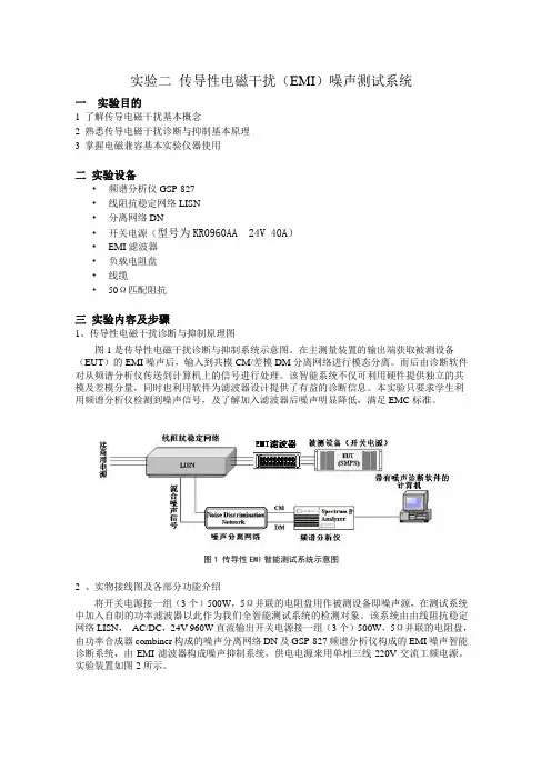
实验二传导性电磁干扰(EMI)噪声测试系统一实验目的1 了解传导电磁干扰基本概念2 熟悉传导电磁干扰诊断与抑制基本原理3 掌握电磁兼容基本实验仪器使用二实验设备•频谱分析仪GSP-827•线阻抗稳定网络LISN•分离网络DN•开关电源(型号为KR0960AA 24V 40A)•EMI滤波器•负载电阻盘•线缆•50Ω匹配阻抗三实验内容及步骤1、传导性电磁干扰诊断与抑制原理图图1是传导性电磁干扰诊断与抑制系统示意图。
在主测量装置的输出端获取被测设备(EUT)的EMI噪声后,输入到共模CM/差模DM分离网络进行模态分离。
而后由诊断软件对从频谱分析仪传送到计算机上的信号进行处理。
该智能系统不仅可利用硬件提供独立的共模及差模分量,同时也利用软件为滤波器设计提供了有益的诊断信息。
本实验只要求学生利用频谱分析仪检测到噪声信号,及了解加入滤波器后噪声明显降低,满足EMC标准。
图1 传导性EMI智能测试系统示意图2 、实物接线图及各部分功能介绍将开关电源接一组(3个)500W,5Ω并联的电阻盘用作被测设备即噪声源,在测试系统中加入自制的功率滤波器以此作为我们全智能测试系统的检测对象。
该系统由由线阻抗稳定网络LISN,AC/DC,24V 960W直流输出开关电源接一组(3个)500W,5Ω并联的电阻盘,由功率合成器combiner构成的噪声分离网络DN及GSP-827频谱分析仪构成的EMI噪声智能诊断系统,由EMI滤波器构成噪声抑制系统,供电电源来用单相三线220V交流工频电源。
实验装置如图2所示。
图2 以开关电源拖带阻性负载为被测设备的实验装置图⑴线阻抗稳定网络LISN:目前国际标准进行的传导性电磁干扰测量系采用线阻抗稳定网络LISN,,其核心是通过电感、电容和标准50 阻抗构成的测试网络(前一节已做介绍),作为获得被测设备EUT所产生的传导干扰信号的接受器。
⑵噪声分离网络DN:,LISN只能测量到传导性EMI噪声的混合信号而不能从中检测出CM 和DM分量,但EMI滤波器设计却分为共模和差模滤波器两种。
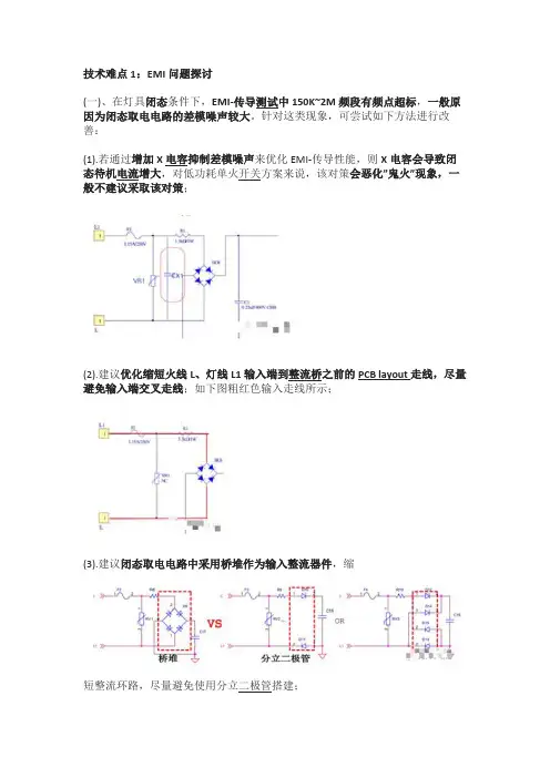
技术难点1:EMI问题探讨(一)、在灯具闭态条件下,EMI-传导测试中150K~2M频段有频点超标,一般原因为闭态取电电路的差模噪声较大。
针对这类现象,可尝试如下方法进行改善:(1).若通过增加X电容抑制差模噪声来优化EMI-传导性能,则X电容会导致闭态待机电流增大,对低功耗单火开关方案来说,该对策会恶化”鬼火”现象,一般不建议采取该对策;(2).建议优化缩短火线L、灯线L1输入端到整流桥之前的PCB layout走线,尽量避免输入端交叉走线;如下图粗红色输入走线所示;(3).建议闭态取电电路中采用桥堆作为输入整流器件,缩短整流环路,尽量避免使用分立二极管搭建;(4).闭态取电电路中输入大电容电路可预留LC或π型滤波电路作为EMI对策。
设计注意点:此对策器件选型、参数可能会对待机功耗有影响,调试过程中须留意待机电流的变化;(二)、在灯具开态条件下,开态取电电路选取合适的GATE驱动电阻。
此GATE为低频开关信号,驱动电阻R4建议选取20~30K,让MOSFET开启更缓。
若R4不够大或MOSFET的结电容偏小,EMI会比较差,可根据EMI情况调整。
下图为驱动电阻R4电路图示以及不同驱动电阻R4阻值传导测试对比结果:驱动电阻R4电路图示不同驱动电阻R4阻值传导测试对比技术难点2:支持大功率单火取电开关的探索随着智能家居产品的多元化、多样化,市面上出现带触摸屏、语音交互、音乐、网关等更多功能的智能开关产品,这类智能开关产品的功耗都在5V/0.5A 以上,且基本上都是采用零火线供电方案,传统单火取电方案不能满足需求。
为满足这类产品可直接应用在单火线布线场景中,需要开发一款可以支持大功率取电的单火开关。
这类产品应用在单火场景会碰到的技术难点:无论在灯具关态还是开态,其功耗都在5V/0.5A以上,这对单火取电技术提出了更高的要求。
在此列举其中一种支持大功率单火取电的解决思路,其电路框架示意图如下:在灯具两端并联设计一款分流电路,配合单火智能开关的取电电路输出不小于5V/0.5A功率给智能开关系统电路供电。
《EMI对症分析-EMI整改》第一篇:emi对症分析-emi整改1mhz以内----以差模干扰为主1.增大x电容量;2.添加差模电感;3.小功率电源可采用pi型滤波器处理(建议靠近变压器的电解电容可选用较大些)。
1mhz---5mhz---差模共模混合,采用输入端并联一系列x电容来滤除差摸干扰并分析出是哪种干扰超标并以解决,1.对于差模干扰超标可调整x电容量,添加差模电感器,调差模电感量;2.对于共模干扰超标可添加共模电感,选用合理的电感量来抑制;3.也可改变整流二极管特性来处理一对快速二极管如fr107一对普通整流二极管1n4007。
5m---以上以共摸干扰为主,采用抑制共摸的方法。
对于外壳接地的,在地线上用一个磁环串绕2-3圈会对10mhz 以上干扰有较大的衰减作用;可选择紧贴变压器的铁芯粘铜箔,铜箔闭环.处理后端输出整流管的吸收电路和初级大电路并联电容的大小。
对于20--30mhz,1.对于一类产品可以采用调整对地y2电容量或改变y2电容位置;2.调整一二次侧间的y1电容位置及参数值;3.在变压器外面包铜箔;变压器最里层加屏蔽层;调整变压器的各绕组的排布。
4.改变pcblayout;5.输出线前面接一个双线并绕的小共模电感;6.在输出整流管两端并联rc滤波器且调整合理的参数;7.在变压器与mosfet之间加beadcore;8.在变压器的输入电压脚加一个小电容。
9.可以用增大mos驱动电阻.30---50mhz普遍是mos管高速开通关断引起,1.可以用增大mos驱动电阻;2.rcd缓冲电路采用1n4007慢管;3.vcc供电电压用1n4007慢管来解决;4.或者输出线前端串接一个双线并绕的小共模电感;5.在mosfet的d-s脚并联一个小吸收电路;6.在变压器与mosfet之间加beadcore;7.在变压器的输入电压脚加一个小电容;8.pcb心layout时大电解电容,变压器,mos构成的电路环尽可能的小;9.变压器,输出二极管,输出平波电解电容构成的电路环尽可能的小。
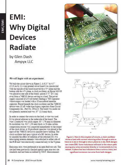
Figure 1: Here in the simplest of circuits, a clock oscillator drives a load with current returning either through a wire or trace as in (a) or through a return plane as in (b)� Both designs can create EMI� Some inductance will exist in the return path causing any wires connected directly or incrementally to it to radiate� A plane has less inductance than a wire or trace, butsignificant emissions can arise from both designs�EMI: Why Digital Devices RadiateFigure 2: We assembled and tested this circuit to see if theory would correctly predict observed emissions�wereytakenyatopyay.8ymeterywoodenyturntableywhichywasy rotatedytoydetectymaximumyemissions.yAsyexpected,ywheny theyattachedytelescopingyantennasywereytunedyforyresonance,y maximumyemissionsyatytheyresonantyfrequencyywereyobservedy whenytheytelescopingyarmsylayyparallelytoyayhorizontallyy polarizedyantenna.yMeasurementsywereyperformedyatyaydistanceyofy10ymetersyandytheyantennaywasyraisedyandyloweredy toydetectymaximumyemissionsyoveryay1ytoy4ymeteryrange.y Weybeganyourystudyybyyfocusingyonyoneyfrequency,ytheyfifthy harmonicyofytheyclockyaty125yMHz.yTheytelescopingyelementsy wereytunedytoyresonanceyatythatyfrequencyyandyleftythereyforythey durationyofytheytest.yTheycircuityshownyinyFigurey2yproducedy 39.4ydBuV/myofyradiationyaty10ymeters.yOurynextytaskywasytoyexplainywhyythisycircuityradiates,y calculateytheypredictedyradiationyandyseeyifyitymatchedyoury measuredyresults.yItyisynowywellyestablishedyoneymechanismycausingyradiationy atytheseyfrequenciesyisythatyillustratedyinyFigurey1.yAyclockyory clock/driverycombinationyservesyasyaysourceydrivingyaydistanty load.yTheysignalyproducedyisyaytrapezoidalywavey(squareywavey withyfiniteyriseyandyfallytimes)yandytheysourceyhasyanyinternaly resistance,yR o ,yandyinductance,yL o .yTheyloady(Z 2yinyFigurey1)y isyaylogicygate,ywhich,yforyMOSybasedytechnologies,ycanybey modeledyasyaycapacitance.yAyseriesyresistance,yR S yisysometimesy insertedyatytheysourceyendytoysuppressyringing.yTheoryystatesythatythey“drivenywire,”ythatyisytheywirey connectingytheysourceytoytheyloadycanybeycharacterizedyasy anyinductor.ySimilarly,ytheyreturnytracey(Figurey1a)yoryplaney (Figurey1b)ycanyalsoybeycharacterizedyasyanyinductoryatyy 125yMHzy(Z3).yAyreturnyplaneyhasyayconsiderablyylowery inductanceythanyayreturnytrace.yIfyweyknowytheycurrentypassingythroughytheyreturnyplaneyory trace,ythenybyyusingytheyinductanceyvariousymodelsypredicty weycanycalculateyayvoltageydropyacrossytheyreturnytraceyory plane.yThisyvoltageydropywillydriveyanyywiresyattachedytoythey returnypathyasyifytheyywereyantennas.yBasically,ytheyreturnytracey oryplaneyservesyasyaylowyimpedanceyvoltageysourceydrivingy attachedywires.yAnyywiresydirectlyyoryincrementallyyconnectedy toytheyreturnytracesyoryplaneywillyradiate.yInyayworst-caseyscenario,ytheywiresyattachedytoytheyreturnytraceyoryplaneycanybey stretchedyoutytoyformyaydipoleyresonantyatyoneyofytheyharmonicsy ofytheyclockyoscillator.yThatyisywhatywasydoneyhere.y AyTektronixyCT1ycurrentyprobeywasyusedytoymeasureythey currentythroughytheydrivenywire.yTheycurrentywaveformyisy shownyinyFigurey3.yTheyamplitudeyofytheycurrentywasyalsoy measuredybyyusingyayspectrumyanalyzer.yAtyayfrequencyyofyy 125yMHzytheyamplitudeyofytheycurrentymeasuredywasyy2.8ymilliampsyRMS.y(Theycurrentyprobeywasyremovedyduringy EMIytesting.)yEMI: Why Digital Devices RadiateTheyinductanceyofytheyreturnyplane,yaccordingytoyKadenyasyreportedybyyLeferinky[1],yis:yWhere:yL return plane y=yreturnyplaneyinductancey w y=ywidthyofytheyplaneyinymetersyd y=ydistanceybetweenytheydrivenytraceyandytheyreturnyplaneyiny metersyl y=ylengthyofytheydrivenytraceyinymeters,y l >>d yµ0y=ypermeabilityyofyfreeyspacey=y4πyxy10-7yHenries/meteryHockanson,yetyalymadeyayslightlyydifferentypredictiony[2].yItyis:Theyconstanty k yisygeometryydependent.yIty isyayfunctionyofytheycurrentydistributionyiny theyreturnyplane.yKaden’syformulayassumesy thatytheyreturnycurrentyspreadsyoutyevenlyy acrossytheyreturnyplane.yButythisyisynotyso.yIty isynowyknownythatytheycurrentyinytheyreturny planeyconcentratesybeneathytheydrivenytrace.y Theyconstanty k ythereforeycanybeydifficultytoy predict.yEstimatesyplacey k ybetweeny2yandy5.y We’llyuseytheyupperylimityofythisyrange,y k =5ytoyarriveyatyayworst-caseypredictionyfory theyradiation.yInsertingytheyvaluesyforythey circuityinyFigurey2y(d =.76ymm,y w =114ymm,y l =9.5ycm)yyieldsyanyinductanceyvalueyfory theyreturnyplaneyofy.033ynH/cmyory.32ynHyy inytotal.yAty125yMHzyanyimpedanceyofyy .25jyohmsywouldyresultydueytoythisyinductance.yTheyvoltageydropyacrossythey returnycanybeyreadilyycomputedyfromythey measuredycurrentyaty125yMHzyy(2.8ymilliamps).yTheyvoltageyacrossythey return,ytheymodelypredicts,yisy.07yV olts.y Thisyvoltageydrivesytheyattachedytelescopingy antenna,ytheyarmsyofywhichywereyadjustedy toyhalfywaveyresonanceycreatingyayhalfywaveyresonantydipole.yWeycanycalculateythey predictedyfreeyspaceyemissionsyfromyayhalfy waveyresonantydipoleyusingytheyfollowingyformulay[3]:yFigure 3: The current in the driven wire, and therefore the return, was measuredusing a Tektronix CT1 current probe�Figure 4: Slicing the return raises the return inductance resulting in increasedradiation�EMI: Why Digital Devices RadiateWhere:yE(V/m)y=yfreeyspaceyfieldystrengthyG ant y=ygainyofyayresonantyhalfywaveydipoleyoveryisotropicy=y 2.1ydBiy=y1.3yr y=ydistanceyfromytheycircuitytoytheymeasuringyantennayiny metersy=y10ymetersyV r y=ytheyvoltageydroppedyacrossytheyreturnyplaney=y.07yV oltsy Z ant y=yimpedanceyofytheyradiatingyantennay=y73yohmsyforyay halfywaveydipole.yOurymodelypredictsyfreeyspaceyradiationyofy35.2ydBuV/myatyy 10ymeters.yTestingyoveryaygroundyplaneyaffectsytheyimpedanceyofy theyradiatingyantennaysomewhatyandyprovidesyforygroundy reflection.yAsyanyapproximation,yweycanyassumeythatytheynety ofytheseyeffectsyisytoyincreaseyemissionsybyy5ydByaty125yMHz.y Usingythisyadjustment,yourymodelypredictsyemissionsyofyy 40.2ydBuV/m,yquiteycloseytoytheymeasuredyvalue.yOurysimpleycircuityofyFigurey2yusedysolidypoweryplanes.y Practicalypoweryplanes,yhowever,yareynotysolidybutyarey interruptedybyyholesyandygaps.yModelsyproposedybyyresearchersypredictythatyemissionsywillyriseydramaticallyyifythey returnyplaneyisyinterruptedywithyayslityasyshownyinyyFigurey4.yTheyslitycutsycompletelyythroughytheyPCB,yinterruptingybothytheyV+yandyV-yplanes.yItyisy.065”y(1.65ymm)y wideyandyextendsyfromyoneyedgeyofytheyboardytoyaypointy1”y (2.54ycm)ypastytheytrace.yTheymeasuredyemissionsyaty125yMHzy didyriseydramatically,ytoy59.8ydBuV/m.Hill,yetyal.,y[4]ymodelsytheyincreasedyinductanceybyyanalyzingy theygapyasyayshortedytransmissionyline.yDash,yetyaly[5]ycalculatesythisyinductanceytoybe:yWhere:yw y=ytheywidthyofytheyplaneytoytheyleftyandyrightyofytheyslotyiny metersys y=ytheywidthyofytheyslotyitselfyinymetersy w y>>y s yandy L gap y<<yλyApplyingythisyformulaytoyourytestycircuity(s =1.65ymm,y w =6.86ycm)yandyconsideringythaty L gap y=2.54ycmyyieldsyaypredictedyvalueyofyreturnyplaneyinductanceyofy4.4ynHyresultingyinypredictedyemissionsyofy63.0ydBuV/myaty10ymeters.yThisyEMI: Why Digital Devices Radiatevalueyisyinyreasonableyagreementywithythey measuredyvalue.yResearchersyalsoyagreeythatyifytheyreturny planeyisyinterruptedybyyholesyratherythany ayslit,ytheyincreasedyinductanceycausedybyy theypresenceyofytheyholesywillyincreasey emissionsyonlyyslightly.yFigurey5yshowsy theycircuityofyFigurey2ywithyholesydrilledy throughytheyplane,yinterruptingybothytheyV+y andyV-yplanes.yHolesywereyplacedy.16”yy (4.1ymm)ycenterytoycenteryandywerey.125”y (3.2ymm)yinydiameter.yNoychangeyiny emissionsywasynotedyaty125yMHzydueytoyy theypresenceyofytheyholes.yNext,yweyevaluatedyanyunorthodoxymethodyforyreducingyemissionsyfromyany imperfectyreturnyplaney[6].yThisymethody usesyaycommonymodeychokeylocatedyneary theyclock.yInytheory,ytheypresenceyofythey commonymodeychokeyshouldyforceycurrenty toyreturnythroughytheyreturnywire,ytheyoney thatypassesythroughytheycommonymodey choke,yinsteadyofythroughytheyreturnyplane.y Evenyifytheyreturnyplaneywasyinductiveybecauseyofytheypresenceyofyanyopeningysuchy asyayslit,ylittleyvoltageywouldybeydroppedy acrossytheyreturnyplaneysimplyybecauseythey RFycurrentydoesynotypassythroughyit.y WeyusedytheycircuityofyFigurey6.yTheyy returnyplaneywasygapedyasyinyFigurey4.yy Aytwistedypairyconsistingyofy24yAWGy magnetywireywasypassedythroughytwoyy Fair-Ritey2643000801yNo.y43ytypeyferritey beadsy1y1/2ytimesyandywasythenyconnectedy theyclockyandytheyload.yTheyreturnywireywasy connectedytoytheygroundyplaneyimmediatelyy adjacentytoytheyclockyandytheyload.yEmissionsyfellydramaticallyyaty125yMHz,yytoy38.7ydBuv/myaty10ymeters.yFigure 5Figure 6: One unorthodox method of suppressing radiation is to use acommon mode choke in the drive circuit�Test Conditions Figure Measured Emissions (dBuV/m at 10m)Predicted Emissions (dBuV/m at 10m)Solid Return Plane Figure 2 39.4 40.2 Slotted Return Plane Figure 4 59.8 63.0 Holed Return PlaneFigure 5 40.2 ~ 41 Slotted Return Plane with CM Choke Figure 6 38.7 -Solid Return Plane with CM Choke N/A 32.7 -Clock Running Alone with No Wires AttachedN/A29.7-Table 1: Radiation detected at 125 MHz is shown under varying conditions�EMI: Why Digital Devices RadiateEmissionsywereythenymeasuredyusingyay circuitythatyemployedybothyaycommonymodey choke,yasyshownyinyFigurey6,yandytheysolidy groundyplaneyofyFigurey2.yEmissionsyfelly onceyagain,ythisytimeytoy32.7ydBuV/m.yy Asyayfinalytest,ytheyconnectionybetweenythey clockyandytheyloadywasyremovedysoythatythey clockyoscillatorycouldyrunybyyitselfywithouty anyywiresyattached.yAty125yMHzytheyclocky oscillator,yoperatingyaloneyandyfedypowery throughysolidyV+yandyV-yplanes,yproducedy 29.7ydBuv/myofyemissions,yonlyy3ydBylessy thanytheyemissionsyproducedybyytheyuseyofyay combinationyofyaycommonymodeychokeyandy aysolidyreturnyplane.yDatayisysummarizedyy inyTabley1.ySoyfar,ysoygood.yTheoryyworksywellyatyy125yMHz.yButytheoryydoesynotyworkywellyaty theyninthyharmonic,y225yMHzy(Tabley2).yy Inyfact,ywhatyisyremarkableyaboutythey 225yMHzydatayisythatyitywasyseeminglyy unaffectedybyyanythingythatyweydid.yThey logicalyconclusionytoybeydrawnywasythatyemissionsyatytheyhigheryharmonicsywereyFigure 7: Variously called I dd Delta, Idd Noise or “Shoot Through” current, aspike in supply current drawn occurs as a MOS gate changes state�notysoymuchydueytoycurrentyonytheydrivenywireybutywerey dueytoysomeyinternalymechanismyinytheyintegratedycircuitsy themselves.yTheyintegratedycircuitsyusedywereyofytheyMOSyfamily.yFigurey7y showsytheybasicystructureyofyayMOSydevice.yPychannelyandyy Nychannelydevicesyserveyasyswitchesyalternatelyyconnectingy theyoutputytoyV+yandyV-,ydependingyonytheyinputyvoltage.yVeryy littleycurrentyflowsyfromyV+ytoyV-ywhenyaygateyisyeitheryinyitsy highyorylowystate.yForyexample,ywhenytheyinputyofyaygateyisy inyitsyhighystate,ytheyNychannelyFETyisyturnedyonyconnectingy theyoutputytoyV-.yTheyPychannelydeviceyisyinyitsyoffystateyandy presentsyayveryyhighyimpedanceybetweenyV+yandytheyoutput.y Therefore,ylittleycurrentyflowsybetweenyV+yandyV-.yTheysamey situationyisytrueyinyreverseywhenyinputyisylowyandytheyoutputy isyhigh.yInytheytransitionyregion,yhowever,ycurrentydoesyflowy fromyV+ytoyV-.yThisycurrentyisyayfunctionyofyinputyvoltage,yandy isyshownyinyFigurey7.yItypeaksysomewhereyinytheymiddleyofythey inputyvoltageyrange,yandyisyknownyasy“I ydd yDelta,”y“I ydd yNoise”y orysometimesyasy“shootythrough”ycurrent.yTheyeffectyofyI ydd yDeltayisytoyproduceyay veryybriefycurrentypulseyeveryytimeythey gateychangesystate.yTheynetyresultyisyay currentypulseyonytheysupplyyplanesyofy approximatelyy1ymilliampypeakyandyabouty 1ynanosecondyinywidthyeachytimeyaytypicaly 74HC02ygateyswitches.yUnfortunately,ytheyamountyofyradiationywey canyexpectydueytoyI ydd yDeltaycanybeydifficulty toypredict.yForyoneything,ymanufacturersy rarelyyciteyI ydd yDeltayinytheirydataysheets.y Foryanother,yI ydd yDeltayisyhighlyyvariable.y Amongyotherythingsyityisyayfunctionyofythey supplyyvoltage,yvaryingyasyayfunctionyofyy V cc ytoythey2.2ypower.y[7].Figurey8yshowsyhowythisycurrentypulseyturnsy intoyayvoltageyacrossytheyreturnyplane.yy I ydd yNoiseycurrentymostlyypassesythroughy anyybypassycapacitoryimmediatelyyadjacenty toytheyintegratedycircuit.yHowever,ythey impedanceyofythatycapacitoryisyfinite,yandy someyofytheycurrentyisyfedybackythroughythey supplyyplanes.yThisycreatesyaynoiseyvoltagey dueytoytheyimpedanceyofytheyreturnyplane.yTest Conditions Figure Measured Emissions (dBuV/m at 10m) Solid Return Plane Figure 2 50.2 Slotted Return Plane Figure 4 51.2 Holed Return Plane Figure 5 50.1 Slotted Return Plane with CM Choke Figure 6 49.6 Solid Return Plane with CM ChokeN/A50.1Table 2: Radiation detected at 225 MHz under varying conditions is shown� Unlike the radiation detected at 125 MHz, the changing conditions did notaffect the radiation at 225 MHz significantly�Figure 8: The spike in supply current caused by I dd Delta creates a current flowthrough the return plane� Frequency (MHz)Circuit of Figure 4Circuit of Figure 9bReduction (dB)75 41.3 27.3 14.0 125 59.8 31.2 28.6 175 53.4 34.3 19.1 225 51.2 33.6 17.6 275 33.8 27.8 6.0 325 48.4 22.7 25.7 375 48.4 <20 >28.4 425 39.4 <20 >19.4 475 37.3 <20 >17.3 52531.7<20>11.7Table 3: Reductions in Emissions (dB/uV at 10m)Figure 9: A small pi filter on the supply of the 25 MHz clock as shown in (b) dramatically reduced radiation at 225 MHz� Even a short length of wire as shown in (c) significantly reduced radiation by forming an LC filter�The filter works by reducing IDelta�ddAs mentioned, our test circuit already had wafer type capacitors placed immediately below the ICs. So as a further experiment, we isolated the V+ pin (pin 14 on both devices) from the V+ plane. A wire was connected as shown in Figure 9c. Although identical on a schematic, this configuration provided some filtering because of the wire’s inductance. Test results show a reduction of 9 dB at 225 MHz. The next step was to add a second bypass capacitor as shown in Figure 9b (a 1000 picofarad surface mount multilayer type) and to replace the wire with a surface mount device designed to increase series impedance over a wide frequency range.A TDK MMZ2012S301 was chosen which, according to the manufacturer’s data sheet, exhibits an impedance of greater than 300 ohms at the frequencies of interest. An additional reduction of more than 19 dB was noted.Table 3 demonstrates the results of our efforts. Note that improvement was achieved without using any filtering near our “I/O” (telescoping elements) or shielding. nREFERENCES1. F. Leferink, “Inductance Calculations: Methods AndEquations,” 1995 IEEE International Symposium onElectromagnetic Compatibility, Page 16.2. D. Hockanson, J. Drewniak, T. Hubing, T. Van Doren, F.Shu, C. Lam, L. Rubin, “Quantifying EMI Resulting from Finite-Impedance Reference Planes,” IEEE Transactions on Electromagnetic Compatibility, Nov. 1997, Page 286.3. G. Dash et al, “Computational Methods Aid inUnderstanding Antennas,” Conformity Annual 2001,Page 126.4. R. Hill, T. Van Doren, T. Hubing, J. Drewniak, and F.Gisin, “Common Mode Currents Induced On WiresAttached To Multilayered Printed Wire Boards WithSegmented Ground Planes,” 1994 IEEE InternationalSymposium on Electromagnetic Compatibility, Page 116.5. G. Dash et al, “Designing for Compliance. We Put Theoryto the Test,” Conformity, March 1998, Page 10.6. F. J. Tilley, “Reducing Radiated Emissions on High SpeedSignal Lines Using Common Mode Choke Coils,” IEEE Symposium on Electromagnetic Compatibility, 1995.7. High Speed CMOS Designer’s Guide, Signetics/Philips,Feb. 1986, Page 2-18.Glen Dash is the author of numerous papers on electromagnetics. He was educated at MIT and was the founder of several companies dedicated to helping companies achieve regulatory compliance. Currently he operates theGlen Dash Foundation which uses ground penetrating radarto map archaeological sites, principally in Egypt.Copyright Ampyx LLC。
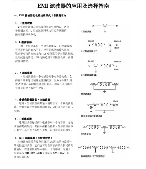
EMI滤波器的应用及选择指南一、EMI滤波器的电路结构形式(右图所示):1、C型滤波器C型滤波器由三端电容和穿心电容构成,适合于抑制高频。
C型滤波器两端均可视为低阻抗,接高阻抗源和负载。
2、L型滤波器由一个电感器和一个电容器组成。
这种滤波器可以提供高的输入阻抗,也可提供低的输入阻抗,取决于电路的安装方向。
LT电路适用于高阻抗负载,低阻抗源的情况。
LB电路适用于低阻抗负载,高阻抗源的情况。
3、π型滤波器π型滤波器由一个电感器两个电容器构成。
它的输入端和输出端都呈低阻抗性,因为元件比L型或C型多,故抑制性能要好的多。
但在开关电路中有时会出现“振铃”现象。
4、带瞬变抑制器的π型滤波器这种π型滤波器在其输入端增加了一个瞬变抑制器,它具有较好的高频抑制性能,同时可以防止电压尖峰。
5、T型滤波器这种滤波器包括两个电感器和一个电容器,它的两端都是高阻抗,其插入损耗性能和π型滤波器相似。
但它不易出现“振铃”现象,可用在开关电路中。
6、双T型滤波器(多级滤波器)多级滤波器是为源和负载都为低阻抗的电路设计的高性能滤波器,它们也可用在要求高插入损耗的其他情况。
在滤波器的输入端用一个电感器,有利于与美军标MIL-STD-461D(国军标GJB-151A)的测试装置匹配。
二、各种滤波电路的衰减特性:不同的滤波电路有着不同的滤波特性(见右图)。
一般而言,C 型电路的滤波衰减曲线较平坦,没有明显的拐点,适用于大多数电子设备;L 型电路Pi 型电路和T 型电路的滤波衰减曲线较C 型电路拐点明显,适用于抑制的干扰信号与有用信号频率接近的的场合。
但当工作频率为方波时,要注意这些电路的感性和容性器件的量值要选用恰当,避免一味追求滤波衰减性能,而把有用信号的波形部分衰减,导致设备工作反而不正常。
各种滤波电路滤波特性图一、 E MI 感性和容性器件的选择:滤波电容EMI 滤波器所用电容一般为穿芯式陶瓷电容,穿芯式的结构可有效防止高频信号在输入输出端之间直接耦合,且寄生电感小自谐振频率较高,这种同轴性的、低通高阻的设计组合,在1GHz 的频率范围内,可以提供高效的EMI 抑制。

批准: 日期: 第 1 页 共 3 页 连接仪器电源及被测负载电源的连接线;将待测样品的负载按要求接入。
分钟稳定后连接测试仪器数据线;当电脑通讯正常,打开电,打开测试界面。
测试完毕后,保存测试数据记录,关闭仪器及被测物电源。
电源端子骚扰电压测试: 线对电网的骚扰电压应不超过GB17743-2007表2a 限值;接收机、ENV216 人工电源网络(如下图); 连接人工电源网络后,连接接收机与人工电源网络的数据线; 键新建文件,然后点击Configure 配置,在limit (QP )选GB17743-2007 QP ,limit(AVG)选择(CE )GB17743-2007 AVG ,Antenna Conduction 键后点击SET 即可完成测试设定; Trace 追踪键,则接收机开始扫描测试; 11 10 12 13 14 15 16 17。
●电源,EUT电源和控制电缆 1选项和附件:●ECOUPLER 4 3相耦合/去耦网络440V 相到相16A连续/25A短时●IP4A EFT 容性耦合夹●EFT Kit 50/1000欧姆EFT测试工具●PDP8000 Differential HV Probe高压探头(8kV)●Current Probe 101 电流探头0.01V/A●LST-4510 用于磁场测试的1x1m线圈●PCD 121 耦合网络(对称数据和控制线)●PCD 126 耦合网络(非对称数据和控制线)3.1.4 静电放电测试系统KES4021 静电放电测试系统,30KV(Electrostic Discharge Simulator, including main unit, gun, IEC61000-4-2 CR unit, air and contact discharge tips)●电容:150Pf±10%●放电电阻:330Ω±10%●充电电阻:50-100MΩ●最大放电速率:20Hz●放电电压:接触放电8Kv,空气放电15Kv●放电电流:符合IEC 61000-4-2●保持时间:5秒●极性:+、-及+、-极性自动交替●触发方式:单次,及20次(或以下)3.2电磁干扰(EMI)实验设备1) 743半电波暗室(a)示意图(b)实例照片图3-14屏蔽半暗室743半电波暗室综合性能:暗室性能:(1) 屏蔽性能:依据标准EN50147-1, GB12190-90(2) 30MHz-1000MHz场地比对测试:以一个稳定的标准信号源于暗室完工后做一次窄频段比对校正,以SGS或者CCS标准暗室作为追溯的标准。
30-300MHz ±6dB;300-1000MHz ±4dB 项目内容:金属板可拆式半电波暗室外尺寸:7.2m×4.2m×3.4m L×W×H基本配置:气动屏蔽门:1×2m电源滤波器: 30A 220V 2只30A 110V 1只通风波导窗 30×30cm 2只0.3m高架地板,承重500kg/sqm地面接口箱 5只信号接口板1块(N×2 BNC×2,SMA×2)直径30×300mm 波导管 1根总电源控制箱 1套电源插座a.转桌中心 110VAC/15A x1 及220VAC/15A x1b. 天线塔附近:220VAC/15A x2c. 地板面上:220VAC/15A x2d.角度可调的固定式200W卤素灯在暗室內四个上角铁氧体介质板 12mm高密度板+导电铝箔(五面)铁氧体瓷砖(五面) SAMWHA SN-20手动转台台面式直径1米天线架固定高度(高度手动调节)转台上测试桌 1.2x1x0.8m 1张监控系统 1个松下470 Camera+1个14寸彩色Monitor主要配置:(1) 暗室屏蔽体:a.屏蔽体采用厚度为2mm的镀锌钢板。
前言电磁干扰的观念与防制﹐在国内已逐渐受到重视。
虽然目前国内并无严格管制电子产品的电磁干扰〔EMI〕﹐但由于欧美各国多已实施电磁干扰的要求﹐加上数字产品的普遍使用﹐对电磁干扰的要求已是刻不容缓的事情。
笔者由于啊作的关系﹐经常遇到许多产品已完成成品设计﹐因无法通过EMI测试﹐而使设计工程师花费许多时间和精力投入EMI的修改﹐由于属于事后的补救﹐往往投入许多时间与金钱﹐甚而影响了产品上市的时机2.正确的诊断要解决产品上的EMI问题﹐假设能在产品设计之初便加以考虑﹐那么可以节省事后再投入许多时间与金钱。
由于目前EMI Design-in的观念并不是十分普遍﹐而且由于事先的规划并不能保证其成品可以完全符合电磁干扰的测试在﹐所以如何正确的诊断EMI问题﹐对于设计工程师及EMI工程师是非常重要的。
事实上﹐我们如果把EMI当做一种疾病﹐当然平时的预防保养是很重要的﹐而一旦有疾病那么正确的诊断﹐才能得到快速的痊愈﹐没有正确的诊断﹐找不到病症的源头﹐往往事倍功半而拖延费时。
故在EMI的问题上﹐常常看到一个EMI有问题的产品﹐由于未能找到造成EMI问题的关键﹐花了许多时间﹐下了许多对策﹐却始终无法解决﹐其中亦不乏专业的EMI工程师。
以往谈到EMI往往强调对策方法﹐甚而视许多对策秘决或绝招﹐然而没有正确的诊断﹐而在产品上加了一大堆EMI抑制组件﹐其结果往往只会使EMI情况更糟。
笔者起初接触产品EMI对策修改时﹐会听到资深EMI工程师说把所有EMI对策拿掉﹐就可以通过测试。
初听以为是句玩笑话﹐如今回想这是很珍贵的经验谈。
而后亦听到许多EMI 工程师谈到类似的经验。
本文中将举出实际的例子﹐让读者更加了解EMI的对策观念。
一般提到如何解决EMI问题﹐大多说是case by case,当然从对策上而言﹐每一个产品的特性及电路板布线〔layout)情况不同﹐故无法用几套方法而解决所有EMI的问题﹐但是长久以来﹐我们一直想要把处理EMI问题并做适当的对策﹐另外也提供专业的EMI工程师一种参考方法。
EMC-EMI之综合解决方案引言概述:电磁兼容性(EMC)和电磁干扰(EMI)是现代电子设备设计和制造中的重要问题。
在一个复杂的电磁环境中,电子设备需要能够正常工作,而不会对其他设备或系统产生干扰。
为了解决这个问题,工程师们需要采取一系列综合的解决方案。
本文将介绍EMC-EMI综合解决方案的五个主要部分。
一、电磁兼容性设计1.1 电磁兼容性测试与分析:在设计阶段,工程师需要进行电磁兼容性测试和分析,以评估设备在电磁环境中的性能。
这包括测量设备的辐射和敏感性,以及分析设备的电磁兼容性问题。
1.2 电磁屏蔽设计:为了减少设备对外部电磁干扰的敏感性,工程师需要设计有效的电磁屏蔽。
这可以通过使用屏蔽材料、设计屏蔽结构和布线来实现。
1.3 地线和接地设计:良好的地线和接地设计是保证设备电磁兼容性的关键。
工程师需要注意地线的布线和连接,以减少电磁干扰的传导和辐射。
二、滤波器设计2.1 电源线滤波器:电源线滤波器可以有效地抑制电源线上的高频噪声和干扰。
工程师需要选择适当的滤波器类型和参数,以满足设备的EMI要求。
2.2 信号线滤波器:信号线滤波器可以减少信号线上的电磁干扰。
工程师需要根据信号频率和干扰源的特性选择合适的滤波器,并考虑滤波器对信号质量的影响。
2.3 模块化滤波器设计:对于大型系统或模块化设备,工程师可以设计模块化滤波器来简化滤波器的安装和维护。
这可以提高设备的可靠性和可维护性。
三、接地和屏蔽技术3.1 接地系统设计:良好的接地系统可以减少设备的地线回路干扰和地线回路噪声。
工程师需要设计合适的接地系统,包括接地电极的布置和连接。
3.2 屏蔽技术:除了电磁屏蔽设计外,工程师还需要考虑其他屏蔽技术,如屏蔽罩、屏蔽盒和屏蔽涂料。
这些技术可以进一步减少设备的辐射和敏感性。
3.3 防静电设计:静电会对电子设备的性能和可靠性产生负面影响。
工程师需要采取防静电设计措施,如使用防静电材料和接地技术,以减少静电干扰和损害。
EMI电源滤波器设计与测试
EMI(电磁干扰)电源滤波器是用于减少电源中的噪声和电磁干扰的一种装置。
在电源系统中,由于电源设备的运行,会产生电磁干扰并向电源线路传播。
这些干扰信号可能会影响其他设备的正常运行,因此需要采取措施来减少这些干扰。
首先,需要确定滤波器的频率范围。
根据要滤除的干扰信号的频率范围,可以选择适当的滤波器类型。
常见的滤波器类型包括:低通滤波器、带通滤波器和带阻滤波器。
其次,需要选择合适的滤波器参数。
滤波器参数包括:滤波器的截止频率、阻抗特性和衰减特性等。
这些参数的选择需要根据具体的应用需求和电源系统的特点来确定。
然后,需要进行EMI电源滤波器的设计。
可以使用模拟电路设计软件进行电路设计和模拟仿真,以验证滤波器的性能。
设计时需要考虑电容和电感的选择、滤波器电路的布局和组成部分之间的连接方式等。
设计完成后,需要进行EMI电源滤波器的测试。
测试可以使用仪器设备来进行,如频谱分析仪、信号发生器和示波器等。
测试时需要验证滤波器的频率响应、衰减特性和滤波效果等。
在测试中,可以通过调整滤波器参数和组成部分,进一步优化滤波器的性能。
如果测试结果不理想,可以尝试采取其他设计方法或更换滤波器元件。
总之,EMI电源滤波器的设计与测试是一项复杂的工作,需要综合考虑多个因素。
通过合理的设计和精确的测试,可以实现对电源中噪声和电磁干扰的有效滤除,提高电源系统的稳定性和可靠性。
EMIRFI-US-10IntroductionElectromagnetic compatibility (EMC) is the ability of electrical/electronic equipment to operate in its installation environment while neither causing nor experiencing electromagnetic interference (EMI). EMI is any interferencewith normal equipment operation caused by abnormal energy entering the equipment either by conduction though wiring connections orby radiated wave reception. Radiated EMI is also called radio frequency interference (RFI). Conducted EMI is also called high frequency line noise.Codes and Standards in the USAIn the USA, there are no codes and standards that specifi cally and completely cover electromagnetic compatibility of adjustable frequency drives (AFDs).FCC Rules and RegulationsPart 15 of the Federal Communications Commission (FCC) rules and regulations covers unlicensed equipment that emits radio frequency energy. Part 15 would apply to any AFD asan “incidental radiator.” The operation of any equipment covered by Part 15 is subject to the general conditions of operation listed under paragraph 15.5. The essential requirements of 15.5 are that the equipment must not interfere with any licensed broadcast, navigation or safety services and must accept any interference caused by other equipment. Under Part 15.13, the manufacturerof an incidental radiator “shall employ good engineering practices to minimize the risk of harmful interference.”Microprocessor controlled AFDs are also covered by FCC Part 15 as “digital devices.”As commercial or industrial equipment, AFDs are “exempted devices … subject only tothe general conditions of operation in 15.5 [described above]…” However, the FCC strongly recommends that “the manufacturer of an exempted device endeavor to have the device meet the specifi c technical standards [of Part 15].”Part 15 lists limits for radio frequency voltage conducted to the public utility power lines by digital devices. The range of frequencies covered is 0.15 to 30 MHz. Part 15 also lists limits for he fi eld strength of radiated emissions from digital devices. The range of frequencies covered is 30 MHz and above. At frequencies lower than the radio frequencies regulated by the FCC, voltages conducted to the power lines would be considered to be harmonic distortion voltages. Harmonic distortion issues are covered by IEEE Standard 519.FCC information and documents are availableat and/or links from to the Government Printing Offi ce web site. Evaluating a Drive as an FCC Part 15 “Digital Device”A drive’s microprocessor is not likely to be a signifi cant source of EMI. The most signifi cant potential source of EMI and RFI in a drive is the power switching circuitry. This potential is largely unrelated to the design of the microprocessor or other type of control circuitry. EMI is generated in a drive by switching the output terminals back and forth between the positive and negative sides of the DC bus to synthesize an AC output waveform. Each time the output transistor switches operate, the terminal voltage jumps (in a 480V drive) from 650 volts of one polarity to 650 volts of the opposite polarity. This nearly instantaneous voltage change has the potential to generate a signifi cant amount of radio frequency energy. Evaluating the drive as a microprocessor controlled “digital device” does not correctly target the most signifi cant source of EMI. Requiring a Drive to Meet the FCC RequirementsSince the applicable requirements are not very specifi c or restrictive, almost any drive couldbe said to meet the requirements of Part 15 without actually providing a signifi cant level of electromagnetic fi ltration.A drive could be required to meet the conducted and radiated emission limits listed in Part 15 for a Class A or ClassB digital device, but Part 15 does not contain or specify a testing procedure that is designed for use with drives. Without specifying a suitable testing procedure, any declaration that a drive meets the specifi ed limits might be suspect.The conducted emission limits listed in Part 15 were revised in 2002 to “harmonize our domestic requirements with the international standards developed by the International Electrotechnical Commission (IEC), International SpecialCommittee on Radio Interference (CISPR).” (See FCC 02-157). The CISPR 11 standard provides a suitable test procedure for testing drives to verify conformance with these limits.The radiated emission limits specifi ed by CISPR 22 are lower than the limits listed in Part 15. Accordingly, in 2003, Part 15 was revised to include 15.109(g):“As an alternative to the radiated emission limits shown in paragraphs (a) and (b) of this section, digital devices may be shown to comply with … (CISPR) Pub. 22 (1997)…” (See FCC DA 03-3848).CISPR 22 covers digital devices while CISPR 11covers industrial scientifi c and medical equipment.The U.S. Food and Drug Administrationencourages manufacturers of electromedicalequipment to use CISPR 11.EU Council Directives In the European Economic Community, the EU Council Directives set standards for variousproducts. Many of these standards are derivedfrom standards written by the International Electrotechnical Commission (IEC). The EMC Product Standard for Power Drive Systems, EN 61800-3 (or IEC 61800-3) is used as themain standard for variable speed drives. Thisstandard contains test procedures that are specifi cally suitable for drives and the standard is quite comprehensive. It covers both the drive’s electromagnetic emissions and its immunity from received emissions.IEC 61800-3 Defi nesTwo Installation EnvironmentsFirst Environment “The First Environment includes domesticpremises. It also includes establishments directlyconnected without intermediate transformer to alow-voltage power supply network which suppliesbuildings used for domestic purposes.”Tel: (800) 752-0696E M I RF I -U S -10 E f f e c t i v e : 5/16/05 ©2005 A B B I n c . S p e c i fi c a t i o n s s u b j e c t t o c h a n g e w i t h o u t n o t i c e .EMIRFI-US-10Second Environment“Second Environment includes all establishments other than those directly connected to a low-voltage power supply network which supplies buildings used for domestic purposes.”IEC 61800-3 Defi nes Sale or Distribution toTwo Levels of Customer CompetenceUnrestricted Distribution“Unrestricted distribution is a mode of salesdistribution in which the supply of equipment is not dependent on the EMC competence of the customer or user for the application of drives.”Restricted Distribution“Restricted distribution is a mode of salesdistribution in which the manufacturer restricts the supply of equipment to suppliers, customers or users who separately or jointly have technicalcompetence in the EMC requirements of theapplication of drives.” The installer must install thedrive in conformance with the instructions providedin the installation manual.Additional InformationAdditional information is available in two ABB publications:Technical Guide No. 2 EU Council Directives andAdjustable Speed Electrical Power Drive SystemTechnical Guide No.3 EMC Compliant Installation and Confi guration for a Power Drive System Recommendations to Specifi ers For drives with the most comprehensive electromagnetic compatibility, specifi ers should require drives to meet the IEC 61800-3 EMC standards and emission limits for Restricted Distribution and installation in theFirst Environment. Manuals should be required to include instructions for installing the driveequipment so that it meets the specifi ed emissionlimits as installed .Drives that meet the above requirements will typically meet the technical requirements of FCC Part 15 including the emission limits for a Class Adigital device.Tel: (800) 215-3006。
EMI测试整改和方法总结1实例水平与垂直读值的差异EMI 辐射测试整改和方法总结一.文章写得不错,值得推荐,这本书《 EMC 电磁兼容设计与测试案例分析》(第 2 版)也不错可以看看,呵呵关于电磁干扰的对策,许多刚接触的工程师往往面临一个问题,虽然看了不少对策的书籍,但是却不知要用书中的那些方法来解决产品的 EMI 问题。
这是一个很实际的问题,看别人修改似乎没什么困难,对策加了噪声便能适当的降低,而自己修改时下了一大堆对策,找了一大堆的问题点,却总不能有效地降低噪声。
事实上,这往往也是 EMI 修改最耗时间的地方,笔者把一些基本的判断方法做详细的介绍,以提供刚入门或正面临EMI 困扰问题的读者参考,整理了一些原则与判断技巧,希望能够对读者有帮助。
二. 水平、垂直判断技巧 EMI 的测试接收天线分为水平与垂直二个极化,亦即要分别测试记录此二个天线方向的最大读值,噪声必须要在天线为水平及垂直测量时皆能符合规格,测量天线要测量量水平及垂直二个方向,除了要记录到噪声最大时的读值外,也能显示出噪声的特性,由这个特性的显示,我们可初步判断造成 EMI 问题的重点,对于细部的诊断是很有帮助的,通常这个方法是很容易为修改对策人员所忽略。
在本期的分析中,笔者要介绍几种EMI 的判图技巧,也就是如何从静态的频谱分析仪所得到的噪声频谱图做初步的分析,另外也会介绍一般对策修改人员最常用的一些动态分析技巧。
许多工程师常常花了许多时间与精神,却感觉无法掌握到重点,可能就是缺乏基本分析的技巧,在噪声的判断上有一些混淆,如果能够掌握一些分析方法,可以节省不少对策的时间。
这里所提的一些方法,一直被不少资深的 EMI 工程师视为秘诀,因为其中往往是累积了多年的心得与经验才体悟出来的方法,而这些方法通常都是非常有效的。
射天线接收天线1. 这是 Modem &Telepho ne 的产品,读者可以很明显地看出来,天线水平时的噪声和垂直时的噪声有很大的差异,那么这其中代表了什么意义呢?分析讨论要清楚的认识这个问题,首先必须要了解天线的基本理论,我们先假设发射与接收天线皆为偶极天线。