企业培训-NOKIA 手机测试系统培训教材 精品
- 格式:ppt
- 大小:2.35 MB
- 文档页数:40


83080 Receiver Architectures and Synchronizationin Digital CommunicationsPractical RF Architectures for GSM and WCDMA Mobile TerminalsMobile Generations•1st generation systems, analog•NMT, AMPS, TACS•2nd generation systems, digital•GSM, IS-136 TDMA, IS-95 CDMA, PDC•3rd generation systems, digital wide band•WCDMA standards have been prepared by ETSI (Europe), ARIB (Japan), TIA (USA),...•3GPP1is a joint project that combines all proposals into one standard•Harmonized standard includes three modes•Direct sequence mode based on 3GPP (UTRA2/FDD)•Multi carrier mode based on CDMA2000 (USA proposal)•TDD mode based on 3GPP (UTRA/TDD)1) 3GPP = 3rd Generation Partnership Project2) UTRA = Universal Terrestrial Radio AccessMain Drivers for RF Architecture Design •Cost, Size, Power consumption•System complexity, time to marketComponent count in GSM RF501001502002503003504004505001994199619982000Design Process -time to market Req Spec's Req Spec's Applications Applications System Design System Design RF-, A/ASIC DesignRF-, A/ASIC Design Mfg ramp-up Mfg ramp-up Integration Integration HW, PCB, pkgHW, PCB, pkgMech. DesignMech. Design Concepts Concepts D/ASIC Design D/ASIC Design DSP, MCU SW designDSP, MCU SW designCritical Interface:from system design to detailed design Critical Interface:from detailed design to integrationGSM Specifications for Receiver•Bad frame indication performance•Sensitivity•Usable receiver input level range•Co -channel rejection•Adjacent channel rejection (selectivity)•Intermodulation rejection•Blocking and spurious response•AM suppressionExample of sensitivity specificationTable 1: Reference sensitivity performanceGSM 900Type of Propagation conditionschannel static TU50TU50RA250HT100(no FH)(ideal FH)(no FH)(no FH) FACCH/H(FER)0.1 % 6.9 % 6.9 % 5.7 %10.0 %FACCH/F(FER)0.1 %8.0 % 3.8 % 3.4 % 6.3 %SDCCH(FER)0.1 %13 %8 % 8 %12 %RACH(FER)0.5 %13 %13 %12 %13 %SCH(FER) 1 %16 %16 %15 %16 %TCH/F9.6 & H4.8(BER)10-50.5 %0.4 %0.1 %0.7 %TCH/F4.8(BER)-10-410-410-410-4TCH/F2.4(BER)-210-410-510-510-5TCH/H2.4(BER)-10-410-410-410-4TCH/FS(FER)0.1α%6α%3α%2α%7α %class Ib (RBER)0.4/α %0.4/α %0.3/α%0.2/α %0.5/α %class II (RBER)2%8%8%7%9% TCH/HS(FER)0.025 % 4.1 % 4.1 % 4.1 % 4.5 %class Ib (RBER, BFI=0)0.001 %0.36 %0.36 %0.28 %0.56 %class II (RBER, BFI=0)0.72 % 6.9 % 6.9 % 6.8 %7.6 %(UFR)0.048 % 5.6 % 5.6 % 5.0 %7.5 % class Ib (RBER,(BFI or UFI)=0)0.001 %0.24 %0.24 %0.21 %0.32 %(EVSIDR)0.06 % 6.8 % 6.8 % 6.0 %9.2 %(RBER, SID=2 and (BFI or UFI)=0)0.001 %0.01 %0.01 %0.01 %0.02 %(ESIDR)0.01 % 3.0 % 3.0 % 3.2 % 3.4 %(RBER, SID=1 or SID=2)0.003 %0.3 %0.3 %0.21 %0.42 %How to convert system specificationsto RF design parameters ?•From the bit error rate (BER) requirement of the whole phone we can derive secondary specifications for the radio section (Gain, Signal to Noise ratio, Linearity)•System specification and detector implementation define the required S/N ratio•GSM needs 8…9 dB S/N (number includes some implementation margin 2…3 dB)Radio section Detector BERC/N -15 dBm...-102 dBmSensitivityf 0S/N =9 dBNF = P s + 174 dBm -10 log B -S/NwhereB is equivalent noise bandwidth of the receiverP s is reference sensitivity levelFor GSM 900 MHz P s = -102 dBm -> NF = 10 dBSignal must be 9 dB above noise floor, sorequirement for receiver noise figure (NF) isPowerSensitivity and Selectivity •Cascaded noise figure•NF = 10 log F, where NF is noise figure and F is noise factor•F = F1+ (F2-1)/G1+ (F3-1)/G1G2+ … + (F n-1)/ G1G2…G n-1•RF section must have enough gain to provide adequate signal level for A/D converter•Minimum input level is -102 dBm -> 1.8 uV @ 50 ohm. If we need for example 100 mV at A/D converter input, voltage gain needs to be20log(100mV/1.8uV) = 95 dBF 1 F 2G1 G2FSelectivity•Before detector interfering signals need to be filtered so that S/N is adequate•This attenuation is split between IF filter, analog BB filter and digital filter after A/D•Digital filtering at baseband would be cost effective but then A/D coverter must be able to handle wider dynamic range (typical A/D resolution 10 (12)bits)•Distribution of gain and selectivity affects also linearity requirement of the analog part•If interfering signal is for example -43 dBm -> 5 mV @ 50 ohm and we amplify that 95 dB the signal level would be 280 V !Microsoft ExcelWorksheet•Local oscillator (LO) phase noise has effect both on sensitivity and selectivity •Phase noise may pass through mixer and degrade sensitivity different ways1) Noise at IF leaks directly into mixer IF port 2) Noise at RF leaks directly into mixer RF port3) Noise at the distance of IF from the RX-frequency mixes with RX and appears in the mixer IF port4) Noise at the distance of IF from the LO-frequency mixes with LO and appears in the mixer IF portIF IFIFRX IF4)4)3)2)1)RXIFLO•LO mixes both with wantedsignal and interfering signal•LO spectrum shifts to IFLO RX InterferenceIFIF•Usually selectivity sets most difficult requirement for VCO phase noise •Example GSM 900 MHz handportable:•wanted signal -102 dBm + 3 dB = -99 dBm•blocking signal -43 dBm @ 600 kHz offset•typical values S/N = 9 dB, noise BW = 200 kHz•Phase noise = -99-(-43)-10 log 200000 -9 = -118dBc/Hz (600 kHz)Receiver Architectures •Heterodyne+ flexibility, achievable component specifications+ standard components available-spurious responses•IF Sampling+ no need for I/Q mixer-requires better A/D converter•Homodyne (direct conversion)+ simplest architecture+ no IF filters, advantage especially in multiband/multisystem phones -very difficult to implementGSM Receiver Principles•GMSK modulation has no AM component that carries information •However the equalizer requires real time amplitude information to be able to correct the multipath propagation→Most common solution is linear receiver that provides in-phase (I) and quadrature (Q) signals for the baseband→Non linear (limiting) receiver possible, if it can provide amplitude information for the equalizerLimiting Receiver in GSM•Relaxes AGC and A/D requirements•High level interferers must be low enough before limiter-> requires good IF filters•Can handle fast amplitude changes without saturation•Mixing products in nonlinear circuits can cause spurious responses if they fall at IF or RX frequency •Usually low order products are the most important•Some examples of spurious responses in superheterodyne receiver with high side LO injection2LOIFIFf SPURLO2f SPURHalf IF: 2f LO -2f SPUR = f IFLOIFIFimageWanted signal Image: f SPUR -f LO = f IF•In full duplex systems the high level TX signal causes more spurious responses •If TX leaks to RX mixer it mixes directly with spurious signal: f SPUR -f TX = f IF •Mixing can also take place in power amplifier: 2f TX -f SPUR = f RX LOIFIFTXf SPURf SPURLO2TXTXf RX2f TX -f SPURf SPURfSPURf TXChoosing IF frequency•Spurious response requirements•Image should be at relatively quiet band•Usually IF/2 spurious should not be in RX band -> first IF > 2 * operating band•TX + IF should not fall in RX band (on the other hand we can use TX+ IF = RX)•IF filter availability, size and cost•71 MHz is most popular GSM IF at the moment•Higher frequency SAW filter is smaller but stopband attenuation is notas good•LO frequency•lower frequency is slightly easier to implement. On the other hand inmobile TX band is below RX and LO may be too close to TX band withlow side injection•Amount of oscillators•Use same oscillator for RX and TX if possible•harmonics of the oscillators should not fall in RX bandDuplexing Techniques•Uplink and downlink signals can be separated using different frequency or different time slot •RX and TX use same frequency but different time slot •-> Time Division Duplex (TDD)•RX and TX are on simultaneously but use different frequency •-> Frequency Division Duplex (FDD)•GSM can use either switch or duplexer•WCDMA must use a duplexer (option for TDD in the spec.)TX RXRXTXDuplexing Issues•Using a duplex filter in GSM may be feasible if RF archtecture is such that also TX needs good filtering•If a simple high pass filter is adquate in TX, lower cost and size can be achieved with a switch and separate filters•Typically swithch and filters are combined in a ceramic module•In GSM system receive and transmit functions occur in different time slots →Isolation between TX and RX is not a concern•High level circuit integration possible•Common blocks for RX and TX possible, e.g. synthesizer (frequency canbe shifted between RX and TX time slots)•Less spurious responses in the RXAutomatic Gain Control (AGC)•With AGC the average signal level at the A/D converter input is kept almost constant•Trade off between AGC and A/D converter dynamic range•In GSM phone reports received signal strength and +1 dB relative measurement accuracy is required from -110 dBm to -48 dBm•In IS-95 CDMA the TX power must follow received signal strength: Pout = -Pin -76 dBm at the input range -104 dBm to -25 dBm (open loop power control, accuracy requirement +9.5 dB)•In CDMA RX and TX gain controls should have similar temperature behaviorAGC Implementation•Accuracy and temperature compensation are easier to implement at IF and baseband•By adjusting front-end gain, AGC also provides a measure against intermodulation distortion at high signal levels•Often AGC is split between front-end and IF, for example20 (30)dB step in front-end and 60…80 dB at IFBaseband 935-960890-91513 1006-1031116 MHz13 MHz71 MHzQI+45ΣA/DD/ASuperheterodyne with IF sampling GSM 900 MHz÷2Baseband+45935-960890-91513I1006-103111671Q71 MHzQI+45ΣA/DD/ASuperheterodyne GSM 900 MHzExample of a GSM Block DiagramBaseband+45935-960890-91513I890 -960QQI+45ΣA/DD/ADirect conversion GSM 900 MHz•LO leakage to the RX input causes DC-offset•LO leakage can not be filtered out and it may cause too high spurious emissions(limit in GSM specification is -57 dBm)•High level interference signals can couple to LO an cause LO pulling•RF part must be very linear because strong adjacent channel signals are notfiltered out until baseband•To meet all requirements mixer linearity and balance are essential•Can be much larger than a weak signal•DC offset is first measured without signal before RX burst•This information is then used to cancel offset just before detection•Direct conversion implemented in GSM by Alcatel and Nokia•RFIC vendors are developing direct conversion chipsets (Analog Devices)BBLNAMIXRF INLOCLK DSP A DA D •Balanced circuits and double LO frequency reduce interference coupling90 d e gGSM Data Services, HSCSD and GPRS •HSCSD & GPRS•HSCSD = High Speed Circuit Switched Data•GPRS = General Packet Radio Service•Different coding 9.6 kbit/s -> 14.4 kbit/s•More slots, for example 2 slots -> 28.8 kbit/s•Dynamic use of slots in GPRS•In multislot case receiver has less time to changetime channel -> synthesizer must be faster•Adjacent slots may have different amplitude ->more dynamic range needed because gain controlhas no time to adapttimeGSM Data Services, EDGE•In EDGE also modulation changes GMSK -> 8PSK•Not constant amplitude anymore, only linear receiver possible•EDGE has several coding schemes and fastest data speeds can only be achieved with very good signal to noiseconditions•Theoretical maximum 69 kbit/s per timeslot•AGC gain distribution important•LNA gain step should not be used as low levels as inbasic GSMGSM Radio Access in the Time Domain RXTX MONITOR Adjacent cell BCCH max. 6 pcs.01234567012345674.615 ms 01234567012345670123456701234567HSCSD RF• 2 + 2 slots or 3 +1 slots still leave some settling time between the slots•In dual slot operation with maximum timing advance the time between RX and TX slots is 577 µs -233 µs = 344 µs•It becomes difficult to achieve this with conventional synthesizer •Separate synthesizers for RX and TX•Fractional-N synthesizer•Use double frequency (synthesizer step 400kHz) and dividefor LO• 3 + 3 slots and higher the RX and TX overlap and whole RF system design must be different including two synthesizers,duplex filter and high isolation between TX and RXSpread-Spectrum Basics•Spectrum is spread using a code that is independent of the information signal•Bandwidth used in spread spectrum transmission is typically at least 100 times wider than the information signal bandwidth•WCDMA uses direct sequence spreading where a pseudo-random code is directly combined to the signal•Users are separated by different codes•Bits in the spreading code are called chipstime timecode codeGSM WCDMAfrequency frequencyMobile Radio Channel•Multipath propagation (frequency selective fading)•Shadowing•Doppler shift→linear time-variant channelSignallevelTimeMobile Receiver•In GSM training sequence is used to estimate the impulse response of the radio channel•This information is necessary to equalize the user bits on a burst by burst basis•CDMA chip rate is typically greater than flat fading BW of the channel and multipath components appear like uncorrelated noise -> no equalizer is needed•RAKE receiver combines time shifted versions of the original signal •One finger is assigned for the direct signal, another for the reflectedsignal•Fingers in RAKE receiver can also be used for soft handoff•One finger is assigned for new base station while another still listens the old BS•RAKE receiver in implemented in digital baseband and it does not require any special functionality in RF part -> Receiver can be implemented with similar blocks as current GSM receiverCDMA System Parameters•IS-95 CDMA•Frequency bands•Cellular band (AMPS): TX 824…849, RX 869…894 MHz•PCS1900: TX 1850...1910, RX 1930...1990 MHz•Carrier spacing 1.25 MHz, 64 Walsh codes•Chip rate 1.2288 Mchip/s•WCDMA•Frequency bands•UTRA FDD (Europe & Asia): TX 1920…1980 MHz , RX 2110…2170 MHz •Carrier spacing 5.00 MHz•Chip rate 3.84 Mchips/s (first proposal 4.096 Mchips/s)Receiver requirements•Sensitivity requirement is -117 dBm @ 12.2 kbps user data rate •Changing user bit rate changes processing gain (PG) and also sensitivity level•PG = 10 log (3.84Mcps/user symbol rate)•Selectivity requirement is defined as RX filter attenuation at adjacent channel compared to wanted channel, spec is 33 dB, interferer crest factor not defined yetNoise floor Wanted signalNoise floor Wanted signalGSMWCDMARX Design issues•Full duplex operation•TX noise at RX band must be attenuated•A good duplexer is relatively large and expensive component •High chiprate•Wide BW in baseband -> higher current consumption•Wide band IF filters -> higher lossWCDMA RX Design Issues•Linear modulation -> limitting receiver not possible•In full duplex system TX noise at RX band may desense receiver•If we require that TX is not decreasing RXsensitivity, noise at RX input must below thermalnoise floor (-174 dBm/Hz)•Even if TX chain is relatively low noise, about 40dB attenuation is needed in duplexer•Wider band compared to GSM increases slightly filter losses and current consumptionVariable duplex separation•In WCDMA specification there is an option to use variable duplex separation•This means that receiver and transmitter channels can be selected freely and distance between RX and TX center frequency is variable •In current situation where operators have only two or three channels this option is not useful but if more spectrum becomes available it makes spectrum allocation more flexible•In superheterodyne receive variable duplex separation increases number of spurious responses dramatically and makes the calculation complex•With direct conversion architecture independent RX and TX frequencies are relatively easy to implementDirect Conversion Receiver in WCDMA•Integration level •Image suppression 90oDADA•DC offsets•Envelope distortion•Flicker noiseDSPDirect conversion problems in CDMA•No idle time slots for cancellation•Highpass filtering possible (dc block in thesignal path or servo feedback)•Slow transients•Large component values•Long-term average subtracted from signal•DSP controls analog offset•Digital methods•Typically for offsets 10-50 % depending onalgorithm•Own TX interference•Leakage through duplex filter and to RXVCO•TX modulation at mixer output•Double VCO frequency f=4 GHz anddifferential circuits reduce coupling•Envelope distortion•2nd-order nonlinearity•BALANCING•Mixer and first stages of baseband critical•Interference sources: all radio channels containing AM •Variable (non-constant) envelope in digital modulation–QPSK, QAM•TDMA (GSM)•TDD (WCDMA)•Analog baseband processing•Mixer is a part of the demodulator•I/Q balance•Offsets•Gain control•Time constant critical inside offset compensation loop•Techniques to maintain the same offset with different gain values •Flicker noise•Critical in direct conversion•Linearity & power consumption limits gain at RF•Smaller relative contribution in wide-band systemIntegrating WCDMA Receiver•Most functions can already be integarated•Most difficult blocks are•Front end RF filters•Tank circuit in VCO•Reference oscillator, at least crystal is external•Small size & smaller parasitics•Better matching•Low cost in mass productionSingle-Chip Integration •High-speed clock and digitalsignals on the same chip withRX front-end•Coupling through substrateand interconnections•Transmitter power and noiseon RX band•Differential RF•Double VCO frequency DALO CLKPAComponent Technologies •RF part of a GSM phone includes typically following blocks •One RF ASIC including RX, synthesizer(s) and TX•Power amplifier•VCO module•TCXO module•Front end switch•SAW filters (RX front end filter may be on the switch module)•Some passive components•In WCDMA RX and TX are likely to be on separate chipsComponent Technologies, RFIC •BiCMOS process is most suitable for RF ASIC design•Good RF performance•Easy to implement control logic and digital part in synthesizer •SiGe option increases ft•Main advantage of higher speed process is lower power consumption •Packages are typically ball grid arrays (BGA) with pin count up to 100•Power amplifier technologies•HBT GaAs (most popular today)•Silicon MOS•GaAs FET•Silicon bipolar•InP and InGaP are promising some performance improvement over GaAs HBTComponent Technologies, Filters andSwitches•Filter technology has been changing from ceramic to surface acustic wave (SAW)•Bulk Acoustic Wave (BAW) filters would give even smaller size and some integration possibilities•BAW technology is more difficult to implement than SAW beacause also material thickness should be controlled extremely accurately•Switches are used in front end so performance is very important because it directly effects the total receiver performance•GaAs FET and pin diode switches are used today•Micromechanical Switches (MEMS) would improve both insertion loss and isolation performance dramatically•MEMS linearity is also superior compared to electrical switches •Problems today are reliability and high control voltages。

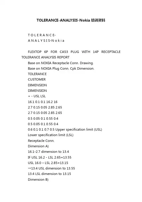
TOLERANCE-ANALYSIS-Nokia培训资料T O L E R A N C E-A N A L Y S I S-N o k i aFLEXTOP 6P FOR CA53 PLUG WITH 14P RECEPTACLE TOLERANCE ANALYSIS REPORTBase on NOKIA Receptacle Conn. Drawing.Base on NOKIA Plug Conn. Cpk Dimension.TOLERANCECUSTOMERDIMENSIONDIMENSION+ - USL LSL16.1 0.1 0.1 16.2 162.7 0.15 0.05 2.85 2.652.7 0.15 0.05 2.85 2.650.5 0.05 0.1 0.55 0.40.5 0.05 0.1 0.55 0.40.6 0.1 0.1 0.7 0.5 Upper specification limit (USL)Lower specification limit (LSL)Receptacle Conn.Dimension A)16.1-2.7 dimension to 13.4IF USL 16.2 - LSL 2.65=13.55USL 16.0 – LSL 2.85=13.15→13.4 USL dimension to 13.5513.4 LSL dimension to 13.15Dimension B)16.10+2.7 dimension to 18.8IF USL 16.2+ USL 2.85 =19.05USL 16.0 +LSL 2.65= 18.65→18.8 USL dimension to 19.0518.8 LSL dimension to 18.65Dimension D)Dimension A+0.5+0.5 dimension to 14.4IF USL 13.55+ USL 0.55+ USL 0.55 =14.65LSL 13.15 + LSL 0.40+ LSL 0.40 = 13.95TOLERANCECUSTOMERDIMENSIONDIMENSION+ - USL LSL13.50 0.15 0.15 13.65 13.3518.60 0.15 0.15 18.75 18.4514.50 0.05 0.05 14.55 14.450.200 0.03 0.03 0.23 0.17 Analysis A Dimension:The Rec. USL dimension to 13.55 -- The Plug LSL. Dimension to 13.35.→Analysis result is fail.The Rec. LSL dimension to 13.15 -- The Plug LSL. Dimension to13.35.→Analysis result is OK.The Rec. LSL dimension to 13.15 -- The Plug USL. Dimension to 13.65.→Analysis result is OK.The Rec. USL dimension to 13.55 -- The Plug USL. Dimension to 13.65.→Analysis result is OK.Analysis B Dimension:The Rec. USL dimension to 19.05 -- The Plug LSL. Dimension to 18..45.→Analysis result is OK.The Rec. LSL dimension to 18.65 -- The Plug LSL. Dimension to 18.45.→Analysis result is OK.The Rec. LSL dimension to 18.65 -- The Plug USL. Dimension to 18.75.→Analysis result is fail.The Rec. USL dimension to 19.05 -- The Plug USL. Dimension to 18.75.Analysis C Dimension:The Rec. Conn. Contact area dimension is 0.6±0.1The plug Conn. Contact area dimension is 0.2±0.03The Rec. USL dimension to 0.7 -- The Plug LSL. Dimension to 0.17.→Analysis result is OK.The Rec. LSL dimension to 0.6 -- The Plug LSL. Dimension to 0.17.→Analysis result is OK.The Rec. LSL dimension to 0.6 -- The Plug USL. Dimension to 0.23.→Analysis result is OK.The Rec. USL dimension to 0.7 -- The Plug USL. Dimension to 0.23.→Analysis result is OK.Analysis D Dimension:The Rec. USL dimension to 14.65 -- The Plug LSL. Dimension to 14..45. →Analysis result is fail.The Rec. LSL dimension to 13.95 -- The Plug LSL. Dimension to 14.45. →Analysis result is OK.The Rec. LSL dimension to 13.95 -- The Plug USL. Dimension to 14.55. →Analysis result is OK.The Rec. USL dimension to 14.65 -- The Plug USL. Dimension to 14.55. →Analysis result is fail.TOLERANCECUSTOMERDIMENSIONDIMENSION+ - USL LSL2.9 0.15 0.053.05 2.85TOLERANCECUSTOMERDIMENSIONDIMENSION+ - USL LSL2.90 0.08 0.08 2.98 2.82The Rec. USL dimension to 3.05 -- The Plug LSL. Dimension to 2.82.→Analysis result is OK.The Rec. LSL dimension to 2.85 -- The Plug LSL. Dimension to 2.82.→Analysis result is OK.The Rec. LSL dimension to 2.85 -- The Plug USL. Dimension to 2.98.→Analysis result is fail.The Rec. USL dimension to 3.05 -- The Plug USL. Dimension to 2.98.→Analysis result is OK.SUGGESTSuggest modify the receptacle and plug dimension tolerance RECETPACLE CONN.Suggest: 2.7 + 0.15/-0.05 change to 2.7+0.15/-02.7 USL dimension to 2.852.7 LSL dimension to 2.70Suggest: 16.1± 0.1change to 16.1+0/-0.116.1 USL dimension to 16.116.1 LSL dimension to 16.0Suggest: 0.5 ± 0.1change to 0.5 +0/-0.10.50 USL dimension to 0.500.50 LSL dimension to 0.40PLUG CONN.Suggest: 13.50 ± 0.15change to 13.50+0.15/-02.7 USL dimension to 2.852.7 LSL dimension to 2.70Suggest: 18.60 ± 0.15chan ge to18.60+0/-0.1518.60 USL dimension to 18.6018.60 LSL dimension to 18.45Dimension A)16.1-2.7 dimension to 13.4IF USL 16.1 - LSL 2.70=13.40USL 16.0 – LSL 2.85=13.15→13.4 USL dimension to 13.4013.4 LSL dimension to 13.15Dimension B)16.10+2.7 dimension to 18.8IF USL 16.1+ USL 2.85 =18.95USL 16.0 +LSL 2.65= 18.65→18.8 USL dimension to 18.9518.8 LSL dimension to 18.65Dimension D)Dimension A+0.5+0.5 dimension to 14.4IF USL 13.40+ USL 0.50+ USL 0.50 =14.40LSL 13.15 + LSL 0.40+ LSL 0.40 = 13.95→14.4 USL dimension to 14.4014.4 LSL dimension to 13.95Analysis A Dimension:The Rec. USL dimension to 13.40 -- The Plug LSL. Dimension to 13.50.→Analysis result is OK.The Rec. LSL dimension to 13.15 -- The Plug LSL. Dimension to13.50.→Analysis re sult is OK.The Rec. LSL dimension to 13.15 -- The Plug USL. Dimension to 13.65.→Analysis result is OK.The Rec. USL dimension to 13.40 -- The Plug USL. Dimension to 13.65.→Analysis result is OK.Analysis B Dimension:The Rec. USL dimension to 18..95 -- The Plug LSL. Dimension to 18..45.→Analysis result is OK.The Rec. LSL dimension to 18.65 -- The Plug LSL. Dimension to 18.45.→Analysis result is OK.The Rec. LSL dimension to 18.65 -- The Plug USL. Dimension to 18.60.→Analysis result is OK.Analysis D Dimension:The Rec. USL dimension to 14.40 -- The Plug LSL. Dimension to 14..45.→Analysis result is OK.The Rec. LSL dimension to 13.95 -- The Plug LSL. Dimension to 14.45.→Analysis result is OK.The Rec. LSL dimension to 13.95 -- The Plug USL. Dimension to 14.55.→Analysis result is OK.The Rec. USL dimension to 14.40 -- The Plug USL. Dimension to 14.55.→Analysis result is OK.RECETPACLE CONN.Suggest: 2.9 + 0.15/-0.05 change to 2.9+0.15/-02.9 USL dimension to3.052.9 LSL dimension to 2.90PLUG CONN.Suggest: 2.90 ± 0.08change to 2.90+0./-0.082.9 USL dimension to 2.92.9 LSL dimension to 2.82The Rec. USL dimension to 3.05 -- The Plug LSL. Dimension to 2.82.→Analysis result is OK.The Rec. LSL dimension to 2.90 -- The Plug LSL. Dimension to 2.82.→An alysis result is OK.The Rec. LSL dimension to 2.90 -- The Plug USL. Dimensionto 2.90.→Analysis result is OK.The Rec. USL dimension to 3.05 -- The Plug USL. Dimension to 2.90.→Analysis result is OK.。

NOKIA BSS 概述BSS的主要作用是通过空中接口连接无线用户。
BSS子系统的核心是BSC,BSC连接BTS,通过BTS给MS提供无线接口,它的主要功能是:陆地信道管理配置和管理业务信道跳频控制寻呼BTS和MS功率控制空闲信道质量监视当前激活信道的质量和强度控制切换控制BTS和BSC和TC的维护提供到OMC和BTS和TC的接口BSS子系统中话音变换起重要作用的是TC(码型变换和速率适配器),它的主要功能是:进行传输编码功能提供MSC与BSC之间NO.7信令连接建立MSC与BSC之间X.25信道下行链路对每个信道功率控制的调整速率适配BSS子系统中重要的功能元件是BTS,它的主要功能是:将MS和BTS的测量报告统计到BSCMS和BTS之间的维护和同步监听来自MS的RACH速率适配无线信道编码和解码无线信道加密和解密执行跳频高斯最小移位键控采用相位的变化将数字信号转成模拟信号射频信号多路耦合接口将空闲业务信道的质量报告给BSC提供到BSC或到MS的接口OMCR是无线操作和维护中心,它的功能是:故障管理性能管理配置管理1、空中接口1)空中接口的作用是提供BSS和MS的连接,空中接口使用两种技术:TDMA(时分多址)FDMA(频分多址)TDMA帧分为TS0到TS7的八个时隙,由相同时隙组成BURST用于承载话音或信令,如果时间同步不好,会把自己的信息掉到其他时间段中,以防信息丢失2)DCS1800M在空中接口所用的频带:上行链路 1710MHZ——1785MHZ下行链路 1805MHZ——1880MHZ信道间隔 200KHZ双工间隔 95MHZ频带宽度 75MHZ频点号为512——885共374个频点3)信道物理信道:1个时隙就是1个物理信道,信道指连续TDMA帧的同一个时隙构成的组合逻辑信道:指物理信道所承载的信息,根据不同的种类、内容、功能分成不同的逻辑信道,包括:公共控制信道(CCCH)专用控制信道(DCCH)公共控制信道包括:广播信道组合(BCCH)分为频率校正信道(FCCH),同步信道(SCH),广播控制信道(BCCH)公共控制信道组合分为寻呼信道(PCH),允许接入信道(AGCH),随机接入信道(RACH)专用信道包括:SDCCH独立专用控制信道,SACCH慢速随路控制信道,FACCH快速随路控制信道,业务信道(TCH)4)突发序列(BURST)突发(BURST):一个时隙一次发送的内容称为一个突发,分为: NORMAL BURST:传送TCH、BCCH、CCCH、SDCCH、SACCH、、FACCH FCCH BURST:传送FCCHSYNCHRONIZATION BURST:传送SCHACCESS BURST:传送RACH5)帧结构复帧有两种:TCH复帧:由26TDMA帧组成信令复帧:由51TDMA帧组成超帧:26*51TDMA帧超高帧:2048*26*51TDMA帧TDMA帧号:0——2048*26*51-1,在一个超高帧内TDMA帧号是唯一的帧周期:一个TDMA帧周期是4.615MS,一个超高帧的周期是3小时28分53秒760毫秒3.RADIO PATH1)载频频率:上行频率 1710+0.2*N(N为频点号)下行频率 1805+0.2*N2)衰落:分为快衰落和慢衰落快衰落:由多径传输引起,分为选择性衰落和平衰落慢衰落:由阴影效应引起,解决方案:自适应功率控制选择性衰落:由信号反射引起,由于反射信号与直射信号的路程差大,码间干扰时延超过一个比特位时多径信号叠加,出现符号间干扰.解决方案:维特比均衡平衰落:从同一个的信号源发出的信号到达MS有直射的和反射的,时延忽略不计,幅度作矢量和,平衰落是由矢量和引起的衰落坑(矢量和低于灵敏度)解决方案:①跳频,分为基带跳频、射频跳频基带跳频:载频频点不变,同一话务由不同载频发送射频跳频:给每个载频分配多个频点,话务始终由同一载频发送②信道编码,采用A律13折线PCM编码话音编码,采用波形编码和特征编码相结合③交织,使不同BURST承载信息的重要程度相同④分集接收:两根天线接收信号合成最优分集天线距离4、DX200 BSCBSC功能:①无线资源管理,包括BCF、BTS、TRX管理ABIS信道排列释放信道测量的处理功率控制逻辑信道的管理②切换管理③跳频④BSC信令⑤加密⑥维护⑦测量报告⑧支持呼叫控制备板:MCUC:总线接口单元,控制主交换单元,控制SW1C,MCUC是1+1配置,算作BSC的主控单元ET5C:2M接口,主架两个,扩展架3个BCSU:信令处理CLOC:主架时钟CLAC:扩展架时钟SW1C:主交换单元WDDC:硬盘NOKIA ULTRASITE简介UL TRASITE是NOKIA公司比较新的一代产品,但我们现在还没有应用。

易兴通电子有限公司手机测试培训操作指南一、手机软件与升级管理二、手机RF(BT/FT/CIT)系统测试操作指南三、手机包装测试操作指引四、条码标签打印操作介绍五、生产&出货IMEI/MEID 号管理规定手机软件与升级管理1. 软件管理:1.1:软件管理是指对公司各机型的软件更新进行记录,及时将最新软件导入生产中及将旧软件进行归档以便日后查阅.1.2:软件接收:文控室负责(或测试工程师)接收提取客户提供各类软件及相关技术文档,同步发给相应部门。
并复制到公司指定服务器上保存并注明。
1.3:软件ECN 发行:工程文员或文控室收到客户软件,在项目经理或测试工程师指导下把相关软件ECN 电子档、纸档或邮件方式发行到各部门,同时将软件发行,各部按ECN 操作执行。
1.4:软件对照表更新:测试工程师收到文控发行软件,根据客户类型将客户软件对照表转换更新易兴通内部软件对照表发布相关使用部门,文控负责将最新软件对照表打印受控发行到各产线MMI 工位、品质检验人员、升级测试房,并将旧软件对照表收回存档。
1.5:软件执行:测试工程将收到的软件复制到下载PC 上,将下载软件平台工具调试好,准备量产下载。
1.6:软件功能确认:由工程师抽5PCS 对下载好软件机器进行功能全检,如功能都OK 软件将正式实行,工程、质量共同确认升级下载首件,如发现软件有Bug 将反馈给相关负责部门,直到问题有解决方案为此,否则不能正式上线。
2. 软件升级管理:升级硬件&软件准备:PC 加多口USB 接口、下载线、下载夹具、各机型升级工具、软件、操作说明注意事项。
2.1:软件归档量产操作:软件确认正确及功能确认OK 后将记录在‘软件对照表’中,记录软件的机型;版次;软件发行日期等信息,如特殊操作(易丰客户软硬三大件匹配关系应用,相关使用部门严格按照软件对照表匹配发料;易丰条码打印要求出货SN 号设计软件硬件代码,备料单严格按照实际软硬件匹配关系备料。

手机软件测试培训资料标题:手机软件测试培训资料随着移动互联网的迅速发展,手机软件测试变得越来越重要。
为了帮助测试人员更好地理解和掌握手机软件测试的技术和方法,本文提供了一系列的培训资料。
一、测试基础知识1、软件测试的定义和目的2、手机软件测试的特点和要求3、测试流程和测试计划4、测试用例设计和执行5、缺陷管理和报告二、测试技巧和方法1、黑盒测试技术2、白盒测试技术3、灰盒测试技术4、单元测试、集成测试和系统测试5、自动化测试工具和方法三、测试工具和环境1、模拟器和真机使用技巧2、测试管理工具和缺陷跟踪系统3、性能测试工具和指标4、安全测试工具和最佳实践5、跨平台测试工具和策略四、实践案例分析1、某知名社交App的测试流程和经验分享2、某知名电商App的测试策略和方法解析3、某知名视频App的测试技巧和工具介绍4、某知名游戏App的测试管理和自动化实践5、某知名金融App的安全测试和漏洞修复经验五、参考资料和推荐阅读1、软件测试经典著作介绍2、手机软件测试相关学术论文和报告3、知名博客和论坛资源推荐4、最新测试工具和技术发展趋势以上是本文提供的手机软件测试培训资料,希望能对大家有所帮助。
如果大家需要更深入的了解和培训,请参考相关文献或联系专业机构。
小米手机培训资料标题:小米手机深度解析与使用技巧培训资料一、引言随着科技的飞速发展,智能手机已经成为我们日常生活中不可或缺的一部分。
在这个市场中,小米手机凭借其创新的科技设计、强大的性能和出色的用户体验,赢得了全球消费者的喜爱。
本文将详细介绍小米手机的特点、功能和使用技巧,为读者提供一份全面的培训资料。
二、小米手机简介小米手机诞生于2010年,凭借其高品质和亲民的价格迅速赢得了市场份额。
近年来,小米在设计、性能和用户体验方面不断突破,已经成为全球领先的智能手机品牌之一。
小米手机的核心价值观是“为发烧而生”,致力于为消费者提供极致的手机体验。
三、小米手机特色功能1、高度定制的MIUI系统:小米手机搭载了基于Android系统深度定制的MIUI系统,针对中国消费者的使用习惯进行优化,提供了更智能、更便捷的手机体验。

诺基亚手机服务信息系统V2.0培训手册北京尚思科技有限公司VERSION 2.13.012007年11月一、培训目标1. 使培训人员能够清晰系统所涉及业务的流程;2. 使培训人员能够清晰系统所涉及的各种角色以及作用;3. 使培训人员能够熟练的使用系统;4. 使培训人员能够部分解决ASC在实际使用系统时所提出的问题。
二、培训所需资源1. 为了保证培训的效果,每位培训老师一次培训的人员应在5人以内;2. 培训人员每人一台计算机,以便进行系统操作练习;3. 培训人员计算机的操作系统最好为中文Win2000,中文Win98或中文WinXP也可以接受;4. 培训人员的计算机应该在同一局域网内,并且已经能够通过局域网互相访问;5. 培训人员每人一套培训材料;6. 培训时间暂定3天,根据培训效果适当延长,最长不超过5天。
三、培训内容1.系统的背景和作用1.1 背景随着NOKIA在中国手机业务的快速发展,NOKIA 手机的用户在迅速增加。
为了给NOKIA手机用户提供更加完善的服务,NOKIA在全国范围内建立了数量庞大的手机专卖店和授权服务中心。
与此同时,中国政府对于家电行业的服务规范也在不断加强,对相关的制造和销售企业进行了更加严格的管理和控制。
在这两方面因素的影响下,NOKIA需要不断完善对手机专卖店和授权服务中心的管理,而诺基亚手机服务信息系统正是其重要基础之一。
重新开发的诺基亚手机服务信息系统是在继承了原有系统优点的基础上,针对NOKIA目前服务管理的需要而设计开发的,它一定能够为NOKIA在中国的手机服务管理提供更加强有力的支持。
1.2 作用诺基亚手机服务信息系统的主要作用是帮助NOKIA加强对手机专卖店和授权服务中心服务的管理,同时也帮助手机专卖店和授权服务中心管理自己的各种服务。
从NOKIA的角度来看,诺基亚手机服务信息系统能够及时提供手机专卖店和授权服务中心的服务信息,增加NOKIA对手机专卖店和授权服务中心所提供服务的数量和质量的了解,为NOKIA对手机专卖店和授权服务中心的管理提供了可以信赖的数据基础。