sensoric_appnote14 Mechanical Dimensions – SensoriC Classic
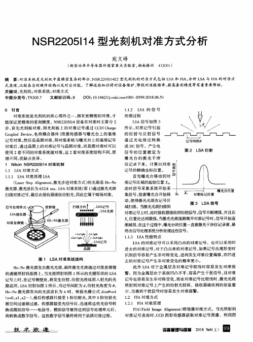
- 格式:pdf
- 大小:48.03 KB
- 文档页数:1

NAO机器人编程学习目录1、基本介绍 (1)1.1实体平台 (2)1.1.1运动 (2)1.1.2视觉 (2)1.1.3语音 (2)1.1.4触摸传感器和声纳测距仪 (3)1.1.5连接性 (3)1.1.6开源 (4)1.2特征参数 (4)2、Choregraphe软件 (5)2.1Choregraphe软件介绍 (5)2.2综合运用 (5)2.2.1连接机器人 (6)2.2.2程序编写 (6)机器人NAO是各种软、硬件巧妙结合的独特产物,由大量传感器、电机和软件构成,所有软件由专门设计的操作系统NAOqi来控制。
NAO虽然目前还尚未进入家庭,但已在教育界成为一颗耀眼的明星。
在70多个国家里,它走入中学和大学的信息技术和科技专业课堂,许多大学生借助NAO,以寓教于乐、学以致用的方式学习编程。
NAO也征服了一大批程序开发人员。
在他们眼里,NAO 是一个功能强大、具有惊人表现力的应用程序创建平台,可以让大量设想变为现实,由此开辟出程序开发的新天地,也为日后创作出面向大众的机器人铺平了道路。
1、基本介绍1.1实体平台NAO是一个身高58cm的可编程仿人机器人,内含以下构件:⑴拥有25个自由度的身体,主要元件为电机和电动制动器;⑵传感器系统,包括:2个摄像头、4个麦克风、声纳测距仪、2套红外线接收器和发送器、1个惯性器件板、9个触摸传感器和8个压力传感器;⑶多种交流设备,包括语音合成器、LED灯及2个高保真扬声器;⑷英特尔ATOM 1.6 GHz处理器(位于头部),运行Linux内核;⑸第二个CPU位于躯干;⑹27.6瓦时电池,根据使用情况,可为NAO提供超过1.5个小时的自主动力。
1.1.1运动1.1.1.1全方位行走NAO行走使用的是一个简单的动态模型(直线倒立摆)和二次规划,通过关节传感器反馈的信息保持稳定,保证行走的鲁棒性,免受小干扰,并可吸收躯干在正向和侧向平面上的摆动。
NAO 可在多种地面上行走,如地毯、瓷砖地、木地板等,而且在行走过程中能够顺利地从一种地面走到另一种地面上。

NXP Semiconductors Document identifier: MIMXRT10601064EKBHUG User's Guide Rev. 0, 06/2020MIMXRT1060/1064 Evaluation Kit Board Hardware User's GuideContentsChapter 1 Introduction (3)1.1 Board overview (3)1.2 MIMXRT1060/1064 EVK contents (4)1.3 MIMXRT1060/1064 EVK board revision history (4)Chapter 2 Specifications (5)2.1 i.MX RT1060/1064 processor (7)2.2 Boot mode configurations (7)2.3 Power tree (8)2.4 SDRAM memory (11)2.5 SD card slot (11)2.6 Hyper flash (11)2.7 QSPI flash (11)2.8 Ethernet connector (12)2.9 USB PHY connector (12)2.10 Audio input/output connector (12)2.11 OpenSDA circuit (DAP-Link) (12)2.12 JTAG connector (12)2.13 Arduino expansion port (13)2.14 Camera module connector (14)2.15 User interface switch (14)2.16 Sensor (15)2.17 User interface LED indicator (15)2.18 LCD interface (15)Chapter 3 PCB information (16)Chapter 4 EVK design files (17)Chapter 5 EVK contents (18)Chapter 1IntroductionThis document describes MIMXRT1060/1064 Evaluation Kit (EVK) based on the i.MX RT1060/1064 processor from NXP Semiconductor. The document includes system setup, debugging, and provides detailed information on the overall design and usage of the EVK board from a hardware system.1.1Board overviewThis EVK board is a platform designed to showcase the commonly used features of the i.MX RT1060/1064 Processor in a small, low-cost package. The MIMXRT1060/1064 EVK board is an entry level development board that familiarizes the developer to the processor before investing on resources for specific designs.The features of the MIMXRT1060/1064 EVK board are listed in Board features.The features of the MIMXRT1060/1064 EVK board are listed in Table 1.Table 1.Board featuresProcessor NXP Processor MIMXRT1062DVL6AMIMXRT1064DVL6ADRAM Memory SDRAM 256 Mbit, 166 MHz IS42S16160J-6BLIDCDC MPS MP2144GJLDO UNION UM1550S-18UM1750S-00Mass Storage TF Card Slot64 Mbit Quad SPI flash512 Mbit Hyper flashDisplay Interface LCD connectorEthernet10/100 Mbit/s Ethernet connector. PHY chip: KSZ8081RNBUSB USB 2.0 OTG connectorUSB 2.0 host connectorAudio Connector 3.5 mm audio stereo headphone jackBoard-mounted microphoneLeft and right speaker out connectorsS/PDIF interface (unpopulated )Power Connector 5 V DC-jackDebug Connector JTAG 20-pin connector (SWD by default)OpenSDA with DAP-LinkSensor FXOS8700CQ: 6-Axis Ecompass (3-Axis Mag, 3-Axis Accel)(Some boards are unpopulated)Table continues on the next page...IntroductionTable 1.Board features (continued)Camera CMOS sensor interfaceCAN CAN bus connectorUser Interface Button ON/OFF, POR Reset, Reset, USER buttonLED Indicator Power Status, Reset, OpenSDA, USER LEDExpansion Port Arduino interfacePCB 3.937 inch x 5.9055 inch (10 cm x 15 cm), 4-layer board1.2MIMXRT1060/1064 EVK contentsThe MIMXRT1060/1064 EVK contains the following items:•MIMXRT1060/1064 EVK board•USB cable (Micro B)•Camera1.3MIMXRT1060/1064 EVK board revision historyEVK: Mass ProductChapter 2SpecificationsThis section provides detailed information about the electrical design and practical considerations of the EVK board. The document describes each block shown in Block diagram.The document describes each block shown in Figure 1.Figure 1.Block diagramThe overview of the MIMXRT1060 EVK board is shown in Figure 2 and Figure 3.Figure 2.Overview of the MIMXRT1060 EVK board (Front side)Figure 3.Overview of the MIMXRT1060 EVK board (Back side)2.1i.MX RT1060/1064 processorThe i.MX RT1060/1064 is a new processor family featuring NXP advanced implementation of the Arm Cortex-M7 Core. It provides high CPU performance and best real-time response. i.MX RT1060/1064 provides various memory interfaces, including SDRAM, Raw NAND flash, NOR flash, SD/eMMC, Quad SPI, HyperBus, and a wide range of other interfaces for connecting peripherals, such as WLAN, Bluetooth™, GPS, displays, and camera sensors. i.MX RT1060/1064 has rich audio and video features, including LCD display, basic 2D graphics, camera interface, S/PDIF, and I2S audio interface.The i.MX RT1060/1064 applications processor can be used in areas such as industrial HMI, IoT, motor control, and home appliances. The flexibility of the architecture enables it to be used in a wide variety of other general embedded applications too. The i.MX RT processor provides all interfaces necessary to connect peripherals such as WLAN, Bluetooth™, GPS, camera sensors, and multiple displays.The more detail information about i.MX RT1060/1064 can be found in the Datasheet and Reference Manual.2.2Boot mode configurationsThe device has four boot modes (one is reserved for NXP use). The boot mode is selected based on the binary value stored in the internal BOOT_MODE register.Switch (SW7-3 and SW7-4) is used to select the boot mode on the MIMXRT1060/1064 EVK board.Table 2.Boot mode pin settingsBOOT_MODE[1:0] (SW7-3 SW7-4)BOOT TypeTable continues on the next page...Table 2.Boot mode pin settings (continued)00Boot From Fuses 01Serial Downloader 10Internal Boot 11ReservedTypically, the internal boot is selected for normal boot, which is configured by external BOOT_CFG GPIOs. Table 3 shows the typical Boot Mode and Boot Device settings.Table 3.Typical boot mode and boot device settings for RT1060SW7-1SW7-2SW7-3SW7-4Boot Device OFF ON ON OFF Hyper flash OFFOFF ON OFF QSPI flash ONOFFONOFFSD cardFor more information about boot mode configuration, see the System Boot chapter of the MIMXRT1060 Reference Manual .For more information about MIMXRT1060 EVK boot device selection and configuration, see the main board schematic .Table 4.Typical boot mode and boot device settings for RT1064SW7-1SW7-2SW7-3SW7-4Boot Device OFF OFF ON OFF QSPI flash ONOFFONOFFSD card2.3Power treeA DC 5 V external power supply is used to supply the MIMXRT1060/1064 EVK board at J2, and a slide switch SW1 is used to turn the Power ON/OFF. J41 and J9 is used to supply the EVK board.Table 5 lists different J1 jumper settings for different power supply.Table 5.Jumper settings for power supply Power Supply J1 Setting J21-2J93-4J415-6The power tree is shown in the following figure.Figure 4.Power treeThe power control logic of the MIMXRT1060/1064 EVK board is shown in the Figure 5.•SNVS is powered first and then PMIC_REQ_ON is switched on to enable external DC/DC to power up other power domains.•ON/OFF button is used to switch ON/OFF PMIC_REQ_ON to control power modes.•RESET button and WDOG output are used to reset the system power.Figure 5.Power control diagramThe power rails on the board are shown in Table 6.Table 6.Power railsTable continues on the next page...Table 6.Power rails (continued)2.4SDRAM memory256 Mbit, 166 MHz SDRAM (IS42S16160J-6BLI) is used on the EVK board.2.5SD card slotThere is an SD card slot (J39) on the MIMXRT1060/1064 EVK board. J39 is the Micro SD slot for USDHC1 interface. To boot from the SD card, the boot device switch (SW7) settings should be: ON, OFF, ON, OFF, as shown in Typical boot mode and boot device settings.2.6Hyper flashOn the MIMXRT1060/1064 EVK board, there is one 512 Mbit hyper flash device. To boot from the Hyper Flash, the boot device switch (SW7) settings should be: OFF, ON, ON, OFF, as shown in Table 3. By default, this hyper flash is disabled on the EVK. To enable the onboard hyper flash, update the following settings.1.Weld resistors: R356, R361 - R366.2.Removed 0Ωresistors: R153 - R158.The boot from hyper flash only supports RT1060.2.7QSPI flashA 64 Mbit QSPI flash is used on the MIMXRT1060/1064 EVK board. If the developer wants to boot from the QSPI flash, the boot device switch (SW7) settings should be: OFF, OFF, ON, OFF, as shown in Table 3. The QSPI flash is the default onboard flash.The boot from QSPI flash only supports RT1060.2.8Ethernet connectorThere are two Ethernet Mac controllers in the MIMXRT1060/1064 processor. The Ethernet subsystem of the MIMXRT1060/1064 EVK board is provided by the KSZ8081RNB 10/100 M Ethernet Transceiver (U16) and an RJ45 (J19) with integrated magnetic.2.9USB PHY connectorMIMXRT1060/1064 contains two integrated USB 2.0 PHYs capable of connecting USB host/device systems at:•USB low-speed (LS) rate of 1.5 Mbits/s•USB full-speed (FS) rate of 12 Mbits/s•USB 2.0 high-speed (HS) rate of 480 Mbits/s2.10Audio input/output connectorThe audio codec used on the MIMXRT1060/1064 EVK board is Wolfson’s low power, high-quality stereo codec, WM8960. The MIMXRT1060/1064 EVK board includes:•one headphone interface (J12)•one onboard MIC (P1)•two speaker interfaces (J16, J17)•S/PDIF interface (J14 and J18, DNP).J12 is a 3.5 mm audio-stereo headphone jack, which supports jack detect.2.11OpenSDA circuit (DAP-Link)The OpenSDA circuit (CMSIS–DAP) is an open-standard serial and debug adapter. It bridges serial and debug communications between a USB host and an embedded target processor.CMSIS-DAP features a mass storage device (MSD) bootloader, which provides a quick and easy mechanism for loading different CMSIS-DAP applications such as flash programmers, run-control debug interfaces, serial-to-USB converters, and more.Two or more CMSIS-DAP applications can run simultaneously. For example, run-control debug application and serial-to-USB converter run in parallel to provide a virtual COM communication interface while allowing code debugging via CMSIS-DAP with single USB connection.For the MIMXRT1060/1064 EVK board, J41 is the connector between the USB host and the RT1060/1064. To update the Open SDA firmaware, press the SW8 and Power on the board. There is a disk named "MAINTENANCE". Drag/drop the new firmware to the "MAINTENANCE" and re-power the board. The firmware is updated.2.12JTAG connectorJ21 is a standard 20-pin/2.54 mm box header connector JTAG. The pin definitions are shown in Figure 6. It supports SWD by default.Figure 6.JTAG pin definitions2.13Arduino expansion portJ22 – J25 is defined as Arduino interface. Table 7 lists the pin definitions of Arduino interface. Table 7.Arduino Interface pin definitionsJ22J23UART_RX/D0A0/ADC0UART_TX/D1A1/ADC1D2/INT0A2/ADC2D3/INT1/PWM/OC2B A3/ADC3D4/T0/XCK A4/ADC4/SDAD5/TI/PWM A5/ADC5/SCLD6/AIN0/PWM/OC0AD7/AIN1/PWMJ24J25D8/CLKO/ICP1NCD9/OC1A/PWM IOREFD10/SPI_CS RESETD11/OC2A/PWM/SPI_MOSI 3.3 VD12/SPI_MISO 5 VD13/SPI_CLK GNDGND GNDAREFD14/I2C_SDAD15/I2C_SCL2.14Camera module connectori.MX RT1060/1064 supports one parallel CSI (Camera Sensor Interface). There is a camera module connector (J35) on the MIMXRT1060/1064 EVK board. The CA031C based on OV7725 and CA111C based on MT9M114 are used directly.J35 supports both MT9M114 and OV7725 camera module, but 3.3 V is a violation to MT9M114 spec 3.1 V. Itproved fine for evaluation/demo with 3.3 V supply, but in product design, it is recommended to adjust DCDC outputor add level shifter.2.15User interface switchThere are four user interface switches on the MIMXRT1060/1064 EVK board.•Power switch•ON/OFF button•Reset button•USER button2.15.1Power switchSW1 is a slide switch to control the power of the MIMXRT1060/1064 EVK board when the power supply is from J2.•Sliding the switch to the ON position connects the 5 V power supply to the evaluation board main power system.•Sliding the switch to the OFF position immediately removes all power from the board.2.15.2ON/OFF buttonSW2 is the ON/OFF button for MIMXRT1060/1064 EVK board. A short pressing in OFF mode causes the internal power management state machine to change state to ON. In ON mode, a short pressing generates an interrupt as a software-controllable power-down. An approximate 5 seconds or more pressing causes a forced OFF. However, you can disconnect both the boot mode inputs.2.15.3Reset buttonThere are two Reset buttons on the EVK board. SW3 is the power-on reset button. Pressing SW3 in the power on state forces to reset the system power except SNVS domain. The processor immediately turns off and reinitiates a boot cycle from the processor power off state. SW9 is a reset button.2.15.4USER buttonSW8 is a USER button (GPIO5-00). Pressing the USER button can produce changes in high and low levels.2.16SensorU32 on the EVK board is a 6-Axis Ecompass (3-Axis Mag, 3-Axis Accel) sensor FXOS8700CQ. The Ecompass is connected to i.MX RT1060/1064 I2C1 port.The sensor is not populated on some boards.2.17User interface LED indicatorThere are four LED status indicators on the EVK board.The functions of these LEDs include:•Main Power Supply (D3)—Green: DC 5 V main supply is normal.—Red: J2 input voltage is over 5.6 V.—Off: Board is not powered.•Reset RED LED (D21)•OpenSDA LED (D20)•USER LED (D18)2.18LCD interfaceThe enhanced Liquid Crystal Display Interface (eLCDIF) is a general-purpose display controller.The eLCDIF block supports the following:•Displays that support moving pictures and require the RGB interface mode (DOTCLK interface).The eLCDIF provides fully programmable functionality to supported interfaces:•Bus master interface to source frame buffer data for display refresh.•8/16/18/24/32 bit LCD data bus support available depending on I/O MUX options.•Programmable timing and parameters for DOTCLK LCD interfaces.To use the LCD, NXP provides an optional LCD module RK043FN02H-CT. RK043FN02H-CT has a 4.3 inches touch screen and supports a resolution of up to 480*3(RGB)*272. This module contains two FPC cables. The LCD interface is connected to J8 (A1-A40) and the CPT interface can be connected to J8 (B1-B6). You can purchase LCD modules from .PCB informationThe MIMXRT1060/1064 EVK board is uses the standard 4-layer technology. The material used is FR-4. The PCB stack-up information is shown in Table 8.Table 8.Board stack-up informationEVK design filesYou can download, the schematics, layout files, and gerber files (including Silkscreen) from /MIMXRT1060-EVK.EVK contentsThe following table lists the contents on the evaluation kit.Table 9.EVK contentsItem DescriptionEVK board EVK board with processor, memory, interfaces and so on. USB cable USB cable (Micro-B to Standard-A).Camera CA111C based on MT9M114.Power adapter, micro-SD card, and LCD module are not standard parts of the evaluation kit.How To Reach Us Home Page: Web Support: /support Information in this document is provided solely to enable system and software implementers to use NXP products. There are no express or implied copyright licenses granted hereunder to design or fabricate any integrated circuits based on the information in this document. NXP reserves the right to make changes without further notice to any products herein.NXP makes no warranty, representation, or guarantee regarding the suitability of its products for any particular purpose, nor does NXP assume any liability arising out of the application or use of any product or circuit, and specifically disclaims any and all liability, including without limitation consequential or incidental damages. “Typical” parameters that may be provided in NXP data sheets and/or specifications can and do vary in different applications, and actual performance may vary over time. All operating parameters, including “typicals,” must be validated for each customer application by customer's technical experts. NXP does not convey any license under its patent rights nor the rights of others. NXP sells products pursuant to standard terms and conditions of sale, which can be found at the following address: / SalesTermsandConditions.While NXP has implemented advanced security features, all products may be subject to unidentified vulnerabilities. Customers are responsible for the design and operation of their applications and products to reduce the effect of these vulnerabilities on customer’s applications and products, and NXP accepts no liability for any vulnerability that is discovered. Customers should implement appropriate design and operating safeguards to minimize the risks associated with their applications and products.NXP, the NXP logo, NXP SECURE CONNECTIONS FOR A SMARTER WORLD, COOLFLUX, EMBRACE, GREENCHIP, HITAG, I2C BUS, ICODE, JCOP, LIFE VIBES, MIFARE, MIFARE CLASSIC, MIFARE DESFire, MIFARE PLUS, MIFARE FLEX, MANTIS, MIFARE ULTRALIGHT, MIFARE4MOBILE, MIGLO, NTAG, ROADLINK, SMARTLX, SMARTMX, STARPLUG, TOPFET, TRENCHMOS, UCODE, Freescale, the Freescale logo, AltiVec, C‑5, CodeTEST, CodeWarrior, ColdFire, ColdFire+, C‑Ware, the Energy Efficient Solutions logo, Kinetis, Layerscape, MagniV, mobileGT, PEG, PowerQUICC, Processor Expert, QorIQ, QorIQ Qonverge, Ready Play, SafeAssure, the SafeAssure logo, StarCore, Symphony, VortiQa, Vybrid, Airfast, BeeKit, BeeStack, CoreNet, Flexis, MXC, Platform in a Package, QUICC Engine, SMARTMOS, Tower, TurboLink, and UMEMS are trademarks of NXP B.V. All other product or service names are the property of their respective owners. AMBA, Arm, Arm7, Arm7TDMI, Arm9, Arm11, Artisan, big.LITTLE, Cordio, CoreLink, CoreSight, Cortex, DesignStart, DynamIQ, Jazelle, Keil, Mali, Mbed, Mbed Enabled, NEON, POP, RealView, SecurCore, Socrates, Thumb, TrustZone, ULINK, ULINK2, ULINK-ME, ULINK-PLUS, ULINKpro, µVision, Versatile are trademarks or registered trademarks of Arm Limited (or its subsidiaries) in the US and/or elsewhere. The related technology may be protected by any or all of patents, copyrights, designs and trade secrets. All rights reserved. Oracle and Java are registered trademarks of Oracle and/or its affiliates. The Power Architecture and word marks and the Power and logos and related marks are trademarks and service marks licensed by .© NXP B.V. 2020.All rights reserved.For more information, please visit: Forsalesofficeaddresses,pleasesendanemailto:**********************Date of release: 06/2020Document identifier: MIMXRT10601064EKBHUG。

Smart Cameras for Embedded Machine Vision OverviewNI 17xx Smart Cameras simplify machine vision by analyzing images directly on the camera with a powerful, embedded processor capable of running the entire suite of NI vision algorithms. You can use these cameras in a variety of applications including part location, defect detection, code reading, and assembly verification. The combination of the onboard processor with a charge-coupled device (CCD) image sensor provides an easily distributed, all-in-one vision system that transmits inspection results along with or in place of raw images. Housed in a rugged metal case designed for use in industrial applications, all NI Smart Cameras offer built-in I/O, multiple industrial protocols, built-in Web servers, and many other features. You can configure NI Smart Cameras with the included NI Vision Builder for Automated Inspection (AI) software or program the camera with LabVIEW Real-Time.Flexible Industrial I/OTo communicate results to other industrial devices, NI Smart Cameras offer built-in digital I/O and support both Ethernet- and serial-based industrial protocols such as Modbus TCP. NI Smart Camera digital I/O lines are optoisolated for direct connectivity with industrial devices such as triggers and actuators. All NI Smart Cameras offer two optoisolated digital inputs and two optoisolated digital outputs.To simplify Ethernet-based communication, NI Smart Cameras include two gigabit Ethernet ports. With one port connected to an industrial network to report inspection results, the other port can directly communicate with programmable automation controllers (PACs) such as NI CompactRIO or Compact FieldPoint, with industrial devices such as programmable logic controllers (PLCs), or with human machine interfaces (HMIs). All NI Smart Cameras include an RS232 serial port and 5 and 24 V lighting strobe outputs that you can use for synchronization with third-party lighting controllers.NI Smart Cameras, with the exception of the NI 1722, include quadrature encoder support for synchronizing inspections with linear and rotary drive systems. This feature simplifies timing in complex applications where consistency is critical to system success.Direct Drive LightingTo directly illuminate objects underthe camera, NI Smart Camerasfeature direct drive lighting. Lightingcontrollers can be costly additionsto machine vision applications.NI Smart Cameras have a built-inlighting controller so you can directlydrive lights from the camera itself, lowering costs and simplifying wiring. The built-in direct drive lighting controller can provide a constant DC current of 500 mA or a strobed current of up to 1 A. With strobed lighting, you can increase the intensity produced by up to four times without harming the light head. Most current-driven LED light heads work with the NI Smart Camera’s direct-drivefeature (this feature is not included on the NI 1722).•Real-time machine vision•High-quality monochrome VGA (640x480) or SXGA (1280x1024) CCD image sensors •High-performance embedded processors •Isolated 24 V digital I/O•Dual gigabit Ethernet ports•RS232 serial support•Support for industrial protocols •Expansion analog and digital I/O through NI Compact FieldPoint and CompactRIO •Built-in NI direct drive lighting controller for current-controlled LED light heads1•Quadrature encoder support11Not supported by NI 1722 Smart Camera Recommended Software •Vision Builder for Automated Inspection (included) or•LabVIEW and the LabVIEW Real-Time Vision Development Bundle Recommended Accessories•C-mount lens•Power and I/O cables•Mounting bracketNI 17xx Smart CamerasNEW!Camera ComparisonsNational Instruments offers a variety of smart cameras to meet a breadth of machine vision application needs.All NI Smart Cameras process images using onboard PowerPC processors. In higher-performance models, a Texas Instruments digital signal processor (TI DSP) acts as a coprocessor to boost the performance of specific algorithms. The image sensors inside all NI Smart Cameras are charge-coupled devices (CCDs).NI 1722 Smart Camera– Powered by a 400 MHz PowerPC processor; features a VGA (640x480) resolution CCD image sensor that can acquire images up to 60 fps.NI 1742 Smart Camera – Powered by a 533 MHz PowerPC processor; acquires VGA resolution (640x480) monochrome images at up to 60 fps.NI 1744 Smart Camera– Uses the same 533 MHz processor as the NI 1742 but features a higher-resolution CCD that acquires images of 1.3 megapixels (1280x1024); with higher resolution, you can inspect objects for smaller defects and make measurements with four times the resolution of previous NI Smart Cameras.NI 1762 Smart Camera– Offers a 720 MHz TI DSP coprocessor alongside the 533 MHz PowerPC, making it possible to run specific algorithms up to four times faster with no changes to the application software (works well for engineers needing higher performance for pattern matching, optical character recognition, and datamatrix code reading); contains the same VGA resolution (640x480) image sensor found in the previous NI Smart Cameras.NI 1764 Smart Camera – Provides the 1.3 megapixel image sensor found in the NI 1744, and the 720 MHz TI DSP coprocessor found in the NI 1762; ideal for high-speed manufacturing.SoftwareUnmatched ScalabilityAll NI Smart Cameras include the NI Vision Builder for Automated Inspection (AI) configurable vision application development environment so you can build and deploy complete machine vision applications quickly and easily. Vision Builder AI applications are based on an easy-to-use state diagram model. With this model, you can configure sophisticated inspections that include loops and branches without programming. Vision Builder AI also features all of the steps you need to develop complete machine vision systems, including advanced triggering, acquisition from data acquisition devices, communication with HMIs and PLCs, and control of digital I/O lines.For more advanced applications, NI Smart Cameras are also full-featured NI LabVIEW Real-Time targets. This adds the power of LabVIEW and the world-class algorithms in the NI Vision Development Module to this new platform. Other modules supported in LabVIEW Real-Time, such as the LabVIEW Control Design and Simulation Module, also work with NI Smart Cameras.NI vision software makes it easy to move between a configurable environment and a programming environment. With Vision Builder AI, you can create an inspection and easily convert it to LabVIEW code. If you want to use Vision Builder AI but need a bit more flexibility than it offers, you can also create custom steps for Vision Builder AI using LabVIEW.Hardware ScalabilityThe NI vision hardware platform ranges from PCI- and PXI-based systems to compact vision systems to the sensor itself with NI Smart Cameras. This entire range of hardware works with both LabVIEW and Vision Builder AI. This means you can design and prototype your machine vision algorithms using an off-the-shelf machine vision camera connected to an NI frame grabber and deploy that same application to an NI Smart Camera with minimal changes to your LabVIEW code or Vision Builder AI inspection.Software – Configure or ProgramVision Builder forAutomated InspectionVision Builder (AI) is a configurablemachine vision development environmentthat requires no programming. With theVision Builder AI, you can:•Build, benchmark, and deploy complete machine vision applications without programming•Configure more than 40 powerful machine vision tools including pattern matching, OCR, and particle analysis•Create custom user interfaces for display and control purposes •Host user interfaces on a built-in Web server•Communicate with industrial protocols over serial and EthernetLabVIEW Real-Time VisionDevelopment BundleThe NI LabVIEW Real-Time VisionDevelopment Bundle includes all thesoftware you need to program areal-time machine vision application with LabVIEW. You must purchase LabVIEW separately.The bundle includes:•LabVIEW Real-Time Module•LabVIEW Application Builder•NI Vision Development ModuleThe Vision Development Module, a library of image processing and machine vision functions, includes the Vision Assistant, an interactive prototyping environment that generates ready-to-run code. The Vision Development Module delivers:•Hundreds of image processing functions including pattern and geometric matching, OCR, bar code readers, object classification, and particle analysis•Tools to enhance images, check for presence, locate features, identify objects, and gauge parts•Fast application prototyping and code generation with theVision Assistant•Subpixel accuracy down to 1/10 of a pixel and 1/10 of a degreeFigure 1. With the scalability of NI vision software, you can develop your code on a PC, prototype on an NI Compact Vision System, and deploy to an NI Smart Camera without ever changing your application development environment.National Instruments vision software includes hundreds of imageprocessing and analysis functions. A subset of the tools available in the Vision Development Module and Vision Builder AI are shown below.Image SegmentationNI vision software comes with several options tosegment and partition images into related components.Segmentation is an important part of many imagingapplications that need to extract certain features or objects in order to process them further.Pattern and Geometric MatchingLearn and locate objects and patterns in yourimages. The National Instruments patented matching algorithms locate patterns fast withvery high accuracy.Bar Code Reader and GraderRead 1D bar codes as well as 2D codes like Data Matrix and PDF 417. You can decipher codes applied through ink jets, thermal transfer, laser etching, or dot peen. Spatial CalibrationUsing spatial calibration functions, you cancalibrate your image to take accurate, real-world measurements from images, regardless of camera perspective or lens distortion. Image Arithmetic and Logic FunctionsOperators perform basic arithmetic and logical operations on images. Use operators to add,subtract, multiply, and divide an image with otherimages or constants.Coordinate SystemsSet up coordinate systems to ensure that all your measurements move with the object within the field of view.Image Filters and Frequency AnalysisFrequency filters, such as the fast Fouriertransform (FFT), alter pixel values with respect to the periodicity and spatial distribution of the variations in light intensity in the image. Golden Template ComparisonFind defects in an image by comparing a perfect(golden) sample to all subsequent samples. Goldentemplate comparison detects surface defects, label misprints, and overall quality issues.Optical Character Recognition/VerificationNI OCR functions use a trainable OCR algorithm specifically designed to identify and verify all types of fonts, characters, and symbols despite poor and inconsistent image quality. Particle AnalysisUse particle analysis to detect connected regions or groupings of pixels in an image and make selected measurements of those regions. Choose from more than 80 unique measurements that return data in both real-world and pixel values.Color InspectionColor matching quantifies which colors and how much of each color exist in a region of an image and uses this information to check if anotherimage contains the same colors in the same ratio. Edge DetectionUse the edge detection tools to identify and locate discontinuities in the pixel intensities of an image.Find edges to align, measure, or detect features in the image.Object ClassificationClassification is a tool for identifying an unknown object by comparing its significant features to a set of features that represent known samples.GaugingUse dimensional measurement or gauging tools to obtain quantifiable, critical distance measurements such as distances, angles, areas, line fits, circular fits, and counts.Smart Camera AccessoriesLightingAll NI Smart Cameras except for the NI 1722provide direct connectivity to many current-controlled LED light heads, including those below. Additional lighting is available from Advanced Illumination ().Back light (red)......................................................................780221-01Ring light (red)......................................................................780222-01Linear array (red)..................................................................780223-01Spot light (red)......................................................................780224-01LensesNI Smart Cameras work with any standard C-mount lens, including the lenses below supplied by Computar.8 mm, F1.4, megapixel, Computar........................................780024-0112 mm, F1.4, megapixel, Computar......................................780025-0116 mm, F1.4, megapixel, Computar......................................780026-0125 mm, F1.4, megapixel, Computar......................................780027-01Cables and Power SuppliesNI 17xx unshielded screw terminalbreakout with 2 m cable ..................................................780261-01NI Smart Camera I/O accessory............................................780443-01Desktop power supply, 24 V, 63 W ......................................780237-01DIN-rail mount power supply................................................778805-9015-pin high-density D-Sub male to flying leads, 5 m ..........197818-05Ethernet cables, twisted pair1 m ....................................................................................182219-015 m ....................................................................................182219-0510 m ..................................................................................182219-10Smart Camera Mounting1⁄4 in.-20 tripod adapter..........................................................780239-01Mounting bracket..................................................................780240-01Expansion I/O and HMIsIf your applications need more I/O than NI Smart Cameras provide, you can easily connect expansion I/O over standard Ethernet. Compact FieldPoint and CompactRIO are two popular NI platforms for expansion I/O. Both of these platforms are built on real-time architectures, ensuring the determinism needed for many industrial applications. CompactRIO also features a built-in field-programmable gate array (FPGA) for precise timing and synchronization. Communication to both of these platforms is simplified with the use of shared variables in LabVIEW or Vision Builder AI. For more information on these platforms, visit /compactfieldpoint or /compactrio .For interfacing options, NI offers a full suite of touch panel HMIs.With the LabVIEW Touch Panel Module, you can develop custom HMI applications for Windows CE touch panel devices. Other options include Windows XP HMI devices that can run the entire LabVIEW development environment. Or simply target NI Smart Cameras and other PAC devices through a Web browser with the Web server technology available on these hardware platforms. For more information on HMI options from NI, visit /hmi.Ordering InformationNI 1722 Smart Camera with Vision Builder AI ....................780146-01NI 1742 Smart Camera with Vision Builder AI ....................780147-01NI 1744 Smart Camera with Vision Builder AI ....................780403-01NI 1762 Smart Camera with Vision Builder AI ....................780306-01NI 1764 Smart Camera with Vision Builder AI....................780402-01Additional SoftwareNI LabVIEW ..........................................................................776670-09NI LabVIEW Real-Time Vision Development Bundle............779324-03BUY NOW!/vision .Specifications>>For complete specifications, see the NI 17xx Smart Camera User Manual at /manuals.Image SensorProcessor CharacteristicsProcessorNI 1722...........................................400 MHz Freescale PowerPC NI 1742/1744..................................533 MHz Freescale PowerPCNI 1762/1764..................................533 MHz Freescale PowerPC and720 MHz Texas Instruments DSP Memory...............................................128 MBNonvolatile program storage..............128 MBImage/data storage............................Unlimited through FTP orEthernet hard drive Lighting ConnectivityNI 17225 and 24 V external strobe.............Programmable durationNI 1742, 1744, 1762, 17645 and 24 V external strobe.............Programmable duration Direct drive lighting........................500 mA DC, 1 A strobedI/O ConnectivityDigital input........................................ 2 channels optoisolated 24 V Digital output...................................... 2 channels optoisolated 24 V Ethernet............................................... 2 ports (10/100/1000 Mb/s)RS232 serial........................................Up to 230.4 kb/s Quadrature encoder............................Phase A/Phase B, no index(not available on NI 1722) Power RequirementsMain supply voltage...........................24 VDC, +20%, -15% (IEC 1311) Max currentNI 1722...........................................450 mANI 1742, 1744, 1762, 1764.............800 mA (with direct drive lighting) Physical SpecificationsLens mount..........................................C-mount Dimensions..........................................11.765 by 8.58 by 5.06 cm Weight.................................................525 g Safety and ComplianceSafetyThis product is designed to meet the requirements of the following standards of safety for electrical equipment for measurement, control, and laboratory use:•IEC 61010-1, EN 61010-1•UL 61010-1, CSA 61010-1Note:For UL and other safety certifications, refer to the product label or visit /certification, search by model number or product line, and click the appropriate link in the Certification column. Electromagnetic CompatibilityThis product meets the requirements of the following EMC standards for electrical equipment for measurement, control, and laboratory use:•EN 61326 (IEC 61326): Class A emissions; Basic immunity•EN 55011 (CISPR 11): Group 1, Class A emissions•AS/NZS CISPR 11: Group 1, Class A emissions•FCC 47 CFR Part 15B: Class A emissions•ICES-001: Class A emissionsNote:For EMC compliance, operate this product according to the documentation.CE ComplianceThis product meets the essential requirements of applicable European Directives, as amended for CE marking, as follows:•2006/95/EC; Low-Voltage Directive (safety)•2004/108/EC; Electromagnetic Compatibility Directive (EMC) Note:Refer to the Declaration of Conformity (DoC) for this product for any additional regulatory compliance information. To obtain the DoC for this product, visit /certification, search by model number or product line, and click the appropriate link in the Certification column. Waste Electrical and Electronic Equipment (WEEE)EU Customers:At the end of their life cycle, all products must be sent to a WEEE recycling center. For more information about WEEE recycling centers and National Instruments WEEE initiatives,visit /environment/weee.htm.Mechanical DrawingsFigure 2. Camera Front Figure 3. Camera BackFigure 4. Camera Side Figure 5. Camera BottomNI Services and SupportNI has the services and support to meet your needs around the globe and through the application life cycle – from planning and development through deployment and ongoing maintenance. We offer services and service levels to meet customer requirements in research,design, validation, and manufacturing. Visit /services .Training and CertificationNI training is the fastest, most certain route to productivity with our products. NI training can shorten your learning curve, save development time, and reduce maintenance costs over the application life cycle. We schedule instructor-led courses in cities worldwide, or we can hold a course at your facility. We also offer a professional certification program that identifies individuals who have high levels of skill and knowledge on using NI products. Visit /training .Professional ServicesOur NI Professional Services team is composed of NI applications and systems engineers and a worldwide National Instruments Alliance Partner program of more than 600 independent consultants andintegrators. Services range from start-up assistance to turnkey system integration. Visit /alliance .OEM SupportWe offer design-in consulting and product integration assistance if you want to use our products for OEM applications. For information about special pricing and services for OEM customers, visit /oem .Local Sales and Technical SupportIn offices worldwide, our staff is local to the country, giving you access to engineers who speak your language. NI delivers industry-leading technical support through online knowledge bases, our applications engineers, and access to 14,000 measurement and automationprofessionals within NI Developer Exchange forums. Find immediate answers to your questions at /support .We also offer service programs that provide automatic upgrades to your application development environment and higher levels of technical support. Visit /ssp .Hardware ServicesSystem Assurance ProgramsNI system assurance programs are designed to make it even easier for you to own an NI system. These programs include configuration and deployment services for your NI PXI, CompactRIO, or Compact FieldPoint system. The NI Basic System Assurance Program provides a simple integration test and ensures that your system is delivered completely assembled in one box.When you configure your system with the NI Standard System Assurance Program,you can select from available NI system driver sets and application development environments to create customized, reorderable software configurations.Your system arrives fully assembled and tested in one box with your software preinstalled. When you order your system with the standard program, you also receive system-specific documentation including a bill of materials, an integration test report, a recommended maintenance plan, and frequently asked question documents. Finally, the standard program reduces the total cost of owning an NI system by providing three years of warranty coverage and calibration service. Use the online product advisors at /advisor to find a system assurance program to meet your needs.Calibration ServicesNI recognizes the need to maintain properly calibrated devices for high-accuracy measurements. We provide manual calibration procedures, services to recalibrate your products, and automated calibration software specifically designed for use by metrology laboratories. Visit /calibration .Repair and Extended WarrantyNI provides complete repair services for our products. Express repair and advance replacement services are also available. We offerextended warranties to help you meet project life-cycle requirements. Visit /services.National Instruments • info@• 800 813 3693*351546C-01*351546C-012008-10395-221-101-D。


HP 75000 SERIES B and C Four-Channel Sample & Hold Input Signal Conditioning Plug-on HP E1510A User’s Manual The HP E1510 manual also applies to HP E1413Bs as HP E1413 Option 20.Enclosed is the User’s Manual for the HP E1510 Signal Conditioning Plug-on.Insert this manual in your HP E1413/E1313 manual behind the “Signal Conditioning Plug-ons” divider.The HP E1510, Four Channel Sample and Hold SCP can only be used w ith an HP E1413B/E1410C 64-Channel High Speeed Scanning A/D or HP E1313A 32-Channel High Speed A/D, and not w ith a model HP E1413A High SpeedScanning A/D. And only four HP E1510s can be installed in an HP E1313A.Manual Part Number: E1510-90002Printed: October 1996 Edition 2E1510-90002Copyright © Hewlett-Packard Company, 1994, 1995, 1996HP E1510Four-Channel Sample and HoldSignal Conditioning Plug-on IntroductionHP E1510 is a Signal Conditioning Plug-on (SCP) that provides 4channels of Sample and Hold inputs and 4 channels of direct inputs for theHP E1413 High Speed A/D Module.Notes 1. The HP E1510, 4 Channel Sample and Hold SCP can only be usedwith the HP E1313A and HP E1413B/E1413C 64-Channel HighSpeeed Scanning A/D and not with a model E1413A 64-ChannelHigh Speed A/D (flash version 4.0 or above; downloadable driverversion 6.0 or above ).2. The HP E1313A B-size 32/64-Channel High Speeed Scanning A/Dcan only support a maximum of four (4) HP E1510A 4-ChannelSample and Hold SCPs.About This ManualExcept where noted, references to the HP E1413 also apply to theHP E1313.This manual shows how to connect to the Terminal Module andalso shows how to control the HP E1510 Signal Conditioning Plug-on(SCP) using SCPI commands and Register-Based commands. Thefollowing also explains the capabilities of the SCP and gives thespecifications. The manual content is:•HP E1510 SCP Operation. . . . . . . . . . . . . . . . . . . . . 4•Connecting To The Terminal Module. . . . . . . . . . . . . 5•Programming With SCPI Commands. . . . . . . . . . . . . . 8•Register-Based Programming. . . . . . . . . . . . . . . . . . . 14•Specifications. . . . . . . . . . . . . . . . . . . . . . . . . . . . . 16HP E1510 SCP OperationThe HP E1510 SCP provides 4 channels of sample and hold inputs and 4channels of direct inputs (similar to an HP E1501, Direct Input SCP). The sample and hold and direct input channels can be used independently.The sample and hold inputs samples all channels simultaneously and thus reduces the skew introduced by scanning. The amount of skew removed depends on the cutoff frequency setting of the lowpass Filter (see next paragraph). When reducing the filter bandwidth, the propagation delay increases between the channels which causes a larger delay betweenchannels programmed to the same bandwidth (see specifications for delay values). The circuitry provides a voltage gain of .5, 8, 64, or 512 for each channel.The SCP also has a lowpass Filter on each sample and hold channel. The filter is a 6th order Bessel Active RC filter used to provide alias protection and noise reduction. The filter cutoff frequencies are 1kHz, 500Hz,250Hz, 100Hz, and 15Hz.If measuring transducers, like strain gages, that may have an initial offset voltage, the SCP uses an autobalancing circuit that can null out the offset voltage.Figure 1 shows a simplified block diagram of the SCP. The figure shows both the sample and hold and direct inputs.HP E1510Sample andHold Input SCPAmplifierFilter HLTo HP E1413Input +-Sample/Hold CircuitHL HL Terminal Module S/H Input Direct Input INPut:GAIN INPut:FILTer[:LPASs]:FREQuencyGHLG Figure 1 HP E1510, Simplified Block DiagramConnecting To The Terminal ModuleThis section shows how to make connections to the Terminal Module.The SCP connections for the Terminal Modules are shown on the stick-onlabels that came with the SCP. Use the appropriate label for the type ofTerminal Module you have. The connections and appropriate stickers areas follows:•For HP E1413C and above Terminal Modules, use stickers forHP E1510 SCPs. The connections are shown in Figure 2.•For HP E1313 Terminal Moduless, use stickers for HP E1510SCPs. The connections are shown in Figures 3 and 4.•For HP E1413B and below Terminal Modules, use stickers forHP E1413 Option 20 SCPs. The connections are shown in Figure 5.Figure 2 HP E1510 C-Size Terminal Module ConnectionsFigure 3 HP E1510 B-size Terminal Module Connections (Ch 00-31)Figure 4 HP E1510 B-size Terminal Module Connections (Ch 32-63)Figure 5 HP E1413 Option 20 Terminal Module ConnectionsTypical Connections to the TerminalModule Figures 6 and 7 show some typical connections for regular DC volts measurements and for a strain gage measurement.Wiring the TerminalModule See “Opening and Wiring the Terminal Module” in the HP E1413 User’s Manual to wire the Terminal Module.Typical Sample and HoldConnectionsTypicalDirect InputConnections Figure 6 Typical Measurement ConnectionsNoteThe lines with dashesshow the connections tomeasure theExcitation Voltageusing the same SCP Figure 7 Typical Strain Gage ConnectionsProgramming With SCPI CommandsThe following SCPI commands verify the SCP types installed in the HPE1413 and how to program the HP E1413 for sample and holdmeasurements using HP E1510 SCPs. The commands listed in this sectionare below and also in Chapter 5 of the HP E1413 User’s Manual.SCPI CommandsUsedThe following table lists all commands used in this section of the manual.Command DescriptionCALibration:SETup calibrates all of the SCPsCALibration:SETup?returns a value when CALibration:SETup is done CALibration:TARE (@<ch_list>)calibrates SCP and external offsets on thespecified channelsCALibration:TARE?returns a value when CALibration:TARE is done DIAGnostic:OTDetect <enable>,(@<ch_list>)enables or disables Open Transducer Detection INPut:FILTer[:LPASs]:FREQuency <cutoff_freq>,(@<ch_list>)selects the low pass filter cufoff frequency INPut:GAIN <chan_gain>,(@<ch_list>)selects the sample and hold gainSYSTem:CTYPe? (@<channel>)returns the SCP typeChecking the ID ofthe SCP Use the “SYSTem:CTYPe? (@<channel>)” command to verify the SCP type(s) in the HP E1413.•The channel parameter specifies a single channel in the channelrange covered by the SCP of interest. The first channel numbersfor each of the eight SCP positions are: 0, 8, 16, 24, 32, 40, 48, and 56.The value returned for the SCP in an HP E1413B is:HE WLE TT-PACKARD, E1413 Opt 20 4-Ch Sample and Hold Input SCP,0,0The value returned for the SCP in an HP E1313A/E1413C is:HE WLE TT-PACKARD, E1510 4-Ch Sample and Hold Input SCP,0,0To determine the type of SCP installed on channels 0 through 7, send: SYST:CTYP? (@100)query SCP type @ ch 0enter statement here enter response stringMaking Sample and Hold Measurements The following example shows how to make sample and hold measurements.INP:FILT:FREQ 1000,(@100:103)set the cutoff filter frequency INP:GAIN 4,(@100:103)select sample and hold gain CAL:SET calibrate all of the SCPsCAL:SET?to return the success flag from theCAL:SET operationFUNC:VOLT 1,(@100:107)link channels 0-7 to EU conversion initiate and trigger HP E1413start measurement processComments The following explains two different ways to calibrate the SCP.Using the CALibration:SETup CommandThe above example uses the CALibration:SETup command to calibrate theSCPs. This command calibrates the A/D offset, and channel Gain/Offsetfor all 64 channels. This command is similar to the *CAL? command (seeChapter 5 of the “HP E1413 User’s Manual” for more information).Using the CALibration:TARe CommandIf using the SCP for measuring transducers, like strain gages, you can usethe CALibration:TARE (@<ch_list>) command to null out small offsetvoltages produces by the transducers. The command also enables the*CAL? command and thus calibrates the A/D offset, and channelGain/Offset for all 64 channels. When using the CALibration:TAREcommand, use the CALibration:TARE? command to determine whencalibration is complete. For example:CAL:TARE (@100:107)calibrate SCP and offset voltage(on channels 100 to 107)CAL:TARE?to return the success flag from theCAL:TARE operationSetting the Filter Cutoff Frequency To set the sample and hold channel cutoff frequency, use theINPut:FILTer[:LPASs]:FREQuency <cutoff>,(@<ch_list>) command.•The cutoff parameter can specify 15Hz, 100Hz, 250Hz, 500Hz,1000Hz, MIN, or MAX. MIN specifies 15Hz and MAX specifies 1000Hz.To set channels 0 through 3 to the 100Hz cutoff frequency, send:INP:FILT:FREQ 100,(@100:103)send cutoff frequency commandNotes The *RST and Power-On condition for the cutoff frequency is MIN (15Hz) for all sample and hold channels.The cutoff frequency is only applicable for sample and hold channels(lowest four channels) and not the direct input channels (highest fourchannels).Querying the Filter Cutoff Frequency To query any sample and hold channel for its cutoff frequency, use the INPut:FILTer[:LPASs]:FREQuency? (@<channel>) command. The INP:FILT:FREQ? command returns the cutoff value currently set for the specified channel.•The channel parameter must specify a single channel.To query the cutoff frequency for channel 3 send:INP:FILT:FREQ? (@103)query channel 3enter statement here returns 15, 100, 250, 500, or 1000Setting the Amplifier Gain To set the channel gain for the sample and hold channels, use the INPut:GAIN <gain>,(@<ch_list>) command.•The gain parameter can specify 0.5, 8, 64, 512, MIN, or MAX.MIN specifies 0.5 and MAX specifies 512.•Since the SCP can only output a maximum of ±5V, use the 4Vrange (A/D gain of 4) of the HP E1413 for most measurements. To set sample and hold channels 0 through 3 to a gain of 8, send: INP:GAIN 8,(@100:103)send gain commandNotes The *RST and Power-On condition for the amplifier gain is MIN (0.5) for all sample and hold channels.The amplifier gain is only applicable for sample and hold channels (lowestfour channels) and not the direct input channels (highest four channels).Querying the Amplifier Gain To query the sample and hold channels to determine the gain setting, use INPut:GAIN? (@<channel>) command. The INP:GAIN? command returns the current gain value of the specified channel.•The channel parameter must specify a single channel.To query the gain of channel 2, send:INP:GAIN? (@102)query channel 2enter statement here returns 0.5, 8, 64, or 512Detecting Open Transducers The SCP provides a method to detect open transducers on all channels of the SCP. When Open Transducer Detect (OTD) is enable, the SCP injects a small current into the HIGH (H) and LOW (L) input of each applicable channel. The polarity of the current pulls the HIGH inputs toward +17V and the LOW inputs toward -17V. If a transducer is open, measuring that channel returns an over-voltage reading. OTD is available on a per SCP basis. Thus, all eight channels are enabled or disabled together. See Figure 8 for a simplified schematic diagram of the OTD circuit.Note 1.) When OTD is enabled, the inputs have up to 0.2µA injected into them.If this current will adversely affect your measurements, but you still wantto check for open transducers, you can do the following:enable OTDwait for a while (about 2 seconds; see note 2)make a single scancheck CVT for over-voltage readingsdisable OTD and make your regular measurement scansThe specifications only apply when OTD is off.2.) When using Open Transducer Detect, allow a 2 seconds for the inputfilter on the SCP to charge.To enable or disable Open Transducer Detection, use theDIAGnostic:OTDetect <enable>,(@,<ch_list>) command.•The enable parameter can specify ON or OFF (OFF is defaultvalue).•An SCP is addressed when the ch_list parameter specifies a channelnumber contained on the SCP. The first channel on each SCP is:0, 8, 16, 24, 32, 40, 48, and 56To enable Open Transducer detection on all channels on SCPs 1 and 3,send:DIAG:OTD ON,(@100,116)0 is on SCP 1 and 16 is on SCP 3To disable Open Transducer Detection on all channels on SCPs 1 and 3,send:DIAG:OTD OFF,(@100,116)Measuring StrainGagesThe following example shows how to make a sample and hold strain measurements. The example uses channels 100:103 (sample and holdinputs) for the sample and hold measurement and channels 104:107 (direct inputs) to measure the external excitation voltage (see Figure ). The example assumes a full bending poisson strain measurements.Bridge is UnstrainedThe following commands calibrates the module, reads and stores the external excitation voltage, and reads the bridge output voltage. Do this when the bridge is in the Unstrained configuration. The commands are separated into three parts. The first part calibrates the SCP. The second part reads and stores the excitation voltage. The third part configures module for strain measurements. Execute the following commands when the bridge is in the Unstrained configuration.Signal Conditioning Plug-onMultiplexerSignal Input HighLow100M-17V3KGnd.3K 100M+17VHighLowFigure 8. Open Transducer Detect CircuitCalibrate ModuleCAL:TARE (@100:103)measure the unstrained voltage onchannels 0-3CAL:TARE?to return the success flag from theCAL:TARE operationenter CAL:TARE query wait until success flag fromCAL:TARE operation is returnedRead and Store Excitation VoltageFUNC:VOLT:DC (@104:107)setup module to measure theexcitation voltage on channels 4-7trigger module initiate and trigger module to readchannels 0-4read and store into array store excitation data into an arraySTR:EXC <excite_v>,(@100:103)enter excitation voltage valuesfrom array for channels 0-3Configure the MeasurementINP:FILT:FREQ 1000,(@100:103)selects the sample and holdlowpass filter frequency (default is15Hz)INP:GAIN 64,(@100:103)selects the gain of the sample andhold circuitry (default is .5)STR:GFAC 2,(@100:103)specifies the gage factor onchannels 0-3 (selected factor 2 isthe default value)STR:POIS .3,(@100:103)set Poisson ratio for EUconversion; selected value is .3(default value)FUNC:STR:FBP 1,(@100:103)link channel 0-3 to EU conversionfor strain measurement; selectedvoltage range is 1VBridge is Strained When the bridge is in the Strained configuration and the measurements areto be made, scan the selected channels and make the measurements. Usethe HP E1413’s INITiate and TRIGger commands to make the strainmeasurement. You must define what triggers, etc., to use to make themeasurements (see the “HP E1413 User’s Manual” for information).Register-Based ProgrammingAppendix D of the HP E1413 User’s Manual covers the Register-Basedcommands shown below. You should read that appendix to becomefamiliar with accessing registers and executing Register-Based commands.This section relates those commands to the parameter values that arespecified for this SCP.When Register Programming an SCP, most communication is through theSignal Conditioning Bus. For that you will use the Register Commands:SCPWRITE <regaddr><regvalue>andSCPREAD? <regaddr >Read (returned value)Write (<regvalue>)SCP Register*<regaddr> Value*SCP ID - Opt 20: (600016)Whole SCP Reg 000ppp0000002SCP Gain Scale (XXX316)Whole SCP Reg 100ppp0000012Channel Gain (Sample and Hold channels):(FFFF16=0.5, FFF116=8, FFF216=64, FFF316=512)Channel Gain (direct channels):000016=1Channel Reg 101pppccc0012Channel Frequency (XXX016=15Hz, XXX116=100HzXXX216=250Hz, XXX316=500Hz, XXX416=1kHz)Channel Reg 201pppccc0022XXX=don’t care ppp=Plug-onccc=SCP channel* see the SCPWRITE and SCPREAD? commands in Appendix D to learn more on howto read the SCP registers.Checking the ID ofthe SCP To query an SCP for its ID value, write the following value to Parameter Register 1:(SCP number)× 4016Then write the opcode for SCPREAD? (080016) to the Command Register. The ID value will be written to the Response Register. Read the Response Register for the value.Setting the Filter Cutoff Frequency To set the filter cutoff frequency for an SCP channel, write the following SCP channel address to Parameter Register 1:20016 + (SCP number) x 4016 + (SCP channel number) x 816+216 Write one of the following cutoff values to Parameter Register 2: 000016 for 15Hz, 000116 for 100Hz, 000216 for 250Hz,000316 for 500Hz, 000416 for 1kHzThen write the opcode for SCBWRITE (081016) to the Command Register.Setting the ChannelGain To set the amplifier gain for an SCP channel, write the following SCP channel address to Parameter Register 1:20016+(SCP number) x 4016+(SCP channel number) x 816+116 Write one of the following gain values to Parameter Register 2: FFFF16 for 0.5, FFF116 for 8, FFF216 for 64, FFF316 for 512Then write the opcode for SCBWRITE (081016) to the Command Register.Detecting Open Transducers Open Transducer Detection (OTD) is controlled by bits in the Card Control Register. For more information on OTD, see Figure 8.Card Control Register(Base + 1216) 151414-13121110-87-0PSI Pw r Reset FIFO Mode unused FIFO Clear VPPEN A24 Window Open Transducer Detect Writing a one (1) to a bit enables open transducer detect on that signalconditioning module. Writing a zero (0) to a bit disables open transducerdetect.Bit7Bit6Bit5Bit4Bit3Bit2Bit1Bit0SCP7SCP6SCP5SCP4SCP3SCP2SCP1SCP0SpecificationsVoltage MeasurementsAccuracy: Gain of X0.5Range ±FS GainerrorOffseterrorNoise3 sigma125 mV0.02488 µV 1.5 mV 0.5 mV0.02488 µV 1.5 mV2.0 V0.02488 µV 1.5 mV8.0 V0.02488 µV 1.5 mVTemperature coefficientsGain: 10 ppm/°C (after *CAL)Offset: add tempco error to above tableTemp Tempco(0 - 30)0 µV/°C(30 - 55).75 µV/°CAccuracy: Gain of X8Range ±FS GainerrorOffseterrorNoise3 sigma7.8 mV0.0230.5 µV95 µV 31.25 mV0.0230.5 µV95 µV 125 mV0.0230.5 µV95 µV0.5 V0.0230.5 µV95 µVTemperature coefficientsGain: 10 ppm/°C (after *CAL)Offset: add tempco error to above tableTemp Tempco(0 - 30)0 µV/°C(30 - 55).75 µV/°CAccuracy: Gain of X64Range ±FS GainerrorOffseterrorNoise3 sigma3.9 mV0.0215.0 µV12 µV 15.6 mV0.0215.0 µV12 µV 62.5 mV0.0215.0 µV12 µVTemperature coefficientsGain: 10 ppm/°C (after *CAL)Offset: add tempco error to above tableTemp Tempco(0 - 40).14 µV/°C(40 - 55).38 µV/°CAccuracy: Gain of X512Range ±FS GainerrorOffseterrorNoise3 sigma7.81 mV0.0415 µV 2 µVTemperature coefficientsGain: 10 ppm/°C (after *CAL)Offset: add tempco error to above tableTemp Tempco(0 - 40).14 µV/°C(40 - 55).38 µV/°CFilter CharacteristicsNormal mode rejection:15 Hz low pass filter (6 pole Bessel)15 Hz -3 dB50 Hz >33 dB60 Hz >43 dB100 Hz low pass filter (6 pole Bessel)100 Hz -3 dB400 Hz >43 dB250 Hz low pass filter (6 pole Bessel)250 Hz -3 dB1000 Hz >43 dB500 Hz low pass filter (6 pole Bessel)500 Hz -3 dB2000 Hz >43 dB1000 Hz low pass filter (6 pole Bessel)1000 Hz -3 dB4000 Hz >43 dBSample time skew betw een channels:Because the low pass filter precedes the sample and hold, the interchannel sample time skew is primarily determined by the matching of the filter propagation delay times. The table below lists the propagation delay for a step function input (measured at 50% of the final value) for each filter setting, as w ell as the matching betw een channels programmed to the same filter setting.Bandw idth Step Propagation Delay(nominal)Delay Matching (± from nominal)1 kHz427.5 µsec10 µsec 500 Hz854.9 µsec20 µsec 250 Hz 1.710 msec40 µsec 100 Hz 4.275 msec100 µsec 15 Hz28.50 msec670 µsecMaximum filter overshoot:<1% of input step sizeCommon mode rejection (0 to 60 Hz):X0.5 gain > 60 dBX8 gain >78 dBX64 gain >100 dBX512 gain >100 dBMaximum input voltage:normal mode plus common modeOperating: <±16 V peakDamage level: >±42 V peakMaximum common mode voltage:Operating: <±16 V peakDamage level: >±42 V peakCrosstalk (referenced to input):350Ω source, DC to 1 kHz <80 dB-20 log (receiving channel input/source channel gain)e.g., crosstalk from channel at gain of 0.5 to channel at gain 512: <-80dB -20 log (512/0.5) = -140 dBInput impedance:>100 MΩMaximum tare cal offset:X0.5 gain ±25% of full scaleX8 gain ±90 mVX64 gain ±95 mVX512 gain ±95 mVSample and Hold CharacteristicsAcquisition Time:1 µsecAperature Time:2 nsecAperature Delay:35 nsec + delay in skew specificationAperature Jitter:150 psecDroop Rate:1 volt/sec @ 50°C. Typical is 2-3 mV/sec @25°C. This isreferenced to the SCP output so divide by SCP gain setting.20 HP E1510 Sample/Hold SCP Specifications。
Inductive Position Sensor Pro Sensor KitIntroductionThe LX3302AQPW and LX3301AQPW ICs are a low cost, high-accuracy and superior magnetic noise immune position sensor IC. The sensor system consists of the inductive position sensor ICs, its printed circuit board sensor, and the target. A target Metal is attached to the moving mechanical housing, which provides position relative to the fixed position of sensor PCB.The inductive PCBs are constructed using printed circuit board materialThe sensor assembly is connected to the USB IPCE Programmer Interface through a 4-wires cable carrying +5V, GND, IO2 (DOUT) and IO3 (AOUT). The IPCE Programmer allows programming of LX3302AQPW and LX3301AQPW internal configuration EEPROM.1. Features1.1. Pro Kit ContentsThe Evaluation Kit contains the following items:•Inductive position sensor PCB with target assembly•IPCE interface programmer•4pin to 10pin Cable between LXM9518 and Sensor PCB•USB power Cable•The IPCE Software downloaded from Microchip Technology Inductive Position Sensor Landing PageFigure 1 - LX3302A Pro Sensor Kit Example (LXK3302AL002)2. System OperationThe evaluation kit has been factory calibrated and is ready to use. The default operation requires a +5VDC power source which can be supplied either by an external DC power supply or the ICPE programmer connected to PC via USB.The Inductive Sensor kit constitutes a main sensor board and a movable target PCB. The main sensor board contains two oscillator coils (OSC1 and OSC2) and two pickup coils (CL1 and CL2). The IC energizes the two oscillator coils. The position of the target varies the reception of the two pickup coils relative to each other. The IC demodulates the two received signals and generates an output signal representative of the relative difference between the CL1 and CL2 signals as shown Fig 2.The values of the two OSC1 and OSC2 capacitors vary depending on the characteristics of the OSC1 and OSC2 printed circuit board layout pattern. The combination L/C impedance of the printed circuit board layout is matched to the LX3302AQPW’s and LX3301AWPW oscillation requirement. Refer to the LX3302AQPW and LX3301AQPW3.Figure 3 - 4pin to 10pin connectorThe following figure shows the required external system equipment and their respective connections to the LX3302A evaluation board. The sensor assembly comes with a 4pin (CN1) to 10pin (CN2) connector to connect the sensor to the IPCE Programmer. The pin4. Inductive Sensor Board Typical CharacteristicsThe following plot displays an example of linearity achievable with the sensor with a SENT output. Other output formats will have the same accuracy.Figure 4 – An Example of typical Inductive Sensor Board Linearity (Calibrated)5. Configuration EEPROMThe measurement IC contains an internal EEPROM for storing calibration and configuration parameters. The calibration parameters enable the production sensor assembly to be factory calibrated guaranteeing consistent unit-to-unit performance.6.Kit EEPROM Programming IPCEThe sensor kit includes an Integrated Programming and Calibration Environment (IPCE) to facilitate system calibration and configuration. The Integrated Programming Environment contains an EEPROM Programming tool and data measuring system.256512768102412801536179220482304256028163072332835843840409601282563845126407688961024115212801408153616641792192020482176230424322560268828162944307232003328345635843712384039684096I O 3 A m p l i t u d e A x i s M a t r i xSensor Board X Axis Displacement MatrixRotary Inductive Sensor Board LX3302 Matrix Chart6.1 IPCE Installation and startup1) After downloading software from web landing page, run the install program.2) When you are connected, dongle status will report that the port is open and itdetects the EVB3) The voltages or digital signals from each output will be displayed in the liveupdate section of the IPCE tool。
wWM8734Stereo Audio CODECWOLFSON MICROELECTRONICS LTD Advanced Information, November 2001, Rev 2.2Copyright 2001 Wolfson Microelectronics Ltd .DESCRIPTIONThe WM8734 is a low power stereo CODEC ideal for MD, CD-RW machines and DAT recording applications.Stereo line inputs are provided, along with a mute function and programmable line level volume control.Stereo 24-bit multi-bit sigma delta ADCs and DACs are used with oversampling digital interpolation and decimation filters.Digital audio input word lengths from 16-32 bits and sampling rates from 8kHz to 96kHz are supported.Stereo audio line level outputs are provided along with anti-thump mute and power up/down circuitry.The device is controlled via a 2 or 3 wire serial interface. The interface provides access to all features including level controls, mutes, de-emphasis and power management facilities. The device is available in 20-pin SSOP or 5x5mm QFN packages.FEATURES•Audio Performance− 90dB SNR (‘A’ weighted @ 48kHz) ADC − 100dB SNR (‘A’ weighted @ 48kHz) DAC − 2.7 – 3.6V Digital Supply Operation − 2.7 – 3.6V Analogue Supply Operation• ADC and DAC Sampling Frequency: 8kHz – 96kHz • Selectable ADC High Pass Filter• 2 or 3-Wire MPU Serial Control Interface •Programmable Audio Data Interface Modes − I 2S, Left, Right Justified or DSP − 16/20/24/32 bit Word Lengths − Master or Slave Clocking Mode • Stereo Audio Inputs and Outputs• 20-Pin SSOP or 5x5mm QFN Package OptionsAPPLICATIONS• CD and Minidisc Recorder • MP3 Player / RecorderBLOCK DIAGRAMC S BS D I NS C L KROUTLOUTRLINEINLLINEINVMIDD B V D D G N AVDDAGNDD C V D A D C L R CD A C L R CB C L KD A C D A TA D C D A TM C L M O D EPIN CONFIGURATION – SSOP ORDERING INFORMATION - SSOPDEVICE TEMP.RANGE PACKAGEXWM8734EDS -10to+70o C 20-pin SSOPAGNDVMIDRLINEINMCLKLLINEINMODECSBSDINSCLKDCVDDBCLKDACDATDBVDDDGNDADCDATLOUTDACLRCADCLRCROUTAVDDPIN DESCRIPTION - SSOPPIN NAME TYPE DESCRIPTION1 DGND Ground Digital GND2 DBVDD Supply Digital Buffers VDD3 BCLKDigitalInput/OutputDigital Audio Bit Clock, Pull Down, (see Note 1)4 DACDAT DigitalInput DAC Digital Audio Data Input5 DACLRCDigitalInput/OutputDAC Sample Rate Left/Right Clock. Pull Down (see Note 1)6 ADCDAT DigitalOutputADC Digital Audio Data Output7 ADCLRCDigitalInput/OutputADC Sample Rate Left/Right Clock, Pull Down (see Note 1)8 LOUTAnalogueOutputLeft Channel Line Output9 ROUTAnalogueOutputRight Channel Line Output10 AVDD Supply Analogue VDD11 AGND Ground Analogue GND12 VMID AnalogueOutputMid-rail reference decoupling point13 RLINEIN AnalogueInputRight Channel Line Input (AC coupled)14 LLINEIN AnalogueInputLeft Channel Line Input (AC coupled)15 MODE DigitalInputControl Interface Selection, Pull Up (see Note 1)16 CSB DigitalInput3-Wire MPU Chip Select / 2-Wire MPU interface address selection, active low,Pull up (see Note 1)17 SDINDigitalInput/Output3-Wire MPU Data Input / 2-Wire MPU Data Input18 SCLK DigitalInput3-Wire MPU Clock Input / 2-Wire MPU Clock Input19 MCLK DigitalInputMaster Clock Input (MCLK)20 DCVDD Supply Digital Core VDDNote:1. Pull Up/Down only present when Control Register Interface ACTIVE = 0 to conserve power.w AI Rev 2.2 November 20012PIN CONFIGURATION – QFN ORDERING INFORMATION - QFNDEVICE TEMP.RANGE PACKAGEXWM8734EFL -10to+70o C28-pin QFN(5x5x0.9mm)NCNCNCADCLRCADCDATDACLRCDACDATMCLKNCDCVDDDGNDDBVDDNCBCLKNCRLINEINLLINEINMODECSBSDINSCLKNCVMIDAGNDAVDDROUTLOUTNCPIN DESCRIPTION - QFNPIN NAME TYPE DESCRIPTION1 MCLK DigitalInputMaster Clock Input (MCLK)2 NCDoNotConnectTest Pin, must be left unconnected3 DCVDD Supply Digital Core VDD4 DGND Ground Digital GND5 DBVDD Supply Digital Buffers VDD6 NCDoNotConnectTest Pin, must be left unconnected7 BCLKDigitalInput/OutputDigital Audio Bit Clock, Pull Down, (see Note 1)8 DACDAT DigitalInput DAC Digital Audio Data Input9 DACLRCDigitalInput/OutputDAC Sample Rate Left/Right Clock. Pull Down (see Note 1)10 ADCDAT DigitalOutput ADC Digital Audio Data Output11 ADCLRCDigitalInput/OutputADC Sample Rate Left/Right Clock, Pull Down (see Note 1)12 NC DoNotConnectTest Pin, must be left unconnected13 NC DoNotConnectTest Pin, must be left unconnected14 NC DoNotConnectTest Pin, must be left unconnected15 NC DoNotConnectTest Pin, must be left unconnected16 LOUT AnalogueOutputLeft Channel Line Output17 ROUT AnalogueOutputRight Channel Line Output18 AVDD Supply Analogue VDD19 AGND Ground Analogue GND20 VMID AnalogueOutputMid-rail reference decoupling point21 NC DoNotConnectTest Pin, must be left unconnected22 NC DoNotConnectTest Pin, must be left unconnected23 RLINEIN AnalogueInputRight Channel Line Input (AC coupled)24 LLINEIN AnalogueInputLeft Channel Line Input (AC coupled)25 MODE DigitalInputControl Interface Selection, Pull Up (see Note 1)26 CSB DigitalInput3-Wire MPU Chip Select / 2-Wire MPU interface address selection, active low,Pull up (see Note 1)27 SDINDigitalInput/Output3-Wire MPU Data Input / 2-Wire MPU Data Input28 SCLK DigitalInput3-Wire MPU Clock Input / 2-Wire MPU Clock Inputw AI Rev 2.2 November 20013wAI Rev 2.2 November 20014ABSOLUTE MAXIMUM RATINGSAbsolute Maximum Ratings are stress ratings only. Permanent damage to the device may be caused by continuously operating at or beyond these limits. Device functional operating limits and guaranteed performance specifications are given under ElectricalCharacteristics at the test conditions specified.ESD Sensitive Device. This device is manufactured on a CMOS process. It is therefore generically susceptible to damage from excessive static voltages. Proper ESD precautions must be taken during handling and storage of this device.CONDITIONMIN MAX Digital supply voltage -0.3V +3.63V Analogue supply voltage -0.3V +3.63V Voltage range digital inputs DGND -0.3V DVDD +0.3V Voltage range analogue inputs AGND -0.3VAVDD +0.3VMaster Clock Frequency (see Note 4) 40MHz Operating temperature range, T A -10°C +70°CStorage temperature prior to soldering 30°C max / 85% RH max Storage temperature after soldering-65°C +150°C Package body temperature (soldering 10 seconds) +240°C Package body temperature (soldering 2 minutes) +183°CNotes: 1. Analogue and digital grounds must always be within 0.3V of each other.2. The digital supply core voltage (DCVDD) must always be less than or equal to the analogue supply voltage (AVDD) or digital supply buffer voltage (DBVDD).3. The digital supply buffer voltage (DBVDD) must always be less than or equal to the analogue supply voltage (AVDD).4. When CLKIDIV2=1.RECOMMENDED OPERATING CONDITIONSPARAMETERSYMBOLTEST CONDITIONSMIN TYP MAX UNITDigital supply range (Core) DCVDD 2.7 3.3 3.6 V Digital supply range (Buffer) DBVDD 2.7 3.3 3.6 V Analogue supply range AVDD 2.7 3.3 3.6 V GroundDGND, AGNDVTotal analogue supply current IAVDD DCVDD, DBVDD, AVDD = 3.3V 16 mADigital supply currentIDCVDD, IDBVDDDCVDD, DBVDD AVDD = 3.3V8 mAStandby Current Consumption 5 uAELECTRICAL CHARACTERISTICSTest ConditionsAVDD, DBVDD = 3.3V, AGND = 0V, DCVDD = 3.3V, DGND = 0V, T A = +25o C, Slave Mode, fs = 48kHz, MCLK = 256fs unlessotherwise stated.PARAMETER SYMBOLTESTCONDITIONSMINTYPMAXUNIT Digital Logic Levels (CMOS Levels)Input LOW level V IL0.3 x DBVDD VInput HIGH level V IH0.7 x DBVDD VOutput LOW V OL0.10xDBVDDVOutput HIGH V OH0.9 x DBVDD VPower On Reset Threshold (DCVDD)DCVDD Threshold On -> Off V th 0.9 VHysteresis V IH 0.3 VDCVDD Threshold Off -> On V OL 0.6 VAnalogue Reference LevelsReference voltage V VMID AVDD/2 V Potential divider resistance R VMID50k Ohms Line Input to ADCInput Signal Level (0dB) V INLINE 1.0AVDD/3.3VrmsSNR (Note 1,3) A-weighted, 0dB gain@ fs = 48kHz85 90 dBSNR (Note 1,3) A-weighted, 0dB gain@ fs = 96kHz90 dBSNR (Note 1,3) A-weighted, 0dB gain@ fs = 48KHz, AVDD =2.7V88 dBDynamic Range (Note 3) DNR A-weighted, -60dB fullscale input85 90 dBTHD-1dB input, 0dB gain -84 -74 dBPower Supply Rejection Ratio PSSR 1kHz100mVpp 50 dB20Hz to 20kHz100mVpp45 dBADC channel separation 1kHz input 90 dBProgrammable Gain Maximum Programmable Gain Minimum1kHz inputRsource < 50 Ohms+12-34.5dBProgrammable Gain Step Size GuaranteedMonotonic 1.5 dBMute attenuation 0dB, 1kHz input 80 dB0dB gain 20k 30k OhmsInput Resistance R INLINE12dB gain 10k 15k OhmsInput Capacitance C INLINE10 pFw AI Rev 2.2 November 20015Test ConditionsAVDD, DBVDD = 3.3V, AGND = 0V, DCVDD = 3.3V, DGND = 0V, T A = +25o C, Slave Mode, fs = 48kHz, MCLK = 256fs unlessotherwise stated.TYPMAXUNITMINPARAMETER SYMBOLTESTCONDITIONSLine Output for DAC Playback Only (Load= 47k ohms. 50pF)0dBfs Full scale output voltage At LINE outputs 1.0 xVrmsAVDD/3.3SNR (Note 1,2,3) A-weighted,90 100 dB@ fs = 48kHzSNR (Note 1,2,3) A-weighted98 dB@ fs = 96kHzSNR (Note 1,2,3) A-weighted,93 dB@ fs = 48kHz,AVDD = 2.7VDynamic Range (Note 3) DNR A-weighted,85 95 dB-60dBfullscale inputTHD1kHz, 0dBfs -88 -80 dB1kHz, -3dBfs -92 dBPower Supply Rejection Ratio PSSR1kHz 100mVpp 50 dB45 dB20Hz to 20kHz100mVppDAC channel separation 100 dB Notes:1. Ratio of output level with 1kHz full scale input, to the output level with the input short circuited, measured ‘A’ weightedover a 20Hz to 20kHz bandwidth using an Audio analyser.2. Ratio of output level with 1kHz full scale input, to the output level with all zeros into the digital input, measured ‘A’weighted over a 20Hz to 20kHz bandwidth.3. All performance measurements done with 20kHz low pass filter, and where noted an A-weight filter. Failure to usesuch a filter will result in higher THD+N and lower SNR and Dynamic Range readings than are found in the ElectricalCharacteristics. The low pass filter removes out of band noise; although it is not audible it may affect dynamicspecification values.4. VMID decoupled with 10uF and 0.1uF capacitors (smaller values may result in reduced performance).TERMINOLOGY1. Signal-to-noise ratio (dB) - SNR is a measure of the difference in level between the full scale output and the outputwith no signal applied. (No Auto-zero or Automute function is employed in achieving these results).2. Dynamic range (dB) - DNR is a measure of the difference between the highest and lowest portions of a signal.Normally a THD+N measurement at 60dB below full scale. The measured signal is then corrected by adding the 60dBto it. (e.g. THD+N @ -60dB= -32dB, DR= 92dB).3. THD+N (dB) - THD+N is a ratio, of the rms values, of (Noise + Distortion)/Signal.4. Stop band attentuation (dB) – Is the degree to which the frequency spectrum is attenuated (outside audio band).5. Channel Separation (dB) - Also known as Cross-Talk. This is a measure of the amount one channel is isolated fromthe other. Normally measured by sending a full scale signal down one channel and measuring the other.6. Pass-Band Ripple – Any variation of the frequency response in the pass-band region.w AI Rev 2.2 November 20016wAI Rev 2.2 November 20017MASTER CLOCK TIMINGFigure 1 System Clock Timing RequirementsTest ConditionsAVDD, DBVDD = 3.3V, AGND = 0V, DCVDD = 3.3V, DGND = 0V, T A = +25o C, Slave Mode, fs = 48kHz, MCLK = 256fs unless otherwise stated.PARAMETER SYMBOL TEST CONDITIONS MIN TYP MAXUNIT System Clock Timing InformationMCLK System clock pulse width high T XTIH 18 ns MCLK System clock pulse width low T XTIL 18 ns MCLK System clock cycle time T XTIY54 nsMCLK Duty cycle40:60 60:40DIGITAL AUDIO INTERFACE – MASTER MODEFigure 2 Master Mode ConnectionwAI Rev 2.2 November 20018Figure 3 Digital Audio Data Timing – Master ModeTest ConditionsAVDD, DBVDD = 3.3V, AGND = 0V, DCVDD = 3.3V, DGND = 0V, T A = +25o C, Slave Mode, fs = 48kHz, MCLK = 256fs unless otherwise stated.PARAMETER SYMBOL TEST CONDITIONS MIN TYP MAXUNIT Audio Data Input Timing InformationADCLRC/DACLRC propagation delay from BCLK falling edget DL0 10 nsADCDAT propagation delay from BCLK falling edge t DDA 0 10 ns DACDAT setup time to BCLCK rising edge t DST 10 ns DACDAT hold time from BCLK rising edget DHT10 nsDIGITAL AUDIO INTERFACE – SLAVE MODEFigure 4 Slave Mode ConnectionFigure 5 Digital Audio Data Timing – Slave ModeTest ConditionsAVDD, DBVDD = 3.3V, AGND = 0V, DCVDD = 3.3V, DGND = 0V, T A = +25o C, Slave Mode, fs = 48kHz, MCLK = 256fs unlessotherwise stated.PARAMETER SYMBOLTESTCONDITIONSMINTYPMAXUNIT Audio Data Input Timing InformationBCLK cycle time t BCY 50 ns BCLK pulse width high t BCH 20 ns BCLK pulse width low t BCL 20 ns DACLRC/ADCLRC set-uptime to BCLK rising edget LRSU 10 nsDACLRC/ADCLRC holdtime from BCLK rising edget LRH 10 nsDACDAT set-up time toBCLK rising edget DS 10 nsDACDAT hold time fromBCLK rising edget DH 10 nsADCDAT propagation delay from BCLK falling edge t DD 0 10nsw AI Rev 2.2 November 20019MPU INTERFACE TIMINGFigure 6 Program Register Input Timing – 3-Wire MPU Serial Control ModeTest ConditionsAVDD, DBVDD = 3.3V, AGND = 0V, DCVDD = 3.3V, DGND = 0V, T A = +25o C, Slave Mode, fs = 48kHz, MCLK = 256fs unlessotherwise stated.MAXTYPUNIT PARAMETER SYMBOLTESTCONDITIONSMINProgram Register Input InformationSCLK rising edge to CSB risingt SCS60 ns edgeSCLK pulse cycle time t SCY 80 ns SCLK pulse width low t SCL 20 ns SCLK pulse width high t SCH20 ns SDIN to SCLK set-up time t DSU20 ns SCLK to SDIN hold time t DHO20 ns CSB pulse width low t CSL20 ns CSB pulse width high t CSH20 ns CSB rising to SCLK rising t CSS20 nsw AI Rev 2.2 November 200110Figure 7 Program Register Input Timing – 2-Wire MPU Serial Control ModeTest ConditionsAVDD, DBVDD = 3.3V, AGND = 0V, DCVDD = 3.3V, DGND = 0V, T A = +25o C, Slave Mode, fs = 48kHz, MCLK = 256fs unlessotherwise stated.MAXUNITTYPTESTPARAMETER SYMBOLCONDITIONSMINProgram Register Input InformationSCLK Frequency 0 400kHz SCLK Low Pulsewidth t1 600 ns SCLK High Pulsewidth t2 1.3 us Hold Time (Start Condition) t3 600 ns Setup Time (Start Condition) t4 600 ns Data Setup Time t5 100 ns SDIN, SCLK Rise Time t6 300ns SDIN, SCLK Fall Time t7 300ns Setup Time (Stop Condition) t8 600 ns Data Hold Time t10900nsDEVICE DESCRIPTIONThe WM8734 is a high performance audio CODEC designed specifically for audio applications thatrequire recording and playback features.The CODEC includes line inputs to the on-board ADC, line outputs from the on-board DAC, aconfigurable digital audio interface and a choice of 2 or 3 wire MPU control interface. It is fullycompatible and an ideal partner for a range of industry standard microprocessors, controllers andDSPs.The CODEC includes a stereo low noise input. Line inputs have +12dB to -34dB logarithmic volumelevel adjustments and mute. All the required input filtering is contained within the device.The on-board stereo analogue to digital converter (ADC) is of a high quality using a multi-bit high-order oversampling architecture delivering optimum performance with low power consumption. Theoutput from the ADC is available on the digital audio interface. The ADC includes an optional digitalhigh pass filter to remove unwanted dc components from the audio signal.The on-board digital to analogue converter (DAC) accepts digital audio from the digital audiointerface. Digital filter de-emphasis at 32kHz, 44.1kHz and 48kHz can be applied to the digital dataunder software control. The DAC employs a high quality multi-bit high-order oversamplingarchitecture to again deliver optimum performance with low power consumption.Special techniques allow the audio to be muted and the device safely placed into standby, sectionsof the device powered off and volume levels adjusted without any audible clicks, pops or zippernoises. Therefore standby and power off modes may be used dynamically under software control,whenever recording or playback is not required.The device caters for a number of different sampling rates including industry standard 8kHz, 32kHz,44.1kHz, 48kHz, 88.2kHz and 96kHz. The digital filters used for both record and playback areoptimised for each sampling rate used.The digitised output is available in a number of audio data formats I2S, DSP Mode (a burst mode inwhich frame sync plus 2 data packed words are transmitted), MSB-First, left justified and MSB-First,right justified. The digital audio interface can operate in both master or slave modes.The software control uses either a 2 or 3-wire MPU interface.AUDIO SIGNAL PATHLINE INPUTSThe WM8734 provides Left and Right channel line inputs (RLINEIN and LLINEIN). The inputs arehigh impedance and low capacitance, thus ideally suited to receiving line level signals from externalhi-fi or audio equipment.Both line inputs include independent programmable volume level adjustments and input mute. Thescheme is illustrated in Figure 8. Passive RF and active Anti-Alias filters are also incorporated withinthe line inputs. These prevent high frequencies aliasing into the audio band or otherwise degradingperformance.Figure 8 Line Input SchematicThe gain between the line inputs and the ADC is logarithmically adjustable from +12dB to –34.5dB in 1.5dB steps under software control. The ADC Full Scale input is 1.0V rms at AVDD = 3.3 volts. Any voltage greater than full scale will possibly overload the ADC and cause distortion. Note that the full scale input tracks directly with AVDD. The gain is independently adjustable on both Right and Left Line Inputs. However, by setting the INBOTH bit whilst programming the volume control, both channels are simultaneously updated with the same value. Use of INBOTH reduces the required number of software writes required. The line inputs to the ADC can be muted in the analogue domain under software control. The software control registers are shown below.REGISTER ADDRESS BIT LABEL DEFAULT DESCRIPTION4:0 LINVOL[4:0] 10111( 0dB )Left Channel Line Input Volume Control11111 = +12dB . . 1.5dB steps down to 00000 = -34.5dB7 LINMUTE 1Left Channel Line Input Mute to ADC 1 = Enable Mute 0 = Disable Mute0000000 Left Line In8 LRINBOTH 0Left to Right Channel Line InputVolume and Mute Data Load Control 1 = Enable Simultaneous Load of LINVOL[4:0] and LINMUTE to RINVOL[4:0] and RINMUTE 0 = Disable Simultaneous Load 4:0 RINVOL[4:0] 10111( 0dB )Right Channel Line Input Volume Control11111 = +12dB . .1.5dB steps down to 00000 = -34.5dB7 RINMUTE 1Right Channel Line Input Mute to ADC1 = Enable Mute 0 = Disable Mute0000001 Right Line In 8 RLINBOTH 0Right to Left Channel Line InputVolume and Mute Data Load Control 1 = Enable Simultaneous Load of RINVOL[4:0] and RINMUTE to LINVOL[4:0] and LINMUTE 0 = Disable Simultaneous LoadTable 1 Line Input Software ControlThe line inputs are biased internally through the operational amplifier to VMID. Whenever the line inputs are muted or the device placed into standby mode, the line inputs are kept biased to VMID using special anti-thump circuitry. This reduces any audible clicks that may otherwise be heard when re-activating the inputs.The external components required to complete the line input application is shown in the Figure 9.Figure 9 Line Input Application DrawingFor interfacing to a typical CD system, it is recommended that the input is scaled to ensure that there is no clipping of the signal. R1 = 5K, R2 = 5K, C1 = 47pF, C2 = 470nF (10V npo ceramic type).R1 and R2 form a resistive divider to attenuate the 2 Vrms output from a CD player to a 1 Vrms level, so avoiding overloading the inputs. R2 also provides a discharge path for C2, thus preventing the input to C2 charging to an excessive voltage which may otherwise damage any equipment connected that is not suitably protected against high voltages. C1 forms an RF low pass filter for increasing the rejection of RF interference picked up on any cables. C2 forms a DC blocking capacitor to remove the DC path between the WM8734 and the driving audio equipment. C2 together with the input impedance of the WM8734 form a high pass filter.ADCThe WM8734 uses a multi-bit oversampled sigma-delta ADC. A single channel of the ADC is illustrated in the Figure 10.Figure 10 Multi-Bit Oversampling Sigma Delta ADC SchematicThe use of multi-bit feedback and high oversampling rates reduces the effects of jitter and high frequency noise.The ADC Full Scale input is 1.0V rms at AVDD = 3.3 volts. Any voltage greater than full scale will possibly overload the ADC and cause distortion. Note that the full scale input tracks directly with AVDD. The device employs a pair of ADCs. The two channels cannot be selected independently. The digital data from the ADC is fed for signal processing to the ADC Filters.ADC FILTERSThe ADC filters perform true 24 bit signal processing to convert the raw multi-bit oversampled data from the ADC to the correct sampling frequency to be output on the digital audio interface. Figure 11 illustrates the digital filter path.Figure 11 ADC Digital FilterThe ADC digital filters contain a digital high pass filter, selectable via software control. The high-pass filter response detailed in Digital Filter Characteristics. When the high-pass filter is enabled the dc offset is continuously calculated and subtracted from the input signal. By setting HPOR the last calculated dc offset value is stored when the high-pass filter is disabled and will continue to be subtracted from the input signal. If the dc offset changed, the stored and subtracted value will not change unless the high-pass filter is enabled. The software control is shown in Table 2.REGISTER ADDRESS BIT LABEL DEFAULT DESCRIPTIONADCHPDADC High Pass Filter Enable (Digital)1 = Disable High Pass Filter 0 = Enable High Pass Filter 00000101 Digital Audio Path Control4 HPOR 0Store dc offset when High Pass Filter disabled 1 = store offset 0 = clear offsetTable 2 ADC Software ControlThere are several types of ADC filters, frequency and phase responses of these are shown in Digital Filter Characteristics. The filter types are automatically configured depending on the sample rate chosen. Refer to the sample rate section for more details.DAC FILTERSThe DAC filters perform true 24 bit signal processing to convert the incoming digital audio data from the digital audio interface at the specified sample rate to multi-bit oversampled data for processing by the analogue DAC. Figure 12 illustrates the DAC digital filter path.Figure 12 DAC Filter SchematicThe DAC digital filter can apply digital de-emphasis under software control, as shown in Table 3. The DAC can also perform a soft mute where the audio data is digitally brought to a mute level. This removes any abrupt step changes in the audio that might otherwise result in audible clicks in the audio outputs. REGISTER ADDRESS BIT LABEL DEFAULTDESCRIPTION2:1 DEEMP[1:0] 00De-emphasis Control(Digital) 11 = 48KHz 10 = 44.1KHz 01 = 32KHz 00 = Disable0000101 Digital Audio Path Control3 DACMU 1DAC Soft Mute Control (Digital)1 = Enable soft mute 0 = Disable soft muteTable 3 DAC Software ControlDACThe WM8734 employs a multi-bit sigma delta oversampling digital to analogue converter. The scheme for the converter is illustrated in Figure 13.Figure 13 Multi-Bit Oversampling Sigma Delta SchematicThe DAC converts the multi-level digital audio data stream from the DAC digital filters into high quality analogue audio.LINE OUTPUTSThe WM8734 provides two low impedance line outputs LLINEOUT and RLINEOUT, suitable for driving typical line loads of impedance 10K and capacitance 50pF. The line output is used to selectively sum the outputs from the DAC or/and the Line inputs in bypass mode.The LLINEOUT and RLINEOUT outputs are only available at a line output level and are not level adjustable in the analogue domain, having a fixed gain of 0dB. The level is fixed such that at the DAC full scale level the output level is Vrms at AVDD = 3.3 volts. Note that the DAC full scale level tracks directly with AVDD. The scheme is shown in Figure 14. The line output includes a low order audio low pass filter for removing out-of band components from the sigma-delta DAC. Therefore no further external filtering is required in most applications.Figure 14 Line Output SchematicThe line output is muted by either muting the DAC (analogue) or Soft Muting (digital). Refer to the DAC section for more details. Whenever the DAC is muted or the device placed into standby mode the DC voltage is maintained at the line outputs to prevent any audible clicks from being present. The software control for the line outputs is shown in Table 4. REGISTER ADDRESS BIT LABEL DEFAULTDESCRIPTION0000100 Analogue Audio Path Control4 DACSELDAC Select 1 = Select DAC0 = Don’t select DACTable 4 Output Software ControlThe recommended external components are shown in Figure 15.Figure 15 Line Outputs Application DrawingRecommended values are C1 = 470nF (10V npo type), R1 = 47KOhms, R2 = 100 OhmsC1 forms a DC blocking capacitor to the line outputs. R1 prevents the output voltage from drifting soprotecting equipment connected to the line output. R2 forms a de-coupling resistor preventingabnormal loads from disturbing the device. Note that poor choice of dielectric material for C1 canhave dramatic effects on the measured signal distortion at the output.DEVICE OPERATIONDEVICE RESETTINGThe WM8734 contains a power on reset circuit that resets the internal state of the device to a knowncondition. The power on reset is applied as DCVDD powers on and released only after the voltagelevel of DCVDD crosses a minimum turn off threshold. If DCVDD later falls below a minimum turn onthreshold voltage then the power on reset is re-applied. The threshold voltages and associatedhysteresis are shown in the Electrical Characteristics table.The user also has the ability to reset the device to a known state under software control as shown inthe table below.REGISTERADDRESSBIT LABEL DEFAULT DESCRIPTION0001111 Reset Register 8:0 RESET notreset ResetRegisterWriting 00000000 to register resetsdeviceTable 5 Software Control of ResetWhen using the software reset. In 3-wire mode the reset is applied on the rising edge of CSB and released on the next rising edge of SCLK. In 2-wire mode the reset is applied for the duration of the ACK signal (approximately 1 SCLK period, refer to Figure 23).CLOCKING SCHEMESIn a typical digital audio system there is only one central clock source producing a reference clock to which all audio data processing is synchronised. This clock is often referred to as the audio system’s Master Clock. To allow WM8734 to be used in a centrally clocked system, the WM8734 is capable of deriving the sample rate clock from this Master Clock (Master Mode) or receiving the sample rate clock from an external source (Slave Mode).CORE CLOCKThe WM8734 DSP core can be clocked either by MCLK or MCLK divided by 2. This is controlled by software as shown in Table 6 below.REGISTERADDRESSBIT LABEL DEFAULT DESCRIPTION0001000 Sampling Control 6 CLKIDIV2 0 Core Clock divider select1 = Core Clock is MCLK divided by 20 = Core Clock is MCLKTable 6 Software Control of Core ClockHaving a programmable MCLK divider allows the device to be used in applications where higher frequency master Clocks are available. For example the device can support 512fs master clocks whilst fundamentally operating in a 256fs mode.DIGITAL AUDIO INTERFACESWM8734 may be operated in either one of the 4 offered audio interface modes. These are:• Right justified• Left justified• I2S• DSP modeAll four of these modes are MSB first and operate with data 16 to 32 bits, except right justified mode which does not support 32 bits.。
TWN4 MULTITECH HF MINI READER* 13.56MHz Contactless Reader/Writer*Previously known as TWN4 Mini Reader MIFARE NFCElatec’s TWN4 MultiTech HF Mini Reader is designed for integration into machines, handheld computers or any other human interface devices such as displays, panels, etc. The focus has especially been set on size, flexibility and price. Thanks to its compact dimensions, integration directly on a PC board is possible.The TWN4 Simple Protocol enables quick software development cycles. All host communication is done via USB or asynchronous serial CMOS/TTL interface. The module offers positions for placement of two LEDs that can be controlled by software.An external Secure Access Module (SAM) is supported for enhanced security and cryptographic performance. This enables the application to perform secure transactions.Key Features:▪ 3.15 –5.5 V DC▪Powerful SDK for writing Apps which are executed directly on the reader▪Infield Upgradeable▪Direct chip-commands support▪Onboard 18kB flash storage▪Compact design (33x30x11mm)▪Integrated antenna▪USB, Serial (logical level 3.3V, CMOS 5V tolerant), SPI2), Clock/Data3), Wiegand3), 1-Wire2)▪Firmware based on versatile TWN4 technology▪ 4 GPIOs▪Supports connection of ISO7816 compatible SAM cards▪Industrial operating temperature: -25°C to +80°C▪Pin Compatible Upgrade from Mini Reader T3MR-F▪Step Model Data on requestElatec reserves the right to change any information or data in this document without prior notice. The distribution and the update of this document is not controlled. Elatec declines all responsibility for the use of product with any other specifications but the ones mentioned above. Any additional requirement for a specific customer application has to be validated by the customer himself at his own responsibility. Where application information is given, it is only advisory and does not form part of the specification. Disclaimer: All names are registered trademarks.Elatec GmbH Zeppelinstr. 182178 PuchheimGermanyPhone: +49 89 5529961 0Fax:+49 89 5529961 129********************© 2015 Elatec GmbH –DocRev7 –08/2015Technical DataFrequency13.56 MHzHousing NoneDimensions (L x W x H)32.6mm x 30.1mm x 11.2mm / 1.28inch x 1.19inch x 0.44inchPower Supply 3.15 –5.5 V DCCurrent Consumption RF field on: typically 110mATemperature Range Operating: -25°C up to +80°C (-13°F up to +176°F)Storage: -40°C up to +85°C (-40°F up to +185°F)Read-/Write Distance Up to 7cm / 2.75inch depending on tag and environmentHOST Interface USB, serial (logical level 3.3V,CMOS 5V tolerant), SPI2), Clock/Data3), Wiegand3), 1-Wire2))OS Support Windows XP, Vista, Embedded CE2), 7(32-/64-bit), 8, 8.1,10,Linux, Android,iOS2), MAC OS X2) Transmission Speed HOST: USB: Full speed (12Mbit) AIR: up to 848Kbit/sModes of Operation▪USB keyboard emulation –USB virtual COM port –Transparent (direct chip-commands support)▪CCID and PC/SC 2.011)Relative Humidity5% to 95% non-condensingAntenna IntegratedSupported Transponders Standard▪13.56MHz / ISO14443A: MIFARE Classic, Classic 1k & 4k EV17), Mini, DESFire EV1, Plus S&X, Pro X8), SmartMX8), Ultralight, Ultralight EV17), Ultralight C, SLE44R35, SLE66Rxx (my-d move), LEGIC Advant5), PayPass8), NTAG2XX7)▪13.56MHz / ISO14443B: Calypso8)incl. Innovatron radio protocol 14443-B'6), CEPAS8), HID iCLASS5), Moneo8), PicoPass8), SRI512, SRT512, SRI4K, SRIX4K▪13.56MHz / ISO15693: EM4x338), EM4x358), HID iCLASS5), ICODE SLI, LEGIC Advant5), M24LR16/64, Tag-it, SRF55Vxx (my-d vicinity)8), PicoPass8)▪13.56MHz / ISO18092 / NFC: NFCIP-1: Active and passive communication mode, Peer-to-Peer, NFC Forum Tag Type 1-4, Sony FeliCa9)Version I10)Standard + HID iCLASS, HID iCLASS SE/SR/SEOS (CSN and Facility Code/PAC)6)Certifications CE, WEEE, RoHS-II compliantMTBF500,000 hoursWeight Approx. 4gTWN4 MultiTech HF Mini Reader Option USB Development Board TWN4 MultiTech HF Mini Reader Order CodeStandard Version I T4MR-FT4MR-F-IT4MR-F-UT4MR-F-UIT4MK-F, including T4MR-F1)In Preparation2)On Request Only3)External Interface Required5)UID Only6)UID Only, read/write On Request 7)r/w enhanced security features on request 8)r/w in direct chip command mode 9)UID + r/w public area 10) Version I requires external TWN4 SIO CardDrawing (Component Side)PinningPin spacing2.54mm Pin Name Description1RESET Hard reset (input, low active, logic level, internally pulled-up)2PWRDWN Turn off voltage regulator (input, low active, logic level, internally pulled-up) 3GND Ground(USB black wire)4VCC Power supply input(3.15 –5.5V, USB red wire)5RXD/USB+UART RXD/USB Data+ (USB green wire)6TXD/USB-UART TXD/USB Data-(USB white wire)7Res.Reserved for future use (SCK from SPI host interface).8Res.Reserved for future use (SS-from SPI host interface).9VSAM 3.0V regulated supply for SAM10SAM_IO Bidirectional SAM I/O line11GPIO3General purpose input/output312GPIO2General purpose input/output213GPIO1General purpose input/output114GPIO0General purpose input/output015SAM_CLK SAM clock output16SAM_RST SAM reset output。