光电探测器偏置电路共57页
- 格式:ppt
- 大小:3.90 MB
- 文档页数:29
光电二极管偏置电路设计英文回答:Photodiode Bias Circuit Design.Introduction.A photodiode is a semiconductor device that converts light into electrical current. It is a type of photodetector that is used in various applications, such as optical communication, position sensing, and light measurement. The performance of a photodiode is greatly influenced by its bias circuit.Bias Circuit.The bias circuit of a photodiode is a circuit that provides the necessary voltage and current conditions for the operation of the photodiode. The main purpose of the bias circuit is to establish a reverse bias across thephotodiode, which allows the photodiode to generate a photocurrent when illuminated.There are two main types of bias circuits:Constant Voltage Bias Circuit: This circuit maintains a constant voltage across the photodiode, regardless of the light intensity. It is typically used in applications where a stable photocurrent is required.Constant Current Bias Circuit: This circuit maintains a constant current through the photodiode, regardless of the light intensity. It is typically used in applications where a wide dynamic range is required.Design Considerations.The design of a bias circuit for a photodiode involves several important considerations:Reverse Bias Voltage: The reverse bias voltage applied to the photodiode should be large enough to ensure that thephotodiode is fully depleted and operates in the reverse-biased region.Load Resistance: The load resistance connected to the photodiode determines the output current and voltage of the photodiode. A higher load resistance will result in ahigher output voltage and a lower output current.Dark Current: The dark current is a small current that flows through the photodiode even when it is not illuminated. The bias circuit should be designed tominimize the dark current.Responsivity: The responsivity of a photodiode is the ratio of the output current to the incident light intensity. The bias circuit should be designed to maximize the responsivity of the photodiode.Design Procedure.The design procedure for a bias circuit for aphotodiode typically involves the following steps:1. Determine the desired operating voltage and current for the photodiode.2. Select the type of bias circuit (constant voltage or constant current).3. Calculate the required reverse bias voltage and load resistance.4. Choose appropriate components for the bias circuit.5. Test and verify the performance of the bias circuit.Conclusion.The bias circuit is an essential part of a photodiode system. By carefully designing the bias circuit, it is possible to optimize the performance of the photodiode and meet the specific requirements of the application.中文回答:光电二极管偏置电路设计。

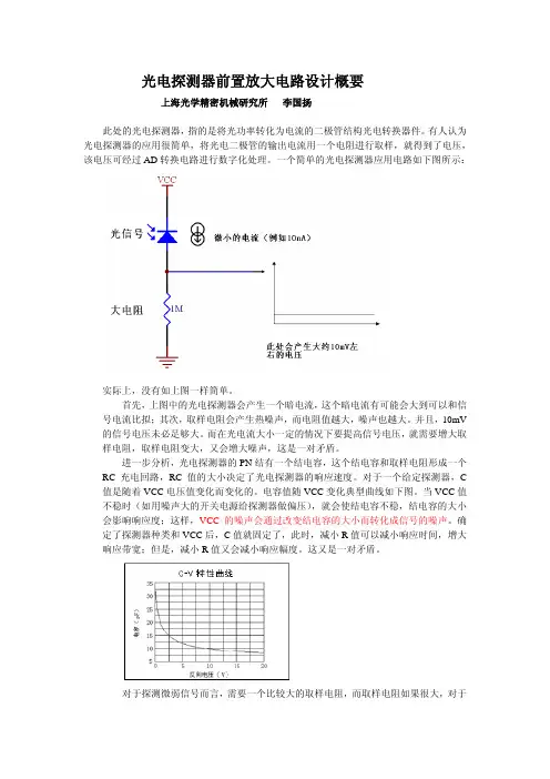
光电探测器前置放大电路设计概要上海光学精密机械研究所李国扬此处的光电探测器,指的是将光功率转化为电流的二极管结构光电转换器件。
有人认为光电探测器的应用很简单,将光电二极管的输出电流用一个电阻进行取样,就得到了电压,该电压可经过AD转换电路进行数字化处理。
一个简单的光电探测器应用电路如下图所示:实际上,没有如上图一样简单。
首先,上图中的光电探测器会产生一个暗电流,这个暗电流有可能会大到可以和信号电流比拟;其次,取样电阻会产生热噪声,而电阻值越大,噪声也越大。
并且,10mV 的信号电压未必足够大。
而在光电流大小一定的情况下要提高信号电压,就需要增大取样电阻,取样电阻变大,又会增大噪声,这是一对矛盾。
进一步分析,光电探测器的PN结有一个结电容,这个结电容和取样电阻形成一个RC充电回路,RC值的大小决定了光电探测器的响应速度。
对于一个给定探测器,C 值是随着VCC电压值变化而变化的。
电容值随VCC变化典型曲线如下图。
当VCC值不稳时(如用噪声大的开关电源给探测器做偏压),就会使结电容不稳,结电容的大小会影响响应度;这样,VCC的噪声会通过改变结电容的大小而转化成信号的噪声。
确定了探测器种类和VCC后,C值就固定了,此时,减小R值可以减小响应时间,增大响应带宽;但是,减小R值又会减小响应幅度。
这又是一对矛盾。
对于探测微弱信号而言,需要一个比较大的取样电阻,而取样电阻如果很大,对于后级电路来说,相当于一个大的输出阻抗,这对后级电路的处理带来了困难。
如下图所示意,如果后级电路的输入电阻为1M欧,那么信号电压只有一半被后级放大器提取,所以,要求后级电路有很大的输入阻抗,才能尽可能多的提取信号能量。
到了这里,您可能会说,是否可以选择一种光电探测器,使它能够对光信号更为敏感,也就是说,单位光功率可以得到更大一些的光电流,这样就减轻了电路的压力。
是的,有响应更大的器件。
但是,增大光电响应度,在半导体工艺上需要增大光敏面积,而增大光敏面积的一个伴生效应是增大结电容。