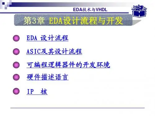
EDA设计流程及其工具
- 格式:ppt
- 大小:748.00 KB
- 文档页数:47
EDA技术与应用讲义第章第节EDA设计流程及其工具QUARTUSII快速设计指南-V1EDA技术与应用讲义是关于电子设计自动化技术(EDA)的一本权威教材,其中介绍了EDA设计流程及其工具QUARTUSII的快速设计指南。
本文将重点介绍第一章第节中关于EDA设计流程及其工具QUARTUSII的内容,并提供一些快速设计指南。
一、EDA设计流程EDA设计流程是EDA设计中不可缺少的重要步骤,它主要包括如下几个步骤:1.需求分析:需求分析是整个设计流程中非常关键的一步。
在这个阶段,设计师需要了解客户需求,制定出设计目标,明确设计范围,并且向客户提供关于设计方案的报告。
2.系统级设计:在系统级设计阶段中,设计师需要通过设计文档和模块图来描述整个系统的基本框架、模块间的通信方式和模块的功能特性等。
在这一阶段需要并且经常使用的工具包括:Microsoft Office、Mindmap、XMind等。
3.算法设计与仿真:在这个阶段,设计师通过各种仿真工具对系统进行算法的仿真和验证。
在这一过程中,设计师需要熟练掌握仿真和验证工具,比如MATLAB、Verilog等。
4.电路级设计:电路级设计是EDA设计流程的重要步骤。
设计师需要在此阶段使用EDA工具来实现电路的设计,并进行SPICE仿真。
常用的工具包括SPICE仿真器、电路设计与验证工具等。
5.物理设计:在物理设计阶段中,设计师需要对电路进行物理实现和布局。
可以使用EDA工具中的Autoplacer和Autorouter等工具。
二、QUARTUSII快速设计指南QUARTUSII是EDA设计中广泛使用的FPGA开发工具,它可以从高层次的RTL代码到底层的逻辑等级进行仿真和综合,最终生成bitstream文件上传到FPGA中实现电路的设计。
QUARTUSII的快速设计指南包括:1.了解quartus ii软件:在使用QUARTUSII之前,首先需要熟悉软件的基本操作和使用流程。
eda设计流程详解英文回答:EDA (Exploratory Data Analysis) is a crucial step in the data analysis process. It involves examining and visualizing the data to gain insights and identify patterns or relationships. EDA helps in understanding the data and making informed decisions before applying any statistical models or machine learning algorithms.The EDA process typically involves the following steps:1. Data collection: This step involves gathering the required data from various sources. It could be in the form of structured data from databases or unstructured data from text documents or web scraping.2. Data cleaning: In this step, the collected data is cleaned and preprocessed. This includes handling missing values, removing outliers, and transforming variables ifnecessary. Data cleaning ensures that the data is in a suitable format for analysis.3. Data visualization: Visualization is a powerful tool for understanding the data. It helps in identifying patterns, trends, and outliers. Various charts, graphs, and plots can be used to visualize the data, such as histograms, scatter plots, and box plots.For example, let's say I have collected data on the sales of a retail store. I can create a histogram to visualize the distribution of sales across different products. This can help me identify the most popular products and any potential outliers.4. Data exploration: This step involves exploring the data further by calculating summary statistics, such as mean, median, and standard deviation. It also includes identifying correlations between variables using techniques like correlation matrices or scatter plots.Continuing with the previous example, I can calculatethe average sales for each product category and compare them. This can help me identify any significant differences in sales between different categories.5. Hypothesis testing: In this step, statistical tests are performed to test hypotheses or assumptions about the data. This helps in making data-driven decisions and validating any patterns or relationships observed during the exploration phase.For instance, I can perform a t-test to determine if there is a significant difference in sales between two different time periods. This can help me understand if there has been any change in sales over time.6. Conclusion and insights: Finally, the EDA process concludes with summarizing the findings and drawing meaningful insights from the data. These insights can be used to guide further analysis or to make informed business decisions.中文回答:EDA(探索性数据分析)是数据分析过程中至关重要的一步。
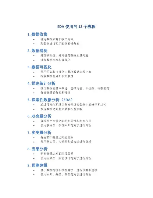
EDA使用的12个流程
1. 数据收集
•确定数据来源和收集方式
•对数据进行初步的探索性分析
2. 数据清洗
•处理缺失值、异常值等数据质量问题
•进行数据变换和规范化
3. 数据可视化
•使用图表和可视化工具将数据表现出来
•探索数据的分布和关联性
4. 描述统计分析
•统计数据的基本概述,包括均值、中位数、标准差等•分析变量的分布和特征
5. 探索性数据分析(EDA)
•通过可视化和统计分析来寻找数据中的规律和结构
•发现数据之间的关系和相互影响
6. 双变量分析
•分析两个变量之间的相关性和相互作用
•使用散点图、线性回归等方法进行分析
7. 多变量分析
•分析多个变量之间的关系
•使用热力图、多元回归等方法进行分析
8. 因果分析
•研究变量之间的因果关系
•使用因果图、实验设计等方法进行分析
9. 预测建模
•基于数据特征和模型算法,进行预测和建模
•使用回归、分类、聚类等方法进行分析
10. 模型评估
•对预测模型进行评估,包括准确率、召回率等指标
•使用交叉验证、ROC曲线等方法进行评估
11. 结果解释
•解释模型的结果和预测的意义
•提出结论和建议
12. 报告撰写
•将整个分析过程整理成报告
•包括数据分析的方法、结果和结论
以上是EDA使用的12个流程,通过这些流程可以帮助我们更好地理解和分析数据,发现其中的规律和关联性,并提供数据驱动的决策依据。
采用Markdown 格式进行编写可以使得文档结构清晰,便于阅读和理解。

立创eda电子设计流程介绍Electronic design automation (EDA) stands for a category of software tools for designing electronic systems such as printed circuit boards and integrated circuits.电子设计自动化(EDA)是指一类用于设计印刷电路板和集成电路等电子系统的软件工具。
它们可以帮助工程师快速、高效地完成设计工作,并在整个设计流程中提供支持。
The EDA process involves various stages, starting from design specification and requirements, through circuit design and simulation, to physical layout and fabrication.EDA过程涉及各个阶段,从设计规范和要求开始,通过电路设计和模拟,到物理布局和制造。
In the design specification and requirements phase, the engineer outlines the functionality and features of the electronic system. This phase sets the foundation for the entire design process and requires clear communication between the design team and the client.在设计规范和需求阶段,工程师概述了电子系统的功能和特性。
这个阶段为整个设计流程奠定了基础,并需要设计团队与客户之间的清晰沟通。
Following the design specification, the circuit design and simulation phase involves the creation and testing of the schematic diagram of the electronic system using specialized EDA software. This is a critical stage where the engineer simulates the behavior of the circuit to ensure it meets the desired functionality and performance.在设计规范之后,电路设计和模拟阶段涉及使用专门的EDA软件创建和测试电子系统的原理图。
EDA技术设计电路的设计流程EDA(Electronic Design Automation)技术是指通过计算机软件工具辅助进行电子电路设计、分析和验证的技术。
它可以提高设计师的效率和设计质量,并减少设计周期。
本文将详细描述使用EDA技术设计电路的设计流程,包括以下步骤:1. 需求分析在进行电路设计之前,首先需要明确电路的需求和要求。
这包括功能需求、性能指标、电源和环境条件等。
设计人员需要与客户或系统工程师进行充分的沟通和交流,确保对电路设计目标的共识。
2. 架构设计在需求分析的基础上,设计人员需要进行电路的架构设计。
在这一阶段,设计人员需要选择合适的电路拓扑结构、制定电路通信方式、确定信号处理算法等。
架构设计的目标是在满足需求的前提下,最大程度地降低功耗、电路面积和成本。
3. 电路原理图设计电路原理图是电路设计的基础,它描述了各个元件和电子器件之间的连接关系。
在EDA工具中,设计人员可以通过拖拽符号、连接引脚等方式来完成电路原理图的设计。
在这一阶段,设计人员需要根据架构设计的要求选择合适的元件,并进行连接。
此外,还需要进行信号的调节和滤波等处理。
4. 电路仿真电路仿真是验证电路设计的关键步骤之一。
通过仿真,设计人员可以预测电路的性能、稳定性和可靠性。
在EDA工具中,设计人员可以通过输入电路的参数和信号来进行仿真,并通过仿真结果进行分析。
常用的电路仿真工具有SPICE、Verilog等。
4.1 直流分析直流分析可以得到电路的稳态工作状态,包括电流、电压和功率等。
设计人员需要根据设计要求设置电路的直流电源和参数,并进行仿真分析。
4.2 交流分析交流分析可以得到电路在不同频率下的频率响应和滤波效果。
设计人员需要设置交流源和参数,并进行交流仿真分析。
4.3 时序分析时序分析可以得到电路在不同时钟频率下的时序性能,包括时钟延迟、数据到达时间和时序安全裕度等。
设计人员需要设置时钟源和时钟参数,并进行时序仿真分析。
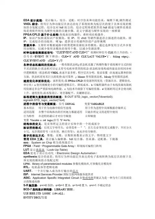
EDA设计流程:设计输入,综合,适配,时序仿真和功能仿真,编辑下载,硬件测试VHDL综合:将用行为和功能层次表达的电子系统转换为低层次的便于具体实现的模块组合装配过程,综合仅对hdl而言的,综合过程将把软件的hdl描述与硬件结果挂钩是将软件转化为硬件电路的关键步骤,是文字描述与硬件实现的一座桥梁FPGA/CPLD基于什么结构:查找表结构器件;乘积项结构器件。
IP:知识产权核或知识产权模块,软IP:用vhdl等硬件描述语言描述的功能块。
固IP:完成综合的功能块。
硬Ip:提供设计的最终阶段产品即掩模资源共享:主要针对数据通路中耗费逻辑资源较多的模块,通过选择复用方式共享使用该模块,以减少使用该模块的使用个数,以减少资源浪费。
时钟边缘检测描述语句:“CLK'EVENT AND CLK='1'” 检测时钟信号CLK的上升沿的,<信号名>'EVENT 侧下降沿:CLK=’0’AND CLK’LAST_V ALUE=’1’、falling_edge()、CLK’EVENT AND (CLK=’0’)等各种状态机编码的优缺点:一般有限状态机(\状态机克服了纯硬件数字系统顺序方式控制不灵活的缺点\状态机可以定义符号化枚举类型的状态\状态机容易构成性能良好的同步时序逻辑模块\状态机的VHDL表述丰富多样、程序层次分明,易读易懂\在高速运算和控制方面,状态机更有其巨大的优势\高可靠性 .)Moore型有限状态机.Mealy型有限状态机速度优化和面积优化:面积优化:指FPGA/CPLD的资源利用优化(资源共享,逻辑优化,串行化)a使用规模更小的可编程逻辑芯片,降低成本。
b可编程器件由于布线资源有限耗用资源过多会严重影响电路性能。
c为技术升级留下可编程资源。
d资源耗用过多会使功耗上升。
速度优化:流水线设计,寄存器配平,关键路径法。
标准逻辑矢量数据类型的赋值:B:OUT STD_logic_vector(7downto0);signalA:STD_logic_vector(1to4)进程中的信号与变量赋值:信号SIGNAL 变量V ARIABLE基本用法用于作为电路中的信号连线用于作为进程中局部数据存储单元适用范围在整个结构体内的任何地方都能适用只能在所定义的进程中使用行为特性在进程的最后才对信号赋值立即赋值变量Variable a: std_logic;信号Y<=a+b;结构体的定义:是实体所定义的设计实体中的一个组成部分标识符的格式:以英文字母开头,必须是单一“_”,且左右必须有英文或数字,不区分大小写,允许图形符号(回车符,换行符等),也允许有空格符。
eda设计流程详解英文回答:EDA (Exploratory Data Analysis) is a crucial step inthe data analysis process. It involves examining and analyzing data to gain insights, discover patterns, and identify outliers or missing values. In this answer, I will explain the EDA design process in detail.1. Data Collection: The first step in EDA is to collect the relevant data. This can be done through various sources such as surveys, experiments, or existing databases. For example, if I am analyzing customer satisfaction for a product, I might collect data through customer feedback surveys.2. Data Cleaning: Once the data is collected, it needsto be cleaned to ensure its quality and reliability. This involves removing any duplicates, correcting errors, handling missing values, and transforming data if necessary.For instance, if there are missing values in a dataset, I might choose to impute them with the mean or median values.3. Data Exploration: After cleaning the data, the next step is to explore it. This involves summarizing the data using descriptive statistics, visualizing the data through graphs or plots, and identifying any patterns or trends. For example, I might calculate the mean, median, and standard deviation of a numerical variable, and create a histogram or scatter plot to visualize the distribution.4. Feature Engineering: In this step, we create new features or modify existing ones to improve the performance of our models. This can include transforming variables, creating interaction terms, or encoding categorical variables. For instance, if I have a date variable, I might extract the day of the week or month as separate features.5. Statistical Analysis: EDA also involves conducting statistical tests to validate our findings or make inferences about the data. This can include hypothesis testing, correlation analysis, or regression analysis. Forexample, I might perform a t-test to compare the means of two groups or calculate the correlation coefficient between two variables.6. Outlier Detection: Identifying and handling outliers is an important part of EDA. Outliers can significantly impact our analysis and models, so it's crucial to detect and handle them appropriately. This can be done through various methods such as box plots, z-scores, or clustering algorithms. For instance, I might use a box plot toidentify any extreme values in a dataset.7. Data Visualization: Finally, EDA involves presenting our findings and insights through visualizations. This can include creating interactive dashboards, infographics, or reports. Visualizations help us communicate complex information in a more understandable and engaging way. For example, I might create a bar chart to compare the sales performance of different products.中文回答:EDA(探索性数据分析)是数据分析过程中至关重要的一步。
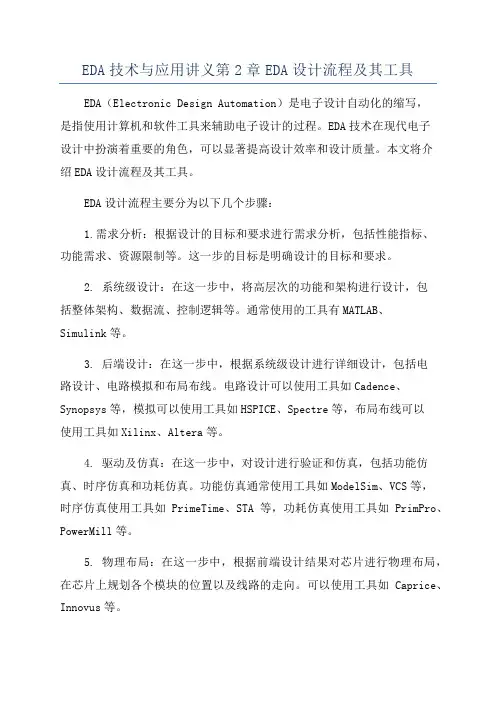
EDA技术与应用讲义第2章EDA设计流程及其工具EDA(Electronic Design Automation)是电子设计自动化的缩写,是指使用计算机和软件工具来辅助电子设计的过程。
EDA技术在现代电子设计中扮演着重要的角色,可以显著提高设计效率和设计质量。
本文将介绍EDA设计流程及其工具。
EDA设计流程主要分为以下几个步骤:1.需求分析:根据设计的目标和要求进行需求分析,包括性能指标、功能需求、资源限制等。
这一步的目标是明确设计的目标和要求。
2. 系统级设计:在这一步中,将高层次的功能和架构进行设计,包括整体架构、数据流、控制逻辑等。
通常使用的工具有MATLAB、Simulink等。
3. 后端设计:在这一步中,根据系统级设计进行详细设计,包括电路设计、电路模拟和布局布线。
电路设计可以使用工具如Cadence、Synopsys等,模拟可以使用工具如HSPICE、Spectre等,布局布线可以使用工具如Xilinx、Altera等。
4. 驱动及仿真:在这一步中,对设计进行验证和仿真,包括功能仿真、时序仿真和功耗仿真。
功能仿真通常使用工具如ModelSim、VCS等,时序仿真使用工具如PrimeTime、STA等,功耗仿真使用工具如PrimPro、PowerMill等。
5. 物理布局:在这一步中,根据前端设计结果对芯片进行物理布局,在芯片上规划各个模块的位置以及线路的走向。
可以使用工具如Caprice、Innovus等。
6. 物理布线:在这一步中,根据芯片的物理布局结果进行布线,将各个模块之间的连线完成。
主要使用工具有Innovus、Cadence等。
7. 物理验证:在这一步中,对芯片进行物理验证,包括DRC(Design Rule Checking)、LVS(Layout vs. Schematic)等。
可以使用工具如Calibre、Assura等。
8. 功能验证:在这一步中,对芯片进行功能验证,通过测试芯片的各种功能和逻辑是否与设计要求一致。

eda设计流程五个步骤英文回答:1. Problem Definition:The first step in the EDA (Exploratory Data Analysis) design process is to clearly define the problem. This involves understanding the objective of the analysis, identifying the data sources, and determining the scope of the project. It is important to clearly define the problem to ensure that the analysis is focused and relevant.2. Data Collection:Once the problem is defined, the next step is tocollect the relevant data. This may involve gathering data from various sources such as databases, APIs, or web scraping. It is important to ensure that the data collected is comprehensive and representative of the problem at hand. Data quality and accuracy are also important considerationsduring the data collection process.3. Data Cleaning and Preprocessing:After the data is collected, it needs to be cleaned and preprocessed to ensure its quality and usability. This step involves removing any duplicate or irrelevant data, handling missing values, and transforming the data into a suitable format for analysis. Data cleaning and preprocessing are crucial steps as they directly impact the accuracy and reliability of the analysis.4. Exploratory Data Analysis:Once the data is cleaned and preprocessed, the next step is to perform exploratory data analysis. This involves analyzing the data using various statistical techniques and visualizations to gain insights and understand the patterns and relationships within the data. Exploratory data analysis helps in identifying trends, outliers, and potential correlations between variables.5. Conclusion and Reporting:The final step in the EDA design process is to draw conclusions from the analysis and report the findings. This involves summarizing the key insights, presenting the results in a clear and concise manner, and making recommendations based on the analysis. The conclusions and reports generated from the EDA process can be used to inform decision-making and drive further analysis or actions.中文回答:1. 问题定义:EDA(探索性数据分析)设计流程的第一步是明确定义问题。
eda设计的基本流程-回复EDA(探索性数据分析)是数据科学中非常重要的一环,它旨在通过对数据进行初步的探索和分析,揭示数据背后隐藏的模式和趋势。
在本文中,我们将介绍EDA的基本流程,包括数据收集、数据预处理、数据可视化和模式发现等步骤。
第一步:数据收集数据收集是EDA的第一步,它涉及到查找和收集所需的数据集。
这些数据可以是来自各种来源,例如数据库、文本文件、实验室测量等。
在这一阶段,需要明确研究的目标和问提,以便确定需要收集的数据类型和格式。
第二步:数据预处理数据预处理是EDA的关键步骤之一,它旨在清洗和准备原始数据,以便后续的分析和可视化。
在这个过程中,需要处理缺失数据、异常值和重复数据等数据问题。
常用的数据预处理技术包括数据去重、填充缺失值、处理异常值和数据格式转换等。
第三步:数据可视化数据可视化是EDA的核心步骤之一,它通过图表和图形的形式将数据可视化展现出来,以便更好地理解数据的特征和关系。
通过数据可视化,可以发现数据中的趋势、模式和异常情况。
常用的数据可视化技术包括直方图、散点图、线图、饼图和热力图等。
第四步:模式发现和特征工程模式发现是EDA的核心目标之一,它旨在发现数据中的隐藏模式和有趣的关联。
通过模式发现,可以了解数据集中存在的潜在规律和趋势。
此外,特征工程也是EDA的重要部分,它涉及到对原始数据进行转换和提取,以便构建更好的特征集。
常见的模式发现技术包括聚类分析、关联规则挖掘和时间序列分析等。
第五步:数据分析和解释数据分析是EDA的最后一步,它旨在分析和解释数据背后的模式和趋势。
通过数据分析,可以对数据集中的关键问题进行定量的分析和评估。
此外,还可以利用统计分析和机器学习模型进行预测和分类。
在数据分析的过程中,需要根据具体的研究目标和问题选择合适的分析方法和工具。
综上所述,EDA的基本流程包括数据收集、数据预处理、数据可视化和模式发现等步骤。
通过系统地进行EDA,可以更好地理解和分析数据,从而为后续的数据建模和决策提供有力支持。
Altium Designer设计流程Altium Designer是一款功能强大且综合全面的电子设计自动化(EDA)软件,用于电子产品的原理图设计、PCB布局与布线、模拟仿真、多板设计以及输出制造文件等。
下面将详细描述Altium Designer设计流程的步骤和流程,以确保流程清晰且实用。
一、设计准备阶段在开始电路设计之前,需要进行一些准备工作,确保项目的顺利进行。
1.制定需求规格:明确设计目标,包括使用环境、功能要求、性能指标等。
例如,需要明确电路的工作电压范围、频率范围、输入输出接口等。
2.选择器件:根据需求规格,选择适合的IC和其他器件。
需考虑器件的性能、价格、供货情况等因素。
在Altium Designer中,可以使用库管理功能,将所选器件添加到库中。
3.创建项目:在Altium Designer中,点击File->New->Project,创建一个新的项目。
选择适合的项目类型(如Schematic、PCB)。
4.建立设计文件结构:在项目文件夹中,建立清晰的文件结构,用于存放原理图、PCB图、模型库、输出文件等。
5.建立原理图框图:创建原理图的标题、图例、尺寸线等标志,用于后续的原理图绘制。
二、原理图设计阶段原理图设计是电路设计的基础,通过连接各个器件的引脚,描述电路的结构和功能。
1.创建原理图:在导航栏中点击Project->Add New to Project,选择Schematic,创建一个新的原理图。
2.选择器件:使用库管理功能,从库中选择所需的器件。
可以通过名称、型号、关键词等进行搜索。
3.绘制电路图:在原理图上绘制电路图。
可以使用工具栏中的元件图形工具,在原理图画布上拖动元件并连接引脚。
为了提高绘制效率,可以使用键盘快捷键。
4.添加关键元件:在电路图中添加关键器件,如微处理器、存储器等。
需要注意连接方式、供电电源和信号线的细节。
5.添加文本和注释:在电路图中添加文本和注释,描述电路的功能和特点。
EDA开发流程开发流程在了解了硬件描述语言的演进过程中,相信各位对VHDL及Verilog HDL 与ASIC EDA工具之间的关系,应已有基本的认识。
在此,让我再强调一次:在高阶设计的领域中,硬件描述语言扮演的角色,只是一种程序语言接口(PLI);它提供了一个极具弹性的设计入口(design entry),以作为电路设计者与各种计算机辅助设计工具之间沟通的桥梁。
因此,若缺少了这些EDA工具,硬件描述语言的剩余价值,也只不过是一种系统规划工具,或是技术文件格式而已。
具体地说,整个数字电路的高阶设计概念,可以说就是设计自动化(design automatize)的实现。
理想的情况是:由仿真验证设计是否符合原始设定的规格(specification),以至于诸如逻辑电路的合成与实际晶体管配置与绕线(place and route)这一类徒手不易掌控的工作,工程师均能寻求适当的EDA 工具来完成整个电路的设计。
完整的自动化数字电路设计流程包含了三种主要的EDA工具:仿真器(simulator)、合成器(synthesizer)以及配置与绕线(place and routing, P&R)工具;除了P&R工具之外,其余两者绝大部分,均是以VHDL或Verilog HDL作为其程序语言接口。
以下,笔者将配合介绍这个典型的自动化设计流程,简述各项EDA工具的基本功用。
1.系统规格制定(Define Specification)在ASIC设计之初,工程师们须根据产品的应用场合,为ASIC设定一些诸如功能、操作速度、接口规格、环境温度及消耗功率等规格,以做为将来电路设计时的依据。
在这方面,目前已有厂商提供系统级仿真器(system -level simulator),为系统设计提供不错的解决方案;透过此类仿真器,工程师们可以预估系统的执行效能,并可以最佳化的考量,决定软件模块及硬件模块该如何划分。
电路设计中常见的EDA工具介绍电路设计是电子工程的重要分支之一,而电路的设计离不开EDA工具的支持。
EDA(Electronic Design Automation,电子设计自动化)工具是一些软件程序,可以辅助电路设计师完成从电路原理图到PCB(Printed Circuit Board,印刷电路板)布局的全过程。
本文将介绍电路设计中几种常见的EDA工具及其特点。
一、原理图绘制工具:EagleEagle是一款多功能的电子设计软件,用户可以使用它绘制电路原理图、设计PCB、布线等。
Eagle具有简单、易学、易用的特点,可以轻松应对小型电路的设计,而且其元器件库也非常丰富,几乎能够满足绝大部分的需求。
Eagle支持标准的Gerber输出格式,可以与各类CAM(Computer Aided Manufacturing,计算机辅助制造)软件无缝对接。
二、仿真工具:PSPICEPSPICE是由美国公司Cadence设计的一款电路仿真软件。
PSPICE是目前业内广泛使用的一款仿真工具,因其良好的仿真支持及完整的仿真模型而受到大量用户的青睐。
PSPICE能够对于线性、非线性、数字、模拟和混合信号电路进行精确的仿真分析,并提供充分的仿真结果分析与可视化手段。
此外,PSPICE还支持各类外部模型与设备的导入,可大大提升模型的准确性。
三、布局设计工具:Altium DesignerAltium Designer是一款基于Windows平台的PCB设计软件,经过多年的发展,它已成为市场上的佼佼者。
Altium Designer具有强大的元器件绘制和模块化设计引擎,可以支持多方面的设计工具。
其直观的用户界面、超快的地图绘制工具和高度自动化的功能导向使得用户通常可以极快地获得确定的结果。
同时,Altium Designer还可以与其他ECAD软件轻松集成,能够满足中等或大型的电路板设计的要求。
四、封装设计工具:PADSPADS是一个完全集成化的电子设计系统,提供了一个全面的、可靠的PCB设计问题解决方案。