Analysis and Simulation of a 1-18-GHz broadband double-ridged horn antenna
- 格式:pdf
- 大小:1.01 MB
- 文档页数:6

电子信息对抗技术Electronic Information Warfare Technology2020,35(4) 中图分类号:TN97 文献标志码:A 文章编号:1674-2230(2020)04-0088-04收稿日期:2019-09-26;修回日期:2019-10-16作者简介:赵利群,女,四川眉山人,工学硕士;胡助明,男,四川内江人,工学硕士㊂2~18GHz 宽带波束网络的设计赵利群1,胡助明2(1.成都西科微波通讯有限公司,成都610072;2.电子信息控制重点实验室,成都610036)摘要:给出了一种2~18GHz 宽带波束网络的设计方法,其核心电路由Wilkinson 功分器和平面巴伦构成,平面巴伦由开路和短路耦合传输线实现,最后基于ADS 完成了2~18GHz 宽带波束网络的仿真设计㊂仿真结果证明,该波束网络能够对来自四个不同天线的波束进行和差操作㊂关键词:Wilkinson 功分器;平面巴伦;和差波束DOI :10.3969/j.issn.1674-2230.2020.04.019The Design of 2~18GHz Broadband Beam -Forming NetworkZHAO Liqun 1,HU Zhuming 2(1.Chengdu Seekon Microwave Communication Co.Ltd,Chengdu 610072,China;2.Science and Technology on Electronic Information Control Laboratory,Chengdu 610036,China)Abstract :The design method of a broadband 2~18GHz beam-forming network is described.Wilkinson power divider and planar balun are core circuits of the broadband beam-forming net⁃work,open and short coupling transmission lines are composed of the planar balun.The design of the 2~18GHz beam-forming network is accomplished using ADS finally.Simulation results prove it can sum and difference beams coming from four different antennas.Key words :Wilkinson power divider;planar Balun;sum and difference beam-forming1 引言Wilkinson 功分器和Balun 都是成熟的宽带微波无源器件,将二者结合起来,实现了一种2~18GHz 宽带波束网络㊂它能对来自四个不同天线的波束进行和差操作㊂ADS 仿真结果证明,该波束网络能够工作在2~18GHz㊂值得一提的是,利用宽带开路/短路耦合传输线可以实现平面巴伦㊂2 设计过程2.1 设计方案该2~18GHz 宽带波束网络包括4个输入端口和3个输出端口,方案框图如图1所示㊂每个天线端接一分三Wilkinson 功分器,然后在进行和差操作:图1 2~18GHz 宽带波束网络方案框图88电子信息对抗技术·第35卷2020年7月第4期赵利群,胡助明2~18GHz宽带波束网络的设计和波束Σ=馈源1+馈源2+馈源3+馈源4;差波束Δ1=(馈源1+馈源3)-(馈源2+馈源4);差波束Δ2=(馈源1+馈源2)-(馈源3+馈源4);和”波束由Wilkinson功分器实现, 差”波束由Balun实现㊂根据图1所示,2~18GHz宽带波束网络共需要4个一分三功分器㊁7个一分二功分器以及2个平面巴伦㊂2.2 Wilkinson功分器的设计①一分二Wilkinson功分器的设计设计两路Wilkinson功分器可以根据SeymourB.Cohn提供的表格进行[1],为了进一步提高隔离度,选择N=9节两路带线Wilkinson功分器㊂基板为Rogers5880,厚度为1.574mm㊂每一节的阻抗和电阻经ADS优化之后得到,优化后的阻抗和电阻数据如表1所示,HFSS仿真模型如图2所示㊂HFSS仿真结果为:输入输出VSWR≤1.25,插损≤3.5dB,隔离度≥25dB㊂图2 一分二Wilkinson功分器HFSS仿真模型②一分三Wilkinson功分器的设计本文以牺牲1.77dB理论插损为代价,将一分四Wilkinson功分器的其中一路接50欧姆负载,变成一分三功分器来使用㊂其好处是:设计简便,且隔离度不会受影响㊂隔离度仿真结果如图3所示㊂现在观察图1,对4个一分三功分器而言,两个差波束和一个和波束是不一样的负载㊂ADS 仿真结果证明:若一分三功分器的隔离度较低(例如低于15dB),和波束插损曲线波动会异常增大㊂此处设计的一分三功分器牺牲了1.77dB的插损,但25dB的隔离度足以屏蔽负载不一致带来的不利影响㊂图3 一分三Wilkinson功分器隔离度的仿真结果2.3 宽带平面巴伦的设计①理论分析E.M.T Jones与J.T.Bolljahn等人详细分析过各种耦合传输线的奇/偶模阻抗和相位常数β(即波束k)[2]㊂现考虑耦合传输线部分端口开路或短路的情况,如图4所示㊂图4 耦合传输线开路和短路的ADS模型98赵利群,胡助明2~18GHz 宽带波束网络的设计投稿邮箱:dzxxdkjs@假设图4为无耗传输线(α=0),开路耦合传输线相位常数的双曲余弦函数为[2]:cos h (j β)=+Z oeZ oo+1Z oeZ oo-1㊃cos(θ)(1)短路耦合传输线相位常数的双曲余弦函数为[2]:cos h (j β)=+Z oeZ oo+1Z oeZ oo-1㊃cos(θ)(2)因此,图4所示的短路传输线的相位比开路传输线超前180°,理论上可以用它们来实现一个平面巴伦㊂②2~18GHz 开路与短路耦合传输线图4所示单节1/4波长开路/短路耦合传输线不能覆盖2~18GHz,需要采用多节1/4波长耦合传输线㊂通过级联9节1/4波长耦合传输线,能实现耦合度为-8.34dB 的2~18GHz 开路/短路耦合线㊂将两个-8.34dB 耦合线串接,可以实现一个耦合度为-3dB 的耦合传输线[3]㊂用ADS 完成了2~18GHz 开路耦合传输线与短路耦合传输线的仿真,仿真结果如图5和图6所示㊂图5 插损仿真结果图6 相位差仿真结果③宽带平面巴伦的设计若2~18GHz Wilkinson 功分器分别端接宽带开路与短路耦合传输线,即可实现2~18GHz 宽带平面巴伦,如图7所示㊂图7 宽带平面巴伦的原理图根据图7在ADS 里搭建了一个完整的宽带平面巴伦模型㊂ADS 仿真结果为:插损≤3.05dB,输入输出VSWR ≤1.15,隔离度≥27dB,相位差≤180°±0.5°,其中相位差如图8所示㊂图8 宽带平面巴伦相位差仿真结果综上所述,构成2~18GHz 宽带波束网络的核心电路 Wilkinson 功分器和平面巴伦已经完成设计,性能指标符合要求,可以进一步开展整个宽带波束网络的仿真㊂2.4 2~18GHz 宽带波束网络的设计根据图1所示的方案框图,笔者在ADS 中搭建了2~18GHz 宽带波束网络的完整仿真电路模型,如图9所示㊂图9 2~18GHz 宽带波束网络的ADS 模型9电子信息对抗技术㊃第35卷2020年7月第4期赵利群,胡助明2~18GHz 宽带波束网络的设计ADS 仿真结果分别如图10~14所示,所有仿真结果汇总在表2中㊂图10 输入输出VSWR的仿真结果图11 各端口插损的仿真结果图12 差波束Δ1输入时,各输出端口之间的相位差图13 差波束Δ2输入时,各输出端口之间的相位差图14 和波束Σ输入时,各输出端口之间的相位差表2 2~18GHz 宽带波束网络ADS 仿真结果汇总指标仿真结果输入输出VSWR ≤1.35隔离度≥30dB 插损≤12.2dBΣ输入的幅度一致性≤±0.1dB Σ端口输入的相位一致性≤±0.1°Δ1输入的幅度一致性≤±0.1dB Δ1输入的相位一致性≤±0.1°Δ2输入的幅度一致性≤±0.1dB Δ2端口输入的相位一致性≤±0.1°3摇结束语 利用Wilkinson 功分器和平面巴伦成功设计了一种2~18GHz 宽带波束网络㊂仿真结果表明,这种方法不仅实现了 和”与 差”功能,并且具有良好的VSWR㊁幅度一致性与隔离度,电性能指标优异㊂本文提到的设计数据均考虑了薄膜和微印电路的工艺能力以及微组装工艺的实现能力㊂因此,尽管只公布了2~18GHz 宽带波束网络的设计方法以及仿真结果,但仍不失为一种值得参考的设计思路㊂参考文献:[1] SEYMOUR B C.A Class of Broadband Three -PortTEM-Mode Hybrids[J].IEEE Transactions on Micro⁃wave Theory and Techniques,1968,16(2):110-116.[2] JONES E M T.Coupled-Strip-Transmission-Line Fil⁃ters and Directional Couplers[J].IRE Transactions on Microwave Theory and Techniques,1956(4):75-81.[3] CRISTAL E G.Theory and Tables of Optimum Symmet⁃rical TEM-Mode Couple-Transmission Line Direction⁃al Couplers[J].IEEE Transactions on Microwave The⁃ory and Techniques,1965,13(5):544-558.19。

2 GHz~18 GHz宽带有源巴伦芯片设计作者:杨楠杨旭达来源:《现代信息科技》2022年第06期摘要:对宽带有源巴伦电路结构进行了研究,基于0.13 μm GaAs pHEMT工艺,采用电磁仿真软件设计一款2 GHz~18 GHz单片集成宽带有源巴伦芯片。
经过流片加工及装配测试,有源巴伦芯片在2 GHz~18 GHz工作频段范围,输入到两输出端小信号增益分别为3.0 dB~3.5 dB、3.5 dB~4.7 dB,两输出端口幅度差≤1.2 dB,相位差180±5°以内,输出P1 dB功率值大于4 dBm,直流功耗约5 V/50 mA。
芯片尺寸为1.4 mm×1.9 mm×0.07 mm。
实测与仿真结果具有一定的一致性。
关键词:单片集成;有源巴伦;幅度差;相位差中图分类号:TN43 文献标识码:A文章编号:2096-4706(2022)06-0058-04Design of 2 GHz~18 GHz Broadband Active Balun ChipYANG Nan, YANG Xuda(The 13th Research Institute of China Electronics Technology Group Corporation,Shijiazhuang 050051, China)Abstract:This paper researches the broadband active balun circuit structure. Based on 0.13 μm GaAs pHEMT process, a 2 GHz~18 GHz monolithic integration broadband active balun chip is designed by adopting electromagnetic simulation software. After flow chip processing and assembly testing, the active baron chip operates in the frequency band range of 2 GHz~18 GHz, the small signal gain of the input to the two outputs is 3.0 dB~3.5 dB and 3.5 dB~4.7 dB respectively. The amplitude difference between the two output ports is less than or equal to 1.2 dB and phase difference is less than 180±5°. The output P1dB power value is greater than 4 dBm, and the DC power consumption is about 5 V/50 mA. The chip size is 1.4 mm×1.9 mm×0.07 mm. There is certain consistency between the measured and simulation result.Keywords: monolithic integration; active balun; amplitude difference; phase difference0 引言伴隨着当今社会信息化的快速发展,无线通信技术已经广泛应用在各个领域,如通信网络、定位系统、无线局域网、蓝牙等等,这些已经成为生活中不可或缺的部分。

飞机目标动态RCS仿真技术研究齐玉涛;张馨元;林刚;李建周【摘要】针对飞行器目标在实际飞行过程中由于飞行姿态变化对目标电磁散射截面(radar cross section,RCS)的影响,提出了一种新的动态目标电磁散射建模方法.首先,对飞行器目标精确建模问题,提出了利用激光扫描方法对真实目标进行外形扫描,再通过逆向重构技术得到目标精确几何外形;然后利用实际飞行过程中测试数据,将获取的目标相对于雷达视向角信息代入仿真程序中,使用一体化电磁散射计算软件对一定航路上运动目标进行仿真计算,消除飞行姿态扰动对仿真数据的影响,使动态目标电磁散射建模更加符合实际飞行情况.仿真结果表明,本文方法可快速、准确获取飞机目标动态RCS仿真结果,具有很好的工程应用价值.%In consideration of the influence of moving target to the target radar cross section (RCS), an exact RCS modeling method of moving target based on the measured data is proposed in this paper. Firstly, we use laser scanning method to build the precise geometric model of the real target. Secondly, we extract the parameters of the target motion characteristics in the actual flight and use the attitude angle in simulated program. Finally, we develop integration software to calculate the electromagnetic scattering, and eliminate the effect of attitude angle variation to make simulated results coincide with actual situation. The results show that it can obtain high accuracy results of aircraft dynamic RCS quickly, and have stronger applicability in engineering.【期刊名称】《电波科学学报》【年(卷),期】2019(034)001【总页数】7页(P97-103)【关键词】动态目标;逆向工程;雷达散射截面(RCS);电磁散射【作者】齐玉涛;张馨元;林刚;李建周【作者单位】中国飞行试验研究院, 西安, 710089;中国飞行试验研究院, 西安, 710089;中国飞行试验研究院, 西安, 710089;西北工业大学电子信息学院, 西安, 710072【正文语种】中文【中图分类】TN957引言目标电磁散射特性在隐身与反隐身技术中有着重要的研究价值,也是雷达信息系统的一个重要组成部分.其中目标的雷达散射截面(radar cross section,RCS)反映了目标对照射电磁波的散射能力,是表征目标特性最基本、最重要的参数[1].在实际情况中,目标总是处于运动状态,因此,对动态目标电磁散射特性研究具有非常高的实际价值.外场测量是获取动态目标电磁散射特性的主要手段,但外场测量试验需耗费大量的人力、物力及时间.因此,需对动态目标高精度电磁散射建模技术进行研究.目前,对于复杂目标静态电磁散射特性仿真已经做了大量研究,但对动态目标的仿真计算相对比较欠缺.文献[2]分析了气流对飞行姿态扰动的影响,基于准静态法分析了目标的RCS特性;文献[3-4]根据目标航迹解算了雷达视线角信息,并对姿态扰动采用了正态分布随机数进行修正,解算了目标动态RCS仿真值;文献[5]研究了静态数据获取动态特性过程中的坐标变换和姿态一致性问题.上述文献都是从理论上针对目标姿态变化对电磁散射特性影响进行分析,不能全面反映目标在运动状态下相对于测量雷达视向变化情况,且目标姿态扰动模型还需进一步验证[6];目标几何模型方面,现有研究普遍精度不足,进而影响仿真计算精确性,也不能对仿真算法的改进提供支撑.本文基于真实目标激光扫描数据和实际飞行测试数据,提出一种新的动态目标电磁散射建模方法.首先利用激光扫描方法获取目标外形扫描点云,采用逆向几何建模技术,获取目标高精度几何模型,然后利用实际飞行过程中测试数据,将获取的目标相对于雷达视向角信息代入仿真程序中,最后利用一体化的电磁散射计算软件进行仿真计算,从而获取典型运动状态下复杂目标电磁散射特征.本文研究成果既可对现有装备进行建模仿真,提高测试效率,也可对非合作目标进行电磁散射预估.1 复杂目标精确几何建模复杂目标精确几何模型是电磁散射建模的基础,以往研究过程中往往由于复杂目标几何模型不够精细,仿真计算结果不能准确反映目标散射特征.几何模型误差是电磁散射建模主要的误差源之一.为保证建模精确度,获取复杂目标精确三维模型,本文采用逆向重构技术对真实目标进行扫描建模.逆向工程技术[7]是进行产品开发、设计以及改进的重要技术手段,通常包括数据采集、数据处理和CAD(computer aided design)模型重建三个主要环节.数据采集是利用全站仪、手持式扫描仪、三维激光扫描仪等设备对真实目标表面进行扫描,测出目标表面的若干组点的几何坐标,为全面获取目标扫描数据,可多次对目标进行扫描.飞机目标点云数据采集采用激光三角法和激光束极坐标法两种方法进行测量,激光三角法对曲面曲率较大部位进行测量,激光束极坐标法对测量范围较大、曲面可测性好的曲面进行测量.图1为模型飞机机翼扫描点云.图1 某型飞机机翼扫描点云Fig.1 The point cloud data of aerofoil shape在逆向测量过程中,飞机目标采集的点云数据量一般都很大,而且不可避免地会引入噪音点,为提高建模效率,提升建模质量,需要对测量数据进行处理.对测量噪音点,采用高斯滤波算法、均值滤波算法或中值滤波算法,可有效去除测量毛刺.对测量数据采样处理,采用文献[7]中局部迭代插值方法进行处理,用较少的点云数据完整表达被测对象的特征信息.由于飞机目标点云数据量大,因此在建模前可对点云模型进行区域划分,然后利用三维建模软件(如CATIA、UG等)重构各区域外形曲面,最后将各部分曲面在三维建模软件中进行装配、合并,从而获取高精度飞机CAD模型.图2为获取的模型飞机三维几何模型.图2 某型飞机三维几何模型Fig.2 The 3D model of plane2 目标动态特征获取飞机目标动态测量主要采用地面测量雷达对目标进行跟踪测量,动态测量数据区别于静态数据,主要包括[8]:1) 目标运动时由于相对位置的实时变化而引入的姿态角变化.2) 在飞行过程中,由于气流或风力作用导致的飞机姿态扰动.这两个因素导致了飞机目标在飞行过程中姿态不断变化,对于复杂目标,由于散射机理复杂,微小的姿态扰动都会导致电磁散射特性产生较大变化,因此,需要对动态目标姿态精确计算.目标姿态角包含方位角和俯仰角二维信息.文献[3, 9]等是用飞机目标全空域静态RCS数据库,根据飞机性能参数和空气动力学原理生成航线,再通过插值生成航线上动态RCS序列.该方法一方面需要计算4π立体角内足够密集的目标RCS数据,仿真效率较低;另一方面,航线数据计算和引入的随机扰动模型不能精确描述真实目标运动特征.本文针对上述问题,通过真实试验测量数据确定飞机目标在典型飞行状态下测量雷达照射的姿态角信息,通过计算,得到一定航线上目标运动过程中的姿态角变化.由于是利用飞机和地面测量雷达实时记录的数据进行目标姿态角计算,测量误差对计算结果影响有限,能够比较准确地描述目标运动特征.对于非合作目标,可采用基于航迹及飞行动作对目标航向角、俯仰角和横滚角预估,结合测量雷达信息获取较高精度的目标运动特性.飞机姿态角常利用飞机上安装的惯性导航系统测量记录飞机的航向角、俯仰角和横滚角,然后利用雷达测量的方位角和高低角在同一时标下进行合成计算.若地面测量雷达在飞机机体坐标系中坐标为(xt(t),yt(t),zt(t)),可用式(1)和式(2)解算出雷达视线在目标坐标系中方位角φ(t)和俯仰角θ(t).雷达坐标系与目标坐标系关系如图3所示.有关坐标系变换关系,可参考文献[10]相关部分,本文不再赘述.(1)(2)图3 机体坐标与雷达坐标关系Fig.3 The relation of radar coordinate systems and plane coordinate systems3 一体化电磁散射计算对于飞机等大型复杂目标,由于目标尺寸大,散射机理复杂,在现有电磁散射计算方法中,若要满足计算精度要求,往往计算周期较长,而且对计算资源要求比较高,若采用物理光学法(physical optics,PO)等高频算法,现有计算软件往往忽略了边缘绕射及目标腔体散射,计算精度不足,而且缺乏一体化分析计算环境,这些都制约了电磁散射建模技术的工程应用.针对上述问题,本文以UG(Unigraphics)建模软件为开发平台,将研究开发的图形电磁计算(graphical electromagnetic computing, GRECO)方法、增量长度绕射系数(incremental length diffraction coefficients, ILDC)及弹跳射线(shootingand bouncing ray, SBR)法集成到UG软件中,形成一套集众多散射机理计算于一体的综合分析计算环境,具有计算速度快、精度高的特点,能够满足复杂目标电磁散射计算的需要.图4为本文计算用一个边长0.866 m,高1.5 m的三棱柱,入射波频率1 GHz,垂直极化.本文方法的具体实现算法可参考文献[11]和文献[12].图4(a)为三棱柱模型与文献结果,文献分别给出了PO、PO+MEC(等效电磁流)以及MoM(矩量法)计算结果.图4(b)为本文计算结果与电磁仿真商业软件FEKO计算结果的对比,FEKO设置为PO计算,从结果可看出,本文计算方法在偏离镜面反射区也可有较高精度.计算步进为0.5°,本文计算耗时为2分钟55秒,FEKO计算耗时3分钟23秒,从计算效率来说,本文计算方法也比较好.(a) 三棱柱及文献结果(a) Model of triangular prism and the results in the literature(b) 仿真结果对比(b) Comparison of simulation results图4 三棱柱及计算结果Fig.4 Triangular prism and simulation result目前很多被广泛使用的三维CAD软件(如CATIA、Pro/E等)都可以方便地导入到UG中去,因此高精度动态目标几何模型就可方便地使用一体化软件打开,并精确反映目标模型细节.利用UG提供的应用程序接口UG/Open 和UG/Open++,可将实际飞行过程中目标相对测量雷达姿态角信息在计算程序中进行设置,并根据其变化情况设置模型动态信息,就可对目标动态特性精确建模仿真.本文动态目标电磁散射建模技术研究流程图如图5所示.图5 动态目标电磁散射计算流程图Fig.5 The flow chart of moving target’s modeling4 计算结果对图2所示目标,选取飞机相对于地面测量雷达侧站平飞状态进行仿真计算.飞机飞行高度H=5 km,飞行速度260 m/s,航线投影与原点垂直距离8 km,测量雷达位置为坐标原点,模拟单脉冲测量雷达,仿真入射波频率为9.5 GHz,垂直极化.飞行航迹示意图如图6所示.图6 飞机飞行航迹示意图Fig.6 The diagram of airline依据飞机姿态信息与雷达测量角度,可得出飞机方位视向角和俯仰视向角,如图7所示.(a) 方位角(a) Angles of azimuth(b) 俯仰角(b) Angles of pitch图7 目标方位视向角和目标俯仰视向角Fig.7 Target’s angles o f azimuth and pitch目标飞行过程中RCS仿真结果如图8所示.图8 目标动态RCS仿真数据Fig.8 The simulation result of target’s RCS由于复杂目标RCS是姿态敏感的,姿态角的微小变化都会造成RCS的剧烈变化,本文仿例中,由于目标运动引起的观测视角变化,RCS动态范围达40 dB以上,RCS的动态特性比较符合实际测量情况.在计算效率方面,100个计算点,共耗时4分钟32秒,并且省去了网格剖分过程,实现了快速、高效计算.对图9所示F-35模型进行动态特性仿真,模型尺寸为13.4 m×10.7 m×3.5 m,模型按纯金属模型处理,入射波频率为10 GHz,VV极化.以真实飞机飞行过程中航线作为仿真数据来源,计算出目标方位视向角和俯仰视向角信息如图10所示,RCS仿真结果如图11所示.图9 F-35飞机三维模型Fig.9 Three-dimensional model of F-35 aircraft(a) 方位角(a) Angles of azimuth(b) 俯仰角(b) Angles of pitch图10 目标视向角度信息Fig.10 The angles of target图11 F-35飞机仿真数据Fig.11 The simulation result of F-35 aircraft5 结论本文提出了一种动态目标电磁散射建模的新方法.首先基于真实目标激光扫描点云数据和逆向重构技术获取目标高精度几何模型,再根据实际测试获取的目标姿态信息采用一体化电磁散射计算软件对目标动态RCS特性进行仿真,具有快速、高效的特点.本文研究方法是外场动态测量试验的重要补充,可为飞行试验航线设计和飞行方法制定提供重要参考,也可对非合作目标动态电磁散射特性进行预估,具有重要的实际工程应用价值.参考文献【相关文献】[1] 黄培康, 殷红成, 许小剑.雷达目标特性[M].北京:电子工业出版社,2005.HUANG P K, YIN H C, XU X J. Radar target characteristic[M]. Beijing:Publishing House of Electronics Industry,2005.[2] 苏东林, 曾国奇, 刘焱,等.运动目标RCS特性分析[J].北京航空航天大学学报,2006,32(12):1413-1417.SU D L,ZENG G Q,LIU Y,et al.RCS study of moving radar target[J].Joumal of Beijing University of Aeronautics and Astronautics, 2006, 32(12):1413-1417.(in Chinese)[3] 张晨新, 庄亚强, 张小宽,等.动目标雷达散射截面的建模研究[J].现代雷达,2014,16(12):66-69. ZHANG C X,ZHUANG Y Q,ZHANG X K,et al.A study modeling of moving target’s radar Cross Section[J].Modern radar, 2014,16(12):66-69.(in Chinese)[4] 刘万萌, 童创明, 王童,等.飞机运动特征对雷达检测性能的影响分析[J]. 空军工程大学学报(自然科学版),2017,21(1):7-12.LIU W M,TONG C M,WANG T,et al. Analysis of an influence of aircraft movement feature on radar detection performance[J].Jouranal of air force engineering university(natural science edition), 2017,21(1):7-12.(in Chinese)[5] 李金梁, 曾勇虎, 周波,等.飞机目标静态与动态测量姿态一致性[J]. 北京航空航天大学学报,2013,29(9):453-457.LI J L,ZENG Y H,ZHOU B,et al.Gestuer consistency of airplane target between static and dynamic measurement[J]. Joumal of Beijing University of Aeronautics and Astronautics, 2013,29(9):453-457.(in Chinese)[6] 刘佳, 方宁, 谢拥军,等.姿态扰动情况下的目标动态RCS分布特性[J].系统工程与电子技术,2015,37(4):775-781.LIU J,FANG N,XIE Y J,et al.Dynamic target RCS characterisitic analysis under the influence of attitude perturbation[J].Systems engineering and electronics,2015,37(4):775-781.(in Chinese)[7] 惠广裕, 冯巧宁, 吉宁.基于逆向工程的飞机曲面重建方法研究[J].计算机与数字工程,2015,43(6):1102-1106.HUI G Y,FENG Q N,JI N,et al.Reconstruction of aircraft surface based on reverse engineering[J].Computer & digital engineering,2015,43(6):1102-1106.(in Chinese)[8] 戴崇, 徐振海, 肖顺平.非合作目标动态RCS仿真方法[J].航空学报,2014,35(5):1374-1384. DAI C,XU Z H,XIAO S P.Simulation method of dynamic RCS for non-cooperativetargets[J].Acta aeronautica et astronautica sinica,2014,35(5):1374-1384.(in Chinese) [9] 庄亚强, 张晨新, 张小宽,等.典型隐身飞机动态RCS仿真及统计分析[J].微波学报,2014,30(5):17-21.ZHUANG Y Q, ZHANG C X,ZHANG X K,et al.Statistical analysis and simulation of typical stealth aircraft dynamic RCS[J]. Journal of microwaves, 2014,30(5):17-21.(in Chinese) [10] 周超, 张小宽, 吴国成.基于坐标转换目标动态RCS时间序列研究[J].火力与指挥控制,2014,39(3):56-59.ZHOU C, ZHANG X K,WU G C.Analysis on RCS time series of dynamic target based on coordinate transformation[J]. Fire control & command control, 2014,39(3):56-59.(in Chinese)[11] 李建周, 许家栋, 郭陈江,等.一体化雷达散射截面计算方法研究[J]. 西北工业大学学报,2003,21(4):449-452.LI J Z,XU J D,GUO C J,et al.Integeative RCS(radar cross section)calculation as a much more efficient method of RCS caulation[J].Journal of Northwestern Polytechnical University, 2003,21(4):449-452.(in Chinese)[12] 李建周, 吴昌英, 郑奎松,等.考虑多次散射的复杂目标一体化电磁散射计算[J].微波学报,2012(S2):6-10.LI J Z,WU C Y,ZHENG K S,et al. Integeative electromagnetic scattering calculation of complex targets with multiple scattering structures[J].Journal of microwaves, 2012(S2):6-10.(in Chinese)。

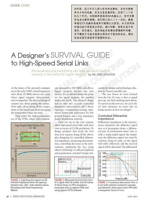
ferential impedance from the spacing between two .005” wide stripline traces. Simulated with Polar InstrumentsSI8000.of a signal after 26 inches and 40 inchesof travel down an FR-4 backplane,measured with an Agilent VNA andusing Agilent PLTS software.FIGURE 3.Conductor attenuation from a5 mil wide stripline conductor (orange)and dielectric attenuation from FR4 witha dissipation factor of 0.02.impedance of all the traces in the board must be at the target value, typically 100 Ω, in order to assure acceptable received signal amplitude and rise time.This is primarily achieved by the selection of line widths, spacing, dielec-tric thickness and knowing the dielectric constant of the laminate materials. The only way of accurately balancing the board stackup and evaluating the toler-ance buildup is with a 2D field solver .FIGURE 1explores how the spacing between two stripline traces affects their differential impedance. An easy-to-use,accurate 2D field solver is an essential tool to survive in this new regime.It is not the losses in the intercon-nects that cause problems in high-speed serial links – it is the frequency depend-ency of the losses. Both conductor loss and dielectric loss absorb more of the higher-frequency components than of the low-frequency components. This means that if you launch an ideal square wave into an interconnect, the rise time will degrade and get longer as it propa-gates, because the higher frequencies that make up the sharp edge are removed. This is illustrated in FIGURE 2.This rise time degradation causes most of the significant problems with high-speed serial interconnects, such as intersymbol interference (ISI), deter-ministic jitter and collapse of the eye diagram. It can be most easily described as the attenuation or loss in the signal as a function of frequency.Conductor loss is frequency-dependent due to skin depth effects.The cross-sectional area for current to travel through a conductor decreases into a thinner and thinner perimeter shell as frequency goes up. This increases the series resistance of boththe signal and return conductors at higher frequency.The only way to reduce the losses from the conductors’ series resistance is by using wider lines. But to use wider lines while still maintaining the target impedance also requires either thicker dielectric layers or lower dielectric constant.Of course, there is a limit to the total thickness of a board. With as many as 40 layers, in .250˝total thickness, the maximum dielectric thickness is on the order of .006˝already. And thicker boards will be more expensive due to material and drilling costs. Further , as we shall see, a thicker board also means longer via stubs, which will cause addi-tional signal integrity problems.Balancing the widest line for lowest rise time degradation, thinnest total board and acceptable cost can only be done with a simulation tool that includes lossy line effects, such as Men-tor Graphics HyperLynx or Agilent Technologies ADS.The second source of frequency-dependent loss comes from the dissipa-tion factor of the laminate. This mate-rial property is a measure of the dipoles in the laminate, which can rotate in the applied field of the signal and suck out energy from the signal.The higher signal frequency compo-nents will rotate the dipoles faster and cause more heat generation. Even though the dissipation factor of most materials is constant with frequency,the attenuation from the dissipation factor will increase with higher fre-quency. A low dissipation factor will minimize the rise time degradation.Insertion loss is a common metric to quantify the frequency-dependentloss of a signal as it propagates down an interconnect. This can be further refined as the attenuation in dB per inch of interconnect. A larger and more negative dissipation factor will mean less high-frequency signal and longer rise time, a bad thing. FIGURE 3shows an example of the insertion loss for both conductor loss and dielectric loss.As a rough rule of thumb, with many popular SERDES chips the typical acceptable attenuation might be as high as -10 dB at the bandwidth of the high-speed serial link, which is about half the bit rate. For a XAUI interface, at 3.125Gbps the bandwidth is about 1.6 GHz.If the interconnect length were 40 inch-es, the acceptable attenuation per length would be about -10 dB/40 inches, or ~ -0.25 dB/inch, at 1.6 GHz.In the example above, the total attenuation from the conductor loss and dielectric loss would be -0.12 dB/inch +-0.15 dB/inch = -0.27 dB/inch. This is above the estimated acceptable limit,which suggests a marginal design.For a robust design, either the line width must be increased, the dissipa-tion factor decreased, the interconnect length decreased, the SERDES noise margin increased, or silicon processing (i.e., pre-emphasis in the drivers)would have to be used.The Power of Pre-emphasisThe problem with attenuation in inter-connects isn’t the attenuation – it’s the frequency dependence that causes rise time degradation. If we know how much the higher frequencies will be attenuated and put an extra amount of these into the signal when it is launched, we might be able to see asharper rise time at the receiver. TheFIGURE unched signal with pre-emphasis from an Altera Stratix GX FPGA. (Figures 4, 5 and 6 courtesy ofAltera Corp.)FIGURE 5. Eye diagram of a XAUI sig-nal received after 57 inches in an FR-4backplane trace.The signal is unusable.FIGURE 6. The same FR-4 interconnect,57 inches in length, as in Figure 3, but with pre-emphasis used in the driver,utilizing the Altera Stratix GX FPGA.technique of adding high-frequency components into the launched signal is called pre-emphasis.An example of the time domain waveform of the launched signal with pre-emphasis is shown in FIGURE 4.There is an extra pulse at the tran-sitions. When this signal travels down the interconnect, the extra high-fre-quency components will be absorbed, flattening the waveform back into a more normal looking waveform. Pre-emphasis is a powerful technique of recovering a signal at the far end of a lossy line.In FIGURE 5is displayed the eye diagram of a XAUI signal, received after 57 inches in an FR-4 intercon-nect. There is so much frequency-dependent attenuation that all the bits are grossly distorted and cannot be read with any certainty. This intercon-nect is completely unusable.However, with pre-emphasis, extra high-frequency components are added to the signal and the frequency-dependent attenuation sucks out these extra components, leaving behind a much more usable signal. This is shown in FIGURE 6.The combination of conventional FR-4 boards and pre-emphasis in the drivers is a powerful combination for designing successful high-speed serial links. The higher the bandwidth, the greater the need for wider lines, lower dissipation factor and silicon processing.Though pre-emphasis can over-come losses in the interconnect, it can-not overcome the sharp resonances from via stubs. Ultimately, these stubs will be a fundamental limit to the bit rate for backplane interconnects.If conductor and dielectric loss were the only processes decreasing the insertion loss with frequency, pre-emphasis could compensate. Unfortu-nately, the stubs created by through vias can act as resonators and absorb a very large amount of the signal energy in narrow frequency bands. An exam-ple of the measured insertion loss of a backplane channel with and without a via stub is shown in FIGURE 7.The resonator is created when a signal uses a through via to transition from two closely spaced layers, such as between layers 1 and 4 or 2 and 5 in aBackdrilled via200-mil through-hole via stub0-20-40-60-80-10005101520Even lower frequency bit rates can suffer from via stub resonances, if their bandwidths are riding on the edge of the resonance curve. The most effective way of eliminating this problem is to move the via stub resonant frequency as high as possible, by using as short a via stub as possible. This can be done by removing NFPs from unused layers, limiting layer transitions to those near the outer layers, and backdrilling any stubs that might be left.Backdrilling is the process of re-drilling the bottom of the via with an oversized drill bit, after the through via has been plated. This removed the plat-ed through hole that is not being used and eliminates the resonating stub. FIG-URE 8shows an example of an as-fab-ricated through-hole via in an 18-layer board, and a similar via that has been backdrilled to remove the long stub.Backdrilling has become the de facto standard in all high-performance backplanes used in systems at 5 Gbps and above. To allow scalability of a backplane that may be first used at 2.5 Gbps or even 3.125 Gbps, so that it could be used later in life at 5 Gbps, backdrilling is often employed. This way, higher bit rate cards can be plugged into this legacy backplane and still operate acceptably.Beginning of an EraIn this new era of high-speed serial links operating at 2 Gbps and above, a new set of signal integrity concerns must be considered for a system to work the first time. In addition to all the other signal integrity problems like terminations and topologies, crosstalk, ground bounce and power distribu-tion, now we must design out differen-tial impedance problems, deal with losses and include via stub effects.To survive this new set of mine-fields requires new skills, new tools and new technologies. The elements of survival include the use of 2D field solvers to accurately design the stackup and routing for differential pairs, the selection of optimal dielectric materials with low dielectric constant to allow wide lines and thin boards, low dissi-pation factor for low insertion loss and the use of silicon processing such as pre-emphasis. Finally, techniques to minimize the length of via stubs suchas backdrilling are essential.Now interconnects are not onlynot transparent but are the dominantfactor determining whether a large,high-performance system will work thefirst time, every time. By paying carefulattention to all of these importantissues, you can be successful in this eraand earn the right to face the chal-lenges of the next generation of high-performance systems. PCD&MERIC BOGATIN is the CTO at IDI, andpresident of Bogatin Enterprises. He canbe reached at eric@.REFERENCES1.This paper is based on Online Lecture 184,A Designer’s Survival Guide to High-SpeedSerial Links, posted on www.bethe. To view this lecture for free,enter coupon code PCDM0507.2.Bogatin, Eric, Signal Integrity - Simplified,Prentice Hall, 2003.。
Effect of Fe-coating on electromagnetic performance of hollow carbon fibers Xie Wei1, a, Cheng Hai-Feng2,b, Kuang Jia-cai3, a,Chu Zeng-Yong2,b, LongChun-guang1,a1School of Automobile and Mechanic Engineering, Changsha University of Science and Technology,Changsha, 410114,China2Key Lab of Advanced Ceramic Fibers & Composites, National University of Defense Technology,Changsha 410073, China3Institute of Materials Science and Engineering, Changsha University of Science and Technology,Changsha 410114,Chinaa email:**************, b**************.cnKeywords: carbon fibers; electromagnetic performance; coatingAbstract: Hollow carbon fibers were coated with Fe by chemical deposition to improve their electromagnetic performance. A parallel experiment was designed to investigate their chemical reactivity and surface curvature. The microstructure, composition, phase analysis and electromagnetic performance of Fe-coated and uncoated hollow carbon fibers were studied using SEM, EDAX, XRD and voter network analysis. The result indicates that magnetic loss is introduced due to the inherent property of iron. The real and imaginary parts of the complex permeability (μ′ and μ″) of the composites, which consist of the paraffin and the coated fibers after pretreatment and surface activity, are 1.44 and 0.54 at 2 GHz, respectively.IntroductionIn recent years, microwave absorbing materials have attracted considerable attention because they are an essential part of stealthy defense system for all military platforms, whether as aircraft, sea or land vehicles. They are also used to eliminate electromagnetic interference (EMI), which is a specific kind of environmental pollution due to the explosive growth in the utilization of electrical and electronic devices in industrial and commercial applications. To date, the needs for microwave absorbing materials with a combination of high mechanical properties, good heat resistant and excellent stealth are becoming more and more urgent [1-3]. Hollow carbon fibers (HCFs), with dual-layer structure, have been considered to be a promising candidate in the microwave absorbing materials field [4-6]. In principle, the electromagnetic performance of a single-layer microwave absorbing material can be improved by adjusting the complex permittivity and permeability of absorbers. Therefore, it is necessary to deposit magnetic coatings onto HCFs, particularly of iron, nickel and cobalt or their alloy [7-8]. In addition, many efforts have been devoted into the preparation of carbon fibers and carbon nanotubes with metallic coating by electroless deposition because of their potential applications such as nanoscale electronic device [9-11]. For example, Xie et al. [12] prepared continuous and uniform Ni-Fe-Co-P coatings onto coiled carbon nanofibers via electroless deposition. The coated carbon nanofibers exhibit fine electromagnetic wave absorbing property in the frequency region of 8-18 GHz.Based on the similarity of carbon fibers and HCFs, a novel Fe-coated HCF has been fabricated by chemical deposition in this work. The characterization and electromagnetic performance of HCFs and Fe-coated HCFs were investigated in detail.Experimental procedureFig.1 shows the flow chart of preparation HCFs and Fe-coated HCFs. PAN hollow fibers used as the starting materials were spun by a dry-wet spinning setup described elsewhere [13]. The oxidation and carbonization condition of PAN hollow fibers refered to [14-16]. The parallel experiment was designed to investigate their specific structure in comparison with general carbon fibers. The preparation of Fe-coated HCFs was characterized as follows:(1) the HCFs were suspended in anhydrous ethanol and the mixture of butanol and xylene, and kept in a ultrasonic field for 30 minutes, then were subjected to an oxidation treatment in the nitric acid to modify the surface chemistry activity and improve dispersion, and washed with distilled water and ethanol subsequently, (2) thetreated HCFs and Fe(CO)5 were then introduced into the reactor of pyrolysis of carbonyl, which contained 5mL Tween-20 as a surfactant, and isolated from the air. High purity nitrogen gas (99.999%) was introduced into the system with a flow rate of 150 mL/min to prevent the oxidation of iron. The reaction carried out in an oil bath of 220°C for 60 minutes. The Fe(CO)5 vapor decomposition takes place showing in Eq.(1) [17-18].The chemsorption of iron on the surfaces of HCFs is achieved by joining iron to the self-assembled monolayers.Δ5(CO)5CO Q Fe Fe ⎯⎯→+↑− (1)The surface morphologies of HCFs and Fe-coated HCFs were characterized by scanning electron microscope (SEM) using JSM-6700F microscope. The elemental composition of HCFs and Fe-coated fiber was studied by energy dispersive X-ray spectrometry (EDAX), which the microprobe was associated with SEM. The phase analysis of fibers was performed by X-ray diffraction (XRD) on a D8ADVANCE type, using CuK α radiation with 2θ from 20° to 50°. The microwave magnetic properties of the Fe-coated HCFs were expressed by the complex permeability of the Fe-coating, and the Transmission/Reflection(T/R) coaxial line was used to determine the electromagnetic parameters of the HCFs. The measurement setup consisted of an Agilent 8720ET vector network analyzer with a synthesized sweep oscillator source and an S-parameter test set. A gold-plated coaxial air line with a precision 7 mm connector interface was used to hold the samples. The relative complex permeability μ=μ'-j μ″(μ′-the real part of the complex permeability, μ″-the imaginary part of the complex permeability) and relative complex permittivity ε=ε'-j ε″(ε′-the real part of the complex permittivity, ε″-the imaginary part of the complex permittivity) of the samples were calculated from the measuredFig.1. The experimental flow chart of HCFs and Fe-coated HCFs Results and discussionSEM micrographs of the original HCFs and Fe-coated HCFs are shown in Fig.2. Fig.2(a) shows a typical morphology of the uncoated HCF whose outer diameter is about 120μm and inner diameter is about 70μm. The HCF has an asymmetric structure with a lot of irregular micropores. Its structure differs from that of general carbon fiber. Fig.2 (b) and (c) show the Fe-coated HCFs without and with proper pretreatment and surfactant, respectively. We can see that the Fe-coating of HCFs after pretreatment and surface activity is continuous and uniform. The cross-section of the fiber without proper pretreatment and surfactant seems smooth and the micropores are not covered, while the micropores of the coated fiber after pretreatment and surface activity are covered by Fe conglomeration. The deposited iron is formed as spherical grains, which appear to be very closely to packed crystallites. It is noticed that the deposited layer is sensitive to the proper pretreatment and Tween-20, which subsequently influences the chemical reactivity and curvature of the fiber. Parallel results also show that the fabricated HCFs have low chemical reactivity and large surface curvature, therefore it is difficult to produce a continuous coating for HCFs without proper pretreatment and surfactant.Fig.2. SEM micrographs of the fiber, in which (a), (b) and (c) are referring to the samples in Fig.1respectively. 0123456789102004006008001000(a)C, O, Ca R e l a t i v e i n t e n s i t y (C o u n t s )Energy(keV) 01234567891020040060080010001200(b)Fe C, O, Ca R e l a t i v e i n t e n s i t y (C o u n t s )Energy(keV) 012345678910100200300400500600700800C, O, CaCa Fe Fe (c)R e l a t i v e i n t e n s i t y (C o u n t s )Energy(keV)Fig.3. Surface morphologies and EDAX patterns of the selected area of the fibersTable1 The weight and atom percent of elemental composition of the surface of the HCFs andFe-coated HCFsWt% At%samplesC O Ca Fe C O Ca Fe (a) 96.86 2.840.30 97.76 2.150.09(b) 90.85 8.790.130.2493.14 6.760.040.05(c) 7.23 0.59 1.4290.7726.17 1.60 1.5470.68The EDAX data of fiber in Fig.3 and Table 1 reveals that the surface of the coated fibers without proper pretreatment and surfactant is not continuous. The presence of calcium stems from the measurement system and oxygen relies heavily on the oxidation and carbonization condition of PAN hollow fibers. The absence of carbon and oxygen of the coated HCF after proper pretreatment and surfactant is a result of continuous and uniform Fe-coating.Showing in Fig.4, the X-ray spectra of uncoated and coated fibers exhibits that the coated fiber consists of a carbon phase as the majority phase and a small amount of α-Fe phase. There is no sign of Fe phase before surface treatment, while it appears after surface treatment although the intensity is relatively low. Combined with the analysis of SEM, EDAX and XRD, it is clearly confirmed thatFe-coating has been coated onto HCFs.Fig.4. XRD patterns of (a), (b) and (c)Fig.5 shows the ε′, ε″, μ′ and μ″ of the uncoated and coated fibers/paraffin composites in the frequency range of 2-18 GHz. The uncoated HCF is a typical conductive absorber. At 2 GHz, the μ′ and μ″ of the coated fibers after pretreatment and surface activity/paraffin composites are 1.44 and 0.54, and the μ′ and μ″ of the coated fibers without proper pretreatment and surfactant /paraffin composites are 1.23 and -0.10, respectively. It can be seen that the electromagnetic parameters of the HCFs relatively increase with Fe content increasing. The effect of Fe-coating on the electromagnetic performance of the HCFs /paraffin composites may be that magnetic loss is introduced due to the inherent property of iron. These electromagnetic properties, resulted from the increase of magnetic loss and conductive loss in this frequency region, can be applied to the microwave absorbingFig.5. Electromagnetic parameters of samples vs microwave frequency The results also indicate that Tween-20 plays an important role in the thickness of Fe-coating, which the thickness influences on the electromagnetic performance due to the intensity of the introduced magnetic loss. The original HCFs with proper pretreatment and surfactant can increase the coating thickness. So proper pretreatment and surfactant are necessary.ConclusionsIn conclusion, HCFs with Fe-coating have been prepared by chemical deposition. The surface pretreatment of HCFs is an important step before deposition. Tween-20 plays an important role in the thickness of Fe-coating. Magnetic loss is introduced due to the inherent property of the iron. Fe-coated HCFs can regulate the electromagnetic parameters of composites, which improves the microwave absorbing ability of general absorber. The Fe-coated HCFs may be useful for microwave absorbing materials.AcknowledgementThe financial support of the Nature Science Foundation of Hunan(08JJ3100), the Planned Science and Technology Project of Hunan Province(2010FJ4094) and Changsha University of Science and Technology are gratefully acknowledged.References[1]Petrov V M, Gagulin V V. Microwave Absorbing Materials. J Inorg Mater 2001; 37(2):93-98.[2]Woo S C, Dai G L. Development of the composite RAS (radar absorbing structure) for theX-band frequency range. Compos Struct 2007; 77: 457-465.[3]Zhao N Q, Zou T C, Shi C S, Li J J, Guo W K. Microwave absorbing properties of activatedcarbon-fiber felt screens(vertical-arranged carbon fibers)/epoxy resin composites. Mat Sci Eng B 2006;127:207-211.[4]Tsai H A, Ciou Y S, Hu C C, Lee K R, Yu D G, Lai J Y. Heat-treatment effect on the morphologyand pervaporation performances of asymmetric PAN hollow fiber membranes. J Membrane Sci 2005;255:33-47.[5]Lan Y J, Tai S C, Raj R. Dual-layer hollow carbon fiber membranes for gas separation consistingof carbon and mixed matrix layers. Carbon 2007; 45 166-172.[6]Park S J, Seo M K, Shim H B. Effect of fiber shapes on physical characteristics of non-circularcarbon fibers-reinforced composites. Mat Sci Eng A 2003; 352:34-39.[7]Yi Y, Zhang B S, Xu W D, Shi Y B, Jiang Z S,Zhou N S etal.Preparation and properties of anovel iron-coated carbon fiber. J Magn Magn Mater 2003;256:129-132.[8]Pan X F, Mu G H, Shen H G, Gu M Y. Preparation and microwave absorption properties ofelectroless Co-Ni-P coated strontium ferrite powder. Appl Surf Sci 2007; 253:4119-4122. [9]Xu J, Yang H B, Fu W Y, Sui Y M,Zhu H Y, Li M H, etal. Preparation and characterization ofcarbon fibers coated by Fe3O4 nanoparticles. Mat Sci Eng B 2006;132:307-310.[10]S hen X, Gong R Z, Nie Y, Nie J H. Preparation and electromagnetic performance of coating ofmultiwall carbon nanotubes with iron nanogranule. J Magn Magn Mater 2005; 288:397-402. [11]C he R C, Peng L M, Duan X F, Chen Q, Liang X L. Microwave absorption Enhancement andComplex permittivity and Permeability of Fe Encapsulated within Carbon Nanotubes. Adv Mater 2004;16(5):401-405.[12]X ie G W, Wang Z B, Cui Z L, Shi Y L. Ni-Fe-Co-P coatings on coiled carbon nanofibers. Carbon2005; 43:3181-3194.[13]Y ang M C, Chou M T. Effect of post-drawing on the mechanical and mass transfer properties ofpolyacrylonitrile hollow fiber membranes. J Membrane Sci 1996; 116:279-291.[14]S tephen D, Frank H, Peter M B.Thermal stabilization of polyacrylonitrile fibres. Polymer1999;40: 5531-5543.[15]E lisa B C, Vera M S, Cristiano P B. Preparation of carbon hollow fiber membranes by pyrolysisof polyetherimide. Carbon 2003; 41: 1707-1714.[16]S un J F. Study on the structure and properties of Polyacrylonitrile-based activated hollow carbonfiber. Donghua Univ. PhD thesis, 2004.[17]L ee G H, Huh S H, Park J W, Ri H C, Jeong J W. Arrays of Ferromagnetic Iron and CobaltNanocluster Wires. J Phys Chem B 2002; 106(9):2123-2126.[18]N ie Y, He H H, Zhao Z S, Gong R Z, Yu H B. Preparation, surface modification and microwavecharacterization of magnetic iron fibers. J Magn Magn Mater 2006; 306(1):125-129.[19]A bdulnour J, Akyel C, Wu K. A generic approach for permittivity measurement of dielectricmaterials using a discontinuity in a rectangular waveguide or a microstrip line. IEEE Trans Microwave Theory Tech 1995; 43(5):1060-1066.[20]V anzura E J, Baker-Jarvis J R, Grosvenor J H, Janezic M D. Intercomparision of permittivitymeasurements using the transmission/reflection method in 7-mm coaxial transmission lines.IEEE Trans Microwave Theory Tech 1994; 42 (11): 2063-2070.。
硅基马赫曾德电光调制设计优化与实现周林杰;周砚扬;陆梁军【摘要】In this paper,the design optimization and experimental demonstration of single-drive push-pull silicon electro-optic modulators are presented. In order to improve the modulation efficiency and lower the optical propagation loss,the PN junction profile and doping concentrations are firstly optimized. Next,the impedance match,phase match and microwave loss are studied,and in particular,the influence of low-doping slab width,travelling-wave electrode (TWE) width and spacing on the modulator performance are analyzed. Following the comprehensive theoretical analysis and numerical simulation,the modulator performance measurements,including the optical transmission spectrum upon single-drive push-pull tuning,small-signal microwave signal response,and high-speed digital signal modulation are consequently carried out. The on-chip insertion loss of the modulators is around 7-9 dB and the half-wave voltage is 5 V. At a bias voltage of 0 V,the optimized modulator has a modulation bandwidth of >18 GHz. The microwave reflectivity at the entrance of the TWE is less than -20 dB,suggesting good impedance match. When the reverse bias voltage is increased to 4 V,the modulation bandwidth can exceed 30 GHz,allowing for realization of 56 Gbit/s on-off keying (OOK) and 40 Gbit/s binary phase-shift keying (BPSK) modulations.%对单端推挽驱动硅基调制器进行了优化设计和实验验证.为了获得较高的调制器性能,首先对PN结的结构参数和掺杂浓度进行了仿真优化,以提高调制效率并降低光传输损耗;其次,对行波电极的阻抗匹配、相位匹配和微波损耗予以了研究,重点分析了低掺杂平板区宽度、行波电极传输线宽度(TWE)和间距对调制性能的影响.在理论分析和仿真计算的基础上,对单端推挽驱动调制器进行了频谱测试、小信号响应测试和高速调制码型测试.调制器的片上插入损耗在7~9 dB,半波电压约为5 V.偏置电压为0 V时,优化后的调制器的带宽大于18 GHz,入射端反射系数低于-20 dB,行波电极具有较好的阻抗匹配.当反偏电压大于4 V时,调制器的带宽可增加到30 GHz以上,并且能实现56 Gbit/s的二进制强度(OOK)调制和40 Gbit/s的二进制相移键控(BPSK)调制.【期刊名称】《中兴通讯技术》【年(卷),期】2017(023)005【总页数】9页(P21-29)【关键词】电光调制器;硅基光电子;高速收发模块;光电子器件【作者】周林杰;周砚扬;陆梁军【作者单位】上海交通大学,上海200240;上海交通大学,上海200240;上海交通大学,上海200240【正文语种】中文【中图分类】TN929.5硅基电光调制器由于其综合性能出众,吸引了全球各高校、研究所和企业的持续关注。
高速低功耗双尾比较器的设计任志德;郭春生【摘要】In order to optimize the speed and power of comparator,a new double tail comparator has been proposed based on an existing one.We increase the speed of the comparator by additional positive feedback path of cross-cou⁃pling. But the number of branches of the power to the ground the number of devices in the circuit are reduced to save power consumption.Simulation results show that the maximum operating frequency can be processed from the original 1.7 GHz to 2.5 GHz. The power consumption can be saved significantly with the increasing operating fre⁃quency.When the operating frequency is at 1.7 GHz,the consumption can save on 41.45%,and power delay product can increase 62.33%. The proposed two-tailed comparator is more suitable for high-speed,low-power analog-to-digi⁃tal conversion circuit.%针对比较器速度和功耗两大指标的优化,对一款新提出的双尾比较器进行了改善和提高。
IEEE TRANSACTIONS ON ELECTROMAGNETIC COMPATIBILITY ,VOL.45,NO.1,FEBRUARY 200355Analysis and Simulation of a 1–18-GHz BroadbandDouble-Ridged Horn AntennaChristian Bruns ,Student Member,IEEE ,Pascal Leuchtmann ,Member,IEEE ,and Ruediger Vahldieck ,Fellow,IEEEAbstract—A 1–18-GHz broadband double-ridged horn antenna with coaxial input feed section is investigated.For the ridged horn antenna it is found that the radiation pattern,contrary to common belief,does not maintain a single main lobe in the direction of the horn axis over the full frequency range.Instead,at frequencies above 12GHz,the main lobe in the radiation pattern starts to split into four large side lobes pointing in off-axis directions with a dip of up to 6dB between them along the main axis.Although this type of horn is the preferred test antenna,which is in common use for over four decades,no explanation for this unwanted behavior was found in the open literature.To investigate this phenomenon in de-tail,a method of moments approach has been adopted to simulate the complete antenna system.The simulations are in good agree-ment with the measurements over the 1–18-GHz operational band-width and indicate that the use of this type of horn antenna in EMC applications remains questionable.Index Terms—Broadband ridged horn antenna,method of mo-ments,radiation pattern deterioration.I.I NTRODUCTIONHORN antennas are widely used devices for transmission and reception of electromagnetic waves in areas such as standard measurement equipment,EMC testing,radar,and communication systems.Generally,they are simple to build,provide very good directional performance,and show excellent peak power handling capability.To extend the maximum usablebandwidth of horns fromtypicallyto,e.g.,18:1,ridges are introduced in the flared part of the antenna.This is commonly done in waveguides to lower the cutoff frequency of the fundamental mode and thus expand the single-mode range before higher order modes occur [1].The same effect is ex-ploited in ridged horn antennas [2]–[5].The main motivation toensure single-mode operation (e.g.,of thepseudo-mode)over the largest possible bandwidth compared to standard hornswithout ridges is twofold:First,since the design of this antenna type dates back to the late 1950s,numerical field solvers were unavailable at that time,and the “workhorse”to calculate and design these antennas was the RF network theory,which is based on single-mode propagation [6];second,propagation of higher order modes,if not properly taken into account,will lead to undesired effects in the radiation characteristics of the antenna.This is typically the case at frequencies higherthanManuscript received DThe authors are with Microwave Electronics (Zurich 8092,Switzerland Digital Object Identifie56IEEE TRANSACTIONS ON ELECTROMAGNETIC COMPATIBILITY ,VOL.45,NO.1,FEBRUARY2003Fig.1.Front view of the 1–18-GHz horn.Note the type N input connector,the E plane copper straps,the two exponentially shaped ridges,the lower and upper H plane flares,and thecavity.Fig.2.Simulation model of the broadband ridged horn antenna (9492PEC metallic triangles).See Fig.3for a detailed view of the coaxial feed section.A.Modeling of the Broadband Ridged Horn Antenna Modeling of the horn antenna was performed using the commercial electromagnetic simulation software FEKO ®and the built-in Delaunay triangulation for the parts having straight edges only [17].The curved ridges of the antenna were modeled using the two dimensional triangulation freeware program “Tri-angle,”which allows a very efficient control of key parameters such as e.g.,maximum triangle size and suppression of Steiner points on the outer contour [18].The shape of the edge contour is defined with third order spline functions.Whenever possible,electrical,magnetic and geometrical symmetries were used throughout the modeling process to keep the computational effort (i.e.,CPU-time and memory requirements:RAM size 2GB)within acceptable limits.The resulting model oftheFig.3.Coaxial input configuration in the model of the broadband ridged horn antenna (cut view).At the left end of the coaxial feed line,the source elements are situated radially between the inner and outer conductor.ridged horn antenna consists of 9492perfectly electrically conducting (PEC)metallic triangles (Fig.2).Triangulation and wire segmentation refinement were ad-justed so that the numerical conditions (such as area and length discretization with respect to the frequency)imposed by the utilized MoM approach are fulfilled for the maximum operating frequency of 18GHz and so that the problem can be solved within a reasonable time.The triangle area was forced to be as smallasBRUNS et al.:ANALYSIS AND SIMULATION OF BROADBAND ANTENNA57Fig.4.H plane radiation pattern of the horn antenna at 5GHz.field results can arise from the exclusive usage of the EFIE if the discretized geometry is highly complex and the EFIE is used at its mathematical limitations.An example are current loops on very small parts of the structure,which do not make sense from an electromagnetic point of view but still can exist in the simulation model since they do not violate the conditions imposed by the EFIE [19].Therefore,all results were carefully checked for erroneous current distributions.The solution to this problem would be to use both the EFIE and the magnetic field integral equation (MFIE).This,however,would lead to a significantly longer computation time and was therefore not implemented in the algorithm.III.S IMULATION AND M EASUREMENTMeasurements of the feed horn radiation pattern and the ab-solute gain within the 1–18-GHz range were carried out in an anechoic chamber both inthespatial range and compared to the simulation re-sults derived with the MoM approach.Due to the vast amount of data obtained from the measurements and simulations,only exemplary results exhibiting typical phenomena and problems are presented in the following subsections.A distinction is made between results for lower and higher frequencies as well as for the standard(inside the ane-choic chamber,also the plane wave far fieldcondition(1)whereinthe largest diagonal exten-sion of the antenna under test,will be violated forfrequenciesGHz which results in incorrect measurementsespeciallyFig.5.E plane radiation pattern of the horn antenna at 15GHz (comparison between measurement,standard antenna model simulation,and a refined antenna model withgaps).Fig.6.H plane radiation pattern of the horn at 13GHz (comparison between measurement,standard-antenna model simulation,and a refined-antenna model with gaps).in the lower side lobe region [20].Further differences between the simulation and the measurement results particularly in the side lobe range are due to limited discretization possibilities in the feeding area resulting in local violations of the energy bal-ance.After the evaluation of all simulated and measured radi-ation patterns it can be generally stated that the agreement is very good both inthe58IEEE TRANSACTIONS ON ELECTROMAGNETIC COMPATIBILITY ,VOL.45,NO.1,FEBRUARY2003Fig.7.Three-dimensional logarithmic radiation pattern of the broadband ridged horn at 10GHz (qualitative representation of gain;maximum gain is in broadside 0plane.It should be noted,however,that these improvements cannot be simply transferred to all other simulations.In some frequency ranges,the gaps have a less pronounced effect and their influence onthe-and-/center axis while the main lobe appears tobe strongly indented.Since the radiation pattern is measured in practice only inthe-/BRUNS et al.:ANALYSIS AND SIMULATION OF BROADBAND ANTENNA59Fig.10.Magnitude of the time-averaged Poynting vector in the horn apertureat10GHz(qualitative representation;maximum power density is in the darkregions).Fig.11.Magnitude of the time-averaged Poynting vector in the horn apertureat15GHz(qualitative representation;maximum power density is in the darkregions).TABLE IC OMPARISON OF0-/60IEEE TRANSACTIONS ON ELECTROMAGNETIC COMPATIBILITY,VOL.45,NO.1,FEBRUARY2003 [11] F.Tristant et al.,“F.D.T.D.method applied to the generation and prop-agation of short pulses,”in Ultra-Wideband,Short-Pulse Electromag-netics3,C.Baum et al.,Eds.New York:Plenum,1997,pp.279–286.[12] F.Tristant,F.Torrès,P.Leveque,P.Jecko,C.Cruciani,and P.Noël,“Transient study of radiated field of horn antennas,”in Proc.10th Int.Conf.Antennas and Propagation,Apr.1997,pp.1346–1349.[13]R.Bunger,R.Beyer,and F.Arndt,“Rigorous combined mode-matchingintegral equations analysis of horn antennas with arbitrary cross sec-tion,”IEEE Trans.Antennas Propagat.,vol.47,pp.1641–1648,Nov.1999.[14] A.K.Bhattacharyya and G.Z.Rollins,“Accurate radiation andimpedance characteristics of horn antennas—A moment-methodmodel,”IEEE Trans.Antennas Propagat.,vol.44,pp.523–531,Apr.1996.[15]R.Bunger,R.Beyer,and F.Arndt,“MLFMM analysis of ridged wave-guide horns,”in Proc.ESA Millenium Conf.Antennas and Propagat.,Davos,Switzerland,Apr.2000.[16]R.F.Harrington,Field Computation by Moment Methods.Piscataway,NJ:IEEE Press,1993.[17]U.Jakobus et al..(2002)FEKO—Field computations involving objectsof arbitrary shape,Stellenbosch,South Africa.[Online].Available:[18]J.R.Shewchuk.(2002)Triangle—A two-dimensional quality meshgenerator and delaunay triangulator.Carnegie Mellon University,Pitts-burgh,PA.[Online].Available:/quake/triangle.html[19] ler,Ed.,Computational Electromagnetics:Frequency-DomainMethod of Moments.Piscataway,NJ:IEEE Press,1992.[20]IEEE Standard Test Procedures for Antennas,IEEE Standards Board,1990.[21]M.Windler,Private communication,June2001.Christian Bruns(S’00)received the Dipl.Ing.de-gree in electrical engineering from the University ofKarlsruhe,Karlsruhe,Germany,in2000.Currentlyhe is working toward the Ph.D.degree in electricalengineering at the Laboratory of ElectromagneticFields and Microwave Electronics(IFH),SwissFederal Institute of Technology(ETH)Zurich,Switzerland.From August1996to May1997,he was a VisitingStudent at the University of Massachusetts,Boston,and the Massachusetts Institute of Technology,Cam-bridge,through a scholarship grant.His research interests include the numerical analysis of general electromagnetic problems,antenna systems,reverberation chambers,EMC,and mobile communications.In addition,he is interested in economics,business,andadministration.Pascal Leuchtmann(M’98)received the diploma inelectrical engineering,and the Ph.D.degree from theSwiss Federal Institute of Technology(ETH),Zurich,Switzerland,in1980,and1987,respectively.He was a Scientific Assistant in the electromag-netics group,working on theoretical electrical engi-neering,mainly general-purpose numerical calcula-tion of electromagnetic fields.Currently,he is a Lec-turer in electromagnetics and leads the research groupin research on EMC and antennas at the Laboratory ofElectromagnetic Fields and Microwave Electronics (IFH),ETH.Ruediger Vahldieck(M’85–SM’86–F’99)receivedthe Dipl.Ing.and the Dr.Ing.degrees in electrical en-gineering from the University of Bremen,Germany,in1980and1983,respectively.From1984to1986,he was a Research Associateat the University of Ottawa,Ottawa,ON,Canada.In1986,he joined the Department of Electrical andComputer Engineering,University of Victoria,Vic-toria,BC,Canada,where he became a Full Professorin1991.During Fall and Spring1992/1993he wasa Visiting Scientist at the“Ferdinand-Braun-Institut für Hochfrequenztechnik”,Berlin,Germany.Since1997,he is a Professor of electromagnetic field theory at the Swiss Federal Institute of Technology, Zurich,Switzerland.His research interests include numerical methods to model electromagnetic fields in the general area of EMC and in particular,for computer-aided design of microwave,millimeter wave,and opto-electronic integrated circuits.Since1981he has more than200published technical papers in books,journals,and conferences,mainly in the field of microwave CAD. Prof.Vahldieck,together with three co-authors,received the outstanding pub-lication award of the Institution of Electronic and Radio Engineers in1983. In1996,he received the J.K.Mitra Award of the IETE for the best research paper in1995.He is the Past-President of the IEEE2000International Zurich Seminar on Broadband Communications(IZS’2000)and President of the EMC Congress2003in Zurich.He is Associate Editor of the IEEE M ICROWA VE AND W IRELESS C OMPONENTS L ETTERS and member of the Editorial Board of the IEEE T RANSACTIONS ON M ICROW A VE T HEORY AND T ECHNIQUES.Since1992, he has served on the Technical Program Committee of the IEEE International Microwave Symposium,the MTT-S Technical Committee on Microwave Field Theory,and in1999,on the TPC of the European Microwave Conference.He is the Chapter Chairman of the IEEE Swiss Joint Chapter on MTT,AP,and EMC.。