微机原理课程基于80x86的步进电机控制系统
- 格式:doc
- 大小:238.00 KB
- 文档页数:28
目录一、电路总体设计 (2)1.1系统功能与实现方式 (2)1.2系统的总体组成 (2)二、各部分电路原理图设计 (3)2.1 8086最小方式系统 (3)2.2存储器的设计 (4)2.3步进电机控制电路 (6)2.4键盘和显示电路 (8)三、设计心得与总结 (9)四、参考资料 (9)一、电路总体设计1.1系统功能与实现方式该系统采用8086最小方式,用8255作为接口芯片,用于连接控制步进电机的变频控制器,芯片62256和2764分别作为数据存储扩展芯片和程序存储扩展芯片,步进电机的工作时间控制由82C54芯片来确定,步进电机的工作方式由按键板块接收操作信号,然后由程序判定并执行操作。
1.2系统的总体组成1)处理器芯片选用8086,当8086的MN/MX引脚接+5V电压时,8086工作在最小方式下:时钟发生器采用82C54芯片主微处理器CPU选用8086芯片数据收发器用来对数据进行缓冲和驱动,并控制数据发送和接收方向,向CPU传送I/O的数据或向IO传送CPU提供的数据。
同样由于8086中数据线只有8条,所以数据收发器只要一个8286就可以了。
地址译码器用74LS138,用地址线直接控制。
在最小方式下,8086CPU会直接产生全部总线控制信号。
2)只读存储器采用ROM芯片2764,随机存储器62256。
3)8255和82C54去控制步进电机4)键盘控电路5)时钟电路、加电复位和复位电路。
6)地址分配:8255: 00100---001FF2764: 01000---01FFF62256: 04000---07FFF键盘相关:100H—103H显示相关:140H—141H步进电机相关:200H—207H功能描述:在最小方式下,8086CPU产生全部总线控制信号,由2764和62256构成了8k的ROM和32KB 的RAM,在此基础上,分别实现接口逻辑。
本系统采用8086位处理器工作在最小方式系统下,采用8282、8286、8284构成了最小系统,形成总线逻辑。

80x86微机原理与接口技术课程设计
摘要
本文主要介绍80x86微机原理和接口技术的课程设计。
80x86微机是指由
Intel公司推出的一系列x86架构的微处理器,是现代计算机的基础。
通过本次课
程设计,学生将学会如何搭建一个基于80x86微机的系统,包括软件和硬件的设计与实现。
该课程的目的是让学生深入了解80x86微机的原理和接口技术,并能够独立完成微处理器系统的设计。
引言
80x86微机是指由Intel公司推出的一系列x86架构的微处理器,是现代计算
机的基础。
80x86微机的原理和接口技术是计算机专业中的经典课程之一,非常重要。
在学习过程中,我们将首先了解80x86微机的基本组成、工作原理和指令集。
然后,我们将学习80x86微机的接口技术,主要包括硬件接口和软件接口,并通过实践掌握80x86微机的应用和调试技术。
最后,我们将通过课程设计来应用所学知识,实现一个基于80x86微机的系统。
课程设计目的
80x86微机原理和接口技术的课程设计的主要目的是: - 让学生深入了解
80x86微机的原理和接口技术; - 培养学生独立完成微处理器系统的设计和实现
能力; - 让学生掌握80x86微机的应用和调试技术; - 提高学生的工程实践能力。
课程设计任务
本次课程设计的任务是使用80x86微机设计和实现一个基于汇编语言的游戏程序。
具体要求包括: - 设计和搭建一个基于80x86微机的硬件系统,包括CPU、
1。

微机原理与接口技术一、课题名称基于80X86汇编语言的动画图形设计二、设计任务书课程设计任务书1 课题名称:基于80X86汇编语言的动画图形设计2 课程设计目的通过本课程设计,初步掌握《微机原理及接口技术》这门课程课堂所学的理论知识具体运用到实践中去的基本方法。
掌握利用BIOS实现微型计算机显示器和键盘接口程序设计的方法;掌握利用CPU汇编语言设计较大程序的一般方法;进一步加深对学习过程中的基本知识、基本理论、基本方法的理解;从而为今后从事微型计算机软硬件的设计、维护、调试和应用等打下良好的基础。
3内容简述利用汇编语言设计一动画图形,具体内容由学生自己确定,原则上应为以下形式之一:⑴图形按照一定规律自行运动且由键盘控制图形的起、停;⑵键盘作为功能键,控制图形的过程运动和功能变化;⑶交互式动画图形,既通过按下键盘上不同的按键后,能使图形按照不同的方向运动和静止。
5设计方案提示⑴利用DOS系统功能调用和BIOS的INT16H实现按键的识别。
⑵利用BIOS的INT10H完成图形绘制。
⑶CRT工作方式04H为:320×200(彩色);CRT工作方式10H为:640×350(16色);CRT工作方式12H为:640×480(16色)(推荐);三、内容提要摘要:本实验主要讲述了基于80X86汇编语言动画的设计。
主要采用了两种BIOS调用:INT 10H(显示中断)和INT 16H(键盘中断)。
在与CPU和其各寄存器的配合工作下,完成动画图形。
关键字:BIOS中断子程序宏调用字符图形Abstract: The present work describes the animation design based on 80X86 assembly language. It mainly uses two BIOS calls: INT 10H (show interrupts) and the INT 16H (keyboard interrupt). With the cooperating of CPU and its various registers, the animation graphics work can be completed.Keywords: BIOS interrupts; subroutine; macro; call; Character Graphics四、目录正文1、概述所作题目的意义、系统的主要功能、及使用方法;2、硬件电路设计及描述;3、软件设计流程及描述;4、源程序代码(要有注释)。
目录1引言 .......................... 错误!未定义书签。
2课程设计目的............ 错误!未定义书签。
3课题名称和设计要求. 错误!未定义书签。
4课题分析和设计思想.. (4)4.1 本课题分析: (4)4.2 本课题的设计思想: (5)5硬件电路实施方案..... 错误!未定义书签。
5.1 分模块阐述实现方法................................... 错误!未定义书签。
5.1.18255A模块错误!未定义书签。
5.1.2AD0809模块错误!未定义书签。
5.1.38254模块65.2 电路图 .............................................. 错误!未定义书签。
6控制软件程序清单..... 错误!未定义书签。
6.1 8254计时模块........................................ 错误!未定义书签。
6.2 PWM输出模块......................................... 错误!未定义书签。
6.3 AD转换模块.......................................... 错误!未定义书签。
6.4 测速模块............................................. 错误!未定义书签。
6.5 完整程序............................................. 错误!未定义书签。
6.6 ASM程序............................................. 错误!未定义书签。
7遇到问题和解决办法. 错误!未定义书签。
8收获和体会 .. (17)9参考文献................... 错误!未定义书签。
基于80x86微机接口电路的数字PWM控制器设计第1章设计要求及实施方案1.1 课程设计的目的课程设计是本科教学全过程中的重要环节。

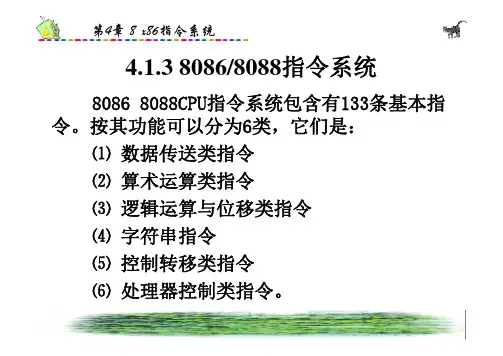
4.1.3 8086/8088指令系统8086/8088CPU指令系统包含有133条基本指令。
按其功能可以分为6类,它们是:⑴数据传送类指令⑵算术运算类指令⑶逻辑运算与位移类指令⑷字符串指令⑸控制转移类指令⑹处理器控制类指令。
一、数据传送类指令数据传送类指令时将数据、地址或立即数传送到寄存器或存储器单元中。
可完成寄存器与寄存器之间、寄存器与存储器之间、寄存器与I/O端口之间的字节或字传送。
它又可分为通用数据传送指令、输入/输出指令、目标地址传送指令和标志传送指令四组。
特点:除SAHF和POPF不影响标志寄存器内容。
(一)通用数据传送指令1. 最基本的传送指令指令格式及操作:MOV dst,src;(dst)←(src)将源操作数s指定的内容送到d目的操作数dst是目的操作数,它可以是存储器、通用寄存器(不能为IP)和段寄存器(不能为CS),不能为立即数。
Src是源操作数,它可以是存储器、通用寄存器、段寄存器和立即数。
MOVE指令需要注意的问题:①MOVE指令可传送8位数据,也可传送16位数据。
②MOVE指令中的两操作数s和d,必用1个寄存器,不允许同时为存储单元。
③不能用CS和IP做目的操作数。
④不允许段寄存器之间直接数据传送。
⑤不允许立即数做目的操作数。
⑥不能向段寄存器送立即数。
2.堆栈操作指令堆栈操作指令是用来完成压入和弹出堆栈操作的。
8086/8088指令系统中提供了完成这两种操作的相应指令。
⑴压入堆栈指令指令格式及操作:PUSH src;(SP) ←(SP)-2,((SP)+1:(SP)) ←(src) src源操作数可以是寄存器操作数和存储器操作数,且必须是16位的操作数,但不能是立即数。
⑵弹出堆栈指令指令格式及操作:POP dst; (dst) ←((SP)+1:(SP)),(SP) ←(SP)+2dst目的操作数可以是寄存器操作数和存储器操作数,且必须是16位的操作数,但不能是立即数。

2THE 80x86 MICROPROCESSOR2.1B RIEF HISTORY OF THE 80x86 FAMILY表2-1 Evolution of Intel’s Microprocessors实用文档实用文档2.2 I NSIDE THE 8088/8086图2-1 Internal Block Diagram of the 8088/86 CPU2.2.1 Pipelining流水线操作nonpipelined (e.g., 8085)pipelined (e.g., 8086)图2-2 Pipelined vs. Non-pipelined ExecutionIntel implemented the concept of pipelining in the 8088/86 by splitting the internal structure of microprocessor into two sections: the execution unit (EU) and the bus interface unit (BIU).The BIU accesses memory and peripherals while the EU executes instructions previously fetched. This works only if BIU keeps ahead of the EU, thus the BIU of the 8088/86 has a buffer. The buffer is 4 bytes long in the 8088 and 6 bytes in the 8086.If any instruction takes too long to execute, the queue is filled to its maximum capacity and the bus will set idle. The BIU fetches a new instruction whenever the queue has room for 2 bytes in the 6-byte 8086 queue, and for 1 byte in the 4-bytes 8088 queue.Pipelining in the 8088/86 has two stages: fetch and execution.2.2.2RegistersIn the CPU, register are used to store information temporarily.AX 16-bit register实用文档图2-3 register表2-2 Registers of the 8086/286 by Category实用文档2.3I NTRODUCTION TO ASSEMBLY PROGRAMMINGWhile the CPU can work only in binary, it can do so at very high speeds. However, it is quite tedious(单调乏味的)and slow for humans to deal with 0s and 1s in order to program the computer.A program that consists of 0s and 1s is called machine language, and in the early days of the computer, programmers actually coded programs in machine language.Eventually, assembly languages were developed, which provided mnemonics(记忆术) for the machine code instruction, plus other features that made programming faster and less prone to error. The term mnemonic is frequently used in computer science and engineering literature to refer to codes and abbreviations that are relatively easy to remember.Assembly language programs must be translated into machine code by a program called assembler.Assembly language is referred to a low-level language because it deals directly with the internal structure of the CPU.To program in assembly language, the programmer must be know the number of registers and their size, as well as other details of the CPU.实用文档Today, one can use many different programming languages, such as Pascal,BASIC, C, and numerous others. These languages are called high-level languages because the programmer does not have to be concerned with the internal details of the CPU. High-level languages are translated into machine code by a program called compiler.2.4I NTRODUCTION TO PROGRAM SEGMENTA typical assembly program consists of at least three segments:a code segmenta data segmenta stack segmentA segment is an area of memory that includes up to 64K bytes and begins on an address evenly divisible by 16 (such as an address ends in 0H).The segment size of 64K bytes came about because the 8085 microprocessor could address a maximum of 64K bytes of physical memory since it had only 16 pins for the address lines (216 = 64K). This limitation was carried into the design of the 8088/8086 to ensure compatibility.Whereas in the 8085 there was only 64K bytes of memory for all code, data,and stack information, in the 8088/86 there can be up to 64K bytes of memory 实用文档assigned to each category. Within an assembly language program, these categories are called the code segment, data segment, and stack segment. 2.4.1Logical address and physical addressIn Intel literature concerning the 8086, there are three types of addresses mentioned frequently:the physical addressthe offset addressthe logical addressThe physical address is the 20-bit address that is actually put on the address pins of 8086 microprocessor and decoded by the memory interfacing circuitry. The address can have a range of 00000H to FFFFFH. This is actual physical location in RAM or ROM within 1 megabyte memory range.The offset address is a location within a 64K-byte segment range. Therefore, an offset address can range from 0000H to FFFFH.The logical address consists of a segment value and an offset address. 2.4.2Code segmentThe code segment contains the assembly language instructions that 实用文档实用文档perform the tasks that the program was designed to accomplish.To execute a program, the 8086 fetch the instructions (opcode 操作码 and operand 操作数) from the code segment. The logical address of an instruction always consists of a CS and an IP , shown in CS:IP format.Assume values in CS and IP as shown in the diagram.:2. shift left CS3. add IP图2-4图2-5Example:If CS = 24F6H and IP = 634AH, show:(a) the logical address(b) the offset addressand calculate:(c) the physical address(d) the low range(e) the upper range of the code segment.Solution:(a) 24F6:634A(b) 634A(c) 2B2AA (24F60 + 634A)(d) 24F60 (24F60 + 0000)(e) 34F5F (24F60 + FFFF)2.4.3Logical address vs. physical address in the code segmentIn the code segment, CS and IP hold the logical address of the instructions to be executed. The following are the physical address and the contents of each location for a program. Remember that it is the physical address that is put on 实用文档实用文档the address bus by the 8086 CPU to be decoded by the memory circuitry.mov al, 57add ax, 1F35mov dh, 86mov dl, 72mov bh, al mov cx, dx mov bl, 9F mov ah, 20add ax, dx add cx, bx mnemonics and operand图2-62.4.4 Data segmentThe data segment is used to store information (data) that needs to be processed by the instructions in the code segment.实用文档IP图2-7Assume that DS is 5000 and the offset is 1950. Calculate the physical address of the byte.:2. shift left DS3. add offset图2-82.4.5Extra segmentES is a segment register used as an extra data segment. Although in many normal programs this is not used, its use is absolutely essential for string operations.2.4.6Stack segmentThe stack is a section of read/write memory (RAM) used by the CPU to store information temporarily.The CPU needs this storage area since there are only a limited number of registers. There must be some place for the CPU to store information safely and temporarily.Why not design a CPU with more registers?If the stack is a section of RAM, there must be registers inside the CPU to point to it. The two main registers used to access the stack are the SS (stack segment) register and the SP (stack pointer) register. These registers must be loaded before any instructions accessing the stack are used.Every registers inside the 80x86 (except segment registers and SP) can be stored in the stack and brought back into the CPU from the stack memory.实用文档The storing of a CPU register in the stack is called a push, and loading the contents into the CPU register is called a pop.Example of pushing onto stack:Assuming that SP = 1236, AX = 24B6, DI = 85C2, and DX = 5F93, show the contents of the stack as each of the following instructions:push axpush dipush dx实用文档startSP = 1236afterpush axSP = 1234afterpush diSP = 1232afterpush dxSP = 1230图2-9 Illustration of pushing the stackExample of popping the stack:Assuming that the stack is as shown below and SP = 18FA, show the contents of the stack registers as each of the following instructions is executed: pop cxpop dx实用文档实用文档pop cxstartSP = 18FAafter pop cx SP = 18FC CX = 1423after pop dx SP = 18FE DX = 2C6B after pop bx SP = 1900CX = F691图2-10 Illustration of popping the stack2.4.7 A few more words about segments in the 80x86Can a single physical address belong to many different logical addresses? YES! Look at the case of a physical address value of 15020H, there are manypossible logical addresses that represent this single physical address:表2-3 Many logical address and a single physical addressThis shows the dynamic behavior of the segment and offset concept in the 8086 CPU.One last point that must be clarified is the case when adding offset to the shifted segment register results in an address beyond the maximum allowed range of FFFFFH. In this situation, wrap-around will occur. This is shown in the following example:Example:What is the range of physical address if CS = FF59? (all values are in hex)实用文档实用文档Solution:The low range is FF590 (FF590 + 0000).The high range goes to FFFFF and wraps around, from 00000 to 0F58F (FF590 + FFFF = 10F58F), which is illustrated below:FF5900F58F00000FFFFF图2-11 Illustration of the wrap-around2.4.8 OverlappingIn calculating the physical address, it is possible that two segments can overlap, which is desirable in some circumstances. For example, overlapping is used in COM files.实用文档25000CS = 2500code SegmentstackSegmentdata Segment34FFF632107320F 82100920FFDS = 6321SS = 821030000CS = 3000code Segmentstack Segmentdata Segment 3FFFF 40500504FF 500005FFFFDS = 4050SS = 5000Nonoverlapping segments Overlapping segments图2-12 Nonoverlapping vs. overlapping segments图2-13 DOS window实用文档2.5 F lag register131211109876514154321R = reservedU = undefinedOF = overflow flag DF = direction flag IF = interrupt flag TF = trap flagSF = sign flag ZF = zero flagAF = auxiliary flag PF = parity flag CF = carry flag图2-14 Flag register2.5.1 CF, the Carry FlagThis flag is set whenever there is carry out, either from d7 after an 8-bit operation, or from d15 after from 16-bit operation.2.5.2 PF, Parity FlagAfter certain operations, the parity of the result ’s low-order byte is checked. If the byte has an even number of 1s, the parity flag is set to 1, otherwise it is cleared (set equal to zero).2.5.3 AF, Auxiliary FlagIf there is a carry from d3 to d4 of an operation, this bit is set, otherwise it is cleared. This flag is used by instructions that perform BCD (binary codeddecimal) arithmetic.2.5.4ZF, Zero FlagThe zero flag set to 1 if the result of arithmetic or logical operation is zero, otherwise, it is cleared.2.5.5SF, Sign FlagBinary representation of signed numbers uses the most significant bit as the sign bit. After arithmetic or logical operations the status of this sign bit is copied into the SF, thereby indicating the sign of the result.2.5.6TF, Trap FlagWhen this flag is set it allow the program to the single-step, meaning to execute one instruction at a time. Single-step is used for debugging purpose.2.5.7IF, Interrupt FlagThis flag is set or cleared to enable or disable only the external maskable interrupt requests.2.5.8DF, Direction FlagThis bit is used to control the direction of string operations实用文档2.5.9OF, Overflow FlagThis flag is set whenever the result of a signed number operation is too large, causing the high-order bit to overflow into the sign bit. In general, the carry flag is used to detect errors in unsigned arithmetic operations. The overflow flag is only used to detect errors in signed arithmetic operations. 2.5.10An example of the use of the flag bitsIn this section we examine the impact of the ADD instruction on the flag register.The flag bit affected by the ADD instruction are:CFPFAFZFSFOFExample:Show how the flag register is affected by the addition of 38H and 2FH.实用文档Solution:mov bh, 38h ;BH = 38Hadd bh, 2fh ;add 2F to BH, now BH = 67H38 0011 1000+ 2F 0010 1111-- ---------67 0110 0111CF = 0 since there is no carry beyond d7PF = 0 since there is an odd number of 1s in the result AF = 1 since there is a carry from d3 to d4ZF = 0 since the result is not zeroSF = 0 since d7 of the result is zeroExample:Show how the register is affected bymov al, 9ch ;AL = 9CHmov dh, 64h ;DH = 64Hadd al, dh ;now AL = 0实用文档Solution:9C 1001 1100+ 64 0110 0100-- ---------00 0000 0000CF = 1 since there is a carry beyond d7PF = 1 since there is an even number of 1s in the result AF = 1 since there is a carry from d3 to d4ZF = 1 since the result is zeroSF = 0 since d7 of the result is zeroExample:Show how the register is affected bymov ax, 34f5h ;AX = 34f5Hadd ax, 95ebh ;now AX = cae0hSolution:34f5 0011 0100 1111 0101实用文档+ 95eb 1001 0101 1110 1011---- -------------------cae0 1100 1010 1110 0000CF = 0 since there is no carry beyond d15PF = 0 since there is an odd number of 1s in the lower byteAF = 1 since there is a carry from d3 to d4ZF = 0 since the result is not zeroSF = 1 since d15 of the result is one2.680x86 ADDRESSING MODESThe CPU can access operands (data) in various ways, called addressing modes, the number of addressing modes is determined when the microprocessor is designed and cannot be changed. The 80x86 providers a total of seven distinct addressing modes:RegisterImmediateDirect实用文档Register indirectBased relativeIndexed relativeBased indexed relative2.6.1Register addressing mode寄存器寻址方式The register addressing mode involves the use of registers to hold the data to be manipulated. Memory is not accessed when this addressing mode is executed; therefore, it is relatively fast.Examples of register addressing mode follow:mov bx, dx ;copy the contents of DX into BXmov es, ax ;copy the contents of ES into AXadd al, bh ;add the contents of BH to contents of ALIt should be noted that the source and destination registers must be match in size. In other words coding ”mov cl, ax” will give an error, since the source is a 16-bit register and the destination is an 8-bit register.实用文档2.6.2Immediate addressing mode立即数寻址方式In the immediate addressing mode, the source operand is a constant. In immediate addressing mode, as the name implies, when the instruction is assembled, the operand comes immediately after the opcode. For this reason, this addressing mode executed quickly. However, in programming it has limited use. Immediate addressing mode can be used to load information into any of the registers except the segment registers and flag registers.Example:mov ax, 2550h ;move 2550h into AXmov cx, 625 ;load the decimal value 625 into CXmov bl, 40h ;load 40h into BLTo move information to the segment registers, the data must first be moved to a general-purpose registers and then to the segment register. Example:mov ax, 2550hmov ds, axmov ds, 0123h ;illegal!!!实用文档2.6.3Direct addressing mode直接寻方式In the direct addressing mode the data is in some memory location(s) andthe address of the data in memory comes immediately after the instruction.Note that in immediate addressing, the operand itself is provided with the instruction, whereas in direct addressing mode, the address of the operand is provided with the instruction. This address is the offset address and one can calculate the physical address by shifting left the DS register and adding it to the offset as follow:mov dl, [2400h] ;move contents of DS:2400h into DLIn this case the physical address is calculated by combining the contents of offset location 2400H with DS, the data segment register. Notice the bracket around the address. In absence of this bracket it will give an error since it is interpreted to move the value 2400H (16-bit data) into register DL, an 8-bit register.Example:Find the physical address of the memory location and its contents after theexecution of the following, assuming that DS = 1512H.实用文档mov al, 99hmov [3518h], alFirst AL is initialized to 99H, then in line two, the contents of AL are moved to logical address DS:3518H which is 1512H:3518H. Shifting DS left and adding it to the offset gives the physical address of 18638H (15120H + 3518H = 18638H). That means after the execution of the second instruction, the memory location with address 18368H will contain the value 99H.1512H:0000H 15120H1512H:0001H 15121H1512H:3518H 18638H图2-15 Illustration of the direct addressing mode2.6.4Register indirect addressing mode寄存器间接寻址方式In the register indirect addressing mode, the address of memory location where the operand resides is held by a register. The registers used for this实用文档purpose are SI, DI and BP, BX. If these three registers are used as pointers, that is, if they hold the offset of memory location, they must be combined with DS in order to generate the 20-bit physical address.Example:mov al, [bx] ;moves into AL the contents of the memory location;pointed to by DS:BX. Notice the BX is in bracket.mov cl, [si] ;move contents of DS:SI into CLmov [DI], ah ;move contents of AH into DS:DIExample:Assume that DS = 1120H, SI = 2498H, and AX = 17FEH. Show the contents of memory after the execution of:mov [si], axThe contents of AX are moved into memory locations with logical address DS:SI and DS:SI+1. Therefore, the physical address start at DS (shift left) + SI = 13698H, low address 13698H contains FEH, the low byte, and high address 13699H will contain 17H, the high byte.实用文档图2-16 Illustration of the register indirect addressing mode2.6.5Based relative addressing mode基址相对寻址方式In the based relative addressing mode, base registers BX and BP, as well as a displacement value, are used to calculate what is called effective address. The default segments used for the calculation of the physical address (PA) are DS for BX and SS for BP.Example:mov cx, [bx]+10h ;move DS:BX+10H and DS:BX+10H+1 into CX;PA = DS(shift left) + BX + 10HAlternative codings aremov cx, [bx+10h]实用文档andmov cx, 10h[bx]图2-17 Illustration of the based relative addressing mode Again the low address contents will go into CL and high address contents will go into CH.mov al, [bp]+5 ;PA = SS(shift left) + BP + 5mov al, [bp+5]mov al, 5[bp]2.6.6Indexed relative addressing mode变址相对寻址The indexed relative addressing mode works the same as based relative addressing mode, except that register DI and SI hold the offset address.实用文档Example:mov dx, [si]+5 ;PA = DS(shift left) + SI + 5mov cl, [di]+20 ;PA = DS(shift left) + DI + 20Example:Assume that DS = 4500H, SS = 2000H, BX = 2100H, SI = 1486H, DI = 8500H, BP = 7814H, and AX = 2512. Show the exact physical memory location where AX is stored in each the following, all values are in hex.(a) mov [bx]+20, ax(b) mov [si]+10, ax(c) mov [di]+4, ax(d) mov [bp]+12, axSolution:(a) DS:BX+20 PA = 45000 + 2100 + 20, location 47120 = (12) and 47121 = (25)(b) DS:SI+10 PA = 45000 + 1486 + 10, location 46496 = (12) and 46497 = (25)(c) DS:DI+4 PA = 45000 + 8500 + 4, location 4D504 = (12) and4D505 = (25)实用文档(d) S S:BP+12 PA = 20000 + 7814 + 12, location 27826 = (12) and 27827 = (25)2.6.7Based Indexed relative addressing mode基址加变址相对寻址方式By combining based and indexed relative addressing modes, a new addressing mode is derived called based indexed relative addressing mode. In this mode, one base register and one index register are used.Example:mov cl, [bx][di]+8 ;PA = DS(shift left) + BX + DI + 8mov ch, [bx][si]+20 ;PA = DS(shift left) + BX + SI + 20mov ah, [bp][di]+12 ;PA = SS(shift left) + BP + DI + 12mov ah, [bp][si]+29 ;PA = SS(shift left) + BP + SI + 29The coding of the instruction above can vary, for example, the last example could have been written:mov ah, [bp+si+29]ormov ah, [si+bp+29] ;the register order does not matter实用文档2.6.8Segment overrides段超越表2-4 Offset Registers for Various SegmentsTable 表2-4 provides a summary of the offset registers that can be used with the four segment registers of 80x86. The 80x86 CPU allows the program to override the default segment and use any segment register. To do that, specify the segment in code. For example:表2-5 Sample Segment Overrides实用文档2.6.9Summary of 80x86 Addressing Modes表2-6 Summary of 80x86 addressing modes实用文档实用文档。
西安电子科技大学《微型计算机原理》课程设计题目基于8086的步进电机控制学生姓名专业班级11级计嵌班学号 201院(系)信息工程学院指导教师完成时间年月日目录1 课程设计的目的 (1)2课程设计的任务与要求 (1)3引言 (1)4设计方案与论证 (2)5 设计内容及功能说明 (3)5.1 励磁线圈及其励磁顺序 (3)5.2工作原理 (4)5.3 8086 CPU (5)5.4 8255工作方式选择 (6)5.5 ULN2003A (6)5.6 74LS273 (7)5.7 74LS138 (7)6单元电路的设计(计算与说明) (7)7硬件的制作与调试 (10)8总结 (12)参考文献 (13)附录1:总体电路原理图 (14)附录2:元器件清单 (14)附录3:源程序代码 (15)1 课程设计的目的培养和锻炼学生在学习完本门课后综合应用所学理论知识,解决实际工程设计和应用问题的能力的重要教学环节。
要求学生熟悉和掌握微机系统的软件、硬件设计的方法、设计步骤,使学生得到微机开发应用方面的初步训练。
让学生独立或集体讨论设计题目的总体设计方案、编程、软件硬件调试、编写设计报告等问题,真正做到理论联系实际,提高动手能力和分析问题、解决问题的能力,实现由学习知识到应用知识的初步过渡。
通过本次课程设计使学生熟练掌握微机系统与接口扩展电路的设计方法,了解步进电机控制的基本原理,掌握控制步进电机转动的编程方法,进一步熟练掌握8255A并行I/O口的工作方式以及编程方法,熟练应用8086以及汇编语言编写应用程序和实际设计中的硬软件调试方法和步骤,熟悉微机系统的硬软件开发工具的使用方法。
体会系统整体设计的流程与方法,为以后系统级设计积累经验。
培养学生在实际的工程设计中查阅资料,撰写设计报告表达设计思想和结果的能力。
2 课程设计的任务与要求01.通过开关K1实现步进电机的开始与停止;02. 通过开关K2来选择步进电机的正转与反转;03. 通过开关K3,K4组成(2-4译码)四档电机转速选择;04. 对每只开关的选择情况同时通过4位8段数码管来显示;05. 扩展设计:可以在以上功能基础上,增加控制步进电机单步转动的开关;增加控制电机加速转动的开关;增加控制电机减速的开关。
微机原理课程基于80x86的步进电机控制系统《微机原理与接口技术》课程设计姓名:厉小洋学号:0945533117班级:09电气1班专业:电气工程及其自动化学院:电气与信息工程学院江苏科技大学张家港校区2012年9月目录一理论部分 (2)1课题要求与内容 (2)2 系统方案设计 (3)3 系统硬件的设计 (4)4 系统软件设计 (5)二实践部分 (6)1 系统硬件原理简介 (6)2 系统硬件调试中出现的问题及解决措施 (10)3 系统软件 (11)3.1 软件设计 (11)3.2软件调试中出现的问题及解决措施 (14)三附录 (15)题目:《基于80x86的步进电机控制系统》第一章、理论部分一微机原理课程设计课题要求与内容内容要求:(1)使用8255A控制步进电机的运转。
(2)使用数码管LED显示速度的大小。
(3)使用8253定时器调节速度的大小。
(4)使用4个独立按键控制步进电机,即“正传”、“反转”、“停止”、“调速”。
(5)使用8259A产生中断控制按键;(6)使用DAC0832显示速度的波形。
拓展功能:(1)按键部分可以增加“加速”、“减速”等功能;(2)考虑可以加蜂鸣器来区分“正转”和“反转”;(3)其他可以有自己特色的功能均可。
二系统方案设计在课程要求的前提下,步进电机为四相八拍步进电机,这样可以用8255的一个端口控制电机的驱动,LED显示为十六位图1系统流程图在8255中可用两个端口控制,按键单元可与电机共用一个八位端口,由8254产生可编程脉冲,进入8259产生中断,反馈给80x86,控制8255。
再执行到步进电机及其LED显示上,一个脉冲步进电机一拍。
由按键读入系统状态。
具体的系统设计如图1为系统概况流程图三系统硬件设计在硬件设计中,主要是通过步进电机模块、8255模块、LED模块、8254模块。
在8255芯片上用A,B口控制数码管的显示(A为位选B为段选),C口的高四位为四个按键单元,低四位作为输出,控制步进电机。
片选CS接IOY2。
在8259和8254上,采用一个脉冲一拍的方式。
给8254一个1.8432MHZ在CLK2,OUT2输出给CLK0,由OUT0给8259的INT,输出一个脉冲,经由IR0给80x86的中断口INTR。
如图2为硬件连接图,如下硬件连接:8254,8255,8259的CS分别接在IOY2,IOY0,IOY18255芯片连接:8255的A,B控制LED,A口接位选,B口接段选,将C 口分为两段,高四位读取按键,低四位控制步进电机,按键分为四个如下表1所示图2硬件连接图四系统软件设计图3软件系统工作流程图过8255读取按键的信号,来控制步进电机的开关,正转,反转,速度的大小。
通过8254计数器工作在方式0的状态下来控制每拍运行的时间,步进电机速度不同,赋给8254的初始值不同,同时8255的PA,PB口向LED接口输出信号,LED数码管显示步进电机每分钟的转速。
8254计数器每次运行结束,向8259发出一个高电平,8259IR0接口检测到高电平信号,即进入中断服务程序,在中断服务程序里,执行对下一拍给步进电机信号的赋值。
在每次循环中,执行键盘按键检测程序,如有按键,退出程序,否则,反复循环。
如图3为软件系统的工作流程图第二章实践部分一系统硬件原理简介1.1步进电机的简介及其工作原理步进电机的驱动原理是通过它每相线圈的电流的顺序切换来使电机作步进式旋转,驱动电路由脉冲来控制,所以调节脉冲的频率便可改变步进电机的转速,微控制器最适合控制步进电机。
另外,由于电机的转动惯量的存在,其转动速度还受驱动功率的影响,当脉冲的频率大于某一值时,电机便不再转动。
本次课程设计中电机共有四个相位(A,B,C,D),按转动步骤可分单4拍(A->B->C->D->A),双4拍(AB->BC->CD->DA->AB)和单双8拍(A->AB->B->BC->C->CD->D->DA->A).此模块的主要功能是通过接收8255的C口输入信号来控制步进电机的转动,A,B,C,D分别代表不同的四个相位,分别接入到PC0,PC1,PC2和PC3实现转动控制表 2如上述表2所示,通过编程对8255的输出进行控制,使输出按照相序表给驱动电路供电,则步进电机的输入也和相序表一致,这样步进电机就可以正向转动,反之,则反向转动。
1.2实验所用芯片的介绍及其控制方式1.2.1 8254的简介8254是Intel公司生产的课可编程定时器,8254芯片主要由四部分组成:1 数据总线缓冲器数据总线缓冲器是一个三态、双向8位寄存器主要作用是与CPU进行数据交换,8位数据线D7~D0与CPU的系统数据总线连接,构成CPU和8254之间信息传送的通道,CPU通过数据总线缓冲器向8254写入控制命令、计数初始值或读取计数值。
2 读写逻辑读写逻辑是芯片的控制部分,编程人员通过控制信号的选择来选择芯片的工作方式。
读/写控制逻辑用来接收CPU系统总线的读、写控制信号和端口选择信号,用于控制8254内部寄存器的读/写操作。
3 控制字寄存器控制寄存器是一个只能写不能读的8位寄存器,系统通过指令将控制字写入控制寄存器,设定8254的不同工作方式。
4 计数器8254内部有三个结构完全相同而又相互独立的16位减“1”计数器,每个计数器有六种工作方式,各自可按照编程设定的方式工作。
1).有3个独立的16位计数器2).每个计数器可按十进制或二进制计数3).8254每个计数器允许最高计数为10MHZ4).8254 有读回指令,还可以读出状态寄存器的内容5).每个计数器可编程工作于6中不同的方式6)计数脉冲可以是有规律的时钟信号,也可以是随机信号,计数初值公式为n=fclki/fouti(fclki是输入时钟脉冲的频率,fouti是输出波形的频率)工作方式的分类:1)方式0:计数到0结束输出正跳跃信号方式2)方式1:硬件可重触发单稳方式3)方式2:频率发生器4)方式3:方波发生器5)方式4:软件触发选通方式6)方式5:硬件触发选通方式8254的控制字有两个:一个用来设置计数工作方式称为方式控制字。
另一个用来设置读回命令,称为读回控制字。
如下表3是控制方式表格表3 8254的方式控制字格式8255的简介及其控制8255是Intel公司生产的可编程并行I/O接口芯片,有3个8位并行I/O 口。
具有3个通道3种工作方式的可编程并行接口芯片(40引脚)。
其各口功能可由软件选择,使用灵活,通用性强。
8255可作为单片机与多种外设连接时的中间接口电路。
8255作为主机与外设的连接芯片,必须提供与主机相连的3个总线接口,即数据线、地址线、控制线接口。
同时必须具有与外设连接的接口A、B、C口。
由于8255可编程,所以必须具有逻辑控制部分,因而8255内部结构分为3个部分:与CPU连接部分、与外设连接部分、控制部分。
8255可编程外围接口芯片是通用并行口芯片,具有A、B、C三个并行接口,有三种工方式。
方式0——基本的输入输出。
方式1——选通输入输出。
方式2——双选通工作方式表格2为控制字格式,如下图4 、图5分别为8255工作方式控制字格式和8255 C口按位置位/复位控制字格式。
图4、8255工作方式控制字格式图5 8255 C口按位置位/复位控制字格式8259的简介及其控制方式8259A是专门为了对8085A和8086/8088进行中断控制而设计的芯片,它是可以用程序控制的中断控制器。
单个的8259A能管理8级向量优先级中断。
在不增加其他电路的情况下,最多可以级联成64级的向量优级中断系统。
8259A有多种工作方式,能用于各种系统。
各种工作方式的设定是在初始化时通过软件进行的。
在总线控制器的控制下,8259A芯片可以处于编程状态和操作状态,编程状态是CPU使用IN或OUT指令对8259A芯片进行初始化编程的状态。
功能:就是在有多个中断源的系统中,接受外部的中断请求,并进行判断,选中当前优先级最高的中断请求,再将此请求送到CPU的INTR端;当CPU响应中断并进入中断子程序的处理过程后,中断控制器仍负责对外部中断请求的管理。
二系统硬件调试中出现的问题及解决措施问题一步进电机运转不流畅原因:分析后发现,程序执行中的中断无法连续执行,因为8254采用方式3发出的中断信号,脉冲时间太短,解决方法:在调整8254的计数器采用方式1后,一旦检测信号,重新将计数器装入初值问题二数码管显示乱码原因:查看显示数据发现,当8255输出一个段码后,下一次出现的是上一次输出的值解决方法:在以后每次输出之后,都输出一个00A,以清除8255寄存器中的值,以达到清除乱码的效果问题三程序执行中有计数器赋初值,所以每次计数器都不能执行完发出中断原因:赋初值在循环当中解决方法:将计数器赋初值放到循环外面,引用FLAG来判断是否进入中断,如果进入,则重新将计数器赋初值问题四:读取按键混乱原因:用PC7-PC4来读取按键。
读出的按键数值在高四位,于我们用低四位处理相冲突解决方法:将读出的数值右移四位三系统软件3.1 软件设计3.1.1 8255控制模块如图6所示,8255主要负责不停的读取按键状态检测速度的大小。
口2如图6 8255流程图3.1.2 8254延时模块设置8254的控制字,通过8254设置延时,产生延时频率,最后再接入到8255控制步进电机的运转与停止,速度大小主要通过对8254装入初值的不同来控制,流程如下图7,与上图6衔接(图7分别于图6最后连接)1PC7图7 8254模块流程3.1.3 LED显示模块LED模块的主要功能是前四位显示步进电机的转速(r/min)度的值。
此模块用8255A、B口的控制LED数码管的位码,采用动态扫描方式让数码管显示出速度值。
利用8255的端口A、B口各八位,共十六位控制数码管的显示,其中A 口为位选控制,B口为段选控制,直接显示步进电机的转速。
数码管的显示控制对应于下图8图8 数码管对应图3.1.4 8259中断模块中断模块的82598254的信号产生中断,给步进电机,如图9图93.2软件调试中出现的问题及解决措施问题一程序运行中反复执行MOV BX,OFFSET TTABLEL.原因:放在最高的级别的大循环当中,所以会反复执行。
解决方法:引用CX计数,当CX由08H变成00H时,才返回执行MOV BX,OFFSET TTABLEL问题二跳转指令无法达到期望位置,提示错误。
原因:JZ,JNZ指令只能跳转255,而我们程序跳转跳远,超出范围。
解决方法:使用JMP语句,在中间插入,多次跳转,以达到跳转位置附录(源程序)IOY1 EQU 3040H ;片选IOY0对应的端口始地址MY8255_A EQU IOY1+00H*4 ;8255的A口地址MY8255_B EQU IOY1+01H*4 ;8255的B口地址MY8255_C EQU IOY1+02H*4 ;8255的C口地址MY8255_MODE EQU IOY1+03H*4 ;8255的控制寄存器地址IOY2 EQU 3080H ;片选IOY1对应的端口始地址MY8254_COUNT0 EQU IOY2+00H*4 ;8254计数器0端口地址MY8254_COUNT1 EQU IOY2+01H*4 ;8254计数器1端口地址MY8254_COUNT2 EQU IOY2+02H*4 ;8254计数器2端口地址MY8254_MODE EQU IOY2+03H*4 ;8254控制寄存器端口地址INTR_IVADD EQU 01C8H ;INTR对应的中断矢量地址INTR_OCW1 EQU 0A1H ;INTR对应PC机内部8259的OCW1地址INTR_OCW2 EQU 0A0H ;INTR对应PC机内部8259的OCW2地址INTR_IM EQU 0FBH ;INTR对应的中断屏蔽字IOY0 EQU 3000H ;片选IOY0对应的端口始地址MY8259_ICW1 EQU IOY0+00H ;实验系统中8259的ICW1端口地址MY8259_ICW2 EQU IOY0+04H ;实验系统中8259的ICW2端口地址MY8259_ICW3 EQU IOY0+04H ;实验系统中8259的ICW3端口地址MY8259_ICW4 EQU IOY0+04H ;实验系统中8259的ICW4端口地址MY8259_OCW1 EQU IOY0+04H ;实验系统中8259的OCW1端口地址MY8259_OCW2 EQU IOY0+00H ;实验系统中8259的OCW2端口地址MY8259_OCW3 EQU IOY0+00H ;实验系统中8259的OCW3端口地址STACK1 SEGMENT STACKDW 256 DUP(?)STACK1 ENDSDATA SEGMENTMES DB 'Press any key to exit!',0AH,0DH,0AH,0DH,'$'CS_BAK DW ? ;保存INTR原中断处理程序入口段地址的变量IP_BAK DW ? ;保存INTR原中断处理程序入口偏移地址的变量IM_BAK DB ? ;保存INTR原中断屏蔽字的变量TTABLE1 DB 01H,03H,02H,06H,04H,0CH,08H,09H ;正转编码TTABLE2 DB 09H,08H,0CH,04H,06H,02H,03H,01H ;反转编码FLAG DB 00H ;标志位DATA ENDSCODE SEGMENTASSUME CS:CODE,DS:DATASTART: MOV AX,DATAMOV DS,AXMOV DX,OFFSET MES ;显示退出提示MOV AH,09HINT 21HCLIMOV AX,0000H ;替换INTR的中断矢量MOV ES,AXMOV DI,INTR_IVADDMOV AX,ES:[DI]MOV IP_BAK,AX ;保存INTR原中断处理程序入口偏移地址MOV AX,OFFSET MYISRMOV ES:[DI],AX ;设置当前中断处理程序入口偏移地址ADD DI,2MOV AX,ES:[DI]MOV CS_BAK,AX ;保存INTR原中断处理程序入口段地址MOV AX,SEG MYISRMOV ES:[DI],AX ;设置当前中断处理程序入口段地址MOV DX,INTR_OCW1 ;设置中断屏蔽寄存器,打开INTR 的屏蔽位IN AL,DXMOV IM_BAK,AL ;保存INTR原中断屏蔽字AND AL,INTR_IMOUT DX,ALMOV DX,MY8259_ICW1 ;初始化实验系统中8259的ICW1MOV AL,13H ;边沿触发、单片8259、需要ICW4OUT DX,ALMOV DX,MY8259_ICW2 ;初始化实验系统中8259的ICWMOV AL,08HOUT DX,ALMOV DX,MY8259_ICW4 ;初始化实验系统中8259的ICW4MOV AL,01H ;非自动结束EOIOUT DX,ALMOV DX,MY8259_OCW3 ;向8259的OCW3发送读取IRR 命令MOV AL,0AHOUT DX,ALMOV DX,MY8259_OCW1 ;初始化实验系统中8259的OCW1MOV AL,0FEH ;打开IR0的屏蔽位OUT DX,ALSTIMOV DX,MY8255_MODE ;初始化8255工作方式MOV AL,88H ;工作方式0,A口输出,B口输出,C高四位输入,低四位输出OUT DX,ALA:MOV AH,1 ;判断是否有按键按下INT 16HJNZ WAIT1 ;无按键则跳回继续执行,有则退出MOV CX,08H ;计数初值MOV DX,MY8255_CIN AL,DX ;读C口高4位的数据SHR AL,1 ;转向C口的低4位SHR AL,1SHR AL,1SHR AL,1PUSH BXMOV BL,AL ;BL保存AL中的数据MOV BH,BL ;BH中保存AL的数据AND BL,01H ;取开关状态CMP BL,00HJZ A ;如果是0,则跳转到AAND BH,02H ;取正反转状态CMP BH,00HJZ FORWARD ;如果是0,跳正转JNZ BACKWARD ;如果是1,跳反转POP BXFORWARD:MOV BX,OFFSET TTABLE1 ;将的TTABLE1首地址赋给BXJMP B ;跳转到B取速度BACKWARD:MOV BX,OFFSET TTABLE2 ;将的TTABLE2首地址赋给BXJMP B ;跳转到B取速度B: MOV CX,08H ;计数初值MOV FLAG,00H ;中断结束后给FLAG赋值00HMOV DX,MY8255_CIN AL,DX ;读C口数据SHR AL,04H ;将数据左移四位AND AL,0CH ;取高两位MOV AH,AL ;保存AL中的数据AND AL,08H ;取最高位CMP AL,00H ;与00比较JZ CAMP1JNZ CAMP2CAMP1: AND AH,04H ;取第二位CMP AH,00HJZ SPEED1C ;00速度1, 跳SPEED1CJNZ SPEED2C ;01速度2,跳SPEED2C CAMP2: AND AH,04H ;取第二位CMP AH,00HJZ SPEED3C ;10速度3,跳SPEED1CJNZ SPEED4C1 ;11速度4,跳SPEED1C SPEED1C:MOV DX,MY8254_MODE ;初始化8254工作方式MOV AL,0B6H ;计数器2,方式3OUT DX,ALMOV DX,MY8254_COUNT2 ;装入计数初值MOV AL,24H ;36分频OUT DX,ALMOV AL,00HOUT DX,ALMOV DX,MY8254_MODE ;初始化8254工作方式MOV AL,30H ;计数器0,方式1OUT DX,ALMOV DX,MY8254_COUNT0 ;装入计数初值MOV AL,0FFH ;255OUT DX,ALMOV AL,00HOUT DX,ALJMP SPEED1SPEED2C:MOV DX,MY8254_MODE ;初始化8254工作方式MOV AL,0B6H ;计数器2,方式3OUT DX,ALMOV DX,MY8254_COUNT2 ;装入计数初值MOV AL,48H ;72分频OUT DX,ALMOV AL,00HMOV DX,MY8254_MODE ;初始化8254工作方式MOV AL,36H ;计数器0,方式1OUT DX,ALMOV DX,MY8254_COUNT0 ;装入计数初值MOV AL,0FFH ;255OUT DX,ALMOV AL,00HOUT DX,ALJMP SPEED2A1: JMP ASPEED4C1:JMP SPEED4SPEED3C:MOV DX,MY8254_MODE ;初始化8254工作方式MOV AL,0B6H ;计数器2,方式3OUT DX,ALMOV DX,MY8254_COUNT2 ;装入计数初值MOV AL,90H ;144分频OUT DX,ALMOV AL,00HOUT DX,ALMOV DX,MY8254_MODE ;初始化8254工作方式MOV AL,36H ;计数器0,方式1OUT DX,ALMOV DX,MY8254_COUNT0 ;装入计数初值MOV AL,0FFH ;255OUT DX,ALMOV AL,00HOUT DX,ALJMP SPEED3SPEED4C:MOV DX,MY8254_MODE ;初始化8254工作方式MOV AL,0B6H ;计数器2,方式3OUT DX,ALMOV DX,MY8254_COUNT2 ;装入计数初值MOV AL,0FFH ;288分频OUT DX,ALOUT DX,ALMOV DX,MY8254_MODE ;初始化8254工作方式MOV AL,36H ;计数器0,方式1OUT DX,ALMOV DX,MY8254_COUNT0 ;装入计数初值MOV AL,0FFH ;255OUT DX,ALMOV AL,00HOUT DX,ALJMP SPEED4A2: JMP A1SPEED1:MOV AL,[BX]MOV DX,MY8255_C ;给步进电机输入信号OUT DX,ALDEC CX ;每输入一次信号CX减1CMP CX,00H ;将CX的值与00H比较,如果跳转8次,跳转到A,重新开始扫描按键JZ ACMP FLAG,OOH ;判断是不是已经进入中断,如果进入,跳转到B,如果没有,继续执行LED的显示JNZ BMOV DX,MY8255_AMOV AL,0EFH ;段选3号位OUT DX,ALMOV DX,MY8255_BMOV AL,06H ;显示数字1OUT DX,ALMOV AL,00H ;消除锁存值OUT DX,ALMOV DX,MY8255_AMOV AL,0F7H ;段选2号位OUT DX,ALMOV DX,MY8255_BMOV AL,5BH ;显示数字2OUT DX,ALMOV AL,00H ;消除锁存值OUT DX,ALMOV DX,MY8255_AMOV AL,0FBH ;段选1号位OUT DX,ALMOV DX,MY8255_BMOV AL,3FH ;显示数字0OUT DX,ALMOV AL,00H ;消除锁存值OUT DX,ALJMP A1A3: JMP A2SPEED2:MOV AL,[BX]MOV DX,MY8255_C ;给步进电机输入信号OUT DX,ALDEC CX ;每输入一次信号CX减1CMP CX,00H ;将CX的值与00H比较,如果跳转8次,跳转到A,重新开始扫描按键JZ ACMP FLAG,OOH ;判断是不是已经进入中断,如果进入,跳转到B,如果没有,继续执行LED的显示JNZ BMOV DX,MY8255_AMOV AL,0F7H ;段选2号位OUT DX,ALMOV DX,MY8255_BMOV AL,7DH ;显示数字6OUT DX,ALMOV AL,00H ;消除锁存值OUT DX,ALMOV DX,MY8255_AMOV AL,0FBH ;段选1号位OUT DX,ALMOV DX,MY8255_BMOV AL,3FH ;显示数字0OUT DX,ALMOV AL,00H ;消除锁存值OUT DX,ALJMP A2SPEED3:MOV AL,[BX]MOV DX,MY8255_C ;给步进电机输入信号OUT DX,ALDEC CX ;每输入一次信号CX减1CMP CX,00H ;将CX的值与00H比较,如果跳转8次,跳转到A,重新开始扫描按键JZ ACMP FLAG,OOH ;判断是不是已经进入中断,如果进入,跳转到B,如果没有,继续执行LED的显示JNZ BMOV DX,MY8255_AMOV AL,0F7H ;段选2号位OUT DX,ALMOV DX,MY8255_BMOV AL,4FH ;显示数字3OUT DX,ALMOV AL,00H ;消除锁存值OUT DX,ALMOV DX,MY8255_AMOV AL,0FBH ;段选1号位OUT DX,ALMOV DX,MY8255_BMOV AL,3FH ;显示数字0OUT DX,ALMOV AL,00HOUT DX,ALJMP A3A4: JMP A3SPEED4:MOV AL,[BX]MOV DX,MY8255_COUT DX,ALDEC CX ;每输入一次信号CX减1CMP CX,00H ;将CX的值与C00H比较,如果跳转8次,跳转到A,重新开始扫描按键JZ ACMP FLAG,OOH ;判断是不是已经进入中断,如果进入,跳转到B,如果没有,继续执行LED的显示JNZ BMOV DX,MY8255_AMOV AL,0F7H ;段选2号位OUT DX,ALMOV DX,MY8255_BMOV AL,06H ;显示数字5OUT DX,ALMOV AL,00H ;消除锁存值OUT DX,ALMOV DX,MY8255_AMOV AL,0FBH ;段选1号位OUT DX,ALMOV DX,MY8255_BMOV AL,6DHOUT DX,AL ;显示数字1MOV AL,00HOUT DX,AL ;消除锁存值JMP A4QUIT: CLIMOV AX,0000H ;恢复INTR原中断矢量MOV ES,AXMOV DI,INTR_IVADDMOV AX,IP_BAK ;恢复INTR原中断处理程序入口偏移地址MOV ES:[DI],AXADD DI,2MOV AX,CS_BAK ;恢复INTR原中断处理程序入口段地址MOV ES:[DI],AXMOV DX,INTR_OCW1 ;恢复INTR原中断屏蔽寄存器的屏蔽字MOV AL,IM_BAKOUT DX,ALSTIMOV AX,4C00H ;返回到DOSINT 21HMYISR PROC NEAR ;中断处理程序MYISR PUSH AXIR0ISR:MOV AL,30H ;IR0处理,显示字符串STR0 MOV AH,0EHINT 10HMOV AL,20HINT 10HINC BX ;列表向后移一格MOV FLAG,01HJMP OVEROVER: MOV DX,INTR_OCW2 ;向试验箱上8259发送中断结束命令MOV AL,20HOUT DX,ALMOV AL,20H ;向PC机内部8259发送中断结束命令OUT 20H,ALPOP AXIRETMYISR ENDPCODE ENDSEND START。