基于蓝牙低功耗的4.1mcu解决方案
- 格式:docx
- 大小:22.40 KB
- 文档页数:16
MCU低功耗的三种实现方法近年消费性电子商品与计算机产品隔阂日小,从最现实的角度来看,智慧生活的抬头、让消费性电子产品功能需求越来越高、设计越来越复杂,在在制造了品牌商不得不采用低功秏MCU 的契机。
为了让控制器的耗电量达到最低。
达成的方式大概有以下三种:降低工作模式时的功秏、减少休眠模式的功秏、以及缩短由休眠到工作的唤醒时间。
工作模式时的功秏减低是最先被克服的任务,目前推出低功秏MCU 的厂商多半已经做到。
其中最大眉角在于,必须利用较低的系统频率或运行电压来节省功耗,但是不可以影响到产品的效能。
整合电源管理是一个不错的方法,在此领域有着墨的厂商如TI,ST,Silicon Labs 都有相应措施。
Silicon Labs 微控制器产品营销总监Mike Salas 表示,整合专有的DC-DC 转换器,可以让运作模式的操作电压降至0.9V,原本必须使用2 颗电池才能操作、也可因此而只要1 颗就能使用相同功能。
而休眠模式的功秏控制,业界的共识可分成两方向:向下压低休眠时的最低功秏,以及,提供不同等级的待机模式。
意法半导体大中华暨南亚区产品营销经理杨正廉说,现在的低功耗MCU 可以针对不同的省电模式进行动态调整,依据使用状况不同,自动关闭不需要的功能,至低的功耗仅0.27A,几乎是个电表无法侦测出来的数字。
从终端产品的角度看,需要低功秏MCU,许多是属于长时间休眠状态、但是只要需要工作,就必须迅速站上岗位开始运作,最简单的例子就是烟雾侦测器。
从MCU 本身的设计来看,从休眠到运作的转换时间如果太长,等于白白浪费了等候期间的电流损耗。
所以,要从低功耗到超低功耗,一分一秒都得锱铢必较。
低功耗蓝牙解决方案
《低功耗蓝牙解决方案》
随着物联网技术的发展,低功耗蓝牙(BLE)技术在智能家居、智能穿戴、智能健康和其他领域中得到了广泛应用。
然而,尽管低功耗蓝牙技术可以实现设备之间的低功耗连接,但是在实际应用中,仍然存在着一些问题需要解决。
为了解决低功耗蓝牙技术在实际应用中的问题,一些厂家和研发机构提出了一些解决方案。
首先,通过优化蓝牙模块的硬件设计和功耗管理的算法,可以降低设备的功耗,延长设备的使用时间。
其次,通过对BLE协议栈的优化,可以提高数据传
输效率,减少蓝牙连接时的能耗。
另外,还可以使用低功耗蓝牙模块进行数据的缓存和离线处理,从而减少设备与手机之间的通信次数,降低功耗。
除此之外,低功耗蓝牙技术的开发者和使用者还可以根据具体的应用场景,选择合适的BLE解决方案。
例如,在智能家居
领域,可以采用低功耗蓝牙Mesh网络,实现多个设备之间的
互联互通。
在智能健康领域,可以利用低功耗蓝牙的定位功能和传感器技术,实现对用户健康数据的实时监测和采集。
总之,通过不断优化硬件设计、算法和协议栈,以及根据不同的应用场景选择合适的解决方案,可以有效解决低功耗蓝牙技术在实际应用中的问题,实现设备之间的低功耗连接和高效能传输。
这些努力将进一步推动低功耗蓝牙技术在物联网领域的广泛应用。
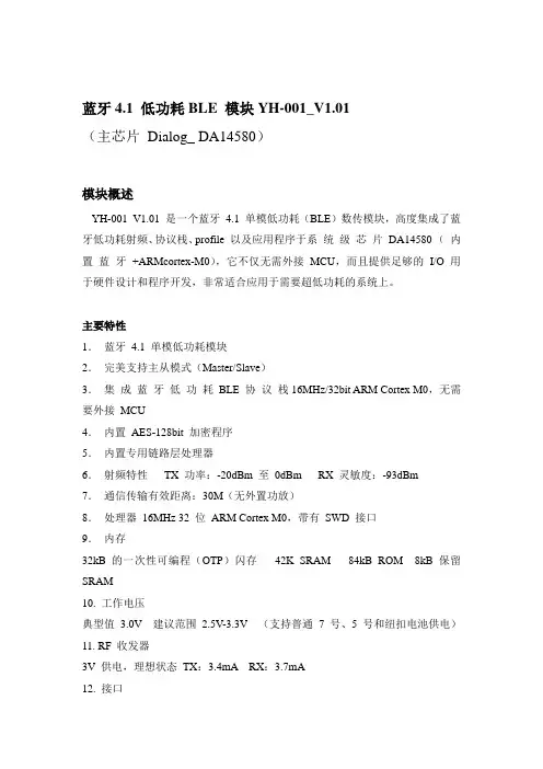
蓝牙4.1 低功耗BLE 模块YH-001_V1.01(主芯片Dialog_ DA14580)模块概述YH-001_V1.01 是一个蓝牙4.1 单模低功耗(BLE)数传模块,高度集成了蓝牙低功耗射频、协议栈、profile 以及应用程序于系统级芯片DA14580 (内置蓝牙+ARMcortex-M0),它不仅无需外接MCU,而且提供足够的I/O 用于硬件设计和程序开发,非常适合应用于需要超低功耗的系统上。
主要特性1.蓝牙4.1 单模低功耗模块2.完美支持主从模式(Master/Slave)3.集成蓝牙低功耗BLE 协议栈16MHz/32bit ARM Cortex M0,无需要外接MCU4.内置AES-128bit 加密程序5.内置专用链路层处理器6.射频特性TX 功率:-20dBm 至0dBm RX 灵敏度:-93dBm7.通信传输有效距离:30M(无外置功放)8.处理器16MHz 32 位ARM Cortex M0,带有SWD 接口9.内存32kB 的一次性可编程(OTP)闪存42K SRAM 84kB ROM 8kB 保留SRAM10. 工作电压典型值3.0V 建议范围 2.5V-3.3V (支持普通7 号、5 号和纽扣电池供电)11. RF 收发器3V 供电,理想状态TX:3.4mA RX:3.7mA12. 接口4 通道10 位ADC 2 个UART 接口SPI 接口I2C 接口PWM 输出20 通用I/O 接口13. 封装尺寸23.2mm * 17mm * 1.8mm应用领域:1.医疗保健设备2.运动及健康设备3.家庭智能设备4.手机和PC 配件5.工业自动化设备6. 物联网节点设备及网关7. 智能遥控器(含语音识别)8. 手机APP 控制互动玩具9. 手机APP 控制四轴飞行器10.HID 外设,键盘、鼠标……YH-001_V1.01 方框图YH001-V1.01电气特性:绝对最大额定值建议工作条件NOTE1:基于蓝牙芯片RAM 工作特性,要求蓝牙设备冷启动时VDD ≧2.5 V,所以建议模块供电稳定VDD=3V外形尺寸:YH-001_V1.01 的总体尺寸,长23.2 毫米,宽17 毫米,厚1.8 毫米。
Intel MCU方案概述本文档介绍了英特尔(Intel)微控制器单元(MCU)方案的基本概念、特点和应用。
我们将重点介绍Intel MCU方案的架构、功能和性能优势,以及适用的应用领域和案例。
什么是Intel MCU方案Intel MCU方案是一种集成电路方案,由英特尔设计和制造。
该方案集成了微控制器单元,具备高性能计算和低功耗特性。
它是一种强大的嵌入式解决方案,适用于多种应用领域。
架构和功能1. 核心处理器Intel MCU方案使用先进的x86架构作为核心处理器。
这种架构提供高性能计算能力和广泛的软件生态系统支持。
x86架构还提供了多核处理器和多线程处理技术,以满足高性能和并发处理需求。
2. 基于固件的管理功能Intel MCU方案提供了基于固件的管理功能,包括远程管理、安全引导和固件升级等。
这些功能可以帮助系统管理员远程监控和管理设备,提高设备的可靠性和安全性。
3. 低功耗设计Intel MCU方案采用了先进的低功耗设计技术,包括功耗管理、睡眠模式和动态调频等。
这些技术可以显著降低系统的功耗,延长设备的电池寿命。
4. 丰富的连接性Intel MCU方案支持多种通信接口和协议,如WiFi、蓝牙、USB和以太网等。
这些接口和协议可以帮助设备方便地与其他设备和互联网进行通信,实现智能互联。
5. 强大的图形处理能力Intel MCU方案配备了先进的图形处理器(GPU),支持高清视频播放和3D游戏等图形应用。
这种强大的图形处理能力可以为用户提供更好的视觉体验。
应用领域Intel MCU方案广泛应用于各种嵌入式系统和终端设备。
以下是一些典型的应用领域:1. 智能家居Intel MCU方案可以用于智能家居系统,实现家庭自动化和远程控制。
例如,通过与智能家居网关配合使用,用户可以通过手机远程控制家庭照明、空调和安防系统等。
2. 工业自动化Intel MCU方案可以用于工业自动化系统,实现设备监控和生产管理。
RN4020:低功耗蓝牙4.1兼容模块解决方案
佚名
【期刊名称】《世界电子元器件》
【年(卷),期】2014(0)9
【摘要】icrochip公司的RN4020是蓝牙4.1兼容的低功耗模块,是完整的蓝牙解决方案,它集成了堆栈,满足所有的蓝牙SIG标准和内置天线,典型发送功率
7.0dBm,RX灵敏度-92.5dBm,采用UART通信接口,尺寸为
11.5mm×19.5mm×2.5mm.工作电压3.0V~3.6V。
主要在医疗保健设备、运动场和健身设备、零售设备、物联网传感器标签、遥控、可穿戴智能设备和附件等方面应用。
【总页数】2页(P24-25)
【正文语种】中文
【相关文献】
1.多功能低功耗蓝牙智能门锁提供苹果HomeKit和小米米家兼容性广泛支持智能家居生态系统 [J],
2.Nordic低功耗蓝牙/蓝牙5.2模块提供功能强大的连接解决方案 [J],
3.ST助力利尔达科技开发新低功耗蓝牙模块 [J],
4.核心动力推动下的全方位视频解决方案——苹果电脑数字制作解决方案暨Final Cut Pro 4.1中文版发布会 [J], 杨玉洁
5.Microchip推出RN4020蓝牙智能模块 [J],
因版权原因,仅展示原文概要,查看原文内容请购买。
低功耗蓝牙方案,蓝牙4.04.25.05.1方案
BLE技术现在越来越流行,因此许多领域正在使用BLE技术进行无线数据传输,BLE包括以下功能:
*功耗低
*易于开发
*支持网状网络
*性价比高
*大多是小尺寸
那么Feasycom公司拥有什么BLE解决方案? Feasycom专注于无线通信产品的开发,并且有许多产品兼容BLE 5.1,BLE 5.0,BLE
4.2(蓝牙低功耗),以下是Feasycom BLE解决方案:
一、数据收发器的BLE模块
1、认证的BLE模块
FSC-BT616:TI CC2640R2F芯片组,BLE 5.0,FCC,CE,IC认证
FSC-BT630:Nordic nRF52832芯片组,BLE 5.0,FCC,CE认证
FSC-BT646:PAN1020,BLE 4.2,BQB,CE,FCC认证
2、低价BLE模块
FSC-BT646:BLE 4.2模块,UART直通通信
4、小尺寸超低功耗模块
FSC-BT690:Dialog DA14531芯片组,BLE 5.1模块
4、BLE Mesh解决方案
BLE Mesh网络在许多应用中也很流行,Feasycom具有以下支持BLE Mesh网络的模块:
FSC-BT671:Silicon Labs芯片组,BLE 5.0,等级1,超长距离FSC-BT681:AIROHA AB1611芯片组,BLE 5.0,便宜的价格
FSC-BT630:Nordic nRF52832芯片组,BLE 5.0,高性能
5、多连接BLE模块:
FSC-BT630:FSC-BT630支持与远程蓝牙设备的多个连接。
以上信息只是这些BLE低功耗蓝牙模块方案的简要介绍。
DA14580-蓝牙模块蓝牙4.1 低功耗BLE 模块YH-001_V1.01(主芯片Dialog_ DA14580)模块概述YH-001_V1.01 是一个蓝牙4.1 单模低功耗(BLE)数传模块,高度集成了蓝牙低功耗射频、协议栈、profile 以及应用程序于系统级芯片DA14580 (内置蓝牙+ARMcortex-M0),它不仅无需外接MCU,而且提供足够的I/O 用于硬件设计和程序开发,非常适合应用于需要超低功耗的系统上。
主要特性1.蓝牙4.1 单模低功耗模块2.完美支持主从模式(Master/Slave)3.集成蓝牙低功耗BLE 协议栈16MHz/32bit ARM Cortex M0,无需要外接MCU4.内置AES-128bit 加密程序5.内置专用链路层处理器6.射频特性TX 功率:-20dBm 至0dBm RX 灵敏度:-93dBm7.通信传输有效距离:30M(无外置功放)8.处理器16MHz 32 位ARM Cortex M0,带有SWD 接口9.内存32kB 的一次性可编程(OTP)闪存42K SRAM 84kB ROM 8kB 保留SRAM10. 工作电压典型值 3.0V 建议范围 2.5V-3.3V (支持普通7 号、5 号和纽扣电池供电)11. RF 收发器3V 供电,理想状态TX:3.4mA RX:3.7mA12. 接口4 通道10 位ADC 2 个UART 接口SPI 接口I2C 接口PWM 输出20 通用I/O 接口13. 封装尺寸23.2mm * 17mm * 1.8mm应用领域:1.医疗保健设备2.运动及健康设备3.家庭智能设备4.手机和PC 配件5.工业自动化设备6. 物联网节点设备及网关7. 智能遥控器(含语音识别)8. 手机APP 控制互动玩具9. 手机APP 控制四轴飞行器10.HID 外设,键盘、鼠标……YH-001_V1.01 方框图YH001-V1.01电气特性:YH-001_V1.01 的引脚模块摆放位置:X-Y 方向应当避免的模块摆放位置示意。
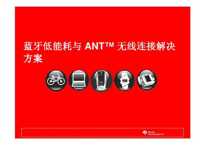
蓝牙低能耗与 ANT™ 无线连接解决 方案TI 推出蓝牙低功耗与 ANT™ 技术TI 推出业界首款完整型蓝牙 (Bluetooth®) 低能耗解决方案与最高集成型 ANT™ 网络处理器,进一步扩展在无线连接领域 的领先地位。
面向消费类医疗、移动附件、运动以及保 健应用的超低功耗短距无线技术。
CC2540 单模式蓝牙低能耗片上系统与 CC257x ANT™ 网络处理器 (CC257x) 可使目标应用通过一颗纽扣电池连续工作超过 1 年。
加上 WiLink6.0 及 7.0,TI 可为传感器应用与移动手持外设提供全面测 试的高稳健型产业环境。
短距离无线通信距离专有低功耗无线电1000m游戏 计算机外设 音频 抄表 楼宇管理 汽车100mZigBee PRO / RF4CE楼宇自动化 智能能源/ 智能能源/电表 RC/消费类电子 / 医疗 PAN 电信10m耳机 计算机外设 PDA/移动电话 /Wi-Fi/802.11PC 网络 家庭网络 视频分配1m 10cm 1k低能耗 移动电话配件 游戏/ 游戏/HID/遥控 / 运动、医疗、 运动、医疗、消费类保健产品UWB无线 USB 视频/ 视频/音频链路RFid NFC数据数率 (bps)10k100k1M10MCC2540 蓝牙低能耗片上系统什么是蓝牙低能耗? 什么是蓝牙低能耗?• 先前的蓝牙低功耗 (ULP) 与 Wibree充分利用现有的蓝牙产业环境 支持 BL/BLE 的双模式几乎被用于所有的手机/PC•目标应用为低成本的低功耗短距离 RF 连接– 传感器/执行器可通过纽扣电池运行数月/数年 – 低带宽设备可进行定期或无规律传输•主要目标市场– – – – 手机附件 运动/休闲/医疗设备 游戏/HID/遥控 “近距离“应用 — 安全或者其它空间感测应用• •CC2540 是 TI 单模式器件解决方案:支持蓝牙低能功耗技术 在蓝牙 4.0 中发布的 BLE 已于 2010 年 7 月投入使用蓝牙低能耗应用运动传感器来电显 示、警 报CC2540Single-mode Bluetooth LE dongleUSB 接口可解决短距离 PC 接口连接问题短距离标签、 密钥卡等CC2540 蓝牙低能耗 SoC• • • • •单芯片器件• • • • •6 毫米 x 6 毫米封装中的集成型控制器、主机与应用可 缩小物理尺寸,降低成本。
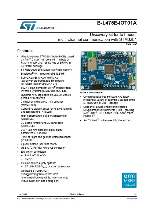
For further information contact your local STMicroelectronics sales office.July 2018DB3143 Rev 41/4B-L475E-IOT01ADiscovery kit for IoT node,multi-channel communication with STM32L4Data briefFeatures•Ultra-low-power STM32L4 Series MCUs based on Arm ® Cortex ®-M4 core with 1Mbyte of Flash memory and 128Kbytes of SRAM, in LQFP100 package •64-Mbit Quad-SPI (Macronix) Flash memory •Bluetooth ® V4.1 module (SPBTLE-RF)•Sub-GHz (868MHz or 915MHz)low-power-programmable RF module (SPSGRF-868 or SPSGRF-915)•802.11 b/g/n compliant Wi-Fi ® module from Inventek Systems (ISM43362-M3G-L44)•Dynamic NFC tag based on M24SR with its printed NFC antenna • 2 digital omnidirectional microphones (MP34DT01)•Capacitive digital sensor for relative humidity and temperature (HTS221)•High-performance 3-axis magnetometer (LIS3MDL)•3D accelerometer and 3D gyroscope (LSM6DSL)•260-1260hPa absolute digital output barometer (LPS22HB)•Time-of-Flight and gesture-detection sensor (VL53L0X)• 2 push-buttons (user and reset)•USB OTG FS with Micro-AB connector •Expansion connectors:–Arduino™ Uno V3–PMOD•Flexible power-supply options:–ST LINK USB V BUS or external sources •On-board ST-LINK/V2-1debugger/programmer with USBre-enumeration capability: mass storage, Virtual COM port and debug portPicture is not contractual.•Comprehensive free software HAL libraryincluding a variety of examples, as part of the STM32Cube M C U Package •Support of a wide choice of IntegratedDevelopment Environments (IDEs) including IAR ™, Keil ®, GCC-based IDEs, Arm ® Mbed Enabled ™•Arm ® Mbed ™online (see )Description B-L475E-IOT01A DescriptionThe B-L475E-IOT01A Discovery kit for IoT node allows users to develop applications withdirect connection to cloud servers.The Discovery kit enables a wide diversity of applications by exploiting low-powercommunication, multiway sensing and Arm® Cortex® -M4 core-based STM32L4 Seriesfeatures.The support for Arduino Uno V3 and PMOD connectivity provides unlimited expansioncapabilities with a large choice of specialized add-on boards.System requirements•Windows® OS (XP, 7, 8 and 10), Linux® or macOS®(a)•USB Type-A to Micro-B cableDevelopment toolchains•Keil® MDK-ARM(b)•IAR™ EWARM(b)•GCC-based IDEs including free SW4STM32 from AC6•Arm®(c) Mbed Enabled™ onlineDemonstration softwareThe demonstration software is preloaded in the STM32L475VG Flash memory for easydemonstration of the device peripherals in standalone mode. The latest versions of thedemonstration source code and associated documentation can be downloaded from the/x-cube-cloud webpage.a.macOS® is a trademark of Apple Inc., registered in the U.S. and other countries.b.On Windows® only.c.Arm and Mbed are registered trademarks or trademarks of Arm Limited (or its subsidiaries) in the US and orelsewhere.2/4DB3143 Rev 4DB3143 Rev 43/4B-L475E-IOT01A Laser considerationLaser considerationThe VL53L0X contains a laser emitter and corresponding drive circuitry. The laser output is designed to remain within Class 1 laser safety limits under all reasonably foreseeableconditions including single faults, in compliance with IEC 60825-1:2014 (third edition). The laser output will remain within Class 1 limits as long as STMicroelectronics recommended device settings are used and the operating conditions, specified in the STM32L4 Series datasheets, are respected. The laser output power must not be increased by any means and no optics should be used with the intention of focusing the laser beam. Figure 1 showsthe warning label for Class 1 laser products.Figure 1. Label for Class 1 laser productsOrdering informationTo order the B-L475E-IOT01A Discovery kit for IoT node, depending on the frequency of the Sub-GHz module, refer to Table 1.Revision historyTable 1. Ordering informationOrder code Sub-GHz operating frequencyB-L475E-IOT01A1915MHz B-L475E-IOT01A2868MHzTable 2. Document revision historyDate RevisionChanges02-Feb-20171Initial version.27-Mar-20172Updated Features and Description to add the PMOD connector.24-Apr-20173Added Section : Laser consideration to add Class 1 laser information.11-Jul-20184Updated the description of the Wi-Fi ® module in Features .B-L475E-IOT01AIMPORTANT NOTICE – PLEASE READ CAREFULLYSTMicroelectronics NV and its subsidiaries (“ST”) reserve the right to make changes, corrections, enhancements, modifications, and improvements to ST products and/or to this document at any time without notice. Purchasers should obtain the latest relevant information on ST products before placing orders. ST products are sold pursuant to ST’s terms and conditions of sale in place at the time of order acknowledgement.Purchasers are solely responsible for the choice, selection, and use of ST products and ST assumes no liability for application assistance or the design of Purchasers’ products.No license, express or implied, to any intellectual property right is granted by ST herein.Resale of ST products with provisions different from the information set forth herein shall void any warranty granted by ST for such product. ST and the ST logo are trademarks of ST. All other product or service names are the property of their respective owners.Information in this document supersedes and replaces information previously supplied in any prior versions of this document.© 2018 STMicroelectronics – All rights reserved4/4DB3143 Rev 4。
低功耗蓝牙方案引言低功耗蓝牙(Low Energy Bluetooth,简称LE Bluetooth或BLE)是一种蓝牙技术的子集,专门设计用于对功耗敏感的设备。
它的主要目标是减少能源消耗,增强设备寿命,同时保持与传统蓝牙技术兼容。
低功耗蓝牙方案在智能家居、健身追踪器、医疗设备、智能手表等领域得到广泛应用。
本文将介绍低功耗蓝牙方案的原理、特点以及在不同领域中的应用。
低功耗蓝牙方案原理低功耗蓝牙方案的核心原理是通过最小化功耗来延长设备的电池寿命。
以下是低功耗蓝牙方案的几个关键特点:1.快速连接和断开:低功耗蓝牙设备能够快速建立连接以及在完成任务后迅速断开连接,从而最大程度地减少功耗。
2.低工作周期:低功耗蓝牙设备可以在时间上进行均衡,仅使用短暂的时间段进行通信,其余时间处于睡眠状态。
这种方式可以大大降低功耗。
3.传输速率调整:低功耗蓝牙设备可以根据实际需求调整传输速率,以提供最佳的性能和能耗平衡。
特点及优势低功耗蓝牙方案相对于传统蓝牙技术具有以下特点和优势:1.减少电池消耗:低功耗蓝牙设备可以实现更低的功耗,延长电池寿命,节约能源,并减少对电池的更换频率。
2.小型化设计:低功耗蓝牙芯片体积小,适用于嵌入式系统和小型设备。
这使得低功耗蓝牙在可穿戴设备和物联网应用中具有广泛的适用性。
3.简化连接过程:低功耗蓝牙方案支持快速连接和断开,减少了用户的操作步骤,提升了使用体验。
4.低成本:低功耗蓝牙技术使用的芯片成本相对较低,这使得在大规模部署和推广低功耗蓝牙设备时更具优势。
5.兼容性:低功耗蓝牙技术与传统蓝牙技术兼容,这意味着低功耗蓝牙设备可以与传统蓝牙设备进行通信。
应用领域低功耗蓝牙技术在多个领域得到广泛应用,以下是一些典型的应用案例:智能家居低功耗蓝牙可用于智能家居应用,如智能门锁、智能插座、智能灯具等。
通过低功耗蓝牙连接设备,用户可以方便地使用手机或智能音箱等控制设备,实现智能家居互联互通。
健身追踪器低功耗蓝牙技术在健身追踪器中得到广泛应用。
低功耗蓝牙方案摘要:低功耗蓝牙(Low Energy Bluetooth,LE Bluetooth)是一种电力效率极高且对电池寿命要求较低的通信技术。
本文将探讨低功耗蓝牙的原理、应用场景以及其优势和不足之处。
引言随着物联网的快速发展,对于低功耗无线通信技术的需求也日益增长。
低功耗蓝牙作为一种新兴的通信标准,被广泛应用于智能家居、健康监测、智能穿戴设备等领域。
本文将详细介绍低功耗蓝牙的原理、应用以及其优势和不足之处。
一、低功耗蓝牙的原理低功耗蓝牙是通过频率跳变技术实现低功耗通信的。
传统蓝牙使用固定频率进行通信,而低功耗蓝牙使用的是频率跳变技术,即以固定的时间间隔在不同的频道之间快速切换。
这种频率跳变的方式可以减少信号干扰,提高通信质量,并且能有效降低功耗。
二、低功耗蓝牙的应用场景1. 智能家居:低功耗蓝牙可以连接各种智能设备,如智能灯泡、智能插座、智能门锁等,实现远程控制和智能化管理。
2. 健康监测:低功耗蓝牙可以连接健康监测设备,如心率监测器、血压计等,将实时数据传输到智能手机或其他设备上进行监测和分析。
3. 智能穿戴设备:低功耗蓝牙可以连接智能手表、智能眼镜等穿戴设备,实现与智能手机的互联互通,提供更多的功能和服务。
4. 物流管理:低功耗蓝牙可以用于物流管理中的货物追踪和定位,提高物流效率和减少人力成本。
5. 智能交通:低功耗蓝牙可以应用于智能交通领域,实现车辆之间的通信和信息交换,提高交通安全和交通效率。
三、低功耗蓝牙的优势1. 低功耗:相对于传统蓝牙,低功耗蓝牙的功耗更低,可以有效延长设备的电池使用时间。
2. 简单易用:低功耗蓝牙的连接和配置过程相对简单,用户可以快速便捷地完成设备的连接和操作。
3. 稳定可靠:低功耗蓝牙采用频率跳变技术,可以有效避免信号干扰,提高通信质量和稳定性。
4. 成本低廉:低功耗蓝牙的芯片价格相对较低,制造商可以降低产品成本,提高竞争力。
四、低功耗蓝牙的不足之处1. 传输距离有限:低功耗蓝牙的传输距离一般在10米左右,相对于传统蓝牙而言较短。
蓝牙最新版的推出引发话题,不仅适用於最新的穿戴式科技与健身装置,亦可在物联网(IoT) 中连接设备与感测器。
蓝牙4.0 大幅增进功率效率、简化直接蓝牙连结的使用,而且 4.1 规格更增加众多连线能力。
因此能为标准智慧型手机开启可能性,同时连接多重装置。
Bluetooth Smart 4.0 使用一颗电池即可让嵌入式连结运作数年,因此从2010 年起就持续受到采用,而且其内建的网路元件在2013 年12 月通过4.1 版认可,因此对IoT 开发人员而言更具吸引力。
即便如此,在硬体和软体层面的设计上仍然需要一些重大考量。
SIG 建议制造商开始在装置上采用蓝牙 4.1,立即享受新功能的优势。
这也确定系统开发商可继续沿用供应商(如Laird Wireless、BlueGiga Technologies、Panasonic 和ConnectBlue 等)既有的4.0 模组,然後在韧体稳定时升级至 4.1,因此同时享有两大优势。
自从蓝牙2.0 + EDR 开始采用以来,蓝牙 4.1 是首次未对必备功能设限的规格。
然而,制造商必须在蓝牙 4.1 上采用勘误表,才可符合规格。
仅采用低功耗功能的装置(Bluetooth Smart 品牌)将可向下相容於蓝牙4.0 装置(亦采用低功耗功能)。
低功耗蓝牙4.0 版(现称Bluetooth Smart)采用与之前「Classic Bluetooth」相同的 2.4 GHz ISM 频带频率,但运用更简易的高斯频移协定降低功耗。
也采用更小的2 MHz 通道以及直接序列展频(DSSS) 调变。
由於结合不同的通道与调变机制,因此LE 和Classic 规格彼此无法直接相容。
但对开发人员来说,这不会构成问题,所有通过蓝牙相容认证的晶片与模组皆可采其中一种模式运作,旧款装置运行Classic,DSSS 款式则运行Bluetooth Smart。
4.0 和4.1 版采用40 个2 MHz 通道,达到低功率优势,能让连结达到1 Mbit/s 位元率以及270 kbit/s 的应用传输率。
使用新的认证模块,轻松向现有的MCU添加低功耗蓝牙通过蓝牙®4.2将产品连接到智能手机,这样就提供了两个明显的优势,便于许多应用进行利用:丰富的用户界面(手机之外的大多数电子产品没有大型高分辨率触摸屏)低功耗接近检测和固有云连接(智能手机通常具有互联网连接)借助TI的新SimpleLink™低功耗蓝牙CC2650MODA模块,您的产品可以极其轻松地实现这些优势。
预认证的CC2650MODA模块(有关预认证的完整列表,请参见数据表)包含配备15个通用IO(GPIO)引脚和集成天线的SimpleLink CC2650无线微控制器(MCU)。
使用来自TI BLE-Stack 2.2软件开发工具包(SDK)的不同固件配置,TI的这款新模块可以作为控制系统中所有内容的独立片上系统(SoC)或作为无线网络处理器让您向任何现有的MCU添加低功耗蓝牙连接。
在无线网络处理器配置中:低功耗蓝牙协议栈的主机和控制器组件在CC2650模块设备上运行,这与SimpleLink低功耗蓝牙CC2640无线MCU的引脚和代码兼容。
在MSP432™ MCU等主机MCU上运行的应用程序和相关的蓝牙服务和配置文件。
无论在独立还是网络处理器工作模式下使用该模块,您都将受益于CC2650MODA 模块更好的6-10dB链路预算,微小的放大器待机电流以及改进的RF传输范围。
TI创建了简单网络处理器(SNP)固件配置,使系统设计人员能够在主要用于与智能手机进行数据交换的主机MCU上快速编写服务级低功耗蓝牙应用。
这是通过在使用UART接口连接模块的主机MCU上集成轻量级API库来实现的。
管理与智能手机的连接等低功耗蓝牙功能由模块上的SNP固件利用与主机处理器交换的用户数据来处理。
在使用现有应用MCU运行简单网络处理器配置时,使用CC2650MODA模块有几项明显的优势:系统分区:用CC2650MODA模块负责所有低功耗蓝牙相关活动,而主机MCU可以专注于运行系统应用。
如何利用蓝牙4.1为物联网构建低功耗无线链路不仅在最新的可穿戴和健身设备方面,而且在将物联网(IoT)中的设备与传感器互连方面,最新蓝牙技术都带来不小的震动。
在提升蓝牙直接链路的电源能效、简化其使用方面,蓝牙4.0 实现了大跨越,而蓝牙4.1 则为该链路增加了更多的组网能力。
这使得用一部标准智能手机将许多设备连接在一起成为可能。
凭一块电池就能让嵌入式链路运行数年,这一功能自2010 年以来一直推动者智能蓝牙4.0 的普及,而组网能力又使该功能在蓝牙4.1 于2013 年批准以来对IoT 开发人员更具吸引力。
不过,这需要在设计过程中了解软硬件方面的一些关键注意事项。
SIG 建议制造商在产品中立即采用蓝牙4.1,以充分利用新特性。
这样,系统开发人员就会放心地采用由Laird Wireless、BlueGiga Technologies、Panasonic 和ConnectBlue 等制造商提供的现有4.0 模块,并在固件稳定时升级至4.1 版,实现鱼和熊掌兼得。
使用蓝牙4.1 规范时,已没有必要发布强制性特性声明,这在蓝牙2.0 + EDR 被采用以来还属首次。
但是,需要制造商们执行有关蓝牙4.1 的全部勘误,从而符合该规范要求。
仅具有低功耗特性的设备(智能蓝牙品牌)会向后兼容同样具有低功耗特性的蓝牙4.0 设备。
低功耗蓝牙(4.0 版,也称作智能蓝牙)采用与前代传统蓝牙相同的2.4GHz ISM 频带,但采用了更简单的高斯频移协议来降低功耗。
此外,还采用了较小的2 MHz 信道和直接序列扩频(DSSS)调制功能。
这种不同信道和不同调制功能的组合意味着无法直接兼容LE 和传统规范。
然而,这对开发人员来说不是问题,因为获得蓝牙兼容性认证的所有芯片和模块都能在适用于旧设备的传统蓝牙模式或具有DSSS 功能的智能蓝牙模式。
基于蓝牙低功耗的4.1mcu解决方案篇一:Atmel ATBTLC1000超低功耗蓝牙SMART (BLE )解决方案Atmel ATBTLC1000超低功耗蓝牙SMART (BLE 4.1)解决方案Atmel公司的ATBTLC1000是超低功耗蓝牙SMART (BLE )系统级芯片(SoC),集成了ARM? Cortex?-M032位MCU,收发器,调制解调器,MAC,PA,TR开关和功率管理单元(PMIC),可用作蓝牙低功耗连接控制器或数据泵,或嵌入了BLE连接和外接存储器的单独应用处理器,主要用在医疗电子如血氧仪,心率仪,血压计,体温计等.本文介绍了ATBTLC1000主要特性,框图,以及ATBTLC1000-MR110CA模块框图,电路图和材料清单以及BTLC1000 Xplained Pro扩展评估板主要特性.The Atmel? ATBTLC1000 is an ultra-low power Bluetooth? SMART (BLE ) System on a Chip with Integrated MCU, Transceiver, Modem, MAC, PA, TR Switch, and Power Management Unit (PMU). It can be used as a Bluetooth Low Energy link controller or data pump with external host MCU or as a standalone applications processor with embedded BLE connectivity and external memory.The qualified Bluetooth Smart protocol stack isstored in ded(来自: 小龙文档网:基于蓝牙低功耗的解决方案)icated ROM. The firmware includes L2CAP service layer protocols, Security Manager, Attribute protocol (ATT), Generic Attribute Profile (GATT), and the Generic Access Profile (GAP). Additionally, application profiles such as Proximity, Thermometer, Heart Rate, Blood Pressure, and many others are supported and included in the protocol stack.ATBTLC1000主要特性:Complies with Bluetooth , ETSI EN 300 328 and EN 300 440 Class 2, FCC CFR47 Part 15 and ARIB STD-T66?transceiver and modem?–-95dBm/-93dBm programmable receiver sensitivity– -20 to + programmable TX output power– Integrated T/R switch– Single wire antenna connectionARM? Cortex?-M0 32-bit processor?– Single wire Debug (SWD) interface– Four-channel DMA controller– Brownout detector and Power On Reset– Watch Dog TimerMemory?–128kB embedded RAM (96kB available for application)– 128kB embedded ROMHardware Security Accelerators?– AES-128– SHA-256Peripherals?– 10 digital and one wakeup GPIOs with 96kΩinternal pull-up resistors, one Mixed Signal GPIO – 2x SPI Master/Slave– 2x I2C Master/Slave and 1x I2C Slave– 2x UART– 1x SPI Flash– Three-Axis quadrature decoder– 4x Pulse Width Modulation (PWM), three General Purpose Timers, and one Wakeup Timer– 1-channel 11-bit ADCClock?– Integrated 26MHz RC oscillator– 26MHz crystal oscillator– Integrated 2MHz sleep RC oscillator– RTC crystal oscillatorUltra Low power?–μA sleep current (8KB RAM retention and RTC running)– peak TX current (0dBm, )– peak RX current (, -93dBm sensitivity)–μA average advertisement current (three channels, 1s interval)Integrated Power management?– to battery voltage range– Fully integrated Buck DC/DC converterBluetooth SIG Certification?– QD ID Controller (see declaration D028678)– QD ID Host (see declaration D028679)图框图图电源架构图图模块框图图模块电路图ATBTLC1000-MR110CA模块材料清单:BTLC1000 Xplained Pro扩展评估板The Atmel? BTLC1000 Xplained Pro extension evaluation kit is to evaluate the Atmel? ATBTLC1000-MR110CA BLE module. The BTLC1000 MR110CA module is based on Atmel’s industry – leading lowest power Bluetooth Low Energy compliant SoC, ATBLTC1000-MU-T. The XPro extension can be plugged into any of the supported Atmel’s host MCU Xplained Pro evaluation boards to quickly add Bluetooth Smart connectivity to the existing host MCU platform. Supported by the Atmel Studio integrated development platform, the kit provides easy access to the features of the Atmel’s篇二:超低功耗蓝牙协议规范解析[摘要]:本文介绍了一种功耗比标准蓝牙更低的超低功耗蓝牙技术,分别描述了这种技术的由来、协议栈构成、拓扑结构、Radio层的工作状态和工作角色以及特点。
在技术特点部分中,详细介绍了超低功耗蓝牙技术实现低功耗的原理。
[关键词]:超低功耗;蓝牙;跳频;低能耗[Abstract]:This article introduces a technology of Ultra Low Power Bluetooth whose power is lower than the standard Bluetooth, describes respectively origin,structure of protocol stack and topology, operating states and roles of Radio layer, characteristics of the technology. In the part of characteristics of the technology, the reason why Ultra Low Power Bluetooth technology can realize ultra low power is detailed, and a table that contains some parameters of Ultra Low Power Bluetooth compared with the standard Bluetooth technology is also showed.[Keywords]:ultra low power; Bluetooth; frequency hopping; low energy目录第1章蓝牙技术简介 (1)蓝牙技术的概述 (1)蓝牙技术的特点 ................................2蓝牙技术的应用 ................................5ULP蓝牙技术的价值 ...........................8第2章ULP蓝牙系统体系结构 (10)ULP蓝牙系统体系结构概述 .....................10蓝牙系统的拓扑结构 ...........................11蓝牙系统RADIO层的状态和角色 .................13第3章ULP蓝牙技术规范 (15)物理层规范...................................15信道分配 (15)发射机 (15)接收机 (16)链路层规范...................................17主机接口规范.................................19主机规范.....................................22安全服务规范.................................26密钥 .......................................26匹配和密钥交换 (27)第四章蓝牙应用前景 (30)ULP蓝牙技术的特点 ...........................30ULP蓝牙技术的应用 ...........................34 致谢 ............................. 错误!未定义书签。