3W高精度恒流led照明驱动芯片SM7513
- 格式:pdf
- 大小:3.36 MB
- 文档页数:7
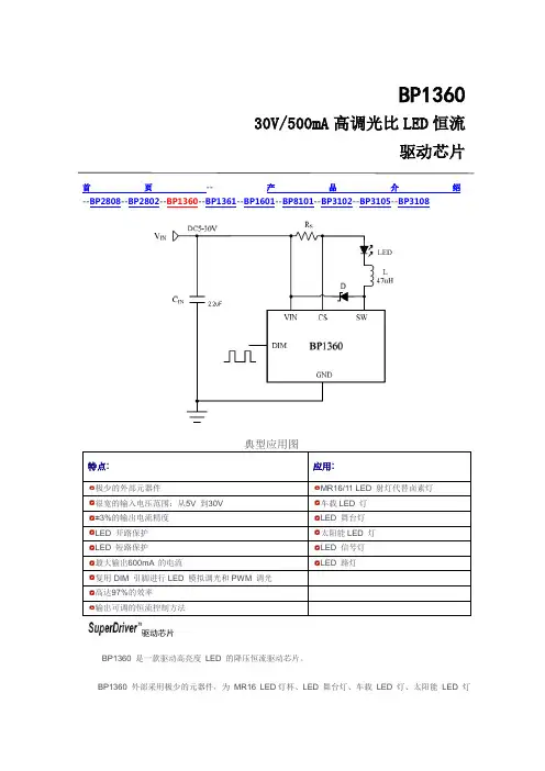
BP136030V/500mA高调光比LED恒流驱动芯片首页--产品介绍BP3108--BP2808--BP2802--BP1360--BP1361--BP1601--BP8101--BP3102--BP3105--特点:应用:极少的外部元器件MR16/11 LED 射灯代替卤素灯很宽的输入电压范围:从5V 到30V 车载LED 灯±3%的输出电流精度LED 舞台灯LED 开路保护太阳能LED 灯LED 短路保护LED 信号灯最大输出600mA的电流LED 路灯复用DIM 引脚进行LED 模拟调光和PWM 调光高达97%的效率输出可调的恒流控制方法驱动芯片BP1360 是一款驱动高亮度LED 的降压恒流驱动芯片。
BP1360 外部采用极少的元器件,为MR16 LED灯杯、LED 舞台灯、车载LED 灯、太阳能LED 灯和LED 路灯提供一个极高性价比的解决方案。
BP1360输入电压范围从 5 伏到30 伏,输出电流通过采样电阻设定,单颗LED 最大输出电流可达600 毫安。
BP1360 采用专利技术的恒流控制方法使得LED 电流精度高达±3%。
BP1360 通过DIM 引脚接受0.5-2.5V 的模拟调光以及频率范围很宽的PWM 调光。
当DIM 的电压低于0.3V 时,功率开关关断,BP1360 进入极低工作电流的待机状态。
BP1360 内置功率开关,根据不同的输入电压,BP1360 可以驱动多颗1 瓦或单颗3 瓦的LED。
BP1360 包含过温保护、LED 短路和开路保护功能。
BP1360 采用体积很小SOT23-5 封装。
管脚封装管脚描述管脚号管脚名称描述1 SW 功率开关的漏端2 GND 信号和功率地3 DIM 开关使能、模拟和PWM调光端4 CS 电流采样端,采样电阻接在CS和VIN端之间5 VIN 电源输入端,必须就近接旁路电容定购信息定购型号封装温度范围包装形式打印BP1360ES5 SOT23-5 -40 o C到85 o C Tape and Reel 1360。
xx135 **** ****
公司专业的角度为您提供优质的产品,让您用实惠的价格,购买到您需要的产品和优质的服务。
升压芯片,同步降压芯片,同步升压降压芯片,LED背光驱动IC,LED照明驱动IC,线性恒流IC,线性稳压LDO,锂电充电IC,锂电保护IC,电压检测IC等等是我们的主打产品。
同时我们提供专业的技术支持,让您能更快的设计生产产品,获得市场先机。
LED手电筒驱动专用IC特点:
工作电压:2V~6V
工作模式1:全亮、闪亮
工作模式2:全亮、暗亮、闪亮
最大LED电流:200mA
欠压保护:2V
LED手电筒驱动专用IC应用领域:
LED手电筒装
LY2210采用SOT23和TO92两种封装
LED矿灯、头灯
专门为LED手电筒、矿灯、头灯等设计的控制芯片。
LY2210支持一组LED 灯,灯的控制由开关来完成。
LY2210有两种工作模式:
在工作模式1下,LED灯可在"全亮"和"闪亮"这两种工作状态之间切换;在工作模式2下,LED灯可从"全亮"状态切换到亮度的"暗亮"状态再到"闪亮"状态,这三种工作状态是循环往复切换的。
LY2210最大工作电流为200m
A.
1/ 1。
简单介绍
AMC7135350mA恒流LED驱动ic方案汇总主要包含:1.基本典型应用。
2.防反接LED手电筒电路。
3.多颗AMC7135并联驱动700mA~1A应用。
4.高电压输入驱动多颗串接LED应用。
5.通过微控制器控制RGB 三色LED灯。
6.AMC7135主辅灯可切换的LED矿灯应用。
7.AMC713512V输入驱动三串多并LED应用。
AMC7135350mA恒流LED驱动ic方案汇总
概述AMC7135堪称一款经典的降压恒流驱动芯片。
平实的价格、简单的电路结构及稳定
的性能着实让它的使用者们津津乐道。
但是除了典型应用AMC7135还可以做更多的
事,简单的东西不简单就看大家怎么去发挥它了。
技术参数
350mA恒流输出(电流档位可选)
输出开短路保护
低压差
低静态电流
供电范围:2.7V~6V
2KV ESD
先进Bi-CMOS工艺
SOT89和TO252封装
AMC7135应用方案汇总见下(附电路图)
1.典型应用电路无需任何外围器件
2.防电池反接的LED驱动电路
3.多颗AMC7135并接驱动700mA~1A应用
4.输入12V驱动3颗串接白光LED应用(如负载改为红光LED VF=2V,该应用则可串5颗LED)
5.通过微控制器及on/off装置配合7135实现RGB三色LED亮暗程度的控制。
达到多彩混色的功
能。
6.矿灯所需的主灯及辅灯可切换照明电路
7.输入电压12V,采用78L05降压,配合7135实现1W LED3串多并电路
资料收集:冯教授。
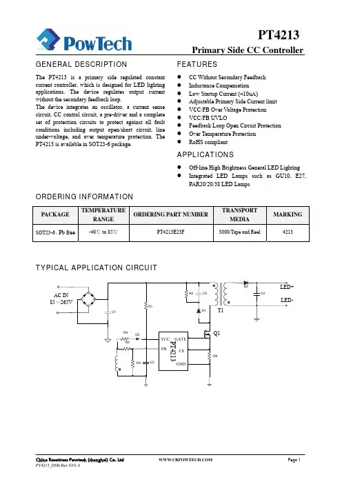
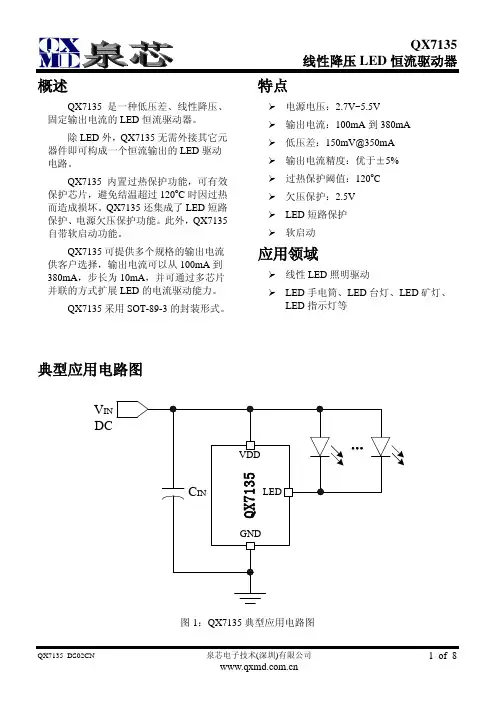
PT4213Primary Side CC ControllerGENERAL DESCRIPTIONThe PT4213 is a primary side regulated constant current controller, which is designed for LED lighting applications. The device regulates output current without the secondary feedback loop. The device integrates an oscillator, a current sense circuit, CC control circuit, a pre-driver and a complete set of protection circuits to protect against all fault conditions including output open/short circuit, line under-voltage, and over temperature protection. The PT4213 is available in SOT23-6 package.FEATURESCC Without Secondary Feedback Inductance Compensation Low Startup Current (<10uA) Adjustable Primary Side Current limit VCC/FB Over Voltage Protection VCC/FB UVLO Feedback Loop Open Circuit Protection Over Temperature Protection RoHS compliantAPPLICATIONSOff-line High Brightness General LED Lighting Integrated LED Lamps such as GU10, E27, PAR20/20/38 LED LampsORDERING INFORMATIONPACKAGESOT23-6, free PbTEMPERATURE RANGE-40℃ to 85℃ORDERING PART NUMBERPT4213E23FTRANSPORT MEDIA3000/Tape and ReelMARKING4213TYPICAL APPLICATION CIRCUITD2LED+C4AC IN 85~265VC1R2C2LEDR1 D1T1R5 R3D3Q1VCC FB GATE CSR6PT4213R4C3GNDChina Resources Powtech (shanghai) Co. LtdPT4213_DSB Rev EN1.0Page 1PT4213Primary Side CC ControllerPIN ASSIGNMENTPIN DESCRIPTIONSPIN No. 1 2 3 4 5 6 PIN NAMES CS GND NC GATE VCC FB DESCRIPTION Primary Side Current Sense Input Ground Not connected Drive output Power supply, the device is supplied by an auxiliary winding. Auxiliary Winding Voltage Sense InputABSOLUTE MAXIMUM RATINGS (note1)SYM PARAMETER VALUE UNITVCC VFB VCS VGATE Topt Tstg ESDRΘJAVCC pin Voltage FB pin Input Voltage CS pin Voltage GATE pin output voltage Operating Junction Temp. Range Storage Temp. Range HBMSOT23-6-0.3~30 -0.3~5 -0.3~5 -0.3~15 -40 to 150 -55 to 150 2000250V V V V ℃ ℃ V℃/WNote 1: Absolute Maximum Ratings indicate limits beyond which damage to the device may occur. Recommended Operating Range indicates conditions for which the device is functional, but do not guarantee specific performance limits. Electrical Characteristics state DC and AC electrical specifications under particular test conditions which guarantee specific performance limits. This assumes that the device is within the Operating Range. Specifications are not guaranteed for parameters where no limit is given, however, the typical value is a good indication of device performance.RECOMMENDED OPERATING RANGESYM PARAMETER VALUE UNITVCC TAVCC pin Operating Voltage Operating Ambient Temperature9.5~26 -20~85V ℃China Resources Powtech (shanghai) Co. LtdPT4213_DSB Rev EN1.0Page 2PT4213Primary Side CC ControllerELECTRICAL CHARACTERISTICS(TA=25℃, VCC=16V,fsw=65KHz unless specified otherwise) SYMBOL PARAMETER TEST CONDITION MIN TYP MAX UNITSUPPLY VOLTAGE (VCC) ISTART VVCC_ON VVCC_OFF VVCC_Clamp VVCC_OVP IVCCQ Start up current VCC turn on threshold VCC minimum voltage operating VCC=12.0V VCC Rising VCC Falling Icc=10mA 26 No switching 12.5 7.5 1 14.0 8.5 33 27.5 350 29 700 10 15.5 9.5 uA V V V V uAVCC Clamp Voltage VCC Over Voltage Protection Threshold VCC Supply CurrentFEED BACK VOLTAGE SENSE PIN (FB) VFBMAX VFBMIN IFB_OPEN FB Over Voltage Protection FB Minimum Voltage FB Open Loop Current 2.4 2.5 0.8 -85 2.6 V V uACURRENT SENSE INPUT PIN (CS) VCS TLEB Current Limit Threshold Current sense Leading Edge Blanking Time Maximum driving pulse duty cycle Rising time Falling time Gate clamp voltage Cgate=1nF Cgate=1nF Ifb=0 490 500 250 510 mV nSDRIVE OUTPUT (GATE) Dmax Tr Tf VGS_MAX PROTECTION TSD Thermal Threshold Shut Down 150 ℃ 65 220 120 15 % nS nS VChina Resources Powtech (shanghai) Co. LtdPT4213_DSB Rev EN1.0Page 3PT4213Primary Side CC ControllerSIMPLIFIED BLOCK DIAGRAMOPERATION DESCRIPTION The PT4213 consists of an oscillator, feedback circuit, over-temperature protection, frequency jittering, current limit circuit, leading-edge blanking, and constant current control circuitry. The switching frequency is modulated to regulate the output current to provide a constant current characteristic. It senses and regulates output current from primary side of transformer and is ideal for high precise, high reliability and cost effective LED lighting application. THEORY OF OPERATIONFigure 1 illustrates a simplified flyback converter. When the switch Q1 turns on, the voltage across the primary winding is Vbus. Assuming the voltage dropped across Q1 is zero, the current in Q1 ramps up linearly at a rate of Vbus/Lp. When the current in Q1 reaches a predefined value of Ipk_pri the controller forces Q1 turns off. During the Q1 on-time, the rectifying diode D2 is reverse biased and the load current Io is supplied by the secondary capacitor C4. When Q1 turns off, D2 conducts and the stored energy is delivered to the output. The PT4213 is designed to operate in discontinuous conduction mode (DCM), in DCM the energy stored in primary winding is transported to the secondary winding completely during each cycle. The output current is determined by Rcs and primary/secondary turns ratio of the transformer. Assuming the transformer primary/secondary turns ratio is Nps. The output current is given by following expression:China Resources Powtech (shanghai) Co. LtdPT4213_DSB Rev EN1.0Page 4PT4213Primary Side CC ControllerI out = 0.1125 * N ps Rcssource terminal and GND and feeds to CS input. At each switching cycle when the voltage of CS input excess the internal threshold the driving signal is terminated after a short delay. The relationship between the CS threshold and the primary peak current passing through power MOSFET Q1 follows below expression: Ipk_pri=Vcs/Rcs; Ipk_pri is the peak current through power MOSFET, VCS is the voltage threshold of pin1 of PT4213 and Rcs represents sensing resistor. A spike is inevitable on the sensed signal on Rcs at the instance when the power MOSFET is turned on due to the recovery time of the secondary rectifier and the snubber circuit. The LEB has been implemented in PT4213, during the LEB time the current sense comparator is disabled so the switching signal can not be terminated by the turn-on spike on the sensed signal so the external RC filter can be removed.START UP Once the AC voltage is applied to the application circuit, the Vbus charges VCC pin up through the start up resistor R1, when the voltage on VCC pin reaches its VCC_ON threshold the controller starts to deliver the driving pulses to power switch Q1 and VCC is powered by auxiliary winding. Thanks to the very small start up current, a large start up resistor R1 could be used in the start up circuit to minimize power loss. For the applications with general 90-264Vac input range, a 1/8W resistor between 0.5Mohm and 3Mohm and a 4.7uF/50V capacitor C3 compose a simple and reliable start up circuit.CURRENT LIMIT COMPENSATION CONSTANT CURRENT (CC) OPERATION The PT4213 regulates output current from the primary side control. The switching frequency is adjusted as the feedback pin voltage increases to provide a constant output current regulation. PRIMARY INDUCTANCE COMPENSATION With the inductance compensation function output current is free of primary inductance variation. If the primary magnetizing inductance is either too high or low the converter will automatically adjust the Oscillation frequency to maintain the constant output current. CURRENT SENSE AND LEB The current of the power MOSFET is transferred to voltage signal through a resistor connected between The current limit circuit senses the current in the power MOSFET from the resistor connecting between the source of MOSFET and GND. The current sense resistor converts the current in the power MOSFET to voltage signal and then feeds to CS pin. When the voltage on CS pin exceeds the internal threshold VCS which is defied as 500mV, the power MOSFET is turned off for the remainder of that cycle. Excellent regulation performance is achieved with C.R.PowTech proprietary line regulation control technique. SHORT CIRCUIT PROTECTION In the event of a fault condition such as an output short condition the PT4213 enters into an appropriate protection mode as described below. In the event the feedback pin voltage falls below 0.8V during theChina Resources Powtech (shanghai) Co. LtdPT4213_DSB Rev EN1.0Page 5PT4213Primary Side CC Controllerdischarged period of the inductance of the primary winding, the converter enters into short circuit protection mode after the feedback pin sampling delay for the duration in excess of ~30 ms, wherein the device is disabled. VCC will then drops due to internal power consumption. When VCC drops below the VVCC_OFF turn-off threshold, the PT4213 will be totally shut down and the start up sequence will kick in and VCC is charging up again. The device is alternately enables and disables until the fault condition is removed. OPEN CIRCUIT PROTECTION In the event of a fault condition of the output open circuit the PT4213 enters into an appropriate protection mode as described below. In the event the feedback pin voltage is over 2.5 V during the discharged period of the Lp (the inductance of the primary winding of the main transformer), the switching frequency is decreased and peak current is also decreased to 50%. If the over voltage condition duration time excess 8 consecutive cycles the controller is disabled. FREQUENCY JITTERING The frequency jittering is implemented in the PT4213. The oscillation frequency is modulated so that the tone energy is spread out. The spread spectrum minimizes the conduction band EMI and therefore reduces system design challenge. OVER TEMPERATURE PROTECTION The thermal shutdown circuitry senses the die temperature. When the die temperature is above 150°C the device is disabled and remains disable until the die temperature falls by 20°C. VCC OVER VOLTAGE PROTECTION VCC over voltage protection is designed to protect the device from damage of over voltage. When the voltage on VCC reaches the OVP threshold the PT4213 stops delivering PWM signal to the power MOSFET, voltage on VCC begins to drop due to the internal power consumption, the PT4213 will recover from OVP status when voltage on VCC drops below the OVP release threshold. GATE OUTPUT The output drives the GATE of the power MOSFET. The optimized totem-pole type driver offers a good tradeoff between driving ability and EMI. Additionally the output high level is clamped to 15V by an internal clamp so that power MOSFET transistor can be protected against undesirable gate over voltage. A resistor between GATE and GND initials the gate voltage to zero at the off state.China Resources Powtech (shanghai) Co. LtdPT4213_DSB Rev EN1.0Page 6PT4213Primary Side CC ControllerTYPICAL PERFORMANCE CHARACTERISTICSDESIGN Example and Notes: A design example is given to illustrate how to design an Off-line AC/DC LED driver step by step based on PT4213. Refer to figure 4 for the application circuit. 1 Determine input and output The design spec is given in Table 1. It is intended to drive 5pcs 1W white LED in series for general lighting Table 1 Parameters Input Voltage Symbol Vin Limits 90-264VacFrequency Output Voltage Max Vout Min Vout Output Currentfline Vout Voutmax Voutmin Iout47-64Hz 16V 17.5V 15V 320mA2 Set the switching frequency The maximum operating frequency is limited by PT4213 sampling delay time on FB pin during the flyback period. To sample the voltage on FB pin correctly the secondary side discharge duration timeChina Resources Powtech (shanghai) Co. LtdPT4213_DSB Rev EN1.0Page 7PT4213Primary Side CC Controllermust be more than 3.5uS, and the maximum limited switching frequency for PT4213 is 128 KHz. In practice, the suitable switching frequency for this design is set to 65KHz considering the EMI, efficiency and the size of the main transformer. For this design example, the switching frequency fsw and operating period Tsw is set as below: f sw = 65 KHz rectifying diode D3, the primary side inductance Lp, the primary peak current Ipk_pri, and the minimum operating input voltage Vin_dc_min. The smaller of Nps, the smaller of Vin_dc_min and less capacitance of the bulk capacitor is required. But it is led to higher reverse voltage for the secondary rectifying diode D3. In practice, the recommended Nps is less than 5.0 for general applications with 85VAC-265VAC input.Tsw = 1 / f sw = 15.4us3 The maximum duty cycle For PT4213, the discharged time tdis of the inductance of the primary winding is fixed to be 45% of the operating cycle. Keep in mind the operation of the LED driver using PT4213 should be DCM in the full input voltage range in order to regulate the LED current precisely. So: Tsw = ton + t dis + t dead ton: turn on time of the switch MOSFET Q1 tdis: discharge time of Lp tdead: dead time of the flyback DCM mode t dis = 0.45 * Tsw (2) (3) (1)Vin _ dc _ min * t on _ max = N ps * Vout * t disFrom equation (4), the below equation is given(4)N ps =Vin _ dc _ min * t on _ maxVout * t dis(5)For this design example, the minimum operating input voltage is estimated to be approximately 60Vdc as a start point.N ps =Vin _ dc _ min * t on _ maxVout * t dis= 60 * 5.3916 * 6.93= 2.925 Calculate the current sense resistor Once Nps is determined, the current sense resistor Rcs can be calculated from following expression:t dead _ min = 1.5 * 2π L p * CdsRcs =For this design example, the minimum tdead_min can be estimated to be approximately 20% of the switch cycle as a start point and then adjusted after the LED driver is made.0.1125 * N ps I out Vcs 0.5V = Rcs Rcs(6)I pk _ pri =(7)t dead _ min = 1.5 * 2π L p * Cds = 20% * Tsw = 3.08ust dis = 45% * Tsw = 6.93usFor this design example,R4 = Rcs =ton _ max = Tsw − t dis − t dead _ minDmax = ton _ max T sw = 35%0.1125 0.1125 * 2.92 = 1.0Ω * N ps = I out 0.32I pk _ pri =Vcs 0.5V 0.5V = = = 0.5 A Rcs Rcs 1.0Ω4 Turns Ratio The maximum allowable Nps is determined by the voltage stress on power switch Q1, the minimum operating voltage Vin_dc_min and primary side inductance Lp. The minimum allowable Nps is limited by the maximum allowable reverse voltage on the secondary rectifying diode D3. So the Nps is the trade-off among the Drain-Source breakdown voltage of the power switch Q1, the breakdown voltage of the secondary6 Calculate the primary inductance Primary inductance Lp is determined by the output power, the switch frequency fsw, the primary peak current Ipk_pri and the flyback converter efficiencyη . The relationship between primary energy and the secondary energy is given by:1 2 L p * I pk − pri * Fsw *η = Vout * I out 2(8)From the equation (8), the primary inductance Lp of theChina Resources Powtech (shanghai) Co. LtdPT4213_DSB Rev EN1.0Page 8PT4213Primary Side CC Controllermain transformer can be derived: 2 * Vout * I out Lp = 2 I pk − pri * Fsw *η and Rfb_dn (9) For better regulation the current flowing out from FB pin of PT4213 at 220VAC input voltage is better to be approximate 1mA, so the Rfb_up is given by:For this design example, 2 * Vout * I out 2 * 16 * 0.32 Lp ≤ = = 0.7 mH 2 0.52 * 65 * 103 * 0.90 I pk − pri * Fsw *η For this design example, Lp is chosen to be 660uH. 7 Calculate the primary winding In order to keep the transformer from saturation, the maximum flux density must not be exceeded. So the minimum turns of the primary winding must meet: L p * I pk _ Pr i (10) Np = Ae *ΔBmax Where ΔBmax is the maximum allowed flux density and Ae is the core effective area. For this design example, EE16 core is selected. From the EE16 transformer core datasheet, Ae is 19.2,R fb _ up =2 * 220V N a * Np 1mA(13)Rfb_up unit is KΩ . For this design example,2 * 220V 17 * = 76.6 KΩ 1mA 69 R5 is chosen to be 75 KΩ for R5 for this design The low side feedback resistor is selected to set the R5 = R fb _ up =output OVP. Rfb_dn should be selected so that when output voltage reaches OVP, the voltage on FB pin reaches VFBMAX during transformer reset time. The relationship between Vovp and VFBMAX is:ΔBmax is chosen to be 2500 Gauss. So:Np = L p * I pk _ pri Ae *ΔBmax = 0.66 * 10 −3 * 0.5 = 68.75 19.2 *10 −6 * 0.25V FBMAX =R fb _ dn R fb _ up + R fb _ dnNa (Vovp + Vd ) (14) NsRe-arrange above expression Rfb_dn can be derived as:69 turns is chosen for this deign example. 8 Calculate the secondary winding The turns of the secondary winding can be calculated:R fb _ dn =V FBMAX * R fb _ up Na Ns(Vovp+ V d ) − V FBMAX(15)Ns =Np N ps(11)Vd: forward voltage drop of the secondary side rectifier diode, VFBMAX is maximum FB pin operating voltage which has a typical value of 2.5V. For this design example,For this design example,Ns =Np N ps=69 = 23.63 2.92R6 = R fb _ dn =2.5 * 75 = 14.82 KΩ . 17 (20 + 0.5) − 2.5 2323 turns is chosen for this design example. 9 Calculate the auxiliary winding The turns of the auxiliary winding can be calculated:R6 is chosen to be 15 KΩ ; output OVP is set to be 20V for this design example. 11 Select the secondary and auxiliary rectifying diode Maximum reverse voltage on secondary and auxiliary rectifying diode is: (12)Na =Vcc * Ns VoutIn practice Vcc is set to be 12V. For this design example,Na =Vcc 12 * N s = * 23 = 17.25 Vout 16Vsec_ diode ≥ (2 * 265 * N s + Vout ) Np(15)17 turns is chosen for this design example. 10 Determine feedback resistors Rfb_upChina Resources Powtech (shanghai) Co. LtdPT4213_DSB Rev EN1.0Page 9PT4213Primary Side CC ControllerVaux _ diode ≥ ( 2 * 265 * N a + Vcc ) Npis filtered by the bulk capacitors C1 and C2. Inductor (16) L1, C1 and C2 form a pi (π) filter, which attenuates conducted differential-mode EMI noise. The secondary side of the transformer is rectified by D3, an ultra fast recovery diode and filtered by C5. The feedback resistors (R5 and R6) were selected using standard 1% resistor values for closed LED current. The feedback resistors should be placed directly at the FB pin of the PT4213 device to minimize noise. R1, R2 and C4 forms the start up circuit; the auxiliary winding is powered PT4213 through R7 and D2. C4 should be place as close as possible to the VCC and GND pins. R4 is the primary side current sense resistor, should be placed close to CS pin of PT4213.Peak current flowing in secondary rectifying diode is:I pk _ sec =0.5 * N ps Rcs(17)The secondary rectifying diode should be selected with the break down voltage higher than Vsec_diode and average forward current should be selected based on the output current and the secondary peak current. The auxiliary rectifying diode should be selected with the break down voltage higher than Vaux_diode. 12 PCB Layout The circuit shown in Figure 4 is configured as a primary-side regulated off-line flyback power supply utilizing PT4213 with 320mA CC output for driving 5pcs 1W LED in series. AC input power is rectified by BD1. The rectified DCChina Resources Powtech (shanghai) Co. LtdPT4213_DSB Rev EN1.0Page 10REFERENCE CIRCUIT FOR DRIVING 5X1W LEDFigure 4 PACKAGE INFORMATION (SOT23-6)尺寸(单位:毫米)尺寸(单位:英寸)符号最小值最大值最小值最大值A 0.787 1.450 0.031 0.057 A1 0.152 0.006B 1.397 1.803 0.055 0.071 b 0.250 0.559 0.010 0.022C 2.591 2.997 0.102 0.118D 2.692 3.099 0.106 0.122 e 0.838 1.041 0.033 0.041 H 0.080 0.254 0.003 0.010 L 0.300 0.610 0.012 0.024。

不知道发过没?各大LED驱动芯片大全Fairchild (美国飞兆) FSEZ 1016主要应用于3W灯杯3WFSEZ 1216主要应用于5W灯杯5WFSQ 110主要应用于8W左右LED电源8WFSDH 321主要应用于8W左右LED电源8WKA5M02659RN主要应用于12W左右LED电源12WKA5M0365R/KA5M0380RYDTU主要应用于30W左右LED电源30WFSDL0165/FSDM0265/FSDM0365 主要应用于12-18WLED电源12-18WKA5L0365RN/KA5M0365RN主要应用于24WLED电源25WSG6859 + 2N60/4N60主要应用于日光灯等外置式LED电源30W 以下SG6741 + 7N60C/7N60C主要应用于日光灯等外置式LED电源60W 以下FSFR2100主要应用于LED路灯和大功率LED电源200W待补充Power Integrations (PI) LNK603/613PG/DG主要应用于2.5W的LED灯杯2.5WLNK604/614PG/DG主要应用于3.5W的LED灯杯3.5WLNK605/615PG/DG主要应用于4.5W的LED灯杯4.5WLNK606/616PG/GG主要应用于5.5W的LED灯杯5.5WTNY274/275/276/277P/G主要应用于5-8W LED电源5-8WTNY278/279/280P/G主要应用于10-14W LED电源10-14W待补充Supertex (美国超科) AT9933专为汽车设计用高达70V功率驱动ICHV9921/22/2385 to 264V AC or DC input voltage of 20 to400V. 20/30/50mAHV9925Output Current to 50mA;Universal 85-264V AC Operation;Fixed OFF-Time BuckConverter;Internal 500V Power MOSFETHV9903Power efficiency of up to 85%;Drives up to 6 White LEDs;2.6V to 4.6VSupply;power stage can operate at 1.8V;Built-in Soft Start;DC and PWM DimmingControlHV9910高压大功率直驱LED恒流器件HV9911高压双向检测大功率直驱LED恒流ICHV9931高压双向检测大功率直驱LED恒流IC,可PWM灰度调节待补充National (美国国半) 针对带有双电流槽和与IC兼容亮度控制的白色LED和QLED显示器的高效升压器LM3402针对高功率LED驱动器、6V至42V输入电压范围的0.5A持续电流降压电路LM3402HV 针对高功率LED驱动器,6V至75V输入电压范围的0.5A持续电流降压电路LM3404针对高功率LED驱动器,6V至42V输入电压范围的1A持续电流降压电路LM3404HV 针对高功率LED驱动器、6V至75V输入电压范围的1.0A持续电流降压电路LM5022针对升压和SEPIC稳压器的60V低压侧控制器,允许控制外部MOSFET来为LED提供LM2735 520kHz/1.6MHz - 有效使用空间的升压和SEPIC DC-DC稳压器LM3405用于LED驱动器500kHz/1.6MHz 1A恒流降压稳压器LM2754具有超时保护功能的800mA开关电容Flash LED驱动器LM27965具有I2C兼容亮度控制功能的双显示器白光LED驱动器LM27966带有I2C兼容接口的白光LED驱动器LM2727/ LM2737 频道的FET 同步的为低输出电压顽强反抗调整者控制器待补充美国国家半导体公司白色LED低功率驱动部分LM3519高的频率推进白色LED用高速的PWM 光亮控制驱动ICLM2731SOT23 小封装小功率LED驱动应用SOT23 小封装5V升压到12-30V,120-300mALM26238-14V 转换成输出电压在1.24-14V之间,达到90% 的效率LM3557为白色LED2.7V-7.5V的递升转换器,多大5颗LED小体积背光指示LM35022.5-5.5V升压到16-44V,多达4-10颗LED小体积背光指示LM27512 X,1.5 X 电容器式倍压白色LED的引导驱动ICLM3590系列小功率白色LED简单驱动,降压型LM2707系列小功率白色LED简单驱动,升压型LM35082.7Vto5.5V 升压17.5V 驱动4个白色LED达到30mA 应用ICLM2793白色的低噪音引2.5-5.5V,1.5倍压双重的功能光亮控制ICLM2792接受输入电压从3.0V到5.8V的范围和维持持续的电容器类光亮控制LM2791受输入电压从3V到5.8V的范围和维持持续的36mA由外部的固定电阻决定. LM2705直流的升压式150mA的直流转换器LM2703直流的升压式350mA的直流转换器LM3501同时的递升直流/ 直流转换器为白色LED的驱动LM2794/LM2795 多路驱动补给的电容器类比和PWM 灰度控制LM27953 白色LED四路的和3/2 x转变了电容器推进式驱动LM3570低的噪音白色LED,应用与手持式设备多路控制多颗LED背光指示LM3595 平行的白色LED驱动应用LM2704 2.2-7V升压20V,550mA,SOT小封装LED驱动LM2750 低的噪音转变了电容器小功率升压驱动LM2796 双重的3/2 x 的白色LED驱动电容器式应用ICLM27964 有I2C 的独立控制的,多按键区域背光指示应用ICLM2756有I2C 的独立控制的,多按键区域背光指示应用ICLM2754带有超时保护功能的800mA开关电容器Flash LED驱动器LM3551/LM35521A白色用闪光灯驱动应用LM3224直流的递升PWM 的615 KHz/1.25 MHz/直流转换器待补充美国国家半导体公司照明管理单元(LMU)LM4970声音同步化LED驱动器IC适合任何颜色LP3943RGB/白色/ 蓝色16通道引导的LED驱动器LP3944RGB/白色/ 蓝色8 通道引导的LEDLP5520RGB背光LED驱动器LP5521可编程的三通道LED 驱动器LP5522可编程的LED驱动器LP3958高电压推进的照明管理转换器LED应用ICLP5526高的电压推进的照明管理可达到150mA序列闪光的驱动ICLP3936为六白色的照明管理系统引导和一RGB 或闪光引导LP3931双路的RGB 用高亮度驱动DC-DC转换器LP3933为六白色的照明管理系统应用和二RGB 或闪光应用ICLP3954电话LED指示包括展览背光、RGB、按键区和照相机闪光等应用LP3950颜色用声音的同步装置引导LED驱动LP39526个通道的颜色用声音的同步引导驱动应用ICLP39542多路LED背光管理ICLP55281四路RGB驱动器LP5527为照相机闪光的极小驱动和4以I2C应用Programmability,连接性测试和声音LP55271为照相机闪光的极小驱动和4以I2C应用Programmability,连接性测试和声音待补充International Rectifier (IR) IRS2540S/2540PBF一款高压,高频降压调节控制集成电路,该产品用于要求多个LED的交流-直流离线,非隔离应用电路或要求直流-直流混合色能力的应用.应用包括室内外标牌,以及建筑,娱乐,设计和装饰照明.IRS2541S/2541PBF一款高压,高频降压调节控制集成电路,该产品用于要求多个LED的交流-直流离线,非隔离应用电路或要求直流-直流混合色能力的应用.应用包括室内外标牌,以及建筑,娱乐,设计和装饰照明.待补充Nxp (恩智浦) LED屏幕配套部分逻辑IC,飞利浦系列:74HC595D逻辑8位移位寄存器74HC245D3态8总线收发器74HC138D3-8线译码器、多路转换74HC164D8位移位寄存器(串进并出)74HC04D逻辑6非门74HC08D逻辑6非门驱动器74HC244D8缓冲/线驱动/线接收(3态)待补充Maxim-Dallas (美国美信) 美国美信高亮度LED驱动器部分MAX16800高电压6.5-40V驱动35-350mA多颗LED应用驱动ICMAX16801A/BPWM 控制器265V AC-85V AC1A LED驱动器MAX16802A/BPWM 控制器10.8VDC-24VDC 1A LED驱动器MAX16803 高压、350mA、高亮度LED驱动器, 提供PWM亮度调节和5V稳压器MAX16804 高电压5.5V-40V,350mA驱动和PWM 控制暗淡MAX16805/MAX16806 EEPROM可设计的,高电压,350mA台灯等现场调光驱动应用MAX16807/MAX16808 集成8通道LED驱动器,具有开关模式boost及SEPIC控制器MAX16809/MAX16810 集成16通道LED驱动器,具有开关模式boost及SEPIC控制器MAX168181.5 MHz,30A高效率LED恒流驱动MAX16819/MAX168202MHz高光亮LED驱动和5000:1灰度等级调节MAX16823高电压4.5-40V,3通道独立,5mA到70mA和外接BJT时可达到2AMAX16824/MAX16825 3通道、高亮度LED (HB LED)驱动器,6.5V至28V输入电压MAX7302低电压LED驱动器,提供闪烁控制、PWM调节、瞬变检测及电平转换待补充美国美信白光LED驱动器部分MAX8678白光LED在喇叭上整合应用ICMAX1698,MAX1698A便携式LCD屏背光源白光LED驱动应用ICMAX1848手机等小屏锂电池单色LED背光源恒流驱动ICMAX1916小体低压差式恒流驱动ICMAX1910/MAX1912锂电池1.5x/2x倍压式LED驱动器,最大120mAMAX1570锂电池1x/1.5x 倍压式LED驱动器,多路可PWM调光MAX1984/MAX1985/MAX1986白色LED超高效率恒流驱动MAX1582/MAX1582Y可编程升压型2段恒流驱动ICMAX1553/MAX1554高效率, 升压到40V为2 到10 白色LED的转换器驱动MAX1573白色泵式1 x/1.5 x驱动器,小体积QFN型封装MAX1561/MAX1599高效率,升压型转换器26V驱动2到6颗白色LED驱动MAX1574180mA,1x/2x倍压白色泵式驱动IC 3毫米x3毫米TDFN小封装MAX1583白色的引导照相机-闪光推进转换器MAX1575白色LED驱动1x/1.5x电荷泵式光源指示MAX1576480mA白色LED1x/1.5x/2x电荷泵式从背光照亮到照相机闪光灯应用MAX1578/MAX1579TFT屏与LED背光整合驱动应用ICMAX8595Z/MAX8596Z高效率,2.6-5.5V升压型32V,25mA,2-8颗LED驱动应用MAX1577Y/MAX1577Z1.2 A 白色LED闪光灯应用ICMAX8630W/MAX8630X125mA 1x/1.5x电荷泵式为5颗白色LED小型TDFN封装MAX8631X/YLED电荷泵式1x/1.5x/2x4毫米x 4毫米的二LDOs使QFN超薄封装MAX8790六线白色LED恒流驱动,适合笔记本等中尺寸LCD背光MAX8607为1.5A的1MHz PWM 推进转换器白色LED应用照相机闪光MAX8647/MAX8648 超高效率电荷泵式6LED的/ RGB驱动应用,瘦小的QFN封装待补充ONSEMI (美**森美) NCP56122通道泵式可PWM的白色LED驱动产品是LCD屏背光照明,操作模态1 x 和1.5 x 泵式驱动,87% 效率连同0.2% 相配误差.NCP5623带I2C控制的三路输出RGB LED驱动器,完全支持RGB照明或白光LED背光,内置”渐进调光”功能,能效高达94%的电荷泵,具备1x和2x两种工作模式,采用节省空间的极小型LLGA-12 2.0×2.0×0.5 mm封装NCP3065, NCV3065输出1.5 A ,输入电压 3.0 V to 40 V, PWM灰度调节,为汽车应用设计NCP5007小型小体2.7 to5.5 V 升压驱动多颗LED,小屏背光及背光指示等应用NCP5008,NCP50092.7 到6.0 V 输入电压范围,从Vbat 到15 V 的输出电压,外设光敏电阻NCP5010: Integrated Backlight LED BoostDriverNCP5030: Buck-Boost Converter to Drive aSingle LED from 1 Li-Ion or 3 Alkaline BatteriesNCP5604A, NCP5604BHigh Efficiency White LEDDriverNCP5603: High Efficiency Charge PumpConverter / White LED DriverNCP5602: 2-Channel Charge Pump White LEDDriver with I²C ControlNUD4001AC−DC 输入5.0 V, 12 V or 24 V.输出最大500mA,最简易型LED驱动ICNUD4011AC−DC 输入最大120 V.输出最大70mA,最简易型多颗LED驱动ICZetex (英国ZETEX ) ZXLB1600 LED/OLED 升压偏置1.6 - 5.5 28 75 350 MSOP10ZXLD1100 LED 升压驱动器2.5 - 5.5 28V(最大) 60 350 SC70-6ZXLD1101 LED 升压驱动器2.5 - 5.5 28V(最大) 60 350 TSOT23-5ZXLD1320 内置开关式1.5A LED 驱动器4 至18 18 122000 TDFN1433 ZXLD1321 内置开关式1A LED 驱动器1.2 至12 18 122000 TDFN1433 ZXLD1322 内置开关式0.7A LED 驱动器2.5 至15 18 122000 DFN1433 ZXLD1350 内置开关式350mA LED 驱动器7 至30 30 15 370TSOT23-5 ZXLD1360 内置开关式1A LED 驱动器7 至30 30 201000 TSOT23-5 ZXLD1362 内置开关式1A LED 驱动器6 至60 60 651000 TSOT23-5 ZXLD1575 x1/x1.5 充电泵6 通道驱动器2.7 至5.5 5.5 1000120 QFN1644 ZXLD1601 LCD/OLED 升压偏置2.5 - 5.5 VIN 至28 60 320 SC70-6ZXLD1615 LCD/OLED 升压偏置2.5 - 5.5 VIN 至28 60 320 TSOT23-5 ZXLD1937 LED 升压驱动器2.5 - 5.5 28V(最大) 60 350 TSOT23-5ZXSC300 LED 升压/降压驱动器0.8 -8.0 Vin 至Vm 200 外置开关SOT23-5 ZXSC310 LED 升压/降压驱动器0.8 -8.0 Vin 至Vm 200 外置开关SOT23-5 ZXSC380 内置开关式单室简易升压0.8 - 6.0 Vin 至20V 80 - SOT23ZXSC400 LED 升压驱动器1.8 - 8.0 Vin 至Vm 150 外置开关SOT23-6 ZXSC440 相机闪光灯驱动器1.8 - 8.0 Vin 至Vm 150 外置开关MSOP8待补充Texas Instruments (TI) TI 美国德州仪器公司屏幕驱动部分TLC59048/16 通道LED 驱动器TLC59058/16 通道LED 驱动器TLC591116 通道LED 驱动器TLC5916/TLC59178通道LED驱动器TLC592016 通道LED 驱动器TLC592116 通道LED 驱动器TLC5922带有点校正的16 通道LED 驱动器TLC5923带有点校正的16 通道LED 驱动器TLC5924具有点校正功能和预充电FET 的16 通道LED 驱动器TLC593012 通道LED 驱动器TLC5940带有EEprom 点校正与灰度PWM 控制的16 通道LED 驱动器TLC5941带有点校正与灰度PWM 控制的16 通道LED 驱动器TLC5945带有点校正、灰度PWM 控制和无延迟的16 通道LED 驱动器TI 美国德州仪器公司白光LED驱动器TPS60250具有I2C 接口的用于7 个WLED 的1.2A 高功率高效充电泵TPS60251具有I2C 接口的用于7 个WLED 的1.2A 高功率高效充电泵TPS60252同步推进转换器I2C/可并立的接口白色驱动器TPS6102*可调节、1.5A 开关、96% 高效升压转换器,具有降压模式TPS61040/41用于LCD 和白光LED 的,输入1.8-6V出28V 400mA 开关升压转换器TPS61042输入1.8-6V出30V 500mA 开关升压转换器,用于白光LED 应用领域TPS61043升压PWM灰度可调恒流LED驱动TPS6104528V 85% 效率的升压转换器,用于LCD 应用领域TPS61055具有I2C 兼容接口的 1.2A 高功率白光LED 驱动器TPS61058具有1.1A 开关的高功率单个白光LED 驱动器TPS61059具有1.5A 开关的高功率单个白光LED 驱动器TPS61060/TPS61061/TPS61062具有白光LED 亮度控制电源的15V、400mA 开关,1MHz 升压转换器TPS61080具有集成功率二极管的27V、500mA 开关、1.2MHz 升压转换器TPS61081具有集成功率二极管的27V、500mA 开关、1.2MHz 升压转换器TPS61140具有OLED和LCD背光屏双重驱动的应用ICTPS61141具有OLED和LCD背光屏双重驱动的应用ICTPS61150使用单一控制双输出LED驱动背光源驱动ICTPS61151使用单一控制双输出LED驱动背光源驱动ICTPS61150A使用单一控制双输出背光源驱动多大14颗LED能力的ICTPS61160PWM白光LED 2.7-18V升压500mA,最多6pcs LEDTPS61161PWM白光LED 2.7-18V升压500mA,最多10pcs LEDTPS61165PWM白光LED 3-18V升压1.2A,最多3pcs LEDTPS75103LDO低压差背光源LED驱动ICTPS75105LDO低压差背光源LED驱动ICTPS61180/1/25-24V输入多路25mA,最大10WLED背光驱动ICToshiba (日本东芝) TB627258位移位恒流驱动ICTB62726AN/AF16位全彩LED大屏幕TB62726ANG/AFG16位全彩LED大屏幕TCA62746AFG/AFNG16位全彩LED大屏幕带断、短路侦测及温度保护Siti (台湾点晶科技股份) DD311单信道大功率恒流驱动IC最大1A最高耐压36V线性恒流ICDD312单信道大功率恒流驱动IC最大1A最高耐压18V线性恒流ICDD313三信道大功率恒流驱动IC500mA R/G/B恒流驱动ICDM412三通道装饰照明专用可直接数据级联恒流IC 200mA R/G/B恒流驱动ICDM413三通道装饰照明专用PWM输出驱动IC 100mA R/G/B恒流驱动ICDM114,DM115新版8位驱动IC 主要是用于屏幕及灯饰DM115B通用8位恒流驱动IC 恒流一致性及稳定性高DM11A8位恒流动,用于护栏管,屏幕灯饰使用DM11C8位驱动IC 具有短断点侦测及温度保护功能,屏幕灯饰使用DM13C16位驱动IC 具有短断点侦测及温度保护功能,屏幕灯饰使用DM13A16位恒流驱动,面对低端屏幕客户DM134,DM135, DM13616位驱动IC 主要用于LED屏幕及护栏管DM13216位1024级PWM输出驱动ICDM13716位开,短路,过温智能侦测驱动ICDM13316位开路检测&64级电流调整&过温警示驱动ICDM1638x3信道4096级PWM驱动ICDM6214×3装饰照明专用PWM输出驱动恒流ICDM63112比特内置PWM+实时检测恒流驱动ICDM63216比特内置PWM+实时检测恒流驱动ICDM1638×3通道4096级PWM输出恒流驱动ICDM1648×3通道4096级PWM输出恒流驱动ICDD211二倍升压驱动IC 2-3.3V 最大升压100mA固定式恒流ICDD2313信道驱动IC 5-30mA 可设置小体上电即亮型ICDD2334信道驱动IC 5-30mA 可设置小体、可开关型ICDD2121.5-5.5V二倍升压最大400mA电流输出驱动单颗LED恒流ICPC112,PC1132.8-5V四倍升压驱动20mA小功率多颗LED恒流ICST2225A35输出信道之数字/字母LED驱动芯片Addtek (广鹏科技)A701、A702固定式5-30mA灯饰恒流A703120mA可开式6-50V降压型恒流ICA705220mA、2.7-12V固定降压型单路恒流ICA7065-40mA、5-50V/PWM多路可开关型恒流ICAMC711x固定式小电流灯饰应用AMC711x_E固定式小电流灯饰应用AMC71352-6V低压差固定式恒流驱动IC1颗LEDAMC71405-50V DC&DC 最大500mA电流可调,1颗或多颗LED驱动ICAMC71505-24V DC&DC 最大1.5A固定式,1-3颗LED驱动ICAMC7169LED保护ICMBI (台湾聚积科技) MBI18011路恒流驱动1.2A电流可设定PWM信号灰度调节MBI18022路恒流驱动360mA电流可两路单独设定PWM信号灰度调节MBI18044路恒流驱动240mA电流可设定PWM信号灰度调节MBI181616路恒流驱动电流可设定PWM信号灰度调节MBI5024面对低端客户16位LED屏幕、护栏灯管恒流驱动ICMBI502516位最大45mALED屏幕、护栏灯管恒流驱动ICMBI502616位最大90mA LED屏幕、护栏灯管恒流驱动ICMBI502816位最大90mA LED屏幕、护栏灯管恒流驱动IC,具电流增益功能MBI503016位内置PWM高灰阶LED恒流驱动ICMBI503116位内置PWM高灰阶LED恒流驱动IC,相对5030低端客户MBI5039MBI51688位LED屏幕、护栏灯管恒流驱动ICMBI60103位级联式LED灯饰屏幕,R/G/B单独电流可设置恒流驱动IC StarChips (晶錡科技) SCT202416位移位LED恒流驱动,适合目前LED大屏幕使用3-40mASCT202616位移位LED恒流驱动,适合目前LED大屏幕使用3-90mASCT221016位移位LED恒流驱动,适合LED大屏幕及插件护栏管使用3-120mASCT21108位移位LED恒流驱动IC,主要用于灯饰产品SCT251212位移位护栏管专用IC,3路OE灰度可以单独调节SCT20073路点光源驱动IC,可兼容MIB6010Shamrock (台湾芯瑞)SMD7333-40V电压输入,内置MOS管降压型驱动电流1ASMD7353-40V电压输入,降压型驱动电流700mA(可替代AMC7150)SMD736最高40V电压输入,内置MOS管降压型驱动电流3ASMD802市电直驱1A LED驱动IC(可替代HV9910)SMD911市电直驱IC,外置MOS LED隔离方案驱动ICSMD912市电隔离型直驱IC,外置MOS LED驱动ICOB (台湾昂宝) OB656380W PFC Module 400V 0.2ATM PFCOB6573300W PFC Module 400V 0.75A CCM PFCOB6561P36W LED Driver 24V 1.5ATM PFCTAC (台湾台创) TAC7135TAC7136TAC9920TAC5240TAC5241深圳市泉芯电子QX2706 背光恒流驱动2.7V~5.5V <=30V <=200mA <=85% SOT23-6QX2705 背光恒流驱动2.7V~5.5V <=30V <=200mA <=87% SOT23-5QX2703 背光恒流驱动2.7V~5.5V <=30V <=200mA <=87% SOT23-5QX7136 矿灯/手电筒驱动2.7V~6V- <=3A - SOT89-5QX7135 矿灯/手电筒驱动2.7V~6V- <=400mA - SOT-89-3 TO-252-2QX5234 三通道恒流驱动5.5V~17V <=17V <=200mA - SOP16 SSOP16 TSSOP16QX5238/9 背光恒流驱动2.7V~6V 2.7V~6V 15mA/20mA <=90% SOT23-6 MSOP-8QX2305 LED日光灯恒流驱动2V~400V - - <=90% SOP-8QX9910 LED日光灯恒流驱动2.5V~400V 2.5V~400V <=1A <=90% SOP-8QX5232B 太阳能草坪灯驱动1.2V~4V 1.2V~4V <=120mA <=90% DIP-8QX5251 太阳能草坪灯驱动0.9V~1.5V - <=300mA <=92% TO-94QX62726 LED显示屏恒流驱动4V~5.5V <=10V <=90mA - SSOP24-300-1.00 SSOP24-150-0.635QX5241 大功率低压恒流驱动5.5V~36V 5.5V~36V <=2A <=95% SOT23-6杭州士兰微电子SB1672616位恒流驱动全彩屏幕ICSC16722可级连、大电流输出的专用LED驱动电路SB42351350mA低压差白光固定式LED驱动芯片SB42510PWM控制、1A白光LED恒流芯片SA7525PFC功率因素控制技领半导体上海有限公司ACT34US-T SOT23-6 65kHz 7W 0.3WProduction ACT351HQ-T SIP-4 Adjustable 2W < 0.3WSampling ACT353HQ-T SIP-4 Adjustable 3W < 0.3WSampling ACT355HQ-T SIP-4 Adjustable 3.5W < 0.3WSampling ACT50UC-T SOT23-5 65kHz 18W 0.3WProduction ACT50DH DIP-8 65kHz 30W 0.3WProduction华润矽威科技(上海) PT4107通用18V~450V市电输入,高亮度LED驱动器.PT411530V/1.2A,高调光比LED恒流驱动器深圳市明微电子有限公司SM16130 LED驱动控制电路SM16128 LED驱动控制电路SM16126C 16位恒流LED驱动器SM16126B 16位恒流LED驱动器SM74HC595 LED显示驱动专用集成电路SM8061 高效节能功率因子校正芯片。
香港光与电子有限公司深圳办事处AWINIC艾为产品线系列,联络电话86-755-82574660,82542001,欢迎ODM,OEM前来咨询AW36414查看详情AW36414 是一款双通道高精度 LED 闪光灯驱动器,能够以较小的 PCB 面积提供高度可调节的闪光解决......AW36413查看详情AW36413 是一款双通道高精度 LED 闪光灯驱动器,能够以较小的 PCB 面积提供高度可调节的闪光解决......AW5005A查看详情AW5005A 是一款适用于 GPS,格洛纳斯,伽利略和北斗等全球导航卫星系统( GNSS )的低噪声放大器。
......AW9668查看详情AW9668 是一款 8 路自适应四模分数倍电荷泵型并联 LED 驱动器。
采用专有的模式切换 Q-ModeTM 技术......AW9233查看详情AW9233 集成了 3 路电容式触摸按键检测电路,触摸检测电路采用高灵敏度和抗干扰的 Sigmadelta 电......AW9203查看详情AW9203 集成了 3 路电容式触摸按键检测电路,触摸检测电路采用高灵敏度和抗干扰的 Sigmadelta 电......AW3648查看详情AW3648 是一款高精度 LED 闪光灯驱动器,能够以较小的 PCB 面积提供高度可调节的闪光解决方案。
......AW3644查看详情AW3644 是一款双通道高精度 LED 闪光灯驱动器,能够以较小的 PCB 面积提供高度可调节的闪光解决方......AW3643查看详情AW3643 是一款双通道高精度 LED 闪光灯驱动器,能够以较小的 PCB 面积提供高度可调节的闪光解决......AW9962查看详情AW9962 是一款高效率的电感升压型白光 LED 驱动器。
AW9962 内部集成了 40V 的功率开关,可支持单......AW9525查看详情AW9525 是一款 I2C 接口、16 路呼吸灯,每路可作扩展 GPIO 控制器。
芯片引脚设置 典型应用电路Fig1 SOP-8 封装概述INK1003是一个单线可级联的恒定电流输出的LED 驱动器,主要用于室内外LED 显示屏,走字屏和LED 装饰照明系统。
它非常适合应用于需要级联的场合,如LED 护栏灯管,柔性灯条,各类LED 点光源等应用。
INK1003具有3个输出通道,每个通道均能固定输出高达18mA 恒定电流。
芯片内部包含24位串行移位寄存器,数据锁存器,带隙基准源,内部振荡器。
INK1003采用单线归零码传输协议,信号传输稳定,点与点之间的距离可以达到20米,并且能够在800KHz 下实现1024点的级联。
其独特的POL 反相输出功能,使得INK1003可以直接驱动大功率恒流驱动IC ,制作大功率的全彩点光源,而且灯在低灰度的时候不会出现虚亮。
高达8KV 的ESD 性能使得产品的可靠性更高,降低了对生产,安装环境的要求。
INK1003提供SOP-8封装。
工作温度范围:-40~+85℃。
特点● 3路恒定电流输出● 输出电流不随驱动级输出电压改变而改变 ● 芯片工作电压3.3~5.5V ● 输出级耐压12V● 8位 PWM 灰度控制,单通道能独立显示256级灰度 ● 输出极性反转功能,可以作为大功率PWM 控制器 ● 极为精确的输出电流精度:● 在同一芯片内通道与通道之间的精度为: ±1 %; ● 输出电流在不同芯片之间精度为: ±3%; ● 数据传输频率宽,400~800KHz● 具备free run 能力,在灰度数据写后芯片能根据灰度● 数据而自动调整输出,而不需再做其它的控制 ● 输出通道间的交错时间延迟 ● Schmitt 触发器输入 ●ESD HBM 高达8KV应用● LED 护栏灯管● 室内/外LED 显示屏/走字屏 ● 全彩发光字 ● 点光源● 各种全彩LED 模组、灯条极限参数注意: 如果芯片各引脚的电压或电流超过其极限值可能对芯片造成永久损坏电气特性(VCC=5V, TA= 25℃, 除非有另外规定.)电路内部框图Fig2, INK1003内部模块框图引脚功能描述应用信息恒定电流输出在 LED 显示屏和装饰照明应用中,INK1003 能够提供一个几乎不随输出电压改变而改变的输出电流,这主要得益于以下几个原因:1) 采用先进的驱动电路结构,使得输出电流的匹配精度高,片内最大电流偏差为1%,而片间最大电流偏差为4%。
LED驱动芯片集目录台湾地区部分: (3)点晶科技股份有限公司 (3)台湾聚积科技公司 (3)台湾广鹏(富晶)科技公司 (4)台湾台晶科技 (4)台湾易亨电子公司 (4)台湾圆创科技股份有限公司 (4)台湾晶锜科技公司 (5)天鈺科技股份有限公司 (5)台湾飞虹积体电路有限公司 (5)台湾芯瑞科技股份有限公司 (5)台湾茂达电子公司 (5)日本部分: (5)东芝公司 (5)松下电器产业株式会社半导体社 (6)美国部分: (6)IR国际整流器公司 (6)ON安森美半导体 (6)美国超科公司(S UPERTEX) (6)TI美国德州仪器公司屏幕驱动部分 (7)TI美国德州仪器公司白光LED驱动器 (7)美国美信集成产品公司白光LED驱动器 (8)美国美信集成产品公司高亮度LED驱动器 (8)美国国家半导体公司新产品: (9)美国国家半导体公司白色LED低功率驱动部分 (9)美国国家半导体公司照明管理单元(LMU) (10)美国凌特公司白光背光及背光指示部分: (11)美国凌特公司全彩背光部分: (11)美国凌特公司大电流驱动及LED闪光灯部分: (12)飞兆半导体公司 (12)ADI美国模拟器件公司 (13)美国SIPEX公司 (13)美国PI(P OWER I NTEGRATIONS)公司 (13)美国PI(P OWER I NTEGRATIONS)公司数据手册 (13)美国PI(P OWER I NTEGRATIONS)公司IC产品系列参考 (13)美国加州Z YWYN 公司(美商齐荣)小屏背光部分 (14)美国加州Z YWYN 公司(美商齐荣)大尺寸嵌入式背光部分 (14)美国加州Z YWYN 公司(美商齐荣)工业照明部分 (14)美国灿瑞科技公司 (14)美商茂力公司(MPS) (14)美国CATALYST (15)欧洲英国IXYS半导体公司 (16)美国迈瑞半导体公司 (16)欧洲部分: (16)德国英飞凌 (16)奥地利微电子 (16)NXP荷兰皇家飞利浦公司I&SUP2;C LED显示控制 (16)NXP荷兰皇家飞利浦公司高功率系统用SMPS芯片 (16)ST意法半导体公司显示器驱动器 (16)英国Z ETEX(捷特科)公司 (17)国内部分: (17)杭州士兰微电子有限公司 (17)深圳泉芯电子技木有限公司 (17)深圳光华源科技有限公司 (17)深圳国微电子股份有限公司 (17)深圳市彩拓科技开发有限公司 (17)华润矽威科技(上海)有限公司 (18)深圳市安联创科技有限公司 (18)LED屏幕配套部分逻辑IC,飞利浦些列: (18)LED 驱动配套部分 MOS管: (18)台湾地区部分:点晶科技股份有限公司DD311 单信道大功率恒流驱动IC最大1A最高耐压36V线性恒流IC 规格书DD312 单信道大功率恒流驱动IC最大1A最高耐压18V线性恒流IC 规格书DD313 三信道大功率恒流驱动IC 500mA R/G/B恒流驱动IC 规格书DM412 三通道装饰照明专用可直接数据级联恒流IC 200mA R/G/B恒流驱动IC 规格书DM413 三通道装饰照明专用PWM输出驱动IC 100mA R/G/B恒流驱动IC 规格书无DM114A,DM115A 新版8位驱动IC 主要是用于屏幕及灯饰规格书DM115B通用8位恒流驱动IC 恒流一致性及稳定性高规格书DM11C 8位驱动IC 具有短断点侦测及温度保护功能,屏幕灯饰使用规格书DM13C 16位驱动IC 具有短断点侦测及温度保护功能,屏幕灯饰使用规格书DM13A 16位恒流驱动,面对低端屏幕客户规格书无DM134,DM135, DM136 16位驱动IC 主要用于LED屏幕及护栏管规格书DM132 16位1024级PWM输出驱动IC 规格书DM137 16位开,短路,过温智能侦测驱动IC 规格书DM133 16位开路检测&64级电流调整&过温警示驱动IC 规格书DM163 8x3信道4096级PWM驱动IC 规格书DM621 4×3装饰照明专用PWM输出驱动恒流IC 规格书DM631 12比特内置PWM+实时检测恒流驱动IC 规格书DM632 16比特内置PWM+实时检测恒流驱动IC 规格书DM163 8×3通道4096级PWM输出恒流驱动IC 规格书DM164 8×3通道4096级PWM输出恒流驱动IC 规格书DD211 二倍升压驱动IC 2-3.3V 最大升压100mA固定式恒流IC 规格书DD231 3信道驱动IC 5-30mA 可设置小体上电即亮型IC 规格书DD233 4信道驱动IC 5-30mA 可设置小体、可开关型IC 规格书DD212 1.5-5.5V二倍升压最大400mA电流输出驱动单颗LED恒流IC 规格书PC112,PC113 2.8-5V四倍升压驱动20mA小功率多颗LED恒流IC 规格书无ST2225A 35输出信道之数字/字母LED驱动芯片规格书台湾聚积科技公司MBI1801 1路恒流驱动1.2A电流可设定PWM信号灰度调节规格书MBI1802 2路恒流驱动360mA电流可两路单独设定PWM信号灰度调节规格书MBI1804 4路恒流驱动240mA电流可设定PWM信号灰度调节规格书MBI1816 16路恒流驱动电流可设定PWM信号灰度调节规格书MBI5016 16位最大90mA LED屏幕、护栏灯管恒流驱动IC 已停产规格书MBI5024 面对低端客户16位LED屏幕、护栏灯管恒流驱动IC 规格书MBI5025 16位最大45mALED屏幕、护栏灯管恒流驱动IC 规格书MBI5026 16位最大90mA LED屏幕、护栏灯管恒流驱动IC 规格书MBI5028 16位最大90mA LED屏幕、护栏灯管恒流驱动IC,具电流增益功能规格书MBI5030 16位内置PWM高灰阶LED恒流驱动IC 规格书MBI5031 16位内置PWM高灰阶LED恒流驱动IC,相对5030低端客户规格书MBI5039MBI5168 8位LED屏幕、护栏灯管恒流驱动IC 规格书MBI6010 3位级联式LED灯饰屏幕,R/G/B单独电流可设置恒流驱动IC 规格书台湾广鹏(富晶)科技公司A701、A702 固定式5-30mA灯饰恒流规格书A703 120mA可开式6-50V降压型恒流IC 规格书A705 220mA、2.7-12V固定降压型单路恒流IC 规格书A706 5-40mA、5-50V/PWM多路可开关型恒流IC 规格书AMC711x 固定式小电流灯饰应用规格书AMC711x_E 固定式小电流灯饰应用规格书AMC7135 2-6V 低压差固定式恒流驱动IC 1颗LED 规格书AMC7140 5-50V DC&DC 最大500mA电流可调,1颗或多颗LED驱动IC 规格书AMC7150 5-24V DC&DC 最大1.5A固定式, 1-3颗LED驱动IC 规格书AMC7169 LED保护IC 规格书台湾台晶科技T6309A 手机背光规格书T6309B 手机背光规格书T6313A 手机背光规格书T6319A 手机背光 LED并联固定电压背光驱动IC 规格书T6311A 路灯规格书T6316A/B 路灯规格书T6326A 手电式设备低压差电流多路可调400mA 规格书T6335A 矿灯低压差恒流式与AMC7135相同规格书T6336A 草坪灯用于主付灯矿灯规格书T6315A 草坪灯规格书T6317A MR16-1W 7-24V 350mA 1W多颗驱动IC 规格书T6325A MR16-3/5W 7-24V 700mA 多颗LED驱动IC 规格书T6327A 矿灯主付灯多电流可选固定式低压差是LED恒流驱动规格书T6329A磷酸铁锂电池矿灯升压式LED驱动恒流IC 规格书台湾易亨电子公司台湾圆创科技股份有限公司AT1325 8-bit Constant Current LED Sink Driver 规格书AT1326 16-bit Constant Current LED Sink Driver 规格书AT1313 Constant current LED driver 规格书AT1312 Boost constant current LED driver 规格书AT1314 Buck constant current LED driver 规格书台湾晶锜科技公司SCT2024 16位移位LED恒流驱动,适合目前LED大屏幕使用3-40mA 规格书SCT2026 16位移位LED恒流驱动,适合目前LED大屏幕使用3-90mA规格书SCT2210 16位移位LED恒流驱动,适合LED大屏幕及插件护栏管使用3-120mA 规格书SCT2110 8位移位LED恒流驱动IC,主要用于灯饰产品规格书SCT2512 12位移位护栏管专用IC,3路OE灰度可以单独调节规格书SCT2007 3路点光源驱动IC,可兼容MIB6010 规格书天鈺科技股份有限公司FP6742A 输入4.5-25V,输出8路小功率背光源升压驱动IC 规格书FP6742 输入4.5-25V,输出6路小功率背光源升压驱动IC 规格书FP6741 输入4.5-25V,输出10路小功率背光源升压驱动IC 规格书FP6732FP6700 高压驱动IC(类似HV9910)规格书FP6735 输入2.8-5.5升压驱动10pcs 25mA 规格书台湾飞虹积体电路有限公司台湾芯瑞科技股份有限公司SMD733 3-40V电压输入,内置MOS管降压型驱动电流1A 规格书SMD735 3-40V电压输入,降压型驱动电流700mA(可替代AMC7150)规格书SMD736 最高40V电压输入,内置MOS管降压型驱动电流3A 规格书SMD802 市电直驱1A LED驱动IC(可替代HV9910)规格书SMD911 市电直驱IC,外置MOS LED隔离方案驱动IC 规格书SMD912 市电隔离型直驱IC,外置MOS LED驱动IC 规格书台湾茂达电子公司APW7003APW7008APW7071APW7005日本部分:东芝公司TB62725 8位移位恒流驱动IC 规格书TB62726AN/AF 16位全彩LED大屏幕规格书TB62726ANG/AFG 16位全彩LED大屏幕规格书TCA62746AFG/AFNG 16位全彩LED大屏幕带断、短路侦测及温度保护规格书松下电器产业株式会社半导体社MIP551 电压输入(80~280 VAC)输出电流0.5 A 多颗LED应用规格书MIP552 电压输入(80~280 VAC)输出电流1 A 多颗LED应用规格书美国部分:IR 国际整流器公司IRS2540 200V市电直驱1W多颗LED驱动IC,500mA 规格书IRS2541 600V市电直驱1W多颗LED驱动IC,500mA 规格书ON 安森美半导体NCP5612 2通道泵式可PWM的白色LED驱动产品是LCD屏背光照明,操作模态 1 x 和 1.5 x 泵式驱动,87% 效率连同 0.2% 相配误差。
MT7813描述MT7813是一款工作于零电流导通,峰值电流关断的临界导通模式(CRM,Critical ConductionMode)高精度LED恒流控制芯片,主要应用于非隔离降压型LED电源系统。
临界导通模式确保了MT7813可以控制功率开关在电感电流为零时刻开启,减小了功率管的开关损耗,确保了系统具有95%以上的峰值效率。
电感电流谷值为零的临界导通模式结合经过输入母线电压补偿后的峰值电感电流,确保了输出LED电流的高精度,并且具有良好的线性调整率和负载调整率。
对电感量变化不敏感,可以使用工字电感。
芯片内置高压功率MOS管,外围电路简单,系统成本低。
MT7813工作电压宽,适合全范围交流输入电压或是10V—400V 直流电压输入。
MT7813同时实现了各种保护功能,包括逐周期过流保护(OCP)、LED短路保护(SCP)、LED开路保护(OVP)和过热保护(OTP)等,以确保系统可靠的工作。
主要特点临界导通模式,对电感不敏感最高95%以上的峰值效率高精度LED恒流电流逐周期峰值电流控制LED短路保护LED开路保护前沿消隐控制欠压锁定保护(UVLO)过温保护SOP8 / DIP8封装应用LED球泡灯,日光灯,信号灯,景观灯等LED舞台灯,蜡烛灯,玉米灯等其他LED驱动应用及通用恒流源典型应用电路极限参数管脚排列电气参数原理框图功能描述MT7813是一款内置高压功率管的恒流驱动的芯片,适用于LED 照明驱动。
芯片工作于电感电流临界导通模式,控制功率开关在电感电流为零时刻开启,减小了功率管的开关损耗,提高了效率。
采用MT7813芯片的驱动电路恒流精度高,外围元器件少,成本低。
MT7813芯片启动过程上电时,VCC通过一个连接到输入母线的启动电阻充电。
当VCC 达到12V时,控制逻辑就开始工作,内部开关开始开关动作。
如果VCC 升高到15.5V,则被钳位。
如果VCC 低于5.5V,则MT7813将被关闭。
n0.22V输出电流采样电压n输出可驱动2~10串1W LED n固定400KHz开关频率n最大2A开关电流n SW内置过压保护功能n93%以上转换效率n EN脚TTL关断功能n出色的线性与负载调整率n内置功率MOSn内置频率补偿功能n内置软启动功能n内置热关断功能n内置电流限制功能n SOP-8L封装应用n升压恒流驱动n显示器LED背光n通用LED照明器,可工作在DC5V到40V输入电压范围,低纹波,内置功率MOS。
XL6013内置固定频率振荡器与频率补偿电路,简化了电路设计。
当输入电压大于或等于12V时,XL6013可驱动5至10串1W LED。
PWM控制环路可以调节占空比从0~90%之间线性变化。
内置过电流保护功能与EN脚逻辑电平关断功能。
内部补偿模块可以减少外围元器件数量。
图1. XL6013封装引脚配置SWSW GNDGND图2. XL6013引脚配置表1.引脚说明引脚号 引脚名 描述1 EN 使能引脚,低电平关机,高电平工作,悬空时为高电平。
2 VIN 电源输入引脚,支持5V 到40V DC 范围电压输入,需要在VIN 与GND 之间并联电解电容以消除噪声。
3 FB 输出电流采样引脚,FB 参考电压为0.22V 。
4 NC 无连接。
5,6 SW 功率开关输出引脚,SW 是输出功率的开关节点。
7,8 GND接地引脚。
400KHz 60V 2A 开关电流升压型LED 恒流驱动器 XL6013方框图图3. XL6013方框图典型应用产品型号打印名称封装方式包装类型XL6013E1 XL6013E1 SOP-8L 2500只每卷XLSEMI无铅产品,产品型号带有“E1”后缀的符合RoHS标准。
绝对最大额定值(注1)参数符号值单位输入电压Vin -0.3到45 V输出开关引脚电压V SW-0.3到60 V电流采样引脚电压V FB-0.3到VIN V功耗P D内部限制mW热阻(SOP-8L)R JA100 ºC/W (结到环境,无外部散热片)最大结温T J-40到150 ºC操作结温T J-40到125 ºC贮存温度范围T STG-65到150 ºC引脚温度(焊接10秒) T LEAD260 ºC ESD (人体模型) >2000 V注1: 超过绝对最大额定值可能导致芯片永久性损坏,在上述或者其他未标明的条件下只做功能操作,在绝对最大额定值条件下长时间工作可能会影响芯片的寿命。