WDK_Datasheet_WR401N-W14A_V1 0_201202110
- 格式:pdf
- 大小:113.04 KB
- 文档页数:3


*RoHS Directive 2002/95/EC Jan. 27, 2003 including annex and RoHS Recast 2011/65/EU June 8, 2011. Specifi cations are subject to change without notice.Customers should verify actual device performance in their specifi c applications.Absolute Maximum Ratings (@ T A = 25 °C Unless Otherwise Noted)ParameterSymbol Min.Typ.Max.Unit Operating Temperature T OPR -4025+85˚C Storage Temperature T STG -4025+125˚C Rated WattageP w 0.60Watt Varistor Voltage Temperature Coeffi cient V TC 00.10.05 % / ˚C Response TimeT r 1025ns Varistor Voltage ToleranceV tol-1010%Electrical Characteristics (@ T A = 25 °C Unless Otherwise Noted)*Ro H S C O MP L I A N TBourns Part No.Max. Continuous Voltage (V)Voltage @ 1 mA DC(V)Voltage @ Class Current Max. PeakCurrent Max.Energy Max. Cap.(8/20 μs)(8/20 μs)(J)(pF)r.m.s.d.c.Min.Nom.Max.ClassCurrent(A)Max.Clamping Voltage (V)One Time 8/20 μs 1 kHz MOV-14D180K 111416182010361000 4.011100MOV-14D220K 141820222410431000 5.09100MOV-14D270K 172224273010531000 6.07400MOV-14D330K 2026303336106510007.56100MOV-14D390K 2531353943107710008.65100MOV-14D470K 30384247521093100010.04300MOV-14D560K 354550566210110100011.03600MOV-14D680K 405661687510135100014.02900MOV-14D820K 506574829050135450022.02400MOV-14D101K 60859010011050165450028.02000MOV-14D121K 7510010812013250200450032.01700MOV-14D151K 9512513515016550250450040.01300MOV-14D181K 11515016218019850300450050.01100MOV-14D201K 13017018520022550340450057.01000MOV-14D221K 14018019822024250360450060.0900MOV-14D241K 15020021624026450395450063.0830MOV-14D271K 17522524327029750455450070.0740MOV-14D301K 19025027030033050500450077.0670MOV-14D331K 21027529733036350550450085.0610MOV-14D361K 23030032436039650595450093.0560MOV-14D391K 250320351390429506504500100.0510MOV-14D431K 275350387430473507104500115.0460MOV-14D471K 300385423470517507754500125.0430MOV-14D511K 320415459510561508454500125.0390MOV-14D561K 350460504560616509254500125.0360MOV-14D621K 3855055586206825010254500125.0320MOV-14D681K 4205606126807485011204500130.0290MOV-14D751K 4606156757508255012404500143.0270MOV-14D781K 4856407027808585012904500148.0260MOV-14D821K 5106707388209025013554500157.0240MOV-14D911K 55074581991010015015004500175.0220MOV-14D102K 625825900100011005016504500190.0200MOV-14D112K 680895990110012105018154500213.0180MOV-14D152K 7509901080150013205019804500337.0150MOV-14D182K110014651620180019805029704500337.010014D 201K5Specifi cations are subject to change without notice.Customers should verify actual device performance in their specifi c applications.Product DimensionsDIMENSIONS:MM(INCHES)This is an RoHS compliant molded radial package with 100 % Sn plating on the terminations.Internal ConstructionHow to OrderMOV - 14D nn (n) K (TR)Model DesignatorMOV = Metal Oxide Varistor Disc Diameter 14D = 14 mmNominal Varistor VoltageSee Electrical Characteristics TableMultiplier of Voltage Digits 0 = No multiplier 1 = nn * 101 2 = nn * 102Varistor Voltage Tolerance K = 10 %PackagingBlank = BulkTR = Tape & Reel*Examples: MOV-14D270K = 27 V, Bulk PackMOV-14D331KTR = 330 V, T ape & Reel* Models MOV-14D911K, 102K, 112K, 152K and 182K are not available in Tape & Reel packaging.Part Number Dim. H (Max.)Dim. T (Max.)MOV-14D180K20.0(.787) 3.8(.150)MOV-14D220K 20.0(.787) 3.9(.154)MOV-14D270K 20.0(.787) 4.2(.165)MOV-14D330K 20.0(.787) 3.8(.150)MOV-14D390K20.0(.787) 4.0(.157)MOV-14D470K 20.0(.787) 4.2(.165)MOV-14D560K 20.0(.787) 4.3(.169)MOV-14D680K 20.0(.787) 4.4(.173)MOV-14D820K20.0(.787) 3.8(.150)MOV-14D101K 20.0(.787) 4.0(.157)MOV-14D121K20.0(.787) 4.2(.165)MOV-14D151K 20.0(.787) 4.4(.173)MOV-14D181K20.0(.787) 3.6(.142)MOV-14D201K 20.0(.787) 3.8(.150)MOV-14D221K 20.0(.787) 3.9(.154)MOV-14D241K 20.0(.787) 4.0(.157)MOV-14D271K 20.0(.787) 4.2(.165)MOV-14D301K20.0(.787) 4.4(.173)Part Number Dim. H (Max.)Dim. T (Max.)MOV-14D331K 20.0(.787) 4.6(.181)MOV-14D361K 20.0(.787) 4.8(.189)MOV-14D391K 20.0(.787) 5.0(.197)MOV-14D431K 20.0(.787) 5.2(.205)MOV-14D471K 20.0(.787) 5.4(.213)MOV-14D511K 20.0(.787) 5.5(.217)MOV-14D561K 22.0(.866) 6.0(.236)MOV-14D621K 22.0(.866) 6.4(.252)MOV-14D681K 22.0(.866) 6.5(.256)MOV-14D751K 22.0(.866) 6.7(.264)MOV-14D781K 22.0(.866) 6.9(.272)MOV-14D821K 22.0(.866)7.3(.287)MOV-14D911K*22.0(.866)7.7(.303)MOV-14D102K*22.0(.866)8.2(.323)MOV-14D112K*22.0(.866)8.7(.343)MOV-14D152K*22.0(.866)9.7(.382)MOV-14D182K*22.0(.866)11.7(.461)* Not available in Tape & Reel packaging.Specifi cations are subject to change without notice.Customers should verify actual device performance in their specifi c applications.1011001000101010101010Current (A)V o l t a g e (V )680560470390330270220180100100010000101010101010Current (A)V o l t a g e (V )18215211210291182178175168162156151147110010100010000101010101010Current (A)V o l t a g e (V )431391361331301271241221201181151121101820101010101010101010101010101010Performance Graphs V-I CharacteristicsMOV-14D180K to MOV-14D680KMOV-14D820K to MOV-14D431KMOV-14D471K to MOV-14D182KBournsPart Number Bourns Part Marking MOV-14D180K 14D180K MOV-14D220K 14D220K MOV-14D270K 14D270K MOV-14D330K 14D330K MOV-14D390K 14D390K MOV-14D470K 14D470K MOV-14D560K 14D560K MOV-14D680K 14D680K MOV-14D820K 14D820K MOV-14D101K 14D101K MOV-14D121K 14D121K MOV-14D151K 14D151K MOV-14D181K 14D181K MOV-14D201K 14D201K MOV-14D221K 14D221K MOV-14D241K 14D241K MOV-14D271K 14D271K MOV-14D301K 14D301K MOV-14D331K 14D331K MOV-14D361K 14D361K MOV-14D391K 14D391K MOV-14D431K 14D431K MOV-14D471K 14D471K MOV-14D511K 14D511K MOV-14D561K 14D561K MOV-14D621K 14D621K MOV-14D681K 14D681K MOV-14D751K 14D751K MOV-14D781K 14D781K MOV-14D821K 14D821K MOV-14D911K 14D821K MOV-14D102K 14D102K MOV-14D112K 14D112K MOV-14D152K 14D152K MOV-14D182K14D182KNOTE: The “5” marking on MOV products is for traceability of production assembly for quality assurance compliance.Typical Part MarkingPackaging InformationTAPE & REELItem Symbol14 mm Disc Reel Outside Diameter RD355(13.98) Reel Inner Diameter RD130(11.81) Tape Width RW55(2.165) Reel Width RW163(2.48) Pitch of Component P25.4 ± 1.0(1.00 ± 0.04) Feed Hole Pitch P012.7 ± 1.0(0.50 ± 0.04) Feed Hole Center to Pitch P18.95 ± 0.7(0.352 ± 0.3) Feed Hole Center to ComponentCenterP212.7 ± 1.0(0.50 ± 0.04)Lead to Lead Distance F7.50 ± 0.8(0.30 ± 0.03)Component AlignmentΔh4.0max.(0.157) max.Tape Width W18.0 ± 0.5(0.71 ± 0.02)Hole Down Tape Width W012.0 ± 0.8(0.47 ± 0.03)Hole Position W19.0 ± 0.5(0.35 ± 0.02)Hole Down Tape Position W23.0max.(0.12) max.Height From Center toComponent BaseH19.0 ± 1.0(0.75 ± 0.04)Seating Plane Height H016.0 ± 0.5(0.63 ± 0.02)Component Height H140.0max.(1.57) maxCrimp Length C2.60typ.(0.10) maxFeed Hole Diameter D04.0 ± 0.2(0.16 ± 0.08)Total Tape Thickness t0.6 ± 0.3(0.02 ± 0.01)Length of Clippped Height L1.0max.(0.04) maxQuantity per ReelMOV-14D180K – 14D391KMOV-14D431K - 14D182K-100050012/11Specifi cations are subject to change without notice.Customers should verify actual device performance in their specifi c applications.BULK60.0(2.36)Asia-Pacifi c:Tel: +886-2 2562-4117Fax: +886-2 2562-4116Europe:Tel: +41-41 768 5555Fax: +41-41 768 5510The Americas:Tel: +1-951 781-5500Fax: +1-951 781-5700NOTE: Models MOV-14D911K, 102K, 112K, 152K and 182K are not availablein Tape & Reel packaging.。

1. IntroductionThe transponder reader module TWN4 MultiTech M is a device for reading and writing RFID transponders. There are different versions of TWN4 devices available, which cover a large range of transponder types both in the frequency range of 125kHz and 13.56MHz.2. Getting Started2.1 Cable ConnectionIn order to start operating a TWN4 transponder reader, it simply has to be connected to a host.2.2 EnumerationOnce the device has been powered up, it is waiting for completion of the enumeration by the USB host. As long as the device is not enumerated, it is entering a minimum power consumption mode, where both LEDs are turned off.2.3 InitializationAfter powering up and enumeration, the device is turning on the built-in transponder reader logic. The green LED is turned on permanently. Some transponder readers need some kind of initialization, which is performed inthis step. After successful initialization, the device sounds a short sequence, which consists of a lower tone followed by a higher tone.2.4 Normal OperationAs soon as the device has completed the initialization, it is entering normal operation. During normal operation the device is searching for a transponder continuously.Detection of a TransponderIf a transponder is detected by the reader, following actions are performed ∙Send the ID to the host. By default, the USB device sends by emulating keystrokes of a keyboard.∙Sound a beep∙Turn off the green LED∙Blink the red LED for two seconds∙Turn on the green LEDWithin the two seconds timeout, where the red LED is blinking, the transponder, which just has been recognized will not be accepted again. This prevents the reader from sending identical IDs more than one time to the host.If during the two seconds timeout of the red LED a different transponder is detected, the complete sequence restarts immediately.Suspend ModeThe transponder reader supports the USB suspend mode. If the USB host is signaling suspend via the USB bus, the transponder reader is turning off most of its power consuming peripherals. During this operation mode, no detection of transponders is possible and all LEDs are turned off.Once the host is resuming to normal operation mode, this is also signaled via the USB bus. Therefore, the transponder reader will resume to normal operation, too.3. List of Antennas HF antennaLF antenna4. Compliance statementsFCC(RF module)Compliance statement:This device complies with Part 15 of the FCC Rules. Operation is subject to the following two conditions: (1) this device may not cause harmful interference, and (2) this device must accept any interference received, including interference that may cause undesired operation.Modification of equipment:The instruction manual of the host shall include the following statement: Changes or modifications made to this equipment not expressly approved by the party responsible for compliance may void the FCC authorization to operate this equipment.Information to the user:(The instruction manual of the host shall include the following statement) A compliance statement as applicable, e.g., for devices subject to part 15 of CFR 47 as specified in §15.19(a)(3), that the product complies with the rules; and the identification, by name, address and telephone number or Internet contact information, of the responsible party, as defined in §2.909. The responsible party for Supplier’s Declaration of Conformity must be located within the United States.Host devicesFCC notes for a host subject to verification or SDoC:For a host device assembled with the certified module and subject to 47 CFR Part 15 verification of class A digital devices, the following statements have to be included in the user manual and the host device has to be labelled as noted below. If the host device is subject to other authorization procedures or parts the appropriate requirements of these authorization procedures or parts apply.Important note:OEM integrator is still responsible for the FCC compliance requirements of the end product, which integrates this module. Appropriate measurements (e.g. 15B compliance) and if applicable additional equipment authorization of the host device to be addressed by the integrator/ manufacturerThe end device must be labeled with:Contains FCC ID: WP5TWN4F17Contains IC: 7948A-TWN4F17HVIN: EL20208Example for SDoC:The compliance information statement shall be included in the user's manual or as a separate sheet. In cases where the manual is provided only in a form other than paper, such as on a computer disk or over the Internet, the information required by this section may be included in the manual in that alternative form, provided the user can reasonably be expected to have the capability to access information in that form. The information may be provided electronically as permitted in §2.935.NOTE: The Commission does not have a required SDoC format. This is an example only and is provided to illustrate the type of information that may be supplied with the product at the time of marketing or importation for meeting the FCC SDoC requirement.For class B devices:FCC §15.105 (b):Note: This equipment has been tested and found to comply with the limits for a Class B digital device, pursuant to part 15 of the FCC Rules. These limits are designed to provide reasonable protection against harmful interference in a residential installation. This equipment generates, uses and can radiate radio frequency energy and, if not installed and used in accordance with the instructions, may cause harmful interference to radio communications. However, there is no guarantee that interference will not occur in a particular installation. If this equipment does cause harmful interference to radio or television reception, which can be determined by turning the equipment off and on, the user is encouraged to try to correct the interference by one or more of the following measures:- Reorient or relocate the receiving antenna.- Increase the separation between the equipment and receiver.- Connect the equipment into an outlet on a circuit different from that to which the Receiver is connected.- Consult the dealer or an experienced radio/TV technician for help.For class A devices:FCC §15.105 (b):NOTE: This equipment has been tested and found to comply with the limits for a Class A digital device, pursuant to part 15 of the FCC Rules. These limits are designed to provide reasonable protection against harmful interference when the equipment is operated in a commercial environment. This equipment generates, uses, and can radiate radio frequency energy and, if not installed and used in accordance with the instruction manual, may cause harmful interference to radio communications. Operation of this equipment in a residential area is likely to cause harmful interference in which case the user will be required to correct the interference at his own expense.CANADA:This device complies with Industry Canada’s license-exempt RSSs. Operation is subject to the following two conditions:(1) This device may not cause interference; and(2) This device must accept any interference, including interference that may cause undesired operation of the device.Le présent appareil est conforme aux CNR d’Industrie Canada applicables aux appareils radio exempts de l icence. L’exploitation est autorisée aux deux conditions suivantes:1) l’appareil ne doit pas produire de brouillage;2) l’utilisateur de l’appareil doit accepter tout brouillage radioélectrique subi, même si le brouillage est susceptible d’en compr omettre le fonctionnement. Special accessories:Where special accessories such as shielded cables and/or special connectors are required to comply with the emission limits, the instruction manual shall include appropriate instructions on the first page of the text describing the installation of the device.Simultaneous transmission:When the host product supports simultaneous-transmission operations the host manufacturer needs to check if there are additional RF exposure filing requirements due to the simultaneous transmissions. When additionalapplication filing for RF exposure compliance demonstration is not required (e. g. the RF module in combination with all simultaneously operating transmitters complies with the RFexposure simultaneous transmission SAR test exclusion requirements), the host manufacturer may do his own evaluation without any filing, using reasonable engineering judgment and testing for confirming compliance with out-of-band, restricted band, and spurious emission requirements in the simultaneous-transmission operating modes. If additional filing is required please contact the person at ELATEC GmbH responsible for certification of the RF module.5. Service AddressIn case of any technical questions, please contact: Elatec GmbHZeppelinstr. 182178 PuchheimGermanyPhone: +49 (0) 89 5529961 0Fax: +49 (0) 89 5529961 29Email: ********************6. TrademarksAll referenced brands, product names, service names and trademarks mentioned in this document are the property of their respective owners.。


February 2012Doc ID 15360 Rev 51/15STGW40N120KD STGWA40N120KD40 A, 1200 V short circuit rugged IGBT with Ultrafast diodeFeatures■Low on-losses ■High current capability ■Low gate charge■Short circuit withstand time 10 µs■IGBT co-packaged with Ultrafast free-wheeling diodeApplications■Motor controlDescriptionThis high voltage and short-circuit rugged IGBT utilizes the advanced PowerMESH™ process resulting in an excellent trade-off between switching performance and low ON-state behavior.Table 1.Device summaryOrder codes Markings Package Packaging STGW40N120KD GW40N120KD TO-247Tube STGWA40N120KDGWA40N120KDTO-247 long leadsTubeContents STGW40N120KD, STGWA40N120KDContents1Electrical ratings . . . . . . . . . . . . . . . . . . . . . . . . . . . . . . . . . . . . . . . . . . . . 32Electrical characteristics . . . . . . . . . . . . . . . . . . . . . . . . . . . . . . . . . . . . . 42.1Electrical characteristics (curves) . . . . . . . . . . . . . . . . . . . . . . . . . . . . 6 3Test circuits . . . . . . . . . . . . . . . . . . . . . . . . . . . . . . . . . . . . . . . . . . . . . . . 9 4Package mechanical data . . . . . . . . . . . . . . . . . . . . . . . . . . . . . . . . . . . . 10 5Revision history . . . . . . . . . . . . . . . . . . . . . . . . . . . . . . . . . . . . . . . . . . . 142/15 Doc ID 15360 Rev 5STGW40N120KD, STGWA40N120KD Electrical ratingsDoc ID 15360 Rev 53/151 Electrical ratingsTable 2.Absolute maximum ratingsSymbol ParameterValue Unit V CES Collector-emitter voltage (V GE = 0)1200V I C (1)1. Calculated according to the iterative formula:Continuous collector current at T C = 25 °C 80A I C (1)Continuous collector current at T C = 100 °C 40A I CL (2)2.Vclamp = 80% of V CES , T j =125 °C, R G =10 Ω, V GE =15 VTurn-off latching current 85A I CP (3)3. Pulse width limited by maximum junction temperature and turn-off within RBSOAPulsed collector current 120A V GE Gate-emitter voltage±25V t SCW Short circuit withstand time, V CE = 0.5 V (BR)CEST j = 125 °C, R G = 10 Ω, V GE = 12 V 10µs P TOT Total dissipation at T C = 25 °C240W I F Diode RMS forward current at T C = 25 °C 30A I FSM Surge non repetitive forward current t p = 10 ms sinusoidal100A T jOperating junction temperature– 55 to 125°CTable 3.Thermal dataSymbol ParameterValue Unit R thj-case Thermal resistance junction-case IGBT 0.42°C/W R thj-case Thermal resistance junction-case diode 1.6°C/W R thj-ambThermal resistance junction-ambient50°C/WI C T C ()T j max ()T C–R thj c –V CE sat ()max ()T j max ()I C T C (),()×-------------------------------------------------------------------------------------------------------=Electrical characteristics STGW40N120KD, STGWA40N120KD4/15 Doc ID 15360 Rev 52 Electrical characteristicsT J = 25 °C unless otherwise specified.Table 4.StaticSymbolParameterTest conditions Min.Typ.Max.Unit V (BR)CES Collector-emitterbreakdown voltage(V GE = 0)I C = 1 mA1200V V CE(sat)Collector-emitter saturationvoltageV GE = 15 V , I C = 30 AV GE = 15 V , I C = 30 A,T J =125 °C 2.82.73.85V V V GE(th)Gate threshold voltage V CE = V GE , I C = 1mA 4.56.5V I CES Collector cut-off current (V GE = 0)V CE =1200 VV CE =1200 V , T J =125 °C 50010µA mA I GESGate-emitter leakage current (V CE = 0)V GE =± 20 V± 100nATable 5.DynamicSymbol ParameterTest conditionsMin.Typ.Max.Unit C ies C oes C res Input capacitance Output capacitance Reverse transfer capacitanceV CE = 25 V , f = 1 MHz, V GE =0-257719639.5-pF pF pF Q g Q ge Q gcTotal gate charge Gate-emitter charge Gate-collector chargeV CE = 960 V ,I C = 30 A,V GE =15 V-12622.267-nC nC nCTable 6.Switching on/off (inductive load)Symbol ParameterTest conditions Min.Typ.Max.Unit t d(on)t r (di/dt)on Turn-on delay time Current rise timeTurn-on current slope V CC = 960 V , I C = 30 A R G = 10 Ω, V GE = 15 V , (see Figure 16)-4840540-ns ns A/µs t d(on)t r (di/dt)on Turn-on delay time Current rise timeTurn-on current slope V CC = 960 V , I C = 30 A R G = 10 Ω, V GE = 15 V ,T J = 125 °C (see Figure 16)-4538665-ns ns A/µs t r (V off )t d (off )t f Off voltage rise time Turn-off delay time Current fall time V CC = 960 V , I C = 30 A R G = 10 Ω, V GE = 15 V , (see Figure 16)-84338210-ns ns ns t r (V off )t d (off )t fOff voltage rise time Turn-off delay time Current fall timeV CC = 960 V , I C = 30 A R G = 10 Ω, V GE = 15 V ,T J = 125 °C (see Figure 16)-144420360-ns ns nsSTGW40N120KD, STGWA40N120KD Electrical characteristicsDoc ID 15360 Rev 55/15Table 7.Switching energy (inductive load)Symbol ParameterTest conditions Min.Typ.Max.Unit Eon (1)E off (2)E ts 1. Eon is the turn-on losses when a typical diode is used in the test circuit in Figure 16. If the IGBT is offeredin a package with a co-pack diode, the co-pack diode is used as external diode. IGBTs and diode are at the same temperature (25°C and 125°C)2.Turn-off losses include also the tail of the collector currentT urn-on switching losses T urn-off switching losses T otal switching losses V CC = 960 V , I C = 30 A R G =10 Ω, V GE = 15 V , (see Figure 16)- 3.75.79.4-mJ mJ mJ Eon (1)E off (2)E tsT urn-on switching losses T urn-off switching losses T otal switching lossesV CC = 960 V , I C = 30 A R G =10 Ω, V GE = 15 V ,T J = 125 °C (see Figure 16)- 4.79.314-mJ mJ mJTable 8.Collector-emitter diodeSymbol ParameterTest conditions Min.Typ.Max.Unit V F Forward on-voltage I F = 20 AI F = 20 A, T J = 125 °C - 1.91.7-V V t rr Q rr I rrm Reverse recovery time Reverse recovery charge Reverse recovery current I F = 20 A, V R = 45 V ,di/dt = 100 A/µs (see Figure 19)-842355.6-ns nC A t rr Q rr I rrmReverse recovery time Reverse recovery charge Reverse recovery currentI F = 20 A, V R = 45 V ,T J = 125 °C, di/dt = 100 A/µs (see Figure 19)-1527229-ns nC AElectrical characteristics STGW40N120KD, STGWA40N120KD6/15 Doc ID 15360 Rev 52.1 Electrical characteristics (curves)Figure 4.Collector-emitter on voltage vs.Figure 5.Collector-emitter on voltage vs. Figure 6.Gate charge vs. gate-sourceFigure 7.Capacitance variationsSTGW40N120KD, STGWA40N120KD Electrical characteristicsDoc ID 15360 Rev 57/15Figure 8.Normalized gate threshold voltageFigure 9.Normalized breakdown voltage vs. Figure 10.Switching losses vs. collectorFigure 11.Switching losses vs. gateElectrical characteristics STGW40N120KD, STGWA40N120KD Figure 14.Turn-off SOA Figure 15.Forward voltage drop vs. forward8/15 Doc ID 15360 Rev 5STGW40N120KD, STGWA40N120KD Test circuitsDoc ID 15360 Rev 59/153 Test circuitsFigure 16.Test circuit for inductive loadFigure 17.Gate charge test circuitPackage mechanical data STGW40N120KD, STGWA40N120KD 4 Package mechanical dataIn order to meet environmental requirements, ST offers these devices in different grades ofECOP ACK® packages, depending on their level of environmental compliance. ECOPACK®specifications, grade definitions and product status are available at: . ECOPACKis an ST trademark.Table 9.TO-247 mechanical datamm.Dim.Min.Typ.Max.A 4.85 5.15A1 2.20 2.60b 1.0 1.40b1 2.0 2.40b2 3.0 3.40c0.400.80D19.8520.15E15.4515.75e 5.30 5.45 5.60L14.2014.80L1 3.70 4.30L218.50∅P 3.55 3.65∅R 4.50 5.50S 5.30 5.50 5.7010/15 Doc ID 15360 Rev 5分销商库存信息: STMSTGW40N120KD。

为胜智控WS1N精品系列产品使用说明书--V1.1适用于以下型号:WS1N-20MR/MT-K-BWS1N-24MR/MT-K-BWS1N-28MR/MT-K-BWS1N-30MR/MT-K-BWS1N-32MR/MT-K-B产品目录第一章产品概述 (1)1.1产品概述 (1)1.2基本参数 (1)1.3使用环境及安装方式 (1)第二章产品展示 (2)2.1产品主要硬件说明 (2)2.2产品正面效果图................................2-3第三章电气设计参考.. (4)3.1电源及功耗 (4)3.2232通讯口说明 (4)3.3485通讯口说明 (5)3.4输入内部等效电路与接线说明 (6)3.5输出内部等效电路与接线说明.....................6-83.6模拟量输入说明 (8)3.7模拟量输出说明 (9)3.8产品接线图...................................9-10第四章编程参考 (11)4.1应用环境 (11)4.2元件号的分配和功能概要 (11)4.3特殊元件说明..................................11-124.4指令列表....................................12-144.5此版本不支持指令列表, (14)第五章常见问题及解决方案 (15)第六章保修条款 (15)第一章产品概述1.1产品概述·WS1N AC220V 系列,采用ARMCortex-M332位MISC 内核芯片,运算速度快,存储空间大。
·下载速度为9.6Kbps/19.2Kbps;直接使用三菱GX Developer 或者GX Works2编程、下载、调试、监视(不支持监控写入).·默认采用DC 24V 供电,可选择直接AC220V 交流供电(需联系客服改);输出继电器均不打开条件下,静态电流30MA;每打开一路增加13MA 电流,如1-24mr 输出继电器全打开后电流为160MA(3.84W)。

ICE5xSAG采用 DSO-8 封装的固定频率 PWM 控制器产品亮点• 可选进入和退出待机功率电平的增强型主动突发模式,其最低待机功率小于 100 mW• 数字降频模式,提高整体系统效率 • 借助共源共栅配置实现快速启动 • 支持频率抖动和软栅极驱动,实现低 EMI • 集成误差放大器• 具备交流输入过压保护,提供全面防护 • 无铅电镀、无卤模塑化合物,符合 RoHS 标准特性• 可选进入和退出待机功率电平的增强型主动突发模式• 数字频率降低,提高整体系统效率 • 借助共源共栅配置实现快速启动• 支持 DCM (非连续导通模式)和 CCM (连续导通模式)运行,具备斜坡补偿• 支持频率抖动和软栅极驱动,实现低 EMI • 内置数字软启动• 集成误差放大器,在非隔离反激式架构中支持直接(原边)反馈• 具备交流输入过压保护、V CC 过压、V CC 欠压、过载/开路及过温保护机制,提供全面防护• 所有保护功能均处于自动重启模式 • 受限的V CC 短接至地的充电电流应用• 适用于家用电器/白色家电、电视、电脑及服务器的辅助电源• 蓝光播放器、机顶盒和 LCD/LED 显示器产品验证完全符合 JEDEC 工业应用标准要求描述ICE5xSAG 是第五代固定频率 PWM 控制器,支持共源共栅配置,并针对离线开关模式电源进行了优化。
其共源共栅配置亦可实现快速启动。
器件通过降低频率并软化栅极驱动和频率抖动,进而在低负载和 50% 负载之间实现低 EMI 效果,并提高了效率。
产品支持主动突发模式,可选进入和退出待机功率,输出电压纹波小且可控,因此可在待机模式下具备较高的灵活性和极低功耗。
此外, ICE5xSAG 有宽的供电电压工作范围 (10.0~25.5 V),功耗较低。
产品具备诸多保护功能,提供可调交流输入过压保护,可在故障情况下为电源系统提供全面防护。
凭借上述特性,第五代 ICE5xSAG 系列得以成为市面上用于固定频率反激式转换器的理想 PWM 控制器。

MMSZ4686T1G MMSZ4686T1G.MMSZ4xxxT1G Series, SZMMSZ4xxxT1G Series Zener Voltage Regulators 500 mW, Low I ZT SOD−123 Surface MountThree complete series of Zener diodes are offered in the convenient, surface mount plastic SOD−123 package. These devices provide a convenient alternative to the leadless 34−package style.Features•500 mW Rating on FR−4 or FR−5 Board•Wide Zener Reverse V oltage Range − 1.8 V to 43 V•Low Reverse Current (I ZT) − 50 m A•Package Designed for Optimal Automated Board Assembly •Small Package Size for High Density Applications•ESD Rating of Class 3 (>16 kV) per Human Body Model•SZ Prefix for Automotive and Other Applications Requiring Unique Site and Control Change Requirements; AEC−Q101 Qualified and PPAP Capable•These Devices are Pb−Free and are RoHS Compliant*Mechanical Characteristics:CASE:V oid-free, transfer-molded, thermosetting plastic case FINISH:Corrosion resistant finish, easily solderableMAXIMUM CASE TEMPERATURE FOR SOLDERING PURPOSES: 260°C for 10 SecondsPOLARITY:Cathode indicated by polarity band FLAMMABILITY RATING:UL 94 V−0MAXIMUM RATINGSRating Symbol Max Units Total Power Dissipation on FR−5 Board,(Note 1) @ T L = 75°CDerated above 75°C P D5006.7mWmW/°CThermal Resistance, (Note 2) Junction−to−Ambient R q JA340°C/WThermal Resistance, (Note 2) Junction−to−Lead R q JL150°C/WJunction and Storage Temperature Range T J, T stg−55 to+150°CStresses exceeding those listed in the Maximum Ratings table may damage the device. If any of these limits are exceeded, device functionality should not be assumed, damage may occur and reliability may be affected.1.FR−5 = 3.5 X 1.5 inches, using the minimum recommended footprint.2.Thermal Resistance measurement obtained via infrared Scan Method.*For additional information on our Pb−Free strategy and soldering details, please download the ON Semiconductor Soldering and Mounting Techniques Reference Manual, SOLDERRM/D.Cathode AnodeSee specific marking information in the device marking column of the Electrical Characteristics table on page 3 of this data sheet.DEVICE MARKING INFORMATIONSOD−123CASE 425STYLE 1Device Package Shipping†ORDERING INFORMATIONMARKING DIAGRAM†For information on tape and reel specifications, including part orientation and tape sizes, please refer to our T ape and Reel Packaging Specifications Brochure, BRD8011/D.MMSZ4xxxT1G SOD−123(Pb−Free)3,000 /Tape & ReelMMSZ4xxxT3G SOD−123(Pb−Free)10,000 /Tape & Reel xx= Device Code (Refer to page 3)M= Date CodeG= Pb−Free Package(Note: Microdot may be in either location)1SZMMSZ4xxxT1G SOD−123(Pb−Free)3,000 /Tape & ReelSZMMSZ4xxxT3G SOD−123(Pb−Free)10,000 /Tape & ReelELECTRICAL CHARACTERISTICS (T A = 25°C unless otherwise noted, V F = 0.9 V Max. @ I F = 10 mA)Symbol ParameterV Z Reverse Zener Voltage @ I ZTI ZT Reverse CurrentI R Reverse Leakage Current @ V RVR Reverse VoltageI F Forward CurrentV F Forward Voltage @ I FProduct parametric performance is indicated in the Electrical Characteristics for the listed test conditions, unless otherwise noted. Product performance may not be indicated by the Electrical Characteristics if operated under different conditions.ELECTRICAL CHARACTERISTICS (T A = 25°C unless otherwise noted, V F = 0.9 V Max. @ I F = 10 mA)Device*DeviceMarkingZener Voltage (Note 3)Leakage CurrentV Z (Volts)@ I ZT I R @ V RMin Nom Max m A m A VoltsMMSZ4678T1G CC 1.71 1.8 1.89507.51 MMSZ4679T1G CD 1.90 2.0 2.105051 MMSZ4680T1G CE 2.09 2.2 2.315041 MMSZ4681T1G CF 2.28 2.4 2.525021 MMSZ4682T1G CH 2.565 2.7 2.8355011 MMSZ4683T1G CJ 2.85 3.0 3.15500.81 MMSZ4684T1G CK 3.13 3.3 3.47507.5 1.5 MMSZ4685T1G CM 3.42 3.6 3.78507.52 MMSZ4686T1G CN 3.70 3.9 4.105052 MMSZ4687T1G CP 4.09 4.3 4.525042 SZMMSZ4687T1G CG6 4.09 4.3 4.525042 MMSZ4688T1G CT 4.47 4.7 4.9450103 MMSZ4689T1G CU 4.85 5.1 5.3650103 MMSZ4690T1G/T3G CV 5.32 5.6 5.8850104 MMSZ4691T1G CA 5.89 6.2 6.5150105 MMSZ4692T1G CX 6.46 6.87.145010 5.1 MMSZ4693T1G CY7.137.57.885010 5.7 MMSZ4694T1G CZ7.798.28.61501 6.2 MMSZ4695T1G DC8.278.79.14501 6.6 MMSZ4696T1G DD8.659.19.56501 6.9 MMSZ4697T1G DE9.501010.505017.6 MMSZ4698T1G DF10.451111.55500.058.4 MMSZ4699T1G DH11.401212.60500.059.1 MMSZ4700T1G DJ12.351313.65500.059.8 MMSZ4701T1G DK13.301414.70500.0510.6 MMSZ4702T1G DM14.251515.75500.0511.4 MMSZ4703T1G†DN15.201616.80500.0512.1 MMSZ4704T1G DP16.151717.85500.0512.9 MMSZ4705T1G DT17.101818.90500.0513.6 MMSZ4706T1G DU18.051919.95500.0514.4 MMSZ4707T1G DV19.002021.00500.0115.2 MMSZ4708T1G DA20.902223.10500.0116.7 MMSZ4709T1G DX22.802425.20500.0118.2 MMSZ4710T1G DY23.752526.25500.0119.0 MMSZ4711T1G†EA25.652728.35500.0120.4 MMSZ4712T1G EC26.602829.40500.0121.2 MMSZ4713T1G ED28.503031.50500.0122.8 MMSZ4714T1G EE31.353334.65500.0125.0 MMSZ4715T1G EF34.203637.80500.0127.3 MMSZ4716T1G EH37.053940.95500.0129.6 MMSZ4717T1G EJ40.854345.15500.0132.6 3.Nominal Zener voltage is measured with the device junction in thermal equilibrium at T L = 30°C ±1°C.*Include SZ-prefix devices where applicable.†MMSZ4703 and MMSZ4711 Not Available in 10,000/Tape & ReelTYPICAL CHARACTERISTICSV Z , T E M P E R A T U R E C O E F F I C I E N T (m V /C )°θV Z , NOMINAL ZENER VOLTAGE (V)Figure 1. Temperature Coefficients (Temperature Range −55°C to +150°C)V Z , T E M P E R A T U R E C O E F F I C I E N T (m V /C )°θ100101V Z , NOMINAL ZENER VOLTAGE (V)Figure 2. Temperature Coefficients (Temperature Range −55°C to +150°C)1.21.00.80.60.40.20T, TEMPERATURE (5C)Figure 3. Steady State Power Derating P p k, P E A K S U R G E P O W E R (W A T T S )PW, PULSE WIDTH (ms)Figure 4. Maximum Nonrepetitive Surge PowerP D , P O W E R D I S S I P A T I O N (W A T T S )V Z , NOMINAL ZENER VOLTAGEFigure 5. Effect of Zener Voltage onZener ImpedanceZ Z T , D Y N A M I C I M P E D A N C E ()ΩTYPICAL CHARACTERISTICSC , C A P A C I T A N C E (p F )V Z , NOMINAL ZENER VOLTAGE (V)Figure 6. Typical Capacitance 1000100101V Z , ZENER VOLTAGE (V)1001010.10.01I Z , Z EN E R C U R R E N T (m A )V Z , ZENER VOLTAGE (V)1001010.10.01I R , L E A K A G E C U R R E N T (A )μV Z , NOMINAL ZENER VOLTAGE (V)Figure 7. Typical Leakage Current10001001010.10.010.0010.00010.00001I Z , Z E N E R C U R R E N T (m A )Figure 8. Zener Voltage versus Zener Current(V Z Up to 12 V)Figure 9. Zener Voltage versus Zener Current(12 V to 91 V)SOD−123CASE 425−04ISSUE GDATE 07 OCT 2009SCALE 5:1NOTES:1.DIMENSIONING AND TOLERANCING PER ANSIY14.5M, 1982.2.CONTROLLING DIMENSION: INCH.DIM MIN NOM MAXMILLIMETERSINCHESA0.94 1.17 1.350.037A10.000.050.100.000b0.510.610.710.020c1.600.150.055D 1.40 1.80E 2.54 2.69 2.840.100---3.680.140L0.253.860.0100.0460.0020.0240.0630.1060.1450.0530.0040.0280.0710.1120.152MIN NOM MAX3.56H E---------0.006------------GENERICMARKING DIAGRAM**For additional information on our Pb−Free strategy and solderingdetails, please download the ON Semiconductor Soldering andMounting Techniques Reference Manual, SOLDERRM/D.SOLDERING FOOTPRINT**This information is generic. Please refer to device datasheet for actual part marking. Pb−Free indicator, “G” ormicrodot “ G”, may or may not be present.XXX= Specific Device CodeM= Date CodeG= Pb−Free Package1STYLE 1:PIN 1. CATHODE2. ANODE0.910.036ǒmminchesǓSCALE 10:1------q001010°°°°(Note: Microdot may be in either location) MECHANICAL CASE OUTLINEPACKAGE DIMENSIONSON Semiconductor and are trademarks of Semiconductor Components Industries, LLC dba ON Semiconductor or its subsidiaries in the United States and/or other countries.ON Semiconductor reserves the right to make changes without further notice to any products herein. ON Semiconductor makes no warranty, representation or guarantee regarding the suitability of its products for any particular purpose, nor does ON Semiconductor assume any liability arising out of the application or use of any product or circuit, and specifically disclaims any and all liability, including without limitation special, consequential or incidental damages. ON Semiconductor does not convey any license under its patent rights nor theON Semiconductor and are trademarks of Semiconductor Components Industries, LLC dba ON Semiconductor or its subsidiaries in the United States and/or other countries.ON Semiconductor owns the rights to a number of patents, trademarks, copyrights, trade secrets, and other intellectual property. A listing of ON Semiconductor’s product/patent coverage may be accessed at ON Semiconductor makes no warranty, representation or guarantee regarding the suitability of its products for any particular purpose, nor does ON Semiconductor assume any liability arising out of the application or use of any product or circuit, and specifically disclaims any and all liability, including without limitation special, consequential or incidental damages.PUBLICATION ORDERING INFORMATIONTECHNICAL SUPPORTNorth American Technical Support:Voice Mail: 1 800−282−9855 Toll Free USA/Canada Phone: 011 421 33 790 2910LITERATURE FULFILLMENT :Email Requests to:*******************ON Semiconductor Website: Europe, Middle East and Africa Technical Support:Phone: 00421 33 790 2910For additional information, please contact your local Sales RepresentativeMMSZ4686T1G MMSZ4686T1G.。
WT-01N极致 / 开放 / 小巧 / 易用规格书版本1.02019年05月03日免责申明和版权公告本文中的信息,包括供参考的URL 地址,如有变更,恕不另行通知。
文档“按现状”提供,不负任何担保责任,包括对适销性、适用于特定用途或非侵权性的任何担保,和任何提案、规格或样品在他处提到的任何担保。
本文档不负任何责任,包括使用本文档内信息产生的侵犯任何专利权行为的责任。
本文档在此未以禁止反言或其他方式授予任何知识产权使用许可,不管是明示许可还是暗示许可。
Wi-Fi 联盟成员标志归Wi-Fi 联盟所有。
文中提到的所有商标名称、商标和注册商标均属其各自所有者的财产,特此声明。
注意由于产品版本升级或其他原因,本手册内容有可能变更。
深圳市启明云端科技有限公司保留在没有任何通知或者提示的情况下对本手册的内容进行修改的权利。
本手册仅作为使用指导,深圳市启明云端科技有限公司尽全力在本手册中提供准确的信息,但是深圳市启明云端科技有限公司并不确保手册内容完全没有错误,本手册中的所有陈述、信息和建议也不构成任何明示或暗示的担保。
修改记录目录WT-01N (1)1. 概述 (5)2. 主要特性 (5)3. 硬件规格 (6)3.1 系统框图 (6)3.2引脚描述 (6)3.3电气特性 (8)3.3.1最大额定值 (8)3.3.2建议工作环境 (8)3.3.3数字端口特征 (8)3.4功耗 (8)3.4.1运行功耗 (8)3.4.2待机功耗 (9)3.5RF特性 (9)3.5.1无线局域网射频配置及通用规格 (9)3.5.2射频发射特性 (9)3.5.3射频接收特性 (10)4. 应用说明 (10)4.1模块尺寸 (10)4.2 回流焊曲线图 (11)6. 产品试用 (12)1. 概述WT-01N WiFi模块是由启明云端科技开发的、低功耗高性价比的嵌入式无线网络控制模块。
可满足智能电网、楼宇自动化、安防、智能家居、远程医疗等物联网应用的需求。

V2416A SeriesCompact,fanless,vibration-proof computers for rolling stock applicationsFeatures and Benefits•Intel Celeron/Core i7processor•Two hot-swappable2.5-inch HDD or SSD storage expansion trays•Dual independent DVI-I displays•2Gigabit Ethernet ports with M12X-coded connectors•2CFast sockets for OS backup•M12A-coded power connector•Compliant with EN50121-4•Complies with all EN50155mandatory test items1•IEC61373certified for shock and vibration resistance•Ready-to-run Debian7,Windows Embedded Standard7,and Windows10Embedded IoT Enterprise2016LTSB platforms•-40to70°C wide-temperature models available•Supports SNMP-based system configuration,control,and monitoring(Windows only)CertificationsIntroductionThe V2416A Series embedded computers are based on the Intel3rd Gen processor and feature4RS-232/422/485serial ports,dual LAN ports,and 3USB2.0hosts.In addition,the V2416A computers provide dual DVI-I outputs and comply with the mandatory test items of the EN50155 standard,making them suitable for a variety of industrial applications.The CFast socket,SATA connectors,and USB sockets provide the V2416A computers with the reliability needed for industrial applications that require data buffering and storage expansion.Most importantly,the V2416A computers come with2hot-swappable storage trays for inserting additional storage media,such as hard disk or solid-state drives,and support hot swapping for convenient,fast,and easy storage replacement. Each storage tray has its own LED to indicate whether or not a storage module is plugged in.The V2416A Series computers come preinstalled with a choice of Linux Debian7or Windows Embedded Standard7to provide programmers with a familiar environment in which to develop sophisticated,bug-free application software at a low cost.1.This product is suitable for rolling stock railway applications,as defined by the EN50155standard.For a more detailed statement,click here:/doc/specs/EN_50155_Compliance.pdfAppearanceFront View Rear ViewSpecificationsComputerCPU V2416A-C2Series:Intel®Celeron®Processor1047UE(2M cache,1.40GHz)V2416A-C7Series:Intel®Core™i7-3517UE Processor(4M cache,up to2.80GHz) System Chipset Mobile Intel®HM65Express ChipsetGraphics Controller Intel®HD Graphics4000(integrated)System Memory Pre-installed4GB DDR3System Memory Slot SODIMM DDR3/DDR3L slot x1Supported OS Linux Debian7Windows Embedded Standard7(WS7E)32-bitWindows Embedded Standard7(WS7E)64-bitStorage Slot CFast slot x2Computer InterfaceEthernet Ports Auto-sensing10/100/1000Mbps ports(M12X-coded)x2Serial Ports RS-232/422/485ports x4,software selectable(DB9male)USB2.0USB2.0hosts x1,M12D-coded connectorUSB2.0hosts x2,type-A connectorsAudio Input/Output Line in x1,Line out x1,M12D-codedDigital Input DIs x6Digital Output DOs x2Video Input DVI-I x2,29-pin DVI-D connectors(female)Digital InputsIsolation3k VDCConnector Screw-fastened Euroblock terminalDry Contact On:short to GNDOff:openI/O Mode DISensor Type Dry contactWet Contact(NPN or PNP)Wet Contact(DI to COM)On:10to30VDCOff:0to3VDCDigital OutputsConnector Screw-fastened Euroblock terminalCurrent Rating200mA per channelI/O Type SinkVoltage24to40VDCLED IndicatorsSystem Power x1Storage x1Hot-swappable2LAN2per port(10/100/1000Mbps)Serial2per port(Tx,Rx)Serial InterfaceBaudrate50bps to921.6kbpsFlow Control RTS/CTS,XON/XOFF,ADDC®(automatic data direction control)for RS-485,RTSToggle(RS-232only)Isolation N/AParity None,Even,Odd,Space,MarkData Bits5,6,7,8Stop Bits1,1.5,2Serial SignalsRS-232TxD,RxD,RTS,CTS,DTR,DSR,DCD,GNDRS-422Tx+,Tx-,Rx+,Rx-,GNDRS-485-2w Data+,Data-,GNDRS-485-4w Tx+,Tx-,Rx+,Rx-,GNDPower ParametersInput Voltage12to48VDCPower Connector M12A-coded male connectorPower Consumption(Max.) 3.3A@12VDC0.82A@48VDCPower Consumption40W(max.)Physical CharacteristicsHousing AluminumIP Rating IP30Dimensions(with ears)250x86x154mm(9.84x3.38x6.06in)Dimensions(without ears)275x92x154mm(10.83x3.62x6.06in)Weight4,000g(8.98lb)Installation DIN-rail mounting(optional),Wall mounting(standard) Protection-CT models:PCB conformal coating Environmental LimitsOperating Temperature Standard Models:-25to55°C(-13to131°F)Wide Temp.Models:-40to70°C(-40to158°F) Storage Temperature(package included)-40to85°C(-40to185°F)Ambient Relative Humidity5to95%(non-condensing)Standards and CertificationsEMC EN55032/24EMI CISPR32,FCC Part15B Class AEMS IEC61000-4-2ESD:Contact:6kV;Air:8kVIEC61000-4-3RS:80MHz to1GHz:20V/mIEC61000-4-4EFT:Power:2kV;Signal:2kVIEC61000-4-5Surge:Power:2kVIEC61000-4-6CS:10VIEC61000-4-8PFMFRailway EN50121-4,IEC60571Railway Fire Protection EN45545-2Safety EN60950-1,IEC60950-1Shock IEC60068-2-27,IEC61373,EN50155Vibration IEC60068-2-64,IEC61373,EN50155DeclarationGreen Product RoHS,CRoHS,WEEEMTBFTime332,173hrsStandards Telcordia(Bellcore),GBWarrantyWarranty Period3yearsDetails See /warrantyPackage ContentsDevice1x V2416A Series computerInstallation Kit8x screw,for storage installation2x storage key1x wall-mounting kit8x washer,for HDD/SSDDocumentation1x document and software CD1x quick installation guide1x warranty cardDimensionsOrdering InformationModel Name CPU Memory(Default)OS CFast(CTO)Backup CFast(CTO)Hot-SwappableSSD/HDD Tray(CTO)Operating Temp.ConformalCoatingV2416A-C2Celeron1047UE4GB or optional1(Optional)1(Optional)2(Optional)-25to55°C–V2416A-C2-T Celeron1047UE4GB or optional1(Optional)1(Optional)2(Optional)-40to70°C–V2416A-C2-CT-T Celeron1047UE4GB or optional1(Optional)1(Optional)2(Optional)-40to70°C✓V2416A-C7i7-3517UE4GB or optional1(Optional)1(Optional)2(Optional)-25to55°C–V2416A-C7-T i7-3517UE4GB or optional1(Optional)1(Optional)2(Optional)-40to70°C–V2416A-C7-CT-T i7-3517UE4GB or optional1(Optional)1(Optional)2(Optional)-40to70°C✓V2416A-C2-W7E Celeron1047UE4GB8GB1(Optional)2(Optional)-25to55°C–V2416A-C2-T-W7E Celeron1047UE4GB8GB1(Optional)2(Optional)-40to70°C–V2416A-C7-T-W7E Core i7-3517UE4GB8GB1(Optional)2(Optional)-40to70°C–Accessories(sold separately)Battery KitsRTC Battery Kit Lithium battery with built-in connectorCablesCBL-M12XMM8PRJ45-BK-100-IP67M12-to-RJ45Cat-5E UTP gigabit Ethernet cable,8-pin X-coded male connector,IP67,1mCBL-M12(FF5P)/Open-100IP67A-coded M12-to-5-pin power cable,IP67-rated5-pin female M12connector,1mConnectorsM12A-5PMM-IP685-pin male circular threaded D-coded M12USB connector,IP68M12X-8PMM-IP678-pin male X-coded circular threaded gigabit Ethernet connector,IP67M12A-5P-IP68A-coded screw-in sensor connector,female,IP68,4.05cmM12A-8PMM-IP678-pin male circular threaded A-codes M12connector,IP67-rated(for field-installation)Power AdaptersPWR-24270-DT-S1Power adapter,input voltage90to264VAC,output voltage24V with2.5A DC loadPower CordsPWC-C7AU-2B-183Power cord with Australian(AU)plug,2.5A/250V,1.83mPWC-C7CN-2B-183Power cord with two-prong China(CN)plug,1.83mPWC-C7EU-2B-183Power cord with Continental Europe(EU)plug,2.5A/250V,1.83mPWC-C7UK-2B-183Power cord with United Kingdom(UK)plug,2.5A/250V,1.83mPWC-C7US-2B-183Power cord with United States(US)plug,10A/125V,1.83mAntennasANT-WDB-ANF-0407 2.4/5GHz,omni-directional antenna,4/7dBi,N-type(male)Wall-Mounting KitsV2400Isolated Wall Mount Kit Wall-mounting kit with isolation protection,2wall-mounting brackets,4screwsDIN-Rail Mounting KitsDK-DC50131DIN-rail mounting kit,6screws©Moxa Inc.All rights reserved.Updated Jun12,2019.This document and any portion thereof may not be reproduced or used in any manner whatsoever without the express written permission of Moxa Inc.Product specifications subject to change without notice.Visit our website for the most up-to-date product information.。

Eaton 237001Eaton Moeller series xPole - PKN4 RCBO - residual-current circuit breaker with overcurrent protection. PKN4, 1 pole+N, C, In: 13 A, 4.5 kA, I ΔN: 0.03 AGeneral specificationsEaton Moeller series xPole - PKN4 RCBO - residual-current circuit breaker with overcurrent protection237001PKN4-13/1N/C/003-A-MW401508237001580 mm 73 mm 35 mm 0.203 kgCE Marked RoHS conformCEProduct NameCatalog Number Model CodeEANProduct Length/Depth Product Height Product Width Product Weight Compliances Certifications13 AIs the panel builder's responsibility. The specifications for the switchgear must be observed.4.5 kAMeets the product standard's requirements.Is the panel builder's responsibility. The specifications for the switchgear must be observed.313 ADoes not apply, since the entire switchgear needs to be evaluated.Meets the product standard's requirements.0 kA50 HzIs the panel builder's responsibility.20.03 AType A, pulse-current sensitive40 °C eaton-xpole-pkn4-rcbo-catalog-ca019044en-en-us.pdfeaton-xpole-protective-devices-catalog-ca019014en-en-us.pdfDA-DC-03_N4DA-DC-03_PKNeaton-xpole-pkn4-characteristic-curve-002.jpgeaton-xpole-pkn6-m-dimensions.jpgeaton-xpole-pkn6-m-3d-drawing.jpgIL019140ZUeaton-xpole-combined-mcb-rcd-device-rcbo-packaging-manual-multilingual.pdfeaton-xeffect-frbm6/m-wiring-diagram.jpgRated operational current for specified heat dissipation (In) 10.11 Short-circuit ratingRated switching capacity (IEC/EN 61009)10.4 Clearances and creepage distances10.12 Electromagnetic compatibilityCurrent limiting classAmperage Rating10.2.5 Lifting10.2.3.1 Verification of thermal stability of enclosures Rated short-circuit breaking capacity (EN 60947-2) Frequency rating10.8 Connections for external conductorsNumber of poles (total)Fault current ratingSensitivity typeAmbient operating temperature - maxHeat dissipation per pole, current-dependent Catalogs Certification reports Characteristic curve DrawingsInstallation instructions Wiring diagrams0 WBuilt-in depth69.5 mmFeaturesConcurrently switching N-neutralConnectable conductor cross section (solid-core) - min1 mm²10.9.3 Impulse withstand voltageIs the panel builder's responsibility.Number of polesSingle-pole + NAmbient operating temperature - min-25 °C10.6 Incorporation of switching devices and componentsDoes not apply, since the entire switchgear needs to be evaluated.10.5 Protection against electric shockDoes not apply, since the entire switchgear needs to be evaluated.Rated switching capacity4.5 kAEquipment heat dissipation, current-dependent3.1 WTripping characteristicC10.13 Mechanical functionThe device meets the requirements, provided the information in the instruction leaflet (IL) is observed.10.2.6 Mechanical impactDoes not apply, since the entire switchgear needs to be evaluated.10.9.4 Testing of enclosures made of insulating materialIs the panel builder's responsibility.Static heat dissipation, non-current-dependent0 WApplicationSwitchgear for residential and commercial applications10.3 Degree of protection of assembliesDoes not apply, since the entire switchgear needs to be evaluated.Voltage typeACNumber of poles (protected)1Leakage current typeARated short-circuit breaking capacity (EN 61009-1)4.5 kATrippingNon-delayedOperating ambient temperature - min-25 °CHeat dissipation capacity0 WRelease characteristicCImpulse withstand currentPartly surge-proof, 250 AProduct rangePKN4Width in number of modular spacings210.2.3.2 Verification of resistance of insulating materials to normal heatMeets the product standard's requirements.10.2.3.3 Resist. of insul. mat. to abnormal heat/fire by internal elect. effectsMeets the product standard's requirements.Rated short-circuit breaking capacity (EN 61009)4.5 kAOperating ambient temperature - max40 °CVoltage rating230 V10.9.2 Power-frequency electric strengthIs the panel builder's responsibility.Connectable conductor cross section (solid-core) - max25 mm²Degree of protectionIP20Overvoltage categoryIIIPollution degree210.7 Internal electrical circuits and connectionsIs the panel builder's responsibility.Connectable conductor cross section (multi-wired) - min1 mm²Rated impulse withstand voltage (Uimp)4 kV10.10 Temperature riseThe panel builder is responsible for the temperature rise calculation. Eaton will provide heat dissipation data for the devices.Basic functionCombined RCD/MCB devicesRated current13 AConnectable conductor cross section (multi-wired) - max 25 mm²TypeRCBO10.2.2 Corrosion resistanceMeets the product standard's requirements.Surge current capacity0.25 kA10.2.4 Resistance to ultra-violet (UV) radiationMeets the product standard's requirements.10.2.7 InscriptionsMeets the product standard's requirements.Rated short-circuit breaking capacity (IEC 60947-2)0 kADisconnection characteristicEaton Corporation plc Eaton House30 Pembroke Road Dublin 4, Ireland © 2023 Eaton. All Rights Reserved. Eaton is a registered trademark.All other trademarks areproperty of their respectiveowners./socialmediaUndelayed230 V440 VRated operational voltage (Ue) - max Rated insulation voltage (Ui)。


PN 4329932 (English) May 2013, Rev. 2 6/20172013-2017 Fluke Corporation All product names are trademarks of their respective companies.DSX-PLA004S/CHA004S10 Gigabit Permanent Link/Channel AdaptersUsers GuideThe DSX-PLA004S/CHA004S are sets of two permanent link or two channel adapters for use with Fluke Networks DSX CableAnalyzer ™ modules. These adapters let you test and certify installed permanent links and channels to ANSI/TIA/EIA Cat 6A standards and verify that links will support 10 Gigabit Ethernet applications. The adapter’s minimal effect on test results ensures that your results exceed the accuracy and repeatability specifications given in the proposed TIA-568-B, ISO 11801, and IEEE 802.3an (10GBASE-T) standards.Symbols WWarning or Caution: Risk of damage or destruction to equipment or software. See explanations in the manuals.XWarning: Risk of fire, electric shock, or personal injury.~This product complies with the WEEE Directive marking requirements. Theaffixed label indicates that you must not discard this electrical/electronic product in domestic household waste. Product Category: With reference to the equipment types in the WEEE Directive Annex I, this product isclassed as category 9 "Monitoring and Control Instrumentation" product. Do not dispose of this product as unsorted municipal waste.To return unwanted products, contact the manufacturer’s web site shown on the product or your local sales office or distributor.40 year Environment Friendly Use Period (EFUP) under China Regulation - Administrative Measure on the Control of Pollution Caused by Electronic Information Products. This is the period of time before any of theidentified hazardous substances are likely to leak out, causing possible harm to health and the environment.W Safety InformationW Warning XTo prevent possible fire, electric shock, or personal injury, read the safety information in the documentation supplied with the CableAnalyzer modules and the Versiv™ units before you use the tester.W CautionTo prevent damage to the tester, adapters, and cables under test, to prevent data loss, and to make sure your test results are as accurate as possible:•Do not connect the adapters to telephone lines of any type, including ISDN lines.•For permanent link adapters, do not twist, pull on, pinch, crush, or make kinks in the cables. See Figure 1.Figure 1. How to Prevent Damage to the Permanent Link Adapter Cables 2How to Use the AdaptersFigures 2 and 3 show typical connections to a permanent link and a channel. Be sure to select the test standard that is applicable to the link under test. For more information on how to do tests, see the documentation supplied with your tester.NoteTo disconnect the permanent link adapter’s plug from a patch panel, pull onthe plug’s case as shown in Figure 1. It is not necessary to press on the latch todisconnect the plug.Figure 2. Permanent Link Connections3Figure 3. Channel ConnectionsMaintenance and ServiceClean the adapters with a soft cloth that is moist with water or water and a mild soap. Do not use abrasives, solvents, or alcohol.If an adapter does not operate correctly, look for damage to the connections in the adapter jack, plug, or socket. Make sure that the adapter is latched tightly to the tester. For permanent link adapters, look for damage to the adapters’ cable.For service on the adapters, speak to a Fluke Networks representative for information on service centers.For the most current test limits and features, keep your tester’s software up to date. The latest version of software is available on the Fluke Networks website.Tips and Latches on Permanent Link AdaptersReplace the RJ45 tips on permanent link adapters when test result margins start to shrink or if a tip shows damage. You can use the Autotest counter on the tester’s version information screen to monitor the number of insertions.The plug’s latch can also wear over time. The kit shown under "Replacement Parts" supplies replacement tips and latches.45Replacement PartsSpecificationsThe DSX-PLA004/CHA004 permanent link and channel adapters meet all measurement accuracy specifications for Level IV test equipment. For more information, visit the Fluke Networks website.Life of module contacts (typical): >5,000 cyclesDimensions (each adapter): 3.0 in x 2.1 in x 1.2 in (75 mm x 54 mm x 30 mm)Permanent link adapter has a 5ft (1.5 m) cable.Weight (each adapter):Channel adapter: 2.4 oz (68 g)Permanent link adapter: 11.7oz (332g)Contact Fluke NetworksFluke Networks operates in more than 50 countries worldwide. For more contact information, visit our website.Description Fluke NetworksModel NumberSet of 2 tips, 2 latches, 2 screws, and 2 conductive washersfor DSX-PLA004 Permanent Link AdaptersDTX-PLA002PRP **********************1-800-283-5853, +1-425-446-5500Fluke Networks6920 Seaway Boulevard, MS 143FEverett WA 98203 USALIMITED WARRANTY AND LIMITATION OF LIABILITYFluke Networks mainframe products will be free from defects in material and workmanship for one year from the date of purchase, unless stated otherwise herein. Parts, accessories, product repairs and services are warranted for 90 days, unless otherwise stated. Ni-Cad, Ni-MH and Li-Ion batteries, cables or other peripherals are all considered parts or accessories. This warranty does not cover damage from accident, neglect, misuse, alteration, contamination, or abnormal conditions of operation or handling. Resellers are not authorized to extend any other warranty on Fluke Networks’ behalf. To obtain service during the warranty period, contact your nearest Fluke Networks authorized service center to obtain return authorization information, then send your defective product to that Service Center with a description of the problem.For a list of authorized resellers, visit /wheretobuy.THIS WARRANTY IS YOUR ONLY REMEDY. NO OTHER WARRANTIES, SUCH AS FITNESS FOR A PARTICULAR PURPOSE, ARE EXPRESSED OR IMPLIED. FLUKE NETWORKS IS NOT LIABLE FOR ANY SPECIAL, INDIRECT, INCIDENTAL OR CONSEQUENTIAL DAMAGES OR LOSSES, ARISING FROM ANY CAUSE OR THEORY. Since some states or countries do not allow the exclusion or limitation of an implied warranty or of incidental or consequential damages, this limitation of liability may not apply to you.4/15Fluke NetworksPO Box 777Everett, WA 98206-0777USA6。


M1MA141KT1G,M1MA142KT1GSingle Silicon Switching DiodeThis Silicon Epitaxial Planar Diode is designed for use in ultra high speed switching applications.This device is housed in the SC--70 package which is designed for low power surface mount applications. Features∙Fast t rr,<3.0ns∙Low C D,<2.0pF∙These Devices are Pb--Free,Halogen Free/BFR Free and are RoHS CompliantMAXIMUM RATINGS(T A=25︒C)Rating Symbol Value UnitReverse VoltageM1MA141KT1M1MA142KT1V R4080VdcPeak Reverse VoltageM1MA141KT1M1MA142KT1V RM4080VdcForward Current I F100mAdc Peak Forward Current I FM225mAdcPeak Forward Surge Current I FSM(Note1)500mAdcTHERMAL CHARACTERISTICSRating Symbol Max Unit Power Dissipation P D150mW Junction Temperature T J150︒C StorageTemperature T stg--55~+150︒C Stresses exceeding Maximum Ratings may damage the device.MaximumRatings are stress ratings only.Functional operation above the Recommended Operating Conditions is not implied.Extended exposure to stresses above the Recommended Operating Conditions may affect device reliability.1.t=1secSC--70(SOT--323)CASE419STYLE2MARKING DIAGRAMMx=Device Codex=H for141I for142M=Date Code*G=Pb--Free PackageDevice Package Shipping†ORDERING INFORMATION†For information on tape and reel specifications, including part orientation and tape sizes,please refer to our Tape and Reel Packaging Specifications Brochure,BRD8011/D.Mx M GGM1MA142KT1G SC--70(Pb--Free)3000/Tape&Reel M1MA141KT1G SC--70(Pb--Free)3000/Tape&Reel (Note:Microdot may be in either location)*Date Code orientation may vary depending upon manufacturing location.CATHODE12ELECTRICAL CHARACTERISTICS(T A=25 C)Characteristic Condition Symbol Min Max Unit Reverse Voltage Leakage CurrentM1MA141KT1 M1MA142KT1V R=35VV R=75VI R--0.1m AdcForward Voltage I F=100mA V F-- 1.2VdcReverse Breakdown VoltageM1MA141KT1M1MA142KT1I R=100m A V R4080--VdcDiode Capacitance V R=0,f=1.0MHz C D-- 2.0pFReverse Recovery Time(Figure1)I F=10mA,V R=6.0V,R L=100Ω,I rr=0.1I Rt rr(Note2)-- 3.0ns2.t rr Test CircuitRt p =2m s t r =0.35nsrr RI F =10mA V R =6V R L =100ΩRECOVERY TIME EQUIVALENT TEST CIRCUITINPUT PULSEOUTPUT PULSEFigure 1.Recovery Time Equivalent Test Circuit100V F ,FORWARD VOLTAGE (VOLTS)101.00.110V R ,REVERSE VOLTAGE (VOLTS)1.00.10.010.0010.680V R ,REVERSE VOLTAGE (VOLTS)0.640.60.560.52C D ,D I O D E C A P A C I T A N C E (p F )2468I F ,F O R W A R D C U R R E N T (m A )Figure 2.Forward Voltage Figure 3.Reverse CurrentFigure 4.Diode CapacitanceI R ,R E V E R S E C U R R E N T (μA )SC −70 (SOT −323)CASE 419ISSUE PDATE 07 OCT 2021SCALE 4:1STYLE 3:PIN 1.BASE2.EMITTER3.COLLECTOR STYLE 4:PIN 1.CATHODE2.CATHODE3.ANODE STYLE 2:PIN 1.ANODE2.N.C.3.CATHODE STYLE 1:CANCELLEDSTYLE 5:PIN 1.ANODE 2.ANODE 3.CATHODE STYLE 6:PIN 1.EMITTER 2.BASE3.COLLECTORSTYLE 7:PIN 1.BASE 2.EMITTER 3.COLLECTORSTYLE 8:PIN 1.GATE 2.SOURCE 3.DRAINSTYLE 9:PIN 1.ANODE 2.CATHODE3.CATHODE-ANODESTYLE 10:PIN 1.CATHODE 2.ANODE3.ANODE-CATHODEXX M G G XX = Specific Device Code M = Date CodeG= Pb −Free PackageGENERICMARKING DIAGRAM1STYLE 11:PIN 1.CATHODE2.CATHODE3.CATHODE*This information is generic. Please refer to device data sheet for actual part marking.Pb −Free indicator, “G” or microdot “G ”, may or may not be present. Some products maynot follow the Generic Marking.MECHANICAL CASE OUTLINEPACKAGE DIMENSIONSPUBLICATION ORDERING INFORMATIONTECHNICAL SUPPORTNorth American Technical Support:Voice Mail: 1 800−282−9855 Toll Free USA/Canada Phone: 011 421 33 790 2910LITERATURE FULFILLMENT :Email Requests to:*******************onsemi Website: Europe, Middle East and Africa Technical Support:Phone: 00421 33 790 2910For additional information, please contact your local Sales Representative。
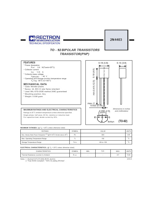
2010-5ELECTRICAL CHARACTERISTICS ( @ T A = 25C unless otherwise noted)MAXIMUM TATINGES ( @ T A = 25C unless otherwise noted)Notes :CHARACTERISTICSSYMBOL UNITS417oC/WThermal Resistance Junction to AmbientRATINGSMax. Steady State Power Dissipation (1) @TA=25oC Derate above 25CMax. Operating Temperature Range Storage Temperature RangeSYMBOL P D T J T STGR q JAVALUE MAX.-TYP.-MIN.UNITS mW6001. Alumina=0.4*0.3*0.024in.99.5% alumina2. "Fully ROHS Compliant", "100% Sn plating (Pb-free)".150-55 to +150o C oCTRANSISTOR(PNP)ELECTRICAL CHARACTERISTICS(@TA=25O C unless otherwise noted)OFF CHARACTERISTICSON CHARACTERISTICS (1)ChatacteristicCollector-Emitter Breakdown Voltage(1) (I C = -1.0 mAdc, I B = 0) Collector-Base Breakdown Voltage (I C = -0.1mAdc, I E = 0)Emitter-Base Breakdown Voltage (I E = -0.1mAdc, I C = 0)Base Cutoff Current (V CE = -35Vdc, V BE(off)= -0.4Vdc)Collector Cutoff Current (V CE = -35Vdc, V EB = -0.4Vdc)DC Current Gain (I C = -0.1mAdc, V CE = -1.0Vdc)(I C = -10mAdc, V CE = -1.0Vdc)(I C = -1.0mAdc, V CE = -1.0Vdc)V (BR)CEO -40-Vdc V (BR)CBO -40-Vdc V (BR)EBO-5.0-Vdc I CEXI BEV --0.1--0.1hFE30--60-100-100300uAdcuAdc Symbol Min Max Unit(I C = -150mAdc, V CE = -2.0Vdc)Collector-Emitter Saturation Voltage (1) (I C = -150mAdc, I B = -15mAdc)(I C = -500mAdc, I B = -50mAdc)(I C = -500mAdc, V CE = -2.0Vdc)Vdc V CE(sat)20---0.4--0.75VdcV BE(sat)-0.75-0.95--1.3Base-Emitter Saturation Voltage (1) (I C = -150mAdc, I B = -15mAdc)(I C = -500mAdc, I B =-50mAdc)SMALL-SIGNAL CHARACTERISTICSSWITCHING CHARACTERISTICSf T 200-MHz Current-Gain-Bandwidth Product (I C = -20mAdc, V CE = -10Vdc, f= 100MHz)C cb C eb -8.5pF pF t d t r t s t f----nsnsh ie -301.515kohms h re 0.18.060500X 10-4h fe 1.0100-h oe225301520umhosOutput Capacitance (V CB = -10Vdc, I E = 0, f= 1.0MHz)Input Capacitance (V EB = -0.5Vdc, I C = 0, f= 1.0MHz)Voltage Feedback Ratio (V CE = -10Vdc, I C = -1.0mAdc, f= 1.0kHz)Output Admittance (V CE = -10Vdc, I C = -1.0mAdc, f= 1.0kHz)(V CC = -30Vdc, V EB = -2.0Vdc, I C = -150mAdc, I B1= -15mAdc)(V CC = -30Vdc, I C = -150mAdc, I B1= I B2= -15mAdc)Input lmpedance (V CE = -10Vdc, I C = -1.0mAdc, f= 1.0kHz)Small-Signal Current Gain (V CE = -10Vdc, I C = -1.0mAdc, f= 1.0kHz)Delay Time Rise Time Storage Time Fall TimeNote :Pulse Test: Pulse Width <300ms,Duty Cycle <2.0%--RATING AND CHARACTERISTICS CURVES ( )Figure 1. CapacitancesFigure 3. Turn-On TimeFigure 5. Storage Time0.1 0.2 0.3 0.5 0.7 1.0 2.0 3.0 5.0 10 20 3010 20 30 50 70 100 200 300 500C A P A C I T A N C E (p F )t s ',S T O R A G E T I M E (n s )t , T I M E (n s )t , T I M E (n s )Q , C H A R G E (n C )REVERSE VOLTAGE (V)I C ,COLLECTOR CURRENT (mA)I C , COLLECTOR CURRENT (mA)I C ,COLLECTOR CURRENT (mA)Figure 4. Rise Times10203050701007.05.010 20 30 50 70 100 200 300 50010 20 30 50 70 100 200 300 500I C ,COLLECTOR CURRENT (mA)10 20 30 50 70 100 200 300 500Figure 2. Charge Data0.20.30.50.71.0100.12.03.05.07.025OC100O C2N4403RATING AND CHARACTERISTICS CURVES ()h o e , O U T P U T A D M I T T A N C E (u m h o s )h r e , V O L T A G E F E E D B A C K R A T I O (X 10-4)0.1 0.2 0.3 0.5 0.7 1.0 2.0 3.0 5.0 7.0 100.1 0.2 0.3 0.5 0.7 1.0 2.0 3.0 5.0 7.0 1050 100 200 500 1.0k 2.0k 5.0k 10k 20k 50kN F , N O I S E F I G U R E (d B )N F ,N O I S E F I G U R E (d B )Figure 6.Frequency EffectsI C , COLLECTOR CURRENT (mAdc)I C , COLLECTOR CURRENT (mAdc)Figure 8.Cuttent GainFigure 9.Input ImpedanceR S , SOURCE RESISTANCE (OHMS)Figure 7.Source Resistance EffectsI C , COLLECTOR CURRENT (mAdc)I C , COLLECTOR CURRENT (mAdc)Figure 11.Temperature CoefficientsFigure 10.Voltage Feedback Ratio 0.1 0.2 0.3 0.5 0.7 1.0 2.0 3.0 5.0 7.0 100.1 0.2 0.3 0.5 0.7 1.0 2.0 3.0 5.0 7.0 10f, FREQUENCY (KHz)46810200.01 0.02 0.05 0.1 0.2 0.5 1.0 2.0 5.0 10 20 50 100V CE = -10Vdc, T A = 25CBandwidth = 1.0Hz2N4403RATING AND CHARACTERISTICS CURVES ()Figure 12. DC Current GainFigure 13. Collector Saturation RegionFigure 14. "ON" Voltages Figure 15. Temperature Coefficients0.1 0.2 0.3 0.5 0.7 1.0 2.0 3.0 5.0 7.0 10 20 30 50 70 100 200 300 5000.005 0.01 0.02 0.03 0.05 0.07 0.1 0.2 0.3 0.5 0.7 1.0 2.0 3.0 5.0 7.0 10 20 30 500.1 0..2 0.5 1.0 2.0 5.0 10 20 50 100 200 5000.1 0..2 0.5 1.0 2.0 5.0 10 20 50 100 200 500h F E , N O R M A L I Z E D C U R R E N T G A I NV C E , C O L L E C T O R - E M I T T E R V O L T A G E (V )V O L T A G E (V )C O E F F I C I E N T (m V /OC )I C , COLLECTOR CURRENT (mA)I B , BASE CURRENT (mA)I C , COLLECTOR CURRENT (mA)I C , COLLECTOR CURRENT (mA)0.40.60.81.00.20.30.50.71.03.00.22.030442NRectron Inc reserves the right to make changes without notice to any productspecification herein, to make corrections, modifications, enhancements or other changes. Rectron Inc or anyone on its behalf assumes no responsibility or liabi- lity for any errors or inaccuracies. Data sheet specifications and its information contained are intended to provide a product description only. "Typical" paramet- ers which may be included on RECTRON data sheets and/ or specifications ca- n and do vary in different applications and actual performance may vary over ti- me. Rectron Inc does not assume any liability arising out of the application or use of any product or circuit.Rectron products are not designed, intended or authorized for use in medical, life-saving implant or other applications intended for life-sustaining or other rela- ted applications where a failure or malfunction of component or circuitry may di- rectly or indirectly cause injury or threaten a life without expressed written appr- oval of Rectron Inc. Customers using or selling Rectron components for use in such applications do so at their own risk and shall agree to fully indemnify Rect- ron Inc and its subsidiaries harmless against all claims, damages and expendit- ures.DISCLAIMER NOTICE。