MTJ-665X1中文资料
- 格式:pdf
- 大小:156.54 KB
- 文档页数:1

Atmel芯片新命名型号对照表ATTINY28L ATMEL ATMLU701 DIP ATTINY26L ATMEL ATMLU702 DIP ATTINY26 ATMEL ATMLU703 DIP ATTINY24 ATMEL ATMLU704 DIP ATTINY2313V ATMEL ATMLU705 DIP ATTINY2313 ATMEL ATMLU706 DIP ATTINY15L ATMEL ATMLU707 DIP ATTINY13V ATMEL ATMLU708 DIP ATTINY13 ATMEL ATMLU709 DIP ATTINY11L ATMEL ATMLU710 DIP ATMEGA8L ATMEL ATMLU711 DIP ATMEGA88V ATMEL ATMLU712 DIP ATMEGA88 ATMEL ATMLU713 DIP ATMEGA8535L ATMEL ATMLU714 DIP ATMEGA8535 ATMEL ATMLU715 DIP ATMEGA8515L ATMEL ATMLU716 DIP ATMEGA8515 ATMEL ATMLU717 DIP ATMEGA8 ATMEL ATMLU718 DIP ATMEGA64L ATMEL ATMLU719 DIP ATMEGA64 ATMEL ATMLU720 DIP ATMEGA640V ATMEL ATMLU721 DIP ATMEGA48V ATMEL ATMLU722 DIP ATMEGA48 ATMEL ATMLU723 DIP ATMEGA32L ATMEL ATMLU724 DIP ATMEGA325V ATMEL ATMLU725 DIP ATMEGA32 ATMEL ATMLU726 DIP ATMEGA16L ATMEL ATMLU727 DIP ATMEGA169V ATMEL ATMLU728 DIP ATMEGA169PV ATMEL ATMLU729 DIP ATMEGA169P ATMEL ATMLU730 DIP ATMEGA168V ATMEL ATMLU731 DIP ATMEGA168 ATMEL ATMLU732 DIP ATMEGA162V ATMEL ATMLU733 DIP ATMEGA162 ATMEL ATMLU734 DIP ATMEGA16 ATMEL ATMLU735 DIP ATMEGA128L ATMEL ATMLU736 DIP ATMEGA128 ATMEL ATMLU737 DIP ATMEGA1280V ATMEL ATMLU738 DIP ATJTAGICE2 ATMEL ATMLU739 DIPATF20V8B ATMEL ATMLU740 DIPATF16V8BQL ATMEL ATMLU741 DIP ATF16V8B ATMEL ATMLU742 DIPATF1508AS ATMEL ATMLU743 DIP ATF1502AS ATMEL ATMLU744 DIP ATAVRISP2 ATMEL ATMLU745 DIP ATAVRDRAGON ATMEL ATMLU746 DIP AT93C66A ATMEL ATMLU747 DIPAT93C56A ATMEL ATMLU748 DIPAT93C46DN ATMEL ATMLU749 DIPAT93C46DH ATMEL ATMLU750 DIPAT93C46 ATMEL ATMLU751 DIPAT91SAM ATMEL ATMLU752 DIPAT91SAM9263 ATMEL ATMLU801 DIP AT91SAM9261S ATMEL ATMLU802 DIP AT91SAM9261 ATMEL ATMLU803 DIP AT91SAM9260 ATMEL ATMLU804 DIP AT91SAM7X ATMEL ATMLU805 DIPAT91SAM7X256 ATMEL ATMLU806 DIP AT91SAM7SE32 ATMEL ATMLU807 DIP AT91SAM7S64 ATMEL ATMLU808 DIP AT91SAM7S32 ATMEL ATMLU809 DIP AT91SAM7S321 ATMEL ATMLU810 DIP AT91SAM7S256 ATMEL ATMLU811 DIP AT91RM9200 ATMEL ATMLU812 DIP AT91M55800A ATMEL ATMLU813 DIP AT91M40800 ATMEL ATMLU814 DIPAT90CAN32 ATMEL ATMLU815 DIPAT90CAN128 ATMEL ATMLU816 DIP AT89S8253 ATMEL ATMLU817 DIPAT89S58 ATMEL ATMLU818 DIPAT89S54 ATMEL ATMLU819 DIPAT89S52 ATMEL ATMLU820 DIPAT89S51 ATMEL ATMLU821 DIPAT89LV51 ATMEL ATMLU822 DIPAT89LS52 ATMEL ATMLU823 DIPAT89C55WD ATMEL ATMLU824 DIPAT89C52 ATMEL ATMLU825 DIPAT89C51RD2 ATMEL ATMLU826 DIP AT89C51RC2 ATMEL ATMLU827 DIP AT89C51RC ATMEL ATMLU828 DIPAT89C51RC2 ATMEL ATMLU829 DIPAT89C51ED2 ATMEL ATMLU831 DIPAT89C51CC01UA ATMEL ATMLU832 DIP AT89C51CC01CA ATMEL ATMLU833 DIP AT89C51AU2 ATMEL ATMLU834 DIPAT89C5131A ATMEL ATMLU835 DIPAT89C51 ATMEL ATMLU836 DIPAT89C4051 ATMEL ATMLU837 DIPAT89C2051 ATMEL ATMLU838 DIPAT88SC153 ATMEL ATMLU839 DIPAT88SC0104C ATMEL ATMLU840 DIP AT49BV512 ATMEL ATMLU841 DIPAT49BV322DT ATMEL ATMLU842 DIP AT49BV040B ATMEL ATMLU843 DIPAT47BV163A ATMEL ATMLU844 DIPAT45DB642DU ATMEL ATMLU845 DIP AT45DB321DU ATMEL ATMLU846 DIP AT45DB321D ATMEL ATMLU847 DIPAT45DB161DU ATMEL ATMLU848 DIP AT45DB161D ATMEL ATMLU849 DIPAT45DB081D ATMEL ATMLU850 DIPAT45DB041D ATMEL ATMLU851 DIPAT45DB021B ATMEL ATMLU852 DIPAT29LV512 ATMEL ATMLU901 DIPAT29LV040A ATMEL ATMLU902 DIPAT29LV020 ATMEL ATMLU903 DIPAT29C040A ATMEL ATMLU904 DIPAT29C020 ATMEL ATMLU905 DIPAT29C010A ATMEL ATMLU906 DIPAT28C64B ATMEL ATMLU907 DIPAT28C256 ATMEL ATMLU908 DIPAT28BV256 ATMEL ATMLU909 DIPAT27C512R ATMEL ATMLU910 DIPAT27C256R ATMEL ATMLH701 SOPAT27C040 ATMEL ATMLH702 SOPAT27C010 ATMEL ATMLH703 SOPAT27BV256 ATMEL ATMLH704 SOPAT26DF321 ATMEL ATMLH705 SOPAT26DF161 ATMEL ATMLH706 SOPAT26DF081A ATMEL ATMLH707 SOPAT25F512AN ATMEL ATMLH708 SOPAT25F1024AN ATMEL ATMLH709 SOPAT25256AN ATMEL ATMLH711 SOP AT25128A ATMEL ATMLH712 SOPAT24C64CN ATMEL ATMLH713 SOP AT24C64AN ATMEL ATMLH714 SOP AT24C64A ATMEL ATMLH715 SOP AT24C512N ATMEL ATMLH716 SOP AT24C512B ATMEL ATMLH717 SOP AT24C512BN ATMEL ATMLH718 SOP AT24C512 ATMEL ATMLH719 SOPAT24C32CN ATMEL ATMLH720 SOP AT24C32AN ATMEL ATMLH721 SOP AT24C32A ATMEL ATMLH722 SOP AT24C256N ATMEL ATMLH723 SOP AT24C256B ATMEL ATMLH724 SOP AT24C256BN ATMEL ATMLH725 SOP AT24C256B ATMEL ATMLH726 SOP AT24C16BN ATMEL ATMLH727 SOP AT24C16AN ATMEL ATMLH728 SOP AT24C16A ATMEL ATMLH729 SOP AT24C128N ATMEL ATMLH730 SOP AT24C128 ATMEL ATMLH731 SOPAT24C08AN ATMEL ATMLH732 SOP AT24C08A ATMEL ATMLH733 SOP AT24C04N ATMEL ATMLH734 SOP AT24C04BN ATMEL ATMLH735 SOP AT24C04 ATMEL ATMLH736 SOPAT24C02B ATMEL ATMLH737 SOP AT24C02BN ATMEL ATMLH738 SOP AT24C02B ATMEL ATMLH739 SOP AT24C01B ATMEL ATMLH740 SOP AT24C01BN ATMEL ATMLH741 SOP ATTINY28L ATMEL ATMLU701 SOP ATTINY26L ATMEL ATMLU702 SOP ATTINY26 ATMEL ATMLU703 SOP ATTINY24 ATMEL ATMLU704 SOP ATTINY2313V ATMEL ATMLU705 SOP ATTINY2313 ATMEL ATMLU706 SOP ATTINY15L ATMEL ATMLU707 SOP ATTINY13V ATMEL ATMLU708 SOP ATTINY13 ATMEL ATMLU709 SOP ATTINY11L ATMEL ATMLU710 SOPATMEGA88V ATMEL ATMLU712 SOP ATMEGA88 ATMEL ATMLU713 SOP ATMEGA8535L ATMEL ATMLU714 SOP ATMEGA8535 ATMEL ATMLU715 SOP ATMEGA8515L ATMEL ATMLU716 SOP ATMEGA8515 ATMEL ATMLU717 SOP ATMEGA8 ATMEL ATMLU718 SOP ATMEGA64L ATMEL ATMLU719 SOP ATMEGA64 ATMEL ATMLU720 SOP ATMEGA640V ATMEL ATMLU721 SOP ATMEGA48V ATMEL ATMLU722 SOP ATMEGA48 ATMEL ATMLU723 SOP ATMEGA32L ATMEL ATMLU724 SOP ATMEGA325V ATMEL ATMLU725 SOP ATMEGA32 ATMEL ATMLU726 SOP ATMEGA16L ATMEL ATMLU727 SOP ATMEGA169V ATMEL ATMLU728 SOP ATMEGA169PV ATMEL ATMLU729 SOP ATMEGA169P ATMEL ATMLU730 SOP ATMEGA168V ATMEL ATMLU731 SOP ATMEGA168 ATMEL ATMLU732 SOP ATMEGA162V ATMEL ATMLU733 SOP ATMEGA162 ATMEL ATMLU734 SOP ATMEGA16 ATMEL ATMLU735 SOP ATMEGA128L ATMEL ATMLU736 SOP ATMEGA128 ATMEL ATMLU737 SOP ATMEGA1280V ATMEL ATMLU738 SOP ATJTAGICE2 ATMEL ATMLU739 SOP ATF20V8B ATMEL ATMLU740 SOPATF16V8BQL ATMEL ATMLU741 SOP ATF16V8B ATMEL ATMLU742 SOPATF1508AS ATMEL ATMLU743 SOP ATF1502AS ATMEL ATMLU744 SOP ATAVRISP2 ATMEL ATMLU745 SOP ATAVRDRAGON ATMEL ATMLU746 SOP AT93C66A ATMEL ATMLU747 SOPAT93C56A ATMEL ATMLU748 SOPAT93C46DN ATMEL ATMLU749 SOPAT93C46DH ATMEL ATMLU750 SOPAT93C46 ATMEL ATMLU751 SOPAT91SAM ATMEL ATMLU752 SOPAT91SAM9261S ATMEL ATMLU802 SOP AT91SAM9261 ATMEL ATMLU803 SOP AT91SAM9260 ATMEL ATMLU804 SOP AT91SAM7X ATMEL ATMLU805 SOPAT91SAM7X256 ATMEL ATMLU806 SOP AT91SAM7SE32 ATMEL ATMLU807 SOP AT91SAM7S64 ATMEL ATMLU808 SOP AT91SAM7S32 ATMEL ATMLU809 SOP AT91SAM7S321 ATMEL ATMLU810 SOP AT91SAM7S256 ATMEL ATMLU811 SOP AT91RM9200 ATMEL ATMLU812 SOPAT91M55800A ATMEL ATMLU813 SOP AT91M40800 ATMEL ATMLU814 SOPAT90CAN32 ATMEL ATMLU815 SOPAT90CAN128 ATMEL ATMLU816 SOPAT89S8253 ATMEL ATMLU817 SOPAT89S58 ATMEL ATMLU818 SOPAT89S54 ATMEL ATMLU819 SOPAT89S52 ATMEL ATMLU820 SOPAT89S51 ATMEL ATMLU821 SOPAT89LV51 ATMEL ATMLU822 SOPAT89LS52 ATMEL ATMLU823 SOPAT89C55WD ATMEL ATMLU824 SOPAT89C52 ATMEL ATMLU825 SOPAT89C51RD2 ATMEL ATMLU826 SOPAT89C51RC2 ATMEL ATMLU827 SOPAT89C51RC ATMEL ATMLU828 SOPAT89C51RC2 ATMEL ATMLU829 SOPAT89C51RB2 ATMEL ATMLU830 SOPAT89C51ED2 ATMEL ATMLU831 SOPAT89C51CC01UA ATMEL ATMLU832 SOP AT89C51CC01CA ATMEL ATMLU833 SOP AT89C51AU2 ATMEL ATMLU834 SOPAT89C5131A ATMEL ATMLU835 SOPAT89C51 ATMEL ATMLU836 SOPAT89C4051 ATMEL ATMLU837 SOPAT89C2051 ATMEL ATMLU838 SOPAT88SC153 ATMEL ATMLU839 SOPAT88SC0104C ATMEL ATMLU840 SOP AT49BV512 ATMEL ATMLU841 SOPAT49BV322DT ATMEL ATMLU842 SOPAT47BV163A ATMEL ATMLU844 SOP AT45DB642DU ATMEL ATMLU845 SOP AT45DB321DU ATMEL ATMLU846 SOP AT45DB321D ATMEL ATMLU847 SOP AT45DB161DU ATMEL ATMLU848 SOP AT45DB161D ATMEL ATMLU849 SOP AT45DB081D ATMEL ATMLU850 SOP AT45DB041D ATMEL ATMLU851 SOP AT45DB021B ATMEL ATMLU852 SOP AT29LV512 ATMEL ATMLU901 SOP AT29LV040A ATMEL ATMLU902 SOP AT29LV020 ATMEL ATMLU903 SOP AT29C040A ATMEL ATMLU904 SOP AT29C020 ATMEL ATMLU905 SOPAT29C010A ATMEL ATMLU906 SOP AT28C64B ATMEL ATMLU907 SOPAT28C256 ATMEL ATMLU908 SOPAT28BV256 ATMEL ATMLU909 SOP AT27C512R ATMEL ATMLU910 SOP AT27C256R ATMEL ATMLH701 DIPAT27C040 ATMEL ATMLH702 DIPAT27C010 ATMEL ATMLH703 DIPAT27BV256 ATMEL ATMLH704 DIPAT26DF321 ATMEL ATMLH705 DIPAT26DF161 ATMEL ATMLH706 DIPAT26DF081A ATMEL ATMLH707 DIP AT25F512AN ATMEL ATMLH708 DIP AT25F1024AN ATMEL ATMLH709 DIP AT25DF041A ATMEL ATMLH710 DIP AT25256AN ATMEL ATMLH711 DIPAT25128A ATMEL ATMLH712 DIPAT24C64CN ATMEL ATMLH713 DIPAT24C64AN ATMEL ATMLH714 DIPAT24C64A ATMEL ATMLH715 DIPAT24C512N ATMEL ATMLH716 DIPAT24C512B ATMEL ATMLH717 DIPAT24C512BN ATMEL ATMLH718 DIP AT24C512 ATMEL ATMLH719 DIPAT24C32CN ATMEL ATMLH720 DIPAT24C32AN ATMEL ATMLH721 DIPAT24C32A ATMEL ATMLH722 DIPAT24C256B ATMEL ATMLH724 DIP AT24C256BN ATMEL ATMLH725 DIP AT24C256B ATMEL ATMLH726 DIP AT24C16BN ATMEL ATMLH727 DIP AT24C16AN ATMEL ATMLH728 DIP AT24C16A ATMEL ATMLH729 DIP AT24C128N ATMEL ATMLH730 DIP AT24C128 ATMEL ATMLH731 DIP AT24C08AN ATMEL ATMLH732 DIP AT24C08A ATMEL ATMLH733 DIP AT24C04N ATMEL ATMLH734 DIP AT24C04BN ATMEL ATMLH735 DIP AT24C04 ATMEL ATMLH736 DIPAT24C02B ATMEL ATMLH737 DIP AT24C02BN ATMEL ATMLH738 DIP AT24C02B ATMEL ATMLH739 DIP AT24C01B ATMEL ATMLH740 DIP AT24C01BN ATMEL ATMLH741 DIP 不全,不过我可是第一个回答的啊。


MPS6601, MPS6602 (NPN)MPS6651, MPS6652 (PNP)MPS6602 and MPS6652 are Preferred DevicesAmplifier TransistorsFeatures•V oltage and Current are Negative for PNP Transistors •Pb−Free Packages are Available*MAXIMUM RATINGSRatingSymbol Value Unit Collector −Emitter VoltageMPS6601/6651MPS6602/6652V CEO2540VdcCollector −Base VoltageMPS6601/6651MPS6602/6652V CBO2530VdcEmitter −Base Voltage V EBO 4.0Vdc Collector Current − ContinuousI C 1000mAdc Total Device Dissipation @ T A = 25°C Derate above 25°CP D 6255.0W mW/°C Total Device Dissipation @ T C = 25°C Derate above 25°CP D 1.512W mW/°C Operating and Storage Junction Temperature RangeT J , T stg−55 to +150°C THERMAL CHARACTERISTICSCharacteristicSymbol Max UnitThermal Resistance, Junction−to−Ambient (Note 1)R q JA 200°C/W Thermal Resistance, Junction−to−CaseR q JC83.3°C/WStresses exceeding Maximum Ratings may damage the device. Maximum Ratings are stress ratings only. Functional operation above the Recommended Operating Conditions is not implied. Extended exposure to stresses above the Recommended Operating Conditions may affect device reliability.1.R q JA is measured with the device soldered into a typical printed circuit board.*For additional information on our Pb−Free strategy and soldering details, please download the ON Semiconductor Soldering and Mounting Techniques Reference Manual, SOLDERRM/D.Preferred devices are recommended choices for future use and best overall value.See detailed ordering and shipping information in the package dimensions section on page 7 of this data sheet.ORDERING INFORMATIONELECTRICAL CHARACTERISTICS (T A = 25°C unless otherwise noted)Characteristic Symbol Min Max Unit OFF CHARACTERISTICSCollector−Emitter Breakdown Voltage(I C = 1.0 mAdc, I B = 0)MPS6601/6651MPS6602/6652V(BR)CEO2540−−VdcCollector−Base Breakdown Voltage(I C = 100 m Adc, I E = 0)MPS6601/6651MPS6602/6652V(BR)CBO2540−−VdcEmitter−Base Breakdown Voltage(I E = 10 m Adc, I C = 0)V(BR)EBO 4.0−VdcCollector Cutoff Current(V CE = 25 Vdc, I B = 0)MPS6601/6651 (V CE = 30 Vdc, I B = 0)MPS6602/6652I CES−−0.10.1m AdcCollector Cutoff Current(V CB = 25 Vdc, I E = 0)MPS6601/6651 (V CB = 30 Vdc, I E = 0)MPS6602/6652I CBO−−0.10.1m AdcON CHARACTERISTICSDC Current Gain(I C = 100 mAdc, V CE = 1.0 Vdc) (I C = 500 mAdc, V CE = 1.0 Vdc) (I C = 1000 mAdc, V CE = 1.0 Vdc)h FE505030−−−−Collector−Emitter Saturation Voltage(I C = 1000 mAdc, I B = 100 mAdc)V CE(sat)−0.6VdcBase−Emitter On Voltage(I C = 500 mAdc, V CE = 1.0 Vdc)V BE(on)− 1.2Vdc SMALL−SIGNAL CHARACTERISTICSCurrent−Gain — Bandwidth Product(I C = 50 mAdc, V CE = 10 Vdc, f = 100 MHz)f T100−MHzOutput Capacitance(V CB = 10 Vdc, I E = 0, f = 1.0 MHz)C obo−30pF SWITCHING CHARACTERISTICSDelay Time(V CC = 40 Vdc, I C = 500 mAdc,I B1 = 50 mAdc,t p w 300 ns Duty Cycle)t d−25nsRise Time t r−30ns Storage Time t s−250ns Fall Time t f−50nsFigure 1. Thermal Responset, TIME (SECONDS)0.0010.0020.0050.010.020.050.10.20.51.02.05.01020501000.030.020.10.070.050.010.30.21.00.70.5r (t ), N O R M A L I Z E D E F F E C T I V E T R A N S I E N T T H E R M A L R E S I S T A N C EFigure 2. Switching Time Test CircuitsOUTPUTTURN−ON TIME S t 6.0 pFt r = 3.0 ns+10VOUTPUTTURN−OFF TIME S t 6.0 pFt r = 3.0 ns*Total Shunt Capacitance of Test Jig and Connectors For PNP Test Circuits, Reverse All Voltage PolaritiesFigure 7. On Voltages Figure 8. On Voltages3002001007050303002001007050301010001.0I C , COLLECTOR CURRENT (mA)1.00.80.60.40.20I C , COLLECTOR CURRENT (mA)−10−1000−1.0−100100f T , C U R R E N T G A I N B A N D W I D T H P R O D U C T (M H z )V , V O L T A G E (V O L T S )NPNPNPF E h , C U R R E N TG A I NFigure 13. MPS6601/6602 Switching TimesFigure 14. MPS6651/6652 Switching Times806040200108.06.04.02.0020100010I C , COLLECTOR CURRENT (mA)200100502010I C , COLLECTOR CURRENT (mA)−20−1000−10−100100C , C A P A C I T A N C E (p F )N F , N O I S E F I G U R E (d B )t , T I M E (N S )NPNPNP502005001 k 5003 k 10 k 5 k −50−200−500Figure 15. Base−Emitter TemperatureCoefficientFigure 16. Base−Emitter TemperatureCoefficientFigure 17. Safe Operating Area Figure 18. Safe Operating AreaFigure 19. MPS6601/6602 Saturation Region Figure 20. MPS6651/6652 Saturation Region10010001.0I C , COLLECTOR CURRENT (mA)−0.8−1.2−1.6−2.0−2.4−2.8I C , COLLECTOR CURRENT (mA)−100−1000−1.0101.0V CE , COLLECTOR−EMITTER VOLTAGE 500200*********V CE , COLLECTOR−EMITTER VOLTAGE−10−40−1.0−500−200−100−50−20−10−20200.1100.01I B , BASE CURRENT (mA)1.00.80.60.40.20I B , BASE CURRENT (mA)−0.1−100−0.01−1.0−0.8−0.6−0.4−0.20−1.01.0R V B , T E M P ER A T U R E C O E F F I C I E N T (m V / C )I C ,C O L L E C T O R C U R R E N T (m A )NPNPNP10q °−10−2.0−5.0−1 k 2.05.0401 k I C , C O L L E C T O R C U R R E N T (m A )−10100, C O L L E C T O R V O L T A G E (V O L T S )V C E , C O L L E C T O R V O L T A G E (V O L T S )V C EORDERING INFORMATIONDevice Package Shipping†MPS6601TO−92 (TO−226)5000 Units / BoxMPS6601G TO−92 (TO−226)(Pb−Free)MPS6601RLRA TO−92 (TO−226)2000 Units / Tape & ReelMPS6601RLRAG TO−92 (TO−226)(Pb−Free)MPS6602TO−92 (TO−226)5000 Units / BoxMPS6602G TO−92 (TO−226)(Pb−Free)MPS6602RLRA TO−92 (TO−226)2000 Units / Tape & ReelMPS6602RLRAG TO−92 (TO−226)(Pb−Free)MPS6651TO−92 (TO−226)5000 Units / BoxMPS6651G TO−92 (TO−226)(Pb−Free)MPS6652TO−92 (TO−226)5000 Units / BoxMPS6652G TO−92 (TO−226)(Pb−Free)MPS6652RLRA TO−92 (TO−226)2000 Units / Tape & ReelMPS6652RLRAG TO−92 (TO−226)(Pb−Free)MPS6652RLRP TO−92 (TO−226)2000 Units / Tape & Ammo BoxMPS6652RLRPG TO−92 (TO−226)(Pb−Free)†For information on tape and reel specifications, including part orientation and tape sizes, please refer to our Tape and Reel Packaging Specifications Brochure, BRD8011/D.PACKAGE DIMENSIONSNOTES:1.DIMENSIONING AND TOLERANCING PER ANSI Y14.5M, 1982.2.CONTROLLING DIMENSION: INCH.3.CONTOUR OF PACKAGE BEYOND DIMENSION R IS UNCONTROLLED.4.LEAD DIMENSION IS UNCONTROLLED IN P AND BEYOND DIMENSION K MINIMUM.PLANEDIM MIN MAX MIN MAX MILLIMETERSINCHES A 0.1750.205 4.45 5.20B 0.1700.210 4.32 5.33C 0.1250.165 3.18 4.19D 0.0160.0210.4070.533G 0.0450.055 1.15 1.39H 0.0950.105 2.42 2.66J 0.0150.0200.390.50K 0.500−−−12.70−−−L 0.250−−− 6.35−−−N 0.0800.105 2.04 2.66P −−−0.100−−− 2.54R 0.115−−− 2.93−−−V0.135−−−3.43−−−TO−92 (TO−226)CASE 29−11ISSUE ALSTYLE 1:PIN 1.EMITTER2.BASE3.COLLECTORON Semiconductor and are registered trademarks of Semiconductor Components Industries, LLC (SCILLC). SCILLC reserves the right to make changes without further notice to any products herein. SCILLC makes no warranty, representation or guarantee regarding the suitability of its products for any particular purpose, nor does SCILLC assume any liability arising out of the application or use of any product or circuit, and specifically disclaims any and all liability, including without limitation special, consequential or incidental damages.“Typical” parameters which may be provided in SCILLC data sheets and/or specifications can and do vary in different applications and actual performance may vary over time. All operating parameters, including “Typicals” must be validated for each customer application by customer’s technical experts. SCILLC does not convey any license under its patent rights nor the rights of others. SCILLC products are not designed, intended, or authorized for use as components in systems intended for surgical implant into the body, or other applications intended to support or sustain life, or for any other application in which the failure of the SCILLC product could create a situation where personal injury or death may occur. Should Buyer purchase or use SCILLC products for any such unintended or unauthorized application, Buyer shall indemnify and hold SCILLC and its officers, employees, subsidiaries, affiliates,and distributors harmless against all claims, costs, damages, and expenses, and reasonable attorney fees arising out of, directly or indirectly, any claim of personal injury or death associated with such unintended or unauthorized use, even if such claim alleges that SCILLC was negligent regarding the design or manufacture of the part. SCILLC is an Equal Opportunity/Affirmative Action Employer. This literature is subject to all applicable copyright laws and is not for resale in any manner.PUBLICATION ORDERING INFORMATION。
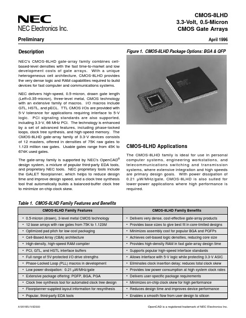
April 1996NEC Electronics Inc.A10616EU1V0DS00CMOS-8LHD3.3-Volt, 0.5-Micron CMOS Gate ArraysPreliminary DescriptionNEC's CMOS-8LHD gate-array family combines cell-based-level densities with the fast time-to-market and low development costs of gate arrays. With a unique heterogeneous cell architecture, CMOS-8LHD provides the very dense logic and RAM capabilities required to build devices for fast computer and communications systems.NEC delivers high-speed, 0.5-micron, drawn gate length (Leff=0.35-micron), three-level metal, CMOS technology with an extensive family of macros. I/O macros include GTL, HSTL, and pECL. TTL CMOS I/Os are provided with 5-V tolerance for applications requiring interface to 5-V logic. PCI signaling standards are also supported,including 3.3-V, 66 MHz PCI. The technology is enhanced by a set of advanced features, including phase-locked loops, clock tree synthesis, and high-speed memory. The CMOS-8LHD gate-array family of 3.3-V devices consists of 12 masters, offered in densities of 75K raw gates to 1.123 million raw gates. Usable gates range from 45K to 674K used gates.The gate-array family is supported by NEC's OpenCAD ®design system, a mixture of popular third-party EDA tools,and proprietary NEC tools. NEC proprietary tools include the GALET floorplanner, which helps to reduce design time and improve design speed, and a clock tree synthesis tool that automatically builds a balanced-buffer clock tree to minimize on-chip clock skew.Figure 1. CMOS-8LHD Package Options: BGA & QFPTable 1. CMOS-8LHD Family Features and BenefitsCMOS-8LHD ApplicationsThe CMOS-8LHD family is ideal for use in personal computer systems, engineering workstations, and telecommunications switching and transmission systems, where extensive integration and high speeds are primary design goals. With power dissipation of 0.21 µW/MHz/gate, CMOS-8LHD is also suited for lower-power applications where high performance is required.OpenCAD is a registered trademark of NEC Electronics Inc.CMOS-8LHD2Cell-Based Array ArchitectureThe CMOS-8LHD gate-array family is built with the Cell-Based Array (CBA) architecture licensed from the Silicon Architects Group of Synopsys. CBA architecture uses two types of cells: compute cells and drive cells.This heterogeneous cell architecture enables very high-density design. Compute cells are used to optimize intramacro logic. Drive cells are optimized for intermacro interconnect. The two cell types are also used to build macros with up to three different power/performance/area points.CBA has a rich macrocell library that is optimized for synthesis. RAM blocks are efficiently created from the CBA architecture, using compute cells as memory cores, and sense amplifiers and drive cells as word and address predecoder drivers.As shown in Figure 2, CBA is divided into I/O and array regions. The I/O region contains input and output buffers. The array region contains the gates used to build logic, RAM blocks, and other design features.Power Rail ArchitectureCMOS-8LHD provides additional flexibility for mixedvoltage system designs. As shown in Figure 2, the arrays contain two power rails: a 3.3-V rail, and V DD2.The V DD2 rail is used for interfaces such as 5-V PCI buffers where a clamping diode allows protection for up to an 11-V voltage spike, per the PCI revision 2.1specification.Figure 2. CBA Layout and Cell ConfigurationThe V DD2 rail is separated into sections to give flexibility for including two or more buses requiring special I/O voltage on one device. Each section can operate as an independent voltage zone, and sections can be linked together to form common voltage zones.Packaging and TestNEC utilizes BIST test structures for RAM testing. NEC also offers advanced packaging solutions including Plastic Ball Grid Arrays (PBGA), Plastic Quad Flat Packs (PQFP), and Pin Grid Arrays (PGA). Please call your local NEC ASIC design center representative for a listing of available master/package combinations.PublicationsThis data sheet contains preliminary specifications for the CMOS-8LHD gate-array family. Additional infor-mation will be available in NEC's CMOS-8LHD Block Library and CMOS-8LHD Design Manual . Call your local NEC ASIC design center representative or the NEC literature line for additional ASIC design information; see the back of this data sheet for locations and phone numbers.Table 2. CMOS-8LHD Base Array Line-upDevice Raw Gates Used Gates (1)Total Pads66562750404502416466563997925987518866565125216751292126656617963210777925266568202400121440268665692681281608763086657029792017875232466571359744215845356665725008643005184206657362054437232646866575802240481344532(1) Actual gate utilization varies depending on circuit implementation.Utilization is 60% for 3LM.3CMOS-8LHDInput/Output CapacitanceV DD =V I =0-V; f =1 MHzTerminal Symbol Typ Max Unit Input C IN 1020pF Output C OUT 1020pF I/OC I/O1020pF(1)Values include package pin capacitancePower ConsumptionDescription Limits Unit Internal gate (1)0.21µW/MHz Input buffer 2.546µW/MHz Output buffer10.60µW/MHzAbsolute Maximum RatingsPower supply voltage, V DD –0.5 to +4.6-VInput voltage, V I3.3-V input buffer (at V I < V DD + 0.5-V)–0.5 to +4.6-V 3.3-V fail-safe input buffer (at V I < V DD + 0.5-V)–0.5 to +4.6-V 5 V-tolerant (at V I < V DD + 3.0-V)–0.5 to +4.6-V Output Voltage, V O3.3-V output buffer (at V O < V DD + 0.5-V)–0.5 to +4.6-V 5-V-tolerant output buffer (at V O < V DD + 3.0-V)–0.5 to +4.6-V 5-V open-drain output buffer (at V O < V DD + 3.0-V)–0.5 to +4.6-VLatch-up current, I LATCH >1 A (typ)Operating temperature, T OPT –40 to +85°C Storage temperature, T STG–65 to +150°C (1) Assumes 30% internal gate switching at one timeCaution: Exposure to absolute maximum ratings for extended periods may affect device reliability; exceeding the ratings could cause permanent damage. The device should not be operated outside the recommended operating conditions.Recommended Operating ConditionsV DD = 3.3-V ±0.165-V; T j = 0 to +100°C3.3-V Interface 5-V Interface5-V PCI 3.3-V PCIBlock BlockLevel LevelParameterSymbol Min Max Min Max Min Max Min Max Unit I/O power supply voltage V DD 3.0 3.6 3.0 3.6 3.0 5.5 3.0 3.6V Junction temperature T J 0+1000+1000+1000+100°C High-level input voltage V IH 2.0V DD 2.0 5.5 2.0V CC 0.5 V CCV CC V Low-level input voltage V IL 00.800.800.800.3 V CCV Positive trigger voltage V P 1.50 2.70 1.50 2.70————V Negative trigger voltage V N 0.60 1.60.60 1.6————V Hysteresis voltage V H 1.10 1.3 1.10 1.3————V Input rise/fall time t R , t F 0200020002000200ns Input rise/fall time, Schmittt R , t F1010————nsAC CharacteristicsV DD = 3.3-V ±0.3-V; T j = –40 to +125°C ParameterSymbol MinTypMax Unit Conditions Toggle frequency (F611)f TOG356MHzD-F/F; F/O = 2 mmDelay time2-input NAND (F322)t PD181ps F/O = 1; L = 0 mmt PD 186ps F/O = 2; L = typ (0.42 mm)Flip-flop (F611)t PD 573ps F/O = 1; L = 0 mm t PD 688ps F/O = 2; L = typ t SETUP 410ps —t HOLD 540ps —Input buffer (FI01)t PD 268ps F/O = 1; L = 0 mm t PD 312ps F/O = 2; L = typ Output buffer (9 mA) 3.3-V (FO01)t PD 1.316ns C L = 15 pF Output buffer (9 mA) 5-V-tolerant (FV01)t PD 1.228ns C L = 15 pF Output buffer (9 mA) 5-V-swing (FY01)t PD 1.517ns C L = 15 pF Output rise time (9 mA) (FO01)t R 1.347ns C L = 15 pF Output fall time (9 mA) (FO01)t F1.284nsC L = 15 pFCMOS-8LHD4(3)Rating is for only one output operating in this mode for less than 1 second.(4)Normal type buffer: I OH < I OL .(5)Balanced buffer: I OH = I OL .(6)Resistor is called 50ký to maintain consistency with previous families.Notes:(1)Static current consumption increases if an I/O block with on-chip pull-up/pull-down resistor or an oscillator is used. Call an NEC ASIC design center repre-sentative for assistance in calculation.(2)Leakage current is limited by tester capabilities. Specification listed representsthis measurement limitation. Actual values will be significantly lower.DC CharacteristicsV DD = 3.3-V ±0.165-V; T j = 0 to +100°C ParameterSymbol Min Typ Max Unit Conditions Quiescent current (1)µPD66578I DDS 2.0300µA V I = V DD or GND µPD66575, 66573, 66572I DDS 1.0300µA V I = V DD or GND Remaining mastersI DDS 0.5200µA V I = V DD or GND Off-state output leakage current3.3-V buffers, 3.3-V PCII OZ ±10µA V O = V DD or GND 5-V-tolerant buffers, 5-V PCI I OZ ±14µA V O = V DD or GND 5-V open-drainI OZ ±14µA V O = V DD or GND Output short circuit current (3)I OS –250mA V O = GND Input leakage current (2)5-V PCI I IH +70, –70µA V IN = 2.7-V, 0.5-V 3.3-V PCI I I ±10µA V IN = V DD or GND RegularI I ±10–5±10µA V I = V DD or GND 50 k Ω pull-up I I –180–40µA V I = GND 5 k Ω pull-up I I –1400–350mA V I = GND 50 k Ω pull-down I I 30160µA V I = V DDResistor values50 k Ω pull-up (6)R pu 2075k Ω5 k Ω pull-upR pu 2.68.6k Ω50 k Ω pull-down (6)R pu 22.5100k ΩInput clamp voltageV IC –1.2V I I = 18 mA Low-level output current (ALL buffer types)3 mA I OL 3mA V OL = 0.4-V 6 mA I OL 6mA V OL = 0.4-V 9 mA I OL 9mA V OL = 0.4-V 12 mA I OL 12mA V OL = 0.4-V 18 mA I OL 18mA V OL = 0.4-V 24 mAI OL 24mA V OL = 0.4-V High-level output current (5-V-tolerant block)3 mA I OH –3mA V OH = V DD –0.4-V 6 mA I OH –3mA V OH = V DD –0.4-V 9 mA I OH –3mA V OH = V DD –0.4-V 12 mA I OH –3mA V OH = V DD –0.4-V 18 mA I OH –4mA V OH = V DD –0.4-V 24 mAI OH –4mA V OH = V DD –0.4-V High-level output current (3.3-V interface block)3 mA I OH –3mA V OH = V DD –0.4-V 6 mA I OH –6mA V OH = V DD –0.4-V 9 mA I OH –9mA V OH = V DD –0.4-V 12 mA I OH –12mA V OH = V DD –0.4-V 18 mA I OH -18mA V OH = V DD –0.4-V 24 mAI OH -24mA V OH = V DD –0.4-V Output voltage (5-V PCI)High-level output voltage V OH 2.4mA I OH = 2 mALow-level output voltage V OL 0.55mA I OL = 3 mA, 6 mA Output voltage (3.3-V PCI)High-level output voltage V OH 0.9 V DDmA I OH = 500 µA Low-level output voltage V OL 0.1 V DDmA I OL = 1500 µA Low-level output voltageV OL 0.1V I OL = 0 mA High-level output voltage, 5-V TTL V OH V DD –0.2V I OL = 0 mA High-level output voltage, 3.3-VV OHV DD –0.1VI OH = 0 mACMOS-8LHD5CMOS-8LHD6Document No. A10616EU1V0DS00For literature, call toll-free 7 a.m. to 6 p.m. Pacific time: 1-800-366-9782or FAX your request to: 1-800-729-9288©1996 NEC Electronics Inc./Printed in U.S.A.NEC ASIC DESIGN CENTERSWEST•3033 Scott Boulevard Santa Clara, CA 95054TEL 408-588-5008FAX 408-588-5017•One Embassy Centre9020 S.W. Washington Square Road,Suite 400Tigard, OR 97223TEL 503-671-0177FAX 503-643-5911THIRD-PARTY DESIGN CENTERSSOUTH CENTRAL/SOUTHEAST•Koos Technical Services, Inc.385 Commerce Way, Suite 101Longwood, FL 32750TEL 407-260-8727FAX 407-260-6227•Integrated Silicon Systems Inc.2222 Chapel Hill Nelson Highway Durham, NC 27713TEL 919-361-5814FAX 919-361-2019•Applied Systems, Inc.1761 W. Hillsboro Blvd., Suite 328Deerfield Beach, FL 33442TEL 305-428-0534FAX 305-428-5906NEC Electronics Inc.CORPORATE HEADQUARTERS2880 Scott Boulevard P.O. Box 58062Santa Clara, CA 95052TEL 408-588-6000No part of this document may be copied or reproduced in any form or by any means without the prior written consent of NEC Electronics Inc. (NECEL). The information in this document is subject to change without notice. ALL DEVICES SOLD BY NECEL ARE COVERED BY THE PROVISIONS APPEARING IN NECEL TERMS AND CONDITIONS OF SALES ONLY. INCLUDING THE LIMITATION OF LIABILITY,WARRANTY, AND PATENT PROVISIONS. NECEL makes no warranty, express, statutory, implied or by description, regarding informa-tion set forth herein or regarding the freedom of the described devices from patent infringement. NECEL assumes no responsibility for any errors that may appear in this document. NECEL makes no commitments to update or to keep current information contained in this document. The devices listed in this document are not suitable for use in applications such as, but not limited to, aircraft control systems,aerospace equipment, submarine cables, nuclear reactor control systems and life support systems. “Standard” quality grade devices are recommended for computers, office equipment, communication equipment, test and measurement equipment, machine tools,industrial robots, audio and visual equipment, and other consumer products. For automotive and transportation equipment, traffic control systems, anti-disaster and anti-crime systems, it is recommended that the customer contact the responsible NECEL salesperson to determine the reliabilty requirements for any such application and any cost adder. NECEL does not recommend or approve use of any of its products in life support devices or systems or in any application where failure could result in injury or death.If customers wish to use NECEL devices in applications not intended by NECEL, customer must contact the responsible NECEL sales people to determine NECEL’s willingness to support a given application.SOUTH CENTRAL/SOUTHEAST•16475 Dallas Parkway, Suite 380Dallas, TX 75248TEL 972-735-7444FAX 972-931-8680•Research Triangle Park2000 Regency Parkway, Suite 455Cary, NC 27511TEL 919-460-1890FAX 919-469-5926•Two Chasewood Park 20405 SH 249, Suite 580Houston, TX 77070TEL 713-320-0524FAX 713-320-0574NORTH CENTRAL/NORTHEAST•The Meadows, 2nd Floor 161 Worcester Road Framingham, MA 01701TEL 508-935-2200FAX 508-935-2234•Greenspoint Tower2800 W. Higgins Road, Suite 765Hoffman Estates, IL 60195TEL708-519-3945FAX 708-882-7564。


©Macroblock, Inc. 2010Floor 6-4, No.18, Pu-Ting Rd., Hsinchu, Taiwan 30077, ROC.1A ,降压式LED 驱动芯片特色z 最大1A 恒流输出z 输入电压12V 、输出电流350mA 、3颗LED 时,效率可达96% z 输入电压范围 9~36Vz 使用Hysteretic PFM 提升轻载时转换效率 z 可调整的输出电流z 内建0.45Ω低导通电阻的开关z 全方位保护包括:过热保护、欠压锁定保护(Under Voltage LockOut ,UVLO)、启动保护(Start-Up)、LED 开路与短路 z 仅需安装4个外围组件,可缩小PCB 尺寸产品说明MBI6651为高效率、恒电流、降压型直流对直流转换器,仅需透过4个外围组件即可为大功率的LED 照明提供恒电流。
MBI6651的Hysteretic PFM 模式能提升效率至96%,其输出电流可透过不同阻值的外接电阻来调整各输出级的电流大小,且在DIM 脚连接脉宽调变(PWM)信号进行调光控制。
此外,内置的启动保护可限制电源打开时所产生的突波电流。
MBI6651的特色还包括一系列保护IC 装置,包括欠压锁定保护(UVLO)、过热保护机制、LED 开路与短路。
为了确保系统稳定度,MBI6651内置散热保护机制与散热片,加强散热功能并避免芯片过热(165°C),因此系统可以在大电流通过时稳定运作。
MBI6651目前提供三种封装,包括TO-252, SOT-23与MSOP-8L 。
应用z 高功率LED 照明应用 z 恒流照明源 z 招牌与户外装饰照明 z 车用LED 照明GST: SOT-23-6LGSD: TO-252-5L: VISHAY, 293D106X9050D2TE3, D case Tantalum Capacitor: VISHAY, 293D106X9050D2TE3, D case Tantalum Capacitor C: TAIYO YUDEN, UMK212B7104MG-T, 0805 Ceramic Capacitor L1: GANG SONG, GSDS106C2-680MD1: ZOWIE, SSCD206V DIMV SW V OUT I OUT V SEN V SWV OUT, ac I LV INI OUT, ac48.8mA V INI OUT, ac21.6mAV INI OUT, ac16mAV IN V SW V OUT I OUT13.3VV IN V SW V OUT I OUT18.6VV INV SWV OUT I L V INV SW V OUTI LSENSWT PD, ON Æ OFFSENSWT PD, OFF Æ ON图76图77欠压锁定保护机制的VIN V INV SWV OUTI OUT404mA350mA图78. MBI6651应用电路中等量的阻抗V SW V OUT I INI OUTV SWV OUT I INI LV IN V SWV OUT I OUT过热保护功能当IC 温度超过T X 临界值(165°C)时,过热保护功能会关闭输出端电流,让IC 温度下降。


飞腾MATX-6551V3.1飞腾MATX-6551V3.1深圳华北工控股份有限公司:*************北京公司:************上海公司:021-********成都公司:************沈阳公司:************西安公司:************武汉公司:************天津公司:************更多产品信息请登陆:声明除列明随产品配置的配件外,本手册包含的内容并不代表本公司的承诺,本公司保留对此手册更改的权利,且不另行通知。
对于任何因安装、使用不当而导致的直接、间接、有意或无意的损坏及隐患概不负责。
订购产品前,请向经销商详细了解产品性能是否符合您的需求。
NORCO 是深圳华北工控股份有限公司的注册商标。
本手册所涉及到的其他商标,其所有权为相应的产品厂家所拥有。
本手册内容受版权保护,版权所有。
未经许可,不得以机械的、电子的或其它任何方式进行复制。
温馨提示1.产品使用前,务必仔细阅读产品说明书。
2.对未准备安装的板卡,应将其保存在防静电保护袋中。
3.在从包装袋中拿板卡前,应将手先置于接地金属物体上一会儿,以释放身体及手中的静电。
4.在拿板卡时,需佩戴静电保护手套,并且应该养成只触及其边缘部分的习惯。
5.主板与电源连接时,请确认电源电压。
6.为避免人体被电击或产品被损坏,在每次对主板、板卡进行拔插或重新配置时,须先关闭交流电源或将交流电源线从电源插座中拔掉。
7.在对板卡进行搬动前,先将交流电源线从电源插座中拔掉。
8.当您需连接或拔除任何设备前,须确定所有的电源线事先已被拔掉。
9.为避免频繁开关机对产品造成不必要的损伤,关机后,应至少等待30秒后再开机。
10.设备在使用过程中出现异常情况,请找专业人员处理。
11.此为A级产品,在生活环境中,该产品可能会造成无线电干扰。
在这种情况下,可能需要用户对其干扰采取切实可行的措施。
目录第一章产品介绍 (1)1.1硬件规格 (1)第二章硬件功能 (4)2.1接口位置和尺寸图 (4)2.2安装步骤 (4)2.3内存安装 (5)2.4跳线功能设置 (5)2.4.1COM1跳线功能设置(J1,J2) (5)2.4.2COM2跳线功能设置(J3,J4) (6)2.4.3COM3跳线功能设置(J5,J6) (7)2.4.4硬件来电开机插针(JAT) (9)2.5接口说明 (9)2.5.1串行接口(COM DB,COM1,COM2-3,JCOM1-4,JCOM5-8,JCOM9-12) (9)2.5.2SATA接口(SATA1-SATA3,MSATA) (14)2.5.3USB、LAN接口(LAN1&USB1-2,LAN2&USB3-4,USB5-6,USB7-22) (15)2.5.4音频接口(AUDIO) (19)2.5.5I2C接口 (19)2.5.6JTAG接口(CPU JTAG,CPLD JTAG) (20)2.5.7扩展接口(JLPC) (21)2.5.8开关机及重启按键(PWR KEY,RST KEY) (22)2.5.9TF插槽 (23)2.5.10电源接口(PWR IN,J12V) (24)2.5.11风扇接口(CPU FAN,SYS FAN) (26)2.5.12前面板接口(JFP) (27)2.5.13内存插糟 (28)2.5.14PCIE接口 (28)第三章BIOS部分 (24)3.1常用操作 (24)3.1.1登录BIOS界面 (24)3.2BIOS参数说明 (25)3.2.1主菜单 (25)3.2.1.1查看处理器信息 (26)3.2.1.2查看内存信息 (27)3.2.2设备 (28)3.2.2.1查看硬盘信息 (28)3.2.2.2查看NVME信息 (29)3.2.2.3查看PCI信息 (30)3.2.2.4查看USB信息 (30)3.2.3高级 (31)3.2.4安全 (32)3.2.4.1安全启动 (33)3.2.5启动 (34)3.2.5.1调整启动顺序 (35)3.2.6退出 (36)第四章系统部分 (37)附录 (47)附一:术语表 (47)装箱清单非常感谢您购买华北工控产品,在打开包装箱后请首先依据装箱清单检查配件,若发现物件有所损坏、或是有任何配件短缺的情况,请尽快与您的经销商联络。


英文资料译文:具有信号调理功能的士 1g到±5g单片集成加速度计ADXL05*特点:五千分之一 g的分辨率,噪声水平比ADXL50小12倍,用户可选择的满刻度范围是±1g到±5g,单片集成加速度测量系统,数字指令自检功能,+5V单独供电操作。
应用:用于振动测量的低成本传感器,比电解质和水银传感器更快地响应倾角变化,高灵敏的报警系统,提供速度和位置的惯性检测。
总体描述:ADXL05是一个集成在单片IC卡上的加速度测量系统。
它能够测量的加速度范围是土 5g到±1g甚至更小。
典型的噪声水平是500〃8/出(比ADX50小12倍),能够检测到低于五千分之一g的信号。
ADXL05是一种既能够测量交流加速度(振动)又能够测量直流加速度(如惯性力和重力)的电容性加速度计。
三个外部电容器和一个+5V 的可调电源就是测量+5V加速度需要的一切。
三个电阻用于设定输出缓冲放大器的输出范围从200Mv/g 到1V/g。
内部电容可以被加在电阻网络中以提供1级或2级的滤波。
不需要额外的敏感元件直接连接模数转换器件。
这个装置以可与1屋电平相容的自检功能为特色,这个功能可以通过任何时候旋转传感器的横梁来检测传感器和它的电特性是否正常作用。
ADXL05 可以封装在10管脚的金属容器内,指定的商用温度范围是0℃到+70℃,工业应用的温度范围是-40℃到+85℃。
功能简图ADXL05——规格明细表(T A=T MIN to T MAx,T A=+25℃/J,V s=+5V,a=0g)缓冲放大器 输入补偿电压标准属性1.800V ±10 ±25 mV 输出偏差520nA 开环增益 DC80dB联合增益带宽200kHz输出电压范围I O U T ±100M A0.25Vs-0.25V 电容负载 1000pF电源反馈DC, Vs=4.75V 〜5.25V110mV/V电源工作电压范围4.755.25 V 静态供应电压8.010.0mV温度范围工作范围+70 ℃ 指定范围-40 +85 ℃-40+125自动范围℃系统操作说明一一ADXL05kQ kQ kG流耦合连接(满量程范围± 1.5g )-+5V C3―O Vout标称值Rl=49. 9R3=249(如无特殊说明 0g 偏差水平=+2.5V, C1 =0.022. F, R2 = 2.57R3)参数状态ADXL05J/A单位最小值典型值最大值缓冲放大倍数G = R3/R15满量程范围-1.5 +1.5g灵敏度+25 ℃875 1000 1125mV/g温度漂移T〜T±0.5读数的百分比MIN MAX0g偏差水平+25 ℃ 2.5V温度漂移+25℃〜T或T2/5mVMIN MAX频率响应C4=3.3. F, R1=49.9k Q 1 1000Hz说明:电阻公差将影响系统的准确度。

The STR-G6651 is specifically designed to satisfy the requirements for increased integration and reliability in off-line quasi-resonant flyback converters. This device incorporates the primary control and drive circuit with a discrete avalanche-rated power MOSFET.Cycle-by-cycle current limiting, under-voltage lockout with hyster-esis, over-voltage protection, and thermal shutdown protects the power supply during the normal overload and fault conditions. Over-voltage protection and thermal shutdown are latched after a short delay. The latch may be reset by cycling the input supply. Low-current startup and a low-power standby mode selected from the secondary circuit completes a comprehensive suite of features. The device is provided in a five-pin over-molded TO-220 style package, affording dielectric isolation without compromising thermal characteristics. Two lead forms are available (with and without the suffix ‘-LF’) to accommodate printed wiring board layout or mechanical constraints.Proven in substantial volumes, the STR-G6651 is a robust low-risk solution for off-line power supplies particularly where management of EMI at the source is a significant element of the system design.FEATURESI Quasi-Resonant Operation I Output Power to 66 WI Low-Loss, Pulse-Ratio-Control Standby ModeI Temperature-Compensated Pulse-by-Pulse Over-Current Protection I Latched Over-Voltage and Thermal Protection I Under-Voltage Lockout with HysteresisI Active Low-Pass Filter for Enhanced Light-Load Stability I Switched Attenuation of Leading-Edge Current-Sensing Signal I Regulated Soft Gate DriveI Adjustable Switching Speed for EMI Control I Overmolded Five-Pin PackageOFF-LINE QUASI-RESONANT FLYBACK SWITCHING REGULATORAlways order by complete part number: STR-G6651 .Data Sheet28102.9A™STR-G6651STR-G6651OFF-LINEQUASI-RESONANT FLYBACK SWITCHING REGULATOR115 Northeast Cutoff, Box 15036Worcester, Massachusetts 01615-0036 (508) 853-5000™Copyright © 1999, 2000 Allegro MicroSystems, Inc.FUNCTIONAL BLOCK DIAGRAMFEEDBACK &OVER-CURRENT PROTECTIONGROUNDVSOURCEDRAIN Dwg. FK-002-541253ALLOWABLE PACKAGE POWER DISSIPATIONMAXIMUM SAFE OPERATING AREA20102060100140TEMPERATURE in °CA L L O W AB L E P AC K A G E P O W E RD I S S I P A T I O N i n W A T T SDwg. GK-003-45050.50.05DRAIN-SOURCE VOLTAGE in VOLTSD R A I N C U R RE N T i n A M P E R E SDwg. GK-004-50.151.515STR-G6651OFF-LINEQUASI-RESONANT FLYBACKSWITCHING REGULATORELECTRICAL CHARACTERISTICS at T A = +25°C, V IN = 18 V, V DD = 10 V, V S = 0, voltage mea-surements are referenced to ground terminal (unless otherwise specified).LimitsCharacteristic Symbol Test Conditions Min.Typ.Max.Units On-State Voltage V INT Turn-on, increasing V IN 14.41617.6V Under-Voltage Lockout V INQ Turn-off, decreasing V IN 9.01011V Over-Voltage ThresholdV OVP(th)Turn-off, increasing V IN 20.522.524.5V Drain-Source Breakdown Voltage V (BR)DSS I D = 300 µA 650––V Drain Leakage Current I DSS V DS = 650 V––300µA On-State Resistance r DS(on)V S = 10 V, I D = 0.9 A, T J = +25°C –– 3.95ΩMaximum OFF Timet off Drain waveform high 45–55µs Minimum Pulse Duration for Input of Quasi-Resonant Signals t w(th)Drain waveform high 1–– 1.0µs Minimum OFF Timet off Drain waveform high 1–– 1.5µs Feedback Threshold VoltageV FDBKDrain waveform low to high 10.680.730.78V Oscillation synchronized 21.3 1.45 1.6V Over-Current Protection/Feedback Sink CurrentI OCP/FB V OCP/FB = 1.0 V1.2 1.35 1.5mA Latch Holding Current I IN(OVP)V IN reduced from 24.5 V to 8.5 V ––400mA Latch Release Voltage V IN I IN ≤ 20 µA, V IN reduced from 24.5 V 6.6–8.4V Switching Time t f V DD = 200 V, I D = 0.9 A ––250ns Supply CurrentI IN(ON)Operating 3––30mA I IN(OFF)Increasing V IN prior to oscillation ––100µA Insulation RMS Voltage V WM(RMS)All terminals simultaneous refer-2000––V ence metal plate against backsideThermal Shutdown T J 140––°C Thermal ResistanceR θJMOutput junction-to-mounting frame ––1.63°C/WNotes:Typical Data is for design information only.1. Feedback is square wave, V IM =2.2 V, t h = 1 µs, t l = 35 µs2. For quasi-resonant operation, the input signal must be longer than t w(th) and greater than V FDBK3. Feedback is square wave, V IM = 2.2 V, t h = 4 µs, t l = 1 µsSTR-G6651OFF-LINEQUASI-RESONANT FLYBACK SWITCHING REGULATOR115 Northeast Cutoff, Box 15036Worcester, Massachusetts 01615-0036 (508) 853-5000™ALLOWABLE AVALANCHE ENERGY2001006010014050STARTING CHANNEL TEMPERATURE in °CA L L O W AB L E A V A L A NC H E E N E R G Y i n m JDwg. GK-009-21500204080120160STR-G6600 SeriesDrain-Source Drain-SourceOutput Breakdown Voltage ON Resistanceat I D = 300 µA at I D = 0.9 A Part Number V (BR)DS , Minimum r DS(on), MaximumOutput PowerFor 100/120 V AC InputSTR-G6622450 V 2.18 Ω44 W – 60 W STR-G6624450 V 0.92 Ω98 W – 130 WFor 110/120 V AC InputSTR-G6632500 V 2.62 Ω36 W – 50 W For 200/220 V AC InputSTR-G6651650 V 3.95 Ω66 W STR-G6652650 V 2.80 Ω86 W STR-G6653650 V1.95 Ω120 WSTR-G6651OFF-LINEQUASI-RESONANT FLYBACKSWITCHING REGULATORTYPICAL QUASI-RESONANT FLYBACK CONVERSION USING STR-G6651WARNING: lethal potentials are present. See text.Recommended mounting hardware torque:4.34 -5.79 lbf•ft (6 – 8 kg•cm or 0.588 – 0.784 Nm).Recommended silicone grease:Dow Corning SC102, Toshiba YG6260, Shin-Etsu G746., or equivalentDwg. EK-003-4A41253STR-G6651OFF-LINEQUASI-RESONANT FLYBACK SWITCHING REGULATOR115 Northeast Cutoff, Box 15036Worcester, Massachusetts 01615-0036 (508) 853-5000™Dimensions in Inches(for reference only)Dwg. MK-003-5 in0.110± 0.0080.102± 0.004Dimensions in Millimeters(controlling dimensions)Dwg. MK-003-5 mm2.8± 0.22.6± 0.1STR-G6651(LF1129)STR-G6651OFF-LINEQUASI-RESONANT FLYBACKSWITCHING REGULATORDimensions in Inches(for reference only)Dimensions in Millimeters(controlling dimensions)STR-G6651-LF(LF1128)STR-G6651OFF-LINEQUASI-RESONANT FLYBACK SWITCHING REGULATOR115 Northeast Cutoff, Box 15036Worcester, Massachusetts 01615-0036 (508) 853-5000™The products described here are manufactured in Japan by Sanken Electric Co., Ltd. for sale by Allegro MicroSystems, Inc.Sanken Electric Co., Ltd. and Allegro MicroSystems, Inc.reserve the right to make, from time to time, such departures from the detail specifications as may be required to permit improvements in the performance, reliability, ormanufacturability of their products. Therefore, the user is cautioned to verify that the information in this publication is current before placing any order.These products are not authorized for use as critical compo-nents in life-support appliances, devices, or systems without express written approval.The information included herein is believed to be accurate and reliable. However, Sanken Electric Co., Ltd. and Allegro MicroSystems, Inc. assume no responsibility for its use; nor for any infringements of patents or other rights of third parties which may result from its use.。
