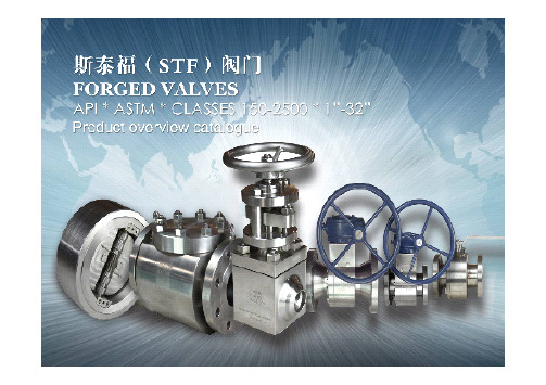
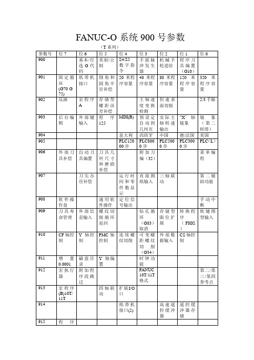
STF900系列产品规格与选型(中文)
- 格式:pdf
- 大小:491.64 KB
- 文档页数:11

ST风机方案1. 简介ST风机是一种高效的风机产品,具有高性能、低噪音和节能等特点。
本文档将介绍ST风机的方案,包括风机的工作原理、技术规格、特点和应用领域等内容。
2. 工作原理ST风机采用离心风叶设计,通过电动机的驱动和内部的风叶高速旋转,产生强劲的气流。
风机的进风口会将空气吸入,而出风口将空气排出。
风叶的旋转会对空气产生动力作用,从而形成气流。
3. 技术规格ST风机拥有以下技术规格:•电源:220V/50Hz•功率:500W•风量:1000m³/h•噪音:低于60dB•材质:聚合物材料•尺寸:500mm x 500mm x 200mm•重量:10kg4. 特点ST风机拥有以下特点:•高性能:ST风机配备强力电动机和优质风叶,能够产生强劲的气流,有效降低室内温度。
•低噪音:采用噪音减震技术和低噪音电机,使ST风机运行时噪音低于60dB,不会影响室内安静环境。
•节能:ST风机采用高效电机和优化的风叶设计,能够最大程度地降低能耗。
•轻便易携:ST风机体积小巧,重量轻,便于携带和安装,适用于各种场景。
5. 应用领域ST风机适用于以下场景:•家庭使用:ST风机可以有效降低室内温度,提供舒适的生活环境。
•商业场所:商场、餐厅、办公室等场所可以使用ST风机来改善空气流通和降低温度,提升顾客体验。
•工厂车间:ST风机可以在工厂车间中提供良好的通风和冷却效果,改善工作环境。
•公共场所:体育馆、会议厅等公共场所可以使用ST风机来调节室内温度,提供舒适的环境。
6. 安装与维护ST风机的安装和维护步骤如下:1.将ST风机放置在适合的位置,确保进风口没有障碍物。
2.将电源线插入电源插座。
3.风机正常运行后,可以通过控制面板或遥控器来调节风速。
4.定期清洁风机的进风口和出风口,以保持良好的通风效果。
5.如遇故障或异常情况,应立即停止使用并联系售后服务部门进行维修。
7. 常见问题解答7.1 ST风机是否可以调节风速?是的,ST风机配备了多档风速调节功能,可以根据需要调节风速。

1/11April 2003STP9NK90Z -STF9NK90ZSTW9NK90ZN-CHANNEL 900V -1.1Ω-8A TO-220/TO-220FP/TO-247Zener-Protected SuperMESH™Power MOSFETs TYPICAL R DS (on)=1.1Ωs EXTREMELY HIGH dv/dt CAPABILITY s 100%AVALANCHE TESTED s GATE CHARGE MINIMIZEDs VERY LOW INTRINSIC CAPACITANCES sVERY GOOD MANUFACTURING REPEATIBILITYDESCRIPTIONThe SuperMESH™series is obtained through an extreme optimization of ST’s well established strip-based PowerMESH™layout.In addition to pushing on-resistance significantly down,special care is tak-en to ensure a very good dv/dt capability for the most demanding applications.Such series comple-ments ST full range of high voltage MOSFET s in-cluding revolutionary MDmesh™products.APPLICATIONSs HIGH CURRENT,HIGH SPEED SWITCHING s SWITCH MODE POWER SUPPLIESs DC-AC CONVERTERS FOR WELDING,UPS AND MOTOR DRIVEORDERING INFORMATIONTYPE V DSS R DS(on)I D Pw STP9NK90Z STF9NK90Z STW9NK90Z900V 900V 900V<1.3Ω<1.3Ω<1.3Ω8A 8A 8A160W 40W 160WSALES TYPE MARKING PACKAGE PACKAGINGSTP9NK90Z P9NK90Z TO-220TUBE STF9NK90Z F9NK90Z TO-220FP TUBE STW9NK90ZW9NK90ZTO-247TUBESTP9NK90Z -STF9NK90Z -STW9NK90Z2/11ABSOLUTE MAXIMUM RATINGS( )Pulse width limited by safe operating area(1)I SD ≤8A,di/dt ≤200A/µs,V DD ≤V (BR)DSS ,T j ≤T JMAX.(*)Limited only by maximum temperature allowedTHERMAL DATAAVALANCHE CHARACTERISTICSGATE-SOURCE ZENER DIODEPROTECTION FEATURES OF GATE-TO-SOURCE ZENER DIODESThe built-in back-to-back Zener diodes have specifically been designed to enhance not only the device’s ESD capability,but also to make them safely absorb possible voltage transients that may occasionally be applied from gate to source.In this respect the Zener voltage is appropriate to achieve an efficient and cost-effective intervention to protect the device’s integrity.These integrated Zener diodes thus avoid the usage of external components.Symbol ParameterValueUnit STP9NK90ZSTF9NK90ZSTW9NK90ZV DS Drain-source Voltage (V GS =0)900V V DGR Drain-gate Voltage (R GS =20k Ω)900V V GS Gate-source Voltage±30VI D Drain Current (continuous)at T C =25°C 88(*)8A I D Drain Current (continuous)at T C =100°C 55(*)5A I DM ( )Drain Current (pulsed)3232(*)32A P TOT Total Dissipation at T C =25°C 16040160W Derating Factor1.280.32 1.28W/°C V ESD(G-S)Gate source ESD(HBM-C=100pF,R=1.5K Ω)4KV dv/dt (1)Peak Diode Recovery voltage slope 4.5V/nsV ISO Insulation Withstand Voltage (DC)-2500-V T j T stgOperating Junction Temperature Storage Temperature-55to 150-55to 150°C °CTO-220TO-220FPTO-247Rthj-case Thermal Resistance Junction-case Max 0.783.10.78°C/W Rthj-ambThermal Resistance Junction-ambient Max62.550°C/W T lMaximum Lead Temperature For Soldering Purpose300°CSymbol ParameterMax ValueUnit I AR Avalanche Current,Repetitive or Not-Repetitive (pulse width limited by T j max)8A E ASSingle Pulse Avalanche Energy(starting T j =25°C,I D =I AR ,V DD =50V)300mJSymbol ParameterTest ConditionsMin.Typ.Max.Unit BV GSOGate-Source Breakdown VoltageIgs=±1mA (Open Drain)30V3/11STP9NK90Z -STF9NK90Z -STW9NK90ZELECTRICAL CHARACTERISTICS (T CASE =25°C UNLESS OTHERWISE SPECIFIED)ON/OFFDYNAMICSWITCHING ONSWITCHING OFFSOURCE DRAIN DIODENote: 1.Pulsed:Pulse duration =300µs,duty cycle 1.5%.2.Pulse width limited by safe operating area.3.C oss eq.is defined as a constant equivalent capacitance giving the same charging time as C oss when V DS increases from 0to 80%V DSS .Symbol ParameterTest ConditionsMin.Typ.Max.Unit V (BR)DSS Drain-sourceBreakdown Voltage I D =1mA,V GS =0900V I DSS Zero Gate VoltageDrain Current (V GS =0)V DS =Max RatingV DS =Max Rating,T C =125°C 150µA µA I GSS Gate-body Leakage Current (V DS =0)V GS =±20V±10µA V GS(th)Gate Threshold Voltage V DS =V GS ,I D =100µA 33.754.5V R DS(on)Static Drain-source On ResistanceV GS =10V,I D =3.6A1.11.3ΩSymbol ParameterTest ConditionsMin.Typ.Max.Unit g fs (1)Forward Transconductance V DS =15V ,I D =3.6A5.75S C iss C oss C rss Input Capacitance Output Capacitance Reverse Transfer Capacitance V DS =25V,f =1MHz,V GS =0211519040pF pF pF C oss eq.(3)Equivalent Output CapacitanceV GS =0V,V DS =0V to 720V115pFSymbol ParameterTest ConditionsMin.Typ.Max.Unit t d(on)t r Turn-on Delay Time Rise TimeV DD =450V,I D =4A R G =4.7ΩV GS =10V(Resistive Load see,Figure 3)2213ns ns Q g Q gs Q gdTotal Gate Charge Gate-Source Charge Gate-Drain ChargeV DD =720V,I D =8A,V GS =10V721438100nC nC nCSymbol ParameterTest ConditionsMin.Typ.Max.Unit t d(off)t f Turn-off Delay Time Fall TimeV DD =450V,I D =4A R G =4.7ΩV GS =10V(Resistive Load see,Figure 3)5528ns ns t r(Voff)t f t cOff-voltage Rise Time Fall TimeCross-over TimeV DD =720V,I D =8A,R G =4.7Ω,V GS =10V(Inductive Load see,Figure 5)531122ns ns nsSymbol ParameterTest ConditionsMin.Typ.Max.Unit I SD I SDM (2)Source-drain CurrentSource-drain Current (pulsed)832A A V SD (1)Forward On Voltage I SD =8A,V GS =0 1.6V t rr Q rr I RRMReverse Recovery Time Reverse Recovery Charge Reverse Recovery CurrentI SD =8A,di/dt =100A/µs V DD =50V,T j =150°C (see test circuit,Figure 5)9501021ns µC ASTP9NK90Z -STF9NK90Z -STW9NK90Z4/11Safe Operating Area For TO-2475/11STP9NK90Z -STF9NK90Z -STW9NK90ZStatic Drain-source On ResistanceTransferCharacteristicsTransconductanceSTP9NK90Z -STF9NK90Z -STW9NK90Z6/11Normalized BVDSS vs TemperatureSource-drain Diode Forward Characteristics7/11STP9NK90Z -STF9NK90Z -STW9NK90ZFig.5:Test Circuit For Inductive Load Switching And Diode Recovery TimesFig.4:Gate Charge test CircuitFig.2:Unclamped Inductive WaveformFig.1:Unclamped Inductive Load TestCircuitFig.3:Switching Times Test Circuit For ResistiveLoadSTP9NK90Z-STF9NK90Z-STW9NK90Z8/11STP9NK90Z-STF9NK90Z-STW9NK90Z9/11STP9NK90Z-STF9NK90Z-STW9NK90Z10/11元器件交易网STP9NK90Z-STF9NK90Z-STW9NK90Z Information furnished is believed to be accurate and reliable. However, STMicroelectronics assumes no responsibility for theconsequences of use of such information nor for any infringement of patents or other rights of third parties which may result fromits use. No license is granted by implication or otherwise under any patent or patent rights of STMicroelectronics. Specificationsmentioned in this publication are subject to change without notice. This publication supersedes and replaces all informationpreviously supplied. STMicroelectronics products are not authorized for use as critical components in life support devices orsystems without express written approval of STMicroelectronics.© The ST logo is a registered trademark of STMicroelectronics© 2003 STMicroelectronics - Printed in Italy - All Rights ReservedSTMicroelectronics GROUP OF COMPANIESAustralia - Brazil - Canada - China - Finland - France - Germany - Hong Kong - India - Israel - Italy - Japan - Malaysia - Malta - MoroccoSingapore - Spain - Sweden - Switzerland - United Kingdom - United States.© 11/11。
AI...AI-TWIN...订货号根据DIN VDE0110:1989-01标准确定电器间隙和爬电距离VDE标准DIN VDE0110采纳了IEC标准IEC664/664A的实质性内容,以实现下述目标:从要承受的绝缘负荷出发来选所需要的绝缘强度,以此来确定所需的最小绝缘距离。
这一基本标准适用于这样一些情况,即仪器制造标准上没有有关确定电气间隙和爬电距离的规定。
若仪器制造标准上有相应的规定说明,则以仪器制造标准为准。
绝缘配合绝缘配合即在考虑器件的实际运用场合和环境条件的前提下确定器件应具备的绝缘特性。
这一方面涉及到与电气间隙有关的可能出现的过电压和过电压保护装置的特性值,另一方面涉及到与爬电距离有关的工作电压、会降低器件绝缘特性的直接周围环境和防污染保护措施。
因此电气间隙的大小要根据设备可能出现的外部的或内部的最大过电压来确定。
在不同场合使用器件或运用过电压保护装置时所出现的外部过电压大小各不相同。
因此将过电压按不同的使用场合分为l至lV四个等级。
在每个过电压等级中,根据所使用的配电网的额定电压的大小,确定相应的脉冲耐受电压值。
根据电场的均匀性情况(情况A-非均匀电场,情况B-均匀电场)从表2a(最小电气间隙)中找到最小电气间隙值。
情况A所确定的电气间隙可在任何情况下承受相应的脉冲耐受电压,这就是说根据A确定电气间隙尺寸的器件不需再做检验就可直接使用。
根据情况B确定的电气间隙值是理想条件下的电气间隙值。
介于情况A和情况B之间的电气间隙值需要通过做脉冲耐受电压实验来证实。
在确定电气间隙和爬电距离时通过将污染程度分为4个等级而将污染对绝缘特性的影响考虑在内。
爬电距离的确定基础是从供电电网的额定电压推导出来的基准电压。
由表4可知如何根据基准电压,污染等级来确定最小爬电距离值。
若在产品说明中无特殊说明,则本产品样本中所列产品的电气间隙和爬电距离均按标准DIN VDE0110:1989-01及过电压等级Ⅲ和污染等级3确定。
1
5
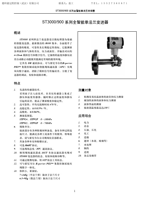
ST900系列工业型压力变送器
ST900系列压力变送器是珠海赛思特仪表设备有限公司研制开发的工业型压力变送器。
采用美国进口的高性能隔离式扩散硅压力传感器及电子集成电路技术制作而成。
高性能的敏感元件和先进可靠的信号处理技术使该产品具有高准确度、高长期稳定性、耐腐蚀、过载能力高、卓越的性能价格比等特点,同时具有防爆可选功能。
准确度等级:0.1%或
0.25%
量程比:额定量程内 5:
1
主要技术数据
~~~
~
环境温度范围:一般变送器-25℃ +80℃;防爆型-20℃ +70℃
贮藏温度:-40 +100℃电气外壳为铝合金,表面喷塑
电磁兼容/射频干扰:10V/m
外磁场强度:400A/m <抗振动:25g/20 500Hz 抗冲击:50g/10mS 外壳防护:IP65
环境湿度范围:0 100%/RH
,无冷凝结构材料:过程连接件为316不锈钢;
与介质接触密封圈为氟橡胶~
~
~~
2。
Features and Benefits Data SheetField ITFB900-S*4 Fieldbus BarrierFunctionFieldbus distributor with four individually short-circuit currentlimited outputs, intrinsically safe (EEx ia IIC) in accordance toFISCO and EntityDevice variantsFB900-SA4Aluminium field housing for Fieldbus Barrier with fourintrinsically safe outputs EEx ia, trunk EEx e, plastic cableglandFB900-SB4Stainless steel field housing for Fieldbus Barrier with fourintrinsically safe outputs EEx ia, trunk EEx e, stainlesssteel cable glandFB900-SR4Fieldbus Barrier without field housing, for mounting incabinet on DIN rail, four intrinsically safe outputs EEx ia,trunk EExeFB900-SA4FB900-SR4■Power supply of fieldbus segments according to IEC 61158-2■High power for general purpose or intrinsically safe topologies withFieldbus Barrier■High power in the field due to Ex e/ Ex i power feed concept■Connection of fieldbus trunk in increased safety EEx e■Installation in zone 1■Variants for cabinet installation on DIN mounting rail■Different housing and cableconnection variants for installationin the field■Switchable integrated fieldbus terminator■Efficient shielding concept due to electrical isolation between thefieldbus trunk and the intrinsicallysafe outputsField IT FB 900-S*4 Fieldbus Barrier23BDD011866R101FunctionalityGeneralIn FOUNDATION Fieldbus H1 or PROFIBUS PA topologies for explosion hazardous environments, the Fieldbus Barrier combines three essential functions:■distribution of the trunk line to up to four branch lines for fieldbus devices■supply of the connected devices in the explosion protection method "intrinsic safety" (EEx ia IIC)■protection of the trunk against negative influences due to short circuit current limitation for each branch lineEach output allows the connection of an intrinsically safe field device with a power consumption of up to 40mA. Each output cable can run up to 120m without the need for termination.The trunk connections are designed in protection type "increased safety" (EEx e) and thus allow a high supply current in the fieldbus segment. Several Fieldbus Barrier can be daisy-chained on one trunk. Switchable fieldbus terminators are integrated.For the interconnection of fieldbus devices (with consideration of the technical data of the FB 900-S*4) Layout Tools are available (price list of the product line 63, Fieldbus and Tools):■FOUNDATION Fieldbus Layout Tool DTE100, 3KDE633517■PROFIBUS Layout Tool DTD100, 3KDE633414For installation and commissioning of the Fieldbus Barrier please refer to the operating instructions 3BDD011862.ConnectionField IT FB 900-S*4 Fieldbus Barrier3BDD011866R1013Technical DataFieldbus interfaceMain cable (Trunk)Connection input (T runk IN): terminals 3+, 4-, 5s output (Trunk OUT): terminals 7-, 8+, 6s Rated voltage 16 ... 32 V DCRated current25 mA ... 22 mA (without load)121 mA ... 74mA (at 20 mA load per input) 230 mA ... 125 mA (at 40 mA load per input)255 mA ... 135 mA (short-circuit on all outputs)Number of Fieldbus Barriers max. 4 devices per segmentOutputs Connectionoutput 1: terminals 10+, 11-, 12S shield; output 2: terminals 13+, 14-, 15S shield; output 3: terminals 16+, 17-, 18S shield; output 4: terminals 19+, 20-, 21S shield Rated voltage ≥ 10 V at 40 mA Rated current ≤ 40 mA Short-circuit current ≤ 50 mATerminating impedance100 Ω switchable onIndicators/operating meansLED voltage Fieldbus green: on, bus voltage existent LED state outputs red flashing: short-circuitElectrical isolationMain wire/outputs isolation is not affected by interference according to EN 50020, voltage peak value 375 V Directive conformityElectromagnetic compatibilityDirective 89/336/EC EN 61326ConformityElectromagnetic compatibilityNAMUR NE 21Protection degree IEC/EN 60529Fieldbus standard IEC 61158-2Climatic conditions DIN IEC 721Ambient conditionsAmbient temperaturesee table 2Storage temperature -40 ... 85 °C (233 ... 358 K)Relative humidity < 95 % non-condensing Degree of soiling max. 2, according to IEC 60664Mechanical specificationsConnection type see table 2Core cross-section up to 2.5 mm 2Cable diameter see table 3Cable glandsee table 2Housing see figuresHousing material FB 900-SR4PA 6.6FB 900-SA4ALSI12 (Cu) DIN1725 (Si 1,2%), anodised FB 900-SB4 1.4404 (S316L)Mountingsee table 4Field IT FB 900-S*4 Fieldbus Barrier43BDD011866R101Table 1: Connection of terminalsTable 2: Variations of cable connections, housing types and temperature rangesTable 3: Cable diameter depending on cable glandData for application inconjunction withhazardous areas EC-T ype Examination CertificatePTB 05 ATEX 2033Group, category, type of protection, temperature classification ¬ II 2 (1G/D) G EEx me [ia] IIC T4Main cable (Trunk)Safety maximum voltage U m 253 V AC OutputsVoltageU o 15.75 V Current I o 248 mA PowerP o 975 mW Directive conformityDirective 94/9 ECEN 50014, EN 50019, EN 50020, EN 50028Terminals Function 10+, 13+, 16+, 19+Output EEx ia +11-, 14-, 17-, 20-Output EEx ia -12s, 15s, 18s, 21s Output shield 3+T runk IN, EEx e +4-T runk IN, EEx e -5s T runk IN, shield 7-T runk OUT, EEx e -8+T runk OUT, EEx e +6s T runk OUT, shield1B Outputs, shield bridge (delivery status)2B T runkPAPotential equalization, shield bridge (delivery status)The terminals 5s and 6s are connected internally with terminal 2B.The terminals 12s, 15s, 18s and 21s are connected internally with terminal 1B.The terminal PA is connected to the external earthing point (versions with field housing only).Changing the bridge from 1B – PA to 1B – 2B changes the shielding concept from "capacitive grounding" to "hard grounding".Device variants Type of cable connection Height (mm)SW1 (mm)SW2 (mm)Temperature range(°C)FB 900-SA4Terminals, cable glands plastic X = 1402024-30 ... 70FB 900-SB4Terminals, cable glands stainless steel Y = 2002224-40 ... 70FB 900-SR4Terminals–––-40 (70)Device variants Output cable diameter (mm)Trunk cable diameter (mm)FB 900-SA4 5 ... 107 ... 12FB 900-SB45 (10)7 (12)Field IT FB900-S*4 Fieldbus Barrier Table 4: Mechanical specificationsDevice variants Protection degree Mass (g)MountingFB900-SA4IP673350Panel mountingFB900-SB4IP662500Panel mountingFB900-SR4IP201050Mounting on DIN rail in cabinet Dimensions3BDD011866R1015For more information on Field IT ,**************************.comFor the latest information on ABB visit us on the World Wide Web at Field IT FB 900-S*4 Fieldbus BarrierAutomation T echnologies Mannheim, Germanyhttp://www.abb.de/controlsystemsemail:*********************************.comAutomation Technologies Wickliffe, Ohio, USA/controlsystems email:****************************.com Automation Technologies Västerås, Sweden/controlsystems email:************************.com 3BDD011866R101 Printed in Germany June 2005Copyright © 2005 by ABB, All Rights Reserved ® Registered Trademark of ABB ™ Trademark of ABB。