LT3478中文资料
- 格式:pdf
- 大小:283.79 KB
- 文档页数:24

Document number: MC34712Rev. 4.0, 5/2007Freescale Semiconductor Advance Information* This document contains certain information on a new product.Specifications and information herein are subject to change without notice.© Freescale Semiconductor, Inc., 2007. All rights reserved.3.0 A 1.0 MHz Fully Integrated DDR Switch-Mode Power SupplyThe 34712 is a highly integrated, space efficient, low cost, single synchronous buck switching regulator with integrated N-channel power MOSFETs. It is a high performance point-of-load (PoL) power supply with the ability to track an external reference voltage.Its high efficient 3.0 A sink and source capability combined with its voltage tracking/sequencing ability and tight output regulation, makes it ideal to provide the termination voltage (V TT ) for modern data buses such as Double-Data-Rate (DDR) memory buses. It also provides a buffered output reference voltage (V REF ) to the memory chipset The 34712 offers the designer the flexibility of many control,supervisory, and protection functions to allow for easy implementation of complex designs. It is housed in a Pb-Free, thermally enhanced, and space efficient 24-Pin Exposed Pad QFN.Features•45 m Ω Integrated N-Channel Power MOSFETs •Input Voltage Operating Range from 3.0 V to 6.0 V•±1 % Accurate Output Voltage, Ranging from 0.7 V to 1.35 V •±1 % Accurate Buffered Reference Output Voltage•Programmable Switching Frequency Range from 200 kHz to 1.0 MHz with a default of 1.0 MHz•Over Current Limit and Short Circuit Protection •Thermal Shutdown•Output Overvoltage and Undervoltage Detection •Active Low Power Good Output Signal •Active Low Standby and Shutdown Inputs•Pb-Free Packaging Designated by Suffix Code EP.Figure 1. 34712 Simplified Application DiagramSWITCH-MODE POWER SUPPLYEP SUFFIX 98ARL10577D 24-PIN QFN34712ORDERING INFORMATIONDevice Temperature Range (T A )Package MC34712EP/R2-40 to 85°C24 QFNV INMCUPVINVREFINVIN VDDI FREQ GND SDSTBYBOOTSWVOUT INV COMP VREFOUTPGND PGDDR MEMORY CONTROLER34712V DDQDDR MEMORY CHIPSET V INV REFV TTV DDQV DDQMEMORY BUSTERMINATING RESISTORS(3.0V TO 6.0V)INTERNAL BLOCK DIAGRAMINTERNAL BLOCK DIAGRAMFigure 2. 34712 Simplified Internal Block Diagram34712Analog Integrated Circuit Device DataAnalog Integrated Circuit Device Data 34712PIN CONNECTIONSPIN CONNECTIONSFigure 3. 34712 Pin ConnectionsTable 1. 34712 Pin DefinitionsA functional description of each pin can be found in the Functional Pin Description section beginning onpage 10.Pin NumberPin Name Pin Function Formal Name Definition1GND Ground Signal GroundAnalog signal ground of IC2FREQ Passive Frequency Adjustment Buck converter switching frequency adjustment pin3NC None No Connect No internal connections to this pin4PG Output Power Good Active-low (open drain) power-good status reporting pin 5STBY Input Standby Standby mode input control pin 6SDInput Shutdown Shutdown mode input control pin 7VREFIN Input Voltage-Tracking-Reference Input Voltage-Tracking-Reference voltage input8VREFOUTOutput Reference VoltageOutput Buffered output equal to 1/2 of voltage-tracking reference 9COMPPassive Compensation Buck converter external compensation network pin 10INV Input Error Amplifier Inverting Input Buck converter error amplifier inverting input pin11VOUT Output Output Voltage Discharge FET Discharge FET drain connection (connect to buck converter output capacitors)12,13,14PGND Ground Power Ground Ground return for buck converter and discharge FET 15,16,17SW Power Switching Node Buck converter power switching node 18,19,20PVIN Supply Power-Circuit SupplyInputBuck converter main supply voltage input21BOOTPassiveBootstrapBootstrap switching node (connect to bootstrap capacitor)GND FREQ STBY PG NC SDV R E F I NC O M PI N VV O U TP G N DSW P V I NB O O TV I NV D D IV R E F O U TPGND PGNDSW SWPVIN P V I NV I NAnalog Integrated Circuit Device Data34712PIN CONNECTIONS22,23VINSupply Logic-Circuit SupplyInput Logic circuits supply voltage input24VDDIPassiveInternal Voltage RegulatorInternal Vdd Regulator (connect filter capacitor to this pin)Table 1. 34712 Pin Definitions (continued)A functional description of each pin can be found in the Functional Pin Description section beginning on page 10.Pin NumberPin NamePin FunctionFormal Name DefinitionAnalog Integrated Circuit Device Data 34712ELECTRICAL CHARACTERISTICSMAXIMUM RATINGSELECTRICAL CHARACTERISTICSMAXIMUM RATINGSTable 2. Maximum RatingsAll voltages are with respect to ground unless otherwise noted. Exceeding these ratings may cause a malfunction or permanent damage to the device.RatingsSymbolValueUnitELECTRICAL RATINGS Input Supply Voltage (VIN) PinV IN -0.3 to 7.0V High-Side MOSFET Drain Voltage (PVIN) Pin PV IN -0.3 to 7.0V Switching Node (SW) PinV SW -0.3 to 7.5V BOOT Pin (Referenced to SW Pin)V BOOT - V SW-0.3 to 7.5V PG, VOUT, SD, and STBY Pins--0.3 to 7.0V VDDI, FREQ, INV, COMP, VREFIN, and VREFOUT Pins --0.3 to 3.0V Continuous Output Current (1)I OUT±3.0AESD Voltage (2)Human Body Model Device Charge Model (CDM)V ESD1V ESD3±2000±750VTHERMAL RATINGSOperating Ambient Temperature (3)T A -40 to 85°C Storage TemperatureT STG -65 to +150°C Peak Package Reflow Temperature During Reflow (4), (5)T PPRT Note 5°C Maximum Junction Temperature T J(MAX)+150°C Power Dissipation (T A = 85 °C) (6)P D2.9WNotes1.Continuous output current capability so long as T J is ≤ T J(MAX).2.ESD1 testing is performed in accordance with the Human Body Model (C ZAP = 100 pF, R ZAP = 1500 Ω), ESD3 testing is performed inaccordance with the Charge Device Model (CDM).3.The limiting factor is junction temperature, taking into account power dissipation, thermal resistance, and heatsinking.4.Pin soldering temperature limit is for 10 seconds maximum duration. Not designed for immersion soldering. Exceeding these limits maycause malfunction or permanent damage to the device.5.Freescale’s Package Reflow capability meets Pb-free requirements for JEDEC standard J-STD-020C. For Peak Package ReflowTemperature and Moisture Sensitivity Levels (MSL),Go to , search by part number [e.g. remove prefixes/suffixes and enter the core ID to view all orderable parts. (i.e. MC33xxxD enter 33xxx), and review parametrics.6.Maximum power dissipation at indicated ambient temperature.Analog Integrated Circuit Device Data34712ELECTRICAL CHARACTERISTICS MAXIMUM RATINGSTHERMAL RESISTANCE (7)Thermal Resistance, Junction to Ambient, Single-Layer Board (1s) (8)R θJA 139°C/W Thermal Resistance, Junction to Ambient, Four-Layer Board (2s2p) (9)R θJMA 43°C/W Thermal Resistance, Junction to Board (10)R θJB22°C/WNotes7.The PVIN, SW, and GND pins comprise the main heat conduction paths.8.Per SEMI G38-87 and JEDEC JESD51-2 with the single-layer board (JESD51-3) horizontal.9.Per JEDEC JESD51-6 with the board (JESD51-7) horizontal. There are no thermal vias connecting the package to the two planes in theboard.10.Thermal resistance between the device and the printed circuit board per JEDEC JESD51-8. Board temperature is measured on the topsurface of the board near the package.Table 2. Maximum Ratings (continued)All voltages are with respect to ground unless otherwise noted. Exceeding these ratings may cause a malfunction or permanent damage to the device.RatingsSymbolValueUnitAnalog Integrated Circuit Device Data 34712ELECTRICAL CHARACTERISTICSSTATIC ELECTRICAL CHARACTERISTICSSTATIC ELECTRICAL CHARACTERISTICSTable 3. Static Electrical CharacteristicsCharacteristics noted under conditions 3.0 V ≤ V IN ≤ 6.0 V, - 40°C ≤ T A ≤ 85°C, GND = 0 V unless otherwise noted. Typical values noted reflect the approximate parameter means at T A = 25°C under nominal conditions unless otherwise noted.CharacteristicSymbolMinTypMaxUnitIC INPUT SUPPLY VOLTAGE (VIN) Input Supply Voltage Operating Range V IN 3.0- 6.0VInput DC Supply Current (11)Normal Mode: SD = 1 & STBY = 1, Unloaded Outputs I IN --25mAInput DC Supply Current (11)Standby Mode, SD = 1 & STBY = 0I INQ --15mAInput DC Supply Current (11)Shutdown Mode, SD = 0 & STBY = XI INOFF--100µAINTERNAL SUPPLY VOLTAGE OUTPUT (VDDI)Internal Supply Voltage RangeV DDI2.352.52.65VBUCK CONVERTER (PVIN, SW, GND, BOOT, INV, COMP)High-side MOSFET Drain Voltage Range P VIN 2.5- 6.0V Output Voltage Adjustment Range (12)V OUT 0.7- 1.35V Output Voltage Accuracy (12), (13), (14)--1.0- 1.0%Line Regulation (12)Normal Operation, V IN = 3.0 V to 6.0 V, I OUT = ±3.0 A REG LN -1.0- 1.0%Load Regulation (12)Normal Operation, I OUT = -3.0 A to 3.0 AREG LD-1.0- 1.0%Error Amplifier Common Mode Voltage Range (12), (15)V REF0.0- 1.35V Output Undervoltage Threshold V UVR -1.5--8.0%Output Overvoltage Threshold V OVR 1.5-8.0%Continuous Output CurrentI OUT -3.0- 3.0A Over Current Limit, Sinking and Sourcing I LIM - 4.0-A Short Circuit Current Limit (Sourcing and Sinking)I SHORT -6.5-AHigh-Side N-CH Power MOSFET (M3) R DS(ON) (12)I OUT = 1.0 A, V BOOT - V SW = 3.3 VR DS(ON)HS 10-45m ΩLow-Side N-CH Power MOSFET (M4) R DS(ON) (12)I OUT = 1.0 A, V IN = 3.3 V R DS(ON)LS10-45m ΩNotes 11.See section “MODES OF OPERATION”, page 14 has a detailed description of the different operating modes of the 3471212.Design information only, this parameter is not production tested.13.±1% is assured at room temperature.14.Overall output accuracy is directly affected by the accuracy of the external feedback network, 1% feedback resistors are recommended.15.The 1% output voltage regulation is only guaranteed for a common mode voltage range greater than or equal to 0.7V at room temperature.Analog Integrated Circuit Device Data34712ELECTRICAL CHARACTERISTICSSTATIC ELECTRICAL CHARACTERISTICSM2 R DS(ON)(V IN = 3.3 V, M2 is on)R DS(ON)M21.5- 4.0ΩPVIN Pin Leakage Current (Standby and Shutdown Modes)I PVIN -10-10µA INV Pin Leakage Current I INV -1.0- 1.0µA Thermal Shutdown Threshold (16)T SDFET -170-°C Thermal Shutdown Hysteresis (16)T SDHYFET-25-°COSCILLATOR (FREQ)Oscillator Frequency Adjusting Reference Voltage Range V FREQ0.0-V DDIVTRACKING (VREFIN, VREFOUT, VOUT)VREFIN External Reference Voltage Range (16)V REFIN 0.0- 2.7V VREFOUT Buffered Reference Voltage Range V REFOUT0.0- 1.35V VREFOUT Buffered Reference Voltage Accuracy (17)--1.0- 1.0%VREFOUT Buffered Reference Voltage Current Capability I REFOUT 0.0-8.0mA VREFOUT Buffered Reference Voltage Over Current Limit I REFOUTLIM -11-mA VREFOUT Total Discharge Resistance (16)R TDR(M6)-50-ΩVOUT Total Discharge Resistance (16)R TDR(M5)-50-ΩVOUT Pin Leakage Current (Standby Mode, V OUT = 3.6 V)I VOUTLKG-1.0- 1.0µACONTROL AND SUPERVISORY (STBY, SD, PG)STBY High Level Input Voltage V STBYHI 2.0--V STBY Low Level Input Voltage V STBYLO --0.4V STBY Pin Internal Pull Up Resistor R STBYUP 1.0- 2.0M ΩSD High Level Input Voltage V SDHI 2.0--V SD Low Level Input Voltage V SDLO --0.4V SD Pin Internal Pull Up Resistor R SDUP 1.0- 2.0M ΩPG Low Level Output Voltage (I PG = 3.0 mA)V PGLO --0.4VPG Pin Leakage Current (M1 is off, Pulled up to VIN)I PGLKG-1.0- 1.0µANotes16.Design information only, this parameter is not production tested.17.The 1 % accuracy is only guaranteed for V REFOUT greater than or equal to 0.7 V at room temperature.Table 3. Static Electrical CharacteristicsCharacteristics noted under conditions 3.0 V ≤ V IN ≤ 6.0 V, - 40°C ≤ T A ≤ 85°C, GND = 0 V unless otherwise noted. Typical values noted reflect the approximate parameter means at T A = 25°C under nominal conditions unless otherwise noted.CharacteristicSymbol Min Typ Max UnitAnalog Integrated Circuit Device Data 34712ELECTRICAL CHARACTERISTICSDYNAMIC ELECTRICAL CHARACTERISTICSDYNAMIC ELECTRICAL CHARACTERISTICSTable 4. Dynamic Electrical CharacteristicsCharacteristics noted under conditions 3.0 V ≤ V IN ≤ 6.0 V, - 40°C ≤ T A ≤ 85°C, GND = 0 V unless otherwise noted. Typical values noted reflect the approximate parameter means at T A = 25°C under nominal conditions unless otherwise noted.CharacteristicSymbolMinTypMaxUnitBUCK CONVERTER (PVIN, SW, GND, BOOT)Switching Node (SW) Rise Time (19)(P VIN = 3.3 V, I OUT = ±3.0 A)t RISE -14-nsSwitching Node (SW) Fall Time (19)(P VIN = 3.3 V, I OUT = ±3.0 A)t FALL -20-nsSoft Start Duration (Normal Mode)t SS 1.3- 2.6ms Over Current Limit Timert LIM -10-ms Over Current Limit Retry Time-out Periodt TIMEOUT 80-120ms Output Undervoltage/Overvoltage Filter Delay Timer t FILTER5.0-25µsOSCILLATOR (FREQ)Oscillator Default Switching Frequency (18)(FREQ = GND)F SW - 1.0-MHz Oscillator Switching Frequency RangeF SW200-1000kHzCONTROL AND SUPERVISORY (STBY, SD, PG)PG Reset Delayt PGRESET 8.0-12ms Thermal Shutdown Retry Time-out Period (19)t TIMEOUT80-120msNotes18.Oscillator Frequency tolerance is ±10%.19.Design information only, this parameter is not production tested.Analog Integrated Circuit Device Data34712FUNCTIONAL DESCRIPTION INTRODUCTIONFUNCTIONAL DESCRIPTIONINTRODUCTIONIn modern microprocessor/memory applications, address commands and control lines require system level termination to a voltage (V TT ) equal to 1/2 the memory supply voltage (V DDQ ). Having the termination voltage at midpoint, the power supply insures symmetry for switching times. Also, areference voltage (V REF ) that is free of any noise or voltage variations is needed for the DDR SDRAM input receiver, V REF is also equal to 1/2 V DDQ . Varying the V REF voltage will effect the setup and hold time of the memory. To comply with DDR requirements and to obtain best performance, V TT and V REF need to be tightly regulated to track 1/2 V DDQ across voltage, temperature, and noise margins. V TT should track any variations in the DC V REF value (V TT = V REF +/- 40 mV), (See Figure 4) for a DDR system level diagram.The 34712 supplies the V TT and a buffered V REF output. To ensure compliance with DDR specifications, the V DDQ line is applied to the VREFIN pin and divided by 2 internally through a precision resistor divider. This internal voltage is then used as the reference voltage for the V TT output. The same internal voltage is also buffered to give the V REFvoltage at the VREFOUT pin for the application to use without the need for an external resistor divider. The 34712 provides the tight voltage regulation and power sequencing/tracking required along with handling the DDR peak transient current requirements. Buffering the V REF output helps its immunity against noise and load changes.The 34712 utilizes a voltage mode synchronous buck switching converter topology with integrated low R DS(ON) (45 m Ω) N-channel power MOSFETs to provide a V TT voltage with an accuracy of less than ±2.0 %. It has a programmable switching frequency that allows for flexibility and optimization over the operating conditions and can operate at up to1.0 MHz to significantly reduce the external components size and cost. The 34712 can sink and source up to 3.0 A ofcontinuous current. It provides protection against output over current, overvoltage, undervoltage, and overtemperature conditions. It also protects the system from short circuitevents. It incorporates a power-good output signal to alert the host when a fault occurs.For boards that support the Suspend-To-RAM (S3) and the Suspend-To-Disk (S5) states, the 34712 offers the STBY and the SD pins respectively. Pulling any of these pins low, puts the IC in the corresponding state.By integrating the control/supervisory circuitry along with the Power MOSFET switches for the buck converter into a space-efficient package, the 34712 offers a complete, small-size, cost-effective, and simple solution to satisfy the needs of DDR memory applications.Besides DDR memory termination, the 34712 can be used to supply termination for other active buses and graphics card memory. It can be used in Netcom/Telecom applications like servers. It can also be used in desktop motherboards, game consoles, set top boxes, and high end high definition TVs.Figure 4. DDR System Level DiagramFUNCTIONAL PIN DESCRIPTIONREFERENCE VOLTAGE INPUT (VREFIN)The 34712 will track 1/2 the voltage applied at this pin.REFERENCE VOLTAGE OUTPUT (VREFOUT)This is a buffered reference voltage output that is equal to 1/2 V REFIN . It has a 10.0 mA current drive capability. This output is used as the V REF voltage rail and should be filtered against any noise. Connect a 0.1 µF, 6 V low ESR ceramic filter capacitor between this pin and the GND pin andbetween this pin and V DDQ rail. V REFOUT is also used as the reference voltage for the buck converter error amplifier.FREQUENCY ADJUSTMENT INPUT (FREQ)The buck converter switching frequency can be adjusted by connecting this pin to an external resistor divider between VDDI and GND pins. The default switching frequency (FREQ pin connected to ground, GND) is set at 1.0 MHz.SIGNAL GROUND (GND)Analog ground of the IC. Internal analog signals are referenced to this pin voltage.V DDQV DDQV TTV REFBUSDDR Memory Controller DDR Memory Input ReceiverR SR TFUNCTIONAL DESCRIPTION FUNCTIONAL PIN DESCRIPTIONINTERNAL SUPPLY VOLTAGE OUTPUT (VDDI) This is the output of the internal bias voltage regulator. Connect a 1.0 µF, 6 V low ESR ceramic filter capacitor between this pin and the GND pin. Filtering any spikes on this output is essential to the internal circuitry stable operation.OUTPUT VOLTAGE DISCHARGE PATH (VOUT) Output voltage of the Buck Converter is connected to this pin. it only serves as the output discharge path once the SD signal is asserted.ERROR AMPLIFIER INVERTING INPUT (INV) Buck converter error amplifier inverting input. Connect the VTT voltage directly to this pin.COMPENSATION INPUT (COMP)Buck converter external compensation network connects to this pin. Use a type III compensation network.INPUT SUPPLY VOLTAGE (VIN)IC power supply input voltage. Input filtering is required for the device to operate properly.POWER GROUND (PGND)Buck converter and discharge MOSFETs power ground. It is the source of the buck converter low-side power MOSFET. SWITCHING NODE (SW)Buck converter switching node. This pin is connected to the output inductor.POWER INPUT VOLTAGE (PVIN)Buck converter power input voltage. This is the drain of the buck converter high-side power MOSFET. BOOTSTRAP INPUT (BOOT)Bootstrap capacitor input pin. Connect a capacitor (as discussed on page 19) between this pin and the SW pin to enhance the gate of the high-side Power MOSFET during switching.SHUTDOWN INPUT (SD)If this pin is tied to the GND pin, the device will be in Shutdown Mode. If left unconnected or tied to the VIN pin, the device will be in Normal Mode. The pin has an internal pull up of 1.5 MΩ. This input accepts the S5 (Suspend-To-Disk) control signal.STANDBY INPUT (STBY)If this pin is tied to the GND pin, the device will be in Standby Mode. If left unconnected or tied to the VIN pin, the device will be in Normal Mode. The pin has an internal pull up of 1.5 MΩ. This input accepts the S3 (Suspend-To-RAM) control signal.POWER GOOD OUTPUT SIGNAL (PG)This is an active low open drain output that is used to report the status of the device to a host. This output activates after a successful power up sequence and stays active as long as the device is in normal operation and is not experiencing any faults. This output activates after a 10 ms delay and must be pulled up by an external resistor to a supply voltage (e.g.,V IN.).FUNCTIONAL DESCRIPTIONFUNCTIONAL INTERNAL BLOCK DESCRIPTIONFUNCTIONAL INTERNAL BLOCK DESCRIPTIONFigure 5. 34712 Internal Block DiagramINTERNAL BIAS CIRCUITSThis block contains all circuits that provide the necessary supply voltages and bias currents for the internal circuitry. It consists of:•Internal Voltage Supply Regulator: This regulator supplies the V DDI voltage that is used to drive the digital/ analog internal circuits. It is equipped with a Power-On-Reset (POR) circuit that watches for the right regulation levels. External filtering is needed on the VDDI pin. This block will turn off during the shutdown mode.•Internal Bandgap Reference Voltage: This supplies the reference voltage to some of the internal circuitry.•Bias Circuit: This block generates the bias currents necessary to run all of the blocks in the IC. SYSTEM CONTROL AND LOGICThis block is the brain of the IC where the device processes data and reacts to it. Based on the status of the STBY and SD pins, the system control reacts accordingly and orders the device into the right status. It also takes inputs from all of the monitoring/protection circuits and initiates power up or power down commands. It communicates with the buck converter to manage the switching operation and protects it against any faults.OSCILLATORThis block generates the clock cycles necessary to run the IC digital blocks. It also generates the buck converter switching frequency. The switching frequency has a default value of 1.0 MHz and can be programmed by connecting a resistor divider to the FREQ pin, between VDDI and GND pins (See Figure 1).PROTECTION FUNCTIONSThis block contains the following circuits:•Over Current Limit and Short Circuit Detection: This block monitors the output of the buck converter for over current conditions and short circuit events and alerts the system control for further command.•Thermal Limit Detection: This block monitors the temperature of the device for overheating events. If the temperature rises above the thermal shutdownthreshold, this block will alert the system control forfurther commands.•Output Overvoltage and Undervoltage Monitoring: This block monitors the buck converter output voltage toensure it is within regulation boundaries. If not, thisblock alerts the system control for further commands.CONTROL AND SUPERVISORY FUNCTIONS This block is used to interface with an outside host. It contains the following circuits:•Standby Control Input: An outside host can put the 34712 device into standby mode (S3 or Suspend-To-RAM mode) by sending a logic “0” to the STBY pin.•Shutdown Control Input: An outside host can put the 34712 device into shutdown mode (S5 or Suspend-To-Disk mode) by sending a logic “0” to the SD pin.•Power Good Output Signal PG: The 34712 can communicate to an external host that a fault hasInternal Bias System ControlOscillator Circuits& LogicControl &Protection Tracking &SupervisoryFunctionsFunctionsSequencingBuck ConverterFUNCTIONAL DESCRIPTION FUNCTIONAL INTERNAL BLOCK DESCRIPTIONoccurred by releasing the drive on the PG pin high,allowing the signal/pin to be pulled high by the external pull-up resistor.TRACKING AND SEQUENCINGThis block allows the output of the 34712 to track 1/2 the voltage applied at the VREFIN pin. This allows the V REF and V TT voltages to track 1/2 V DDQ and assures that none of them will be higher than V DDQ at any point during normal operating conditions. For power down during a shutdown (S5) mode, the 34712 uses internal discharge MOSFETs (M5 and M6 on Figure 2) to discharge V TT and V REF respectively. These discharge MOSFETs are only active during shutdown mode. Using this block along with controlling the SD and STBY pins can offer the user power sequencing capabilities by controlling when to turn the 34712 outputs on or off.BUCK CONVERTERThis block provides the main function of the 34712: DC to DC conversion from an un-regulated input voltage to a regulated output voltage used by the loads for reliable operation. The buck converter is a high performance, fixed frequency (externally adjustable), synchronous buck PWM voltage-mode control. It drives integrated 45 mΩ N-channel power MOSFETs saving board space and enhancing efficiency. The switching regulator output voltage is adjustable with an accuracy of less than ±2.0 % to meet DDR requirements. Its output has the ability to track 1/2 the voltage applied at the VREFIN pin. The regulator's voltage control loop is compensated using a type III compensation network, with external components to allow for optimizing the loop compensation, for a wide range of operating conditions. A typical Bootstrap circuit with an internal PMOS switch is used to provide the voltage necessary to properly enhance the high-side MOSFET gate.The 34712 is designed to address DDR memory power supplies. The integrated converter has the ability to both sink and source up to 3.0 A of continuous current, making it suitable for bus termination power supplies.FUNCTIONAL DEVICE OPERATIONOPERATIONAL MODESFUNCTIONAL DEVICE OPERATIONOPERATIONAL MODESFigure 6. Operation Modes DiagramMODES OF OPERATIONThe 34712 has three primary modes of operation:Normal ModeIn normal mode, all functions and outputs are fully operational. To be in this mode, the V IN needs to be within its operating range, both Shutdown and Standby inputs are high, and no faults are present. This mode consumes the most amount of power.Standby ModeThis mode is predominantly used in Desktop memory solutions where the DDR supply is desired to be ACPI compliant (Advanced Configuration and Power Interface). When this mode is activated by pulling the STBY pin low, V TT is put in High Z state, I OUT = 0 A, and V REF stays active. This is the S3 state Suspend-To-Ram or Self Refresh mode and it is the lowest DRAM power state. In this mode, the DRAM will preserve the data. While in this mode, the 34712 consumes less power than in the normal mode, because the buck converter and most of the internal blocks are disabled.Shutdown ModeIn this mode, activated by pulling the SD pin low, the chip is in a shutdown state and the outputs are all disabled and discharged. This is the S4/S5 power state or Suspend-To-Disk state, where the DRAM will loose all of its data content (no power supplied to the DRAM). The reason to discharge the V TT and V REF lines is to ensure upon exiting, the Shutdown Mode that V TT and V REF are lower than V DDQ, otherwise V TT can remain floating high, and be higher than V DDQ upon powering up. In this mode, the 34712 consumes the least amount of power since almost all of the internal blocks are disabled.START-UP SEQUENCEWhen power is first applied, the 34712 checks the status of the SD and STBY pins. If the device is in a shutdown mode, no block will power up and the output will not attempt to ramp. If the device is in a standby mode, only the V DDI internal supply voltage and the bias currents are established and no further activities will occur. Once the SD and STBY pins are released to enable the device, the internal V DDI POR signal is also released. The rest of the internal blocks will be enabled。

新型高调光比LED驱动器设计大功率照明方案
LED照明解决方案广受欢迎的原因之一,是LED能通过简单的电流控制来获得很宽的调光范围,比如汽车仪表盘和飞机驾驶员座舱等环境照度可能非常低的应用场合就需要非常宽的PWM调光范围。
凌力尔特公司的
LT3478和LT3478-1是单芯片升压型DC/DC转换器,能在很宽的可设置范围内利用恒定电流来驱动高亮度LED。
除了可选的10:1模拟调光范围之外,LT3478和LT3478-1还具有3000:1的PWM调光范围,可以保持LED的色彩。
LT3478和LT3478-1的易用性很好,并具有旨在优化性能、可靠性、外形尺寸和总成本的可编程功能。
这些器件可工作在升压、降压和降升压型LED驱动器拓扑结构中。
它们所能提供的LED电流大小取决于拓扑结构,最高可达4A。
LT3478和LT3478-1是大功率LED应用(包括汽车和航空电子照明)的理想选择,它们采用16引脚耐热增强型TSSOP封装,具有E级或I级温度额定值。
图1:面向汽车TFT LED背光应用的升压型LED驱动电路。


元器件交易网IMPORTANT NOTICETexas Instruments and its subsidiaries (TI) reserve the right to make changes to their products or to discontinueany product or service without notice, and advise customers to obtain the latest version of relevant informationto verify, before placing orders, that information being relied on is current and complete. All products are soldsubject to the terms and conditions of sale supplied at the time of order acknowledgement, including thosepertaining to warranty, patent infringement, and limitation of liability.TI warrants performance of its semiconductor products to the specifications applicable at the time of sale inaccordance with TI’s standard warranty. Testing and other quality control techniques are utilized to the extentTI deems necessary to support this warranty. Specific testing of all parameters of each device is not necessarilyperformed, except those mandated by government requirements.CERTAIN APPLICATIONS USING SEMICONDUCTOR PRODUCTS MAY INVOLVE POTENTIAL RISKS OFDEATH, PERSONAL INJURY, OR SEVERE PROPERTY OR ENVIRONMENTAL DAMAGE (“CRITICALAPPLICATIONS”). TI SEMICONDUCTOR PRODUCTS ARE NOT DESIGNED, AUTHORIZED, ORWARRANTED TO BE SUITABLE FOR USE IN LIFE-SUPPORT DEVICES OR SYSTEMS OR OTHERCRITICAL APPLICATIONS. INCLUSION OF TI PRODUCTS IN SUCH APPLICATIONS IS UNDERSTOOD TOBE FULLY AT THE CUSTOMER’S RISK.In order to minimize risks associated with the customer’s applications, adequate design and operatingsafeguards must be provided by the customer to minimize inherent or procedural hazards.TI assumes no liability for applications assistance or customer product design. TI does not warrant or representthat any license, either express or implied, is granted under any patent right, copyright, mask work right, or otherintellectual property right of TI covering or relating to any combination, machine, or process in which suchsemiconductor products or services might be or are used. TI’s publication of information regarding any thirdparty’s products or services does not constitute TI’s approval, warranty or endorsement thereof.Copyright © 1998, Texas Instruments Incorporated。


13474fdThe L T ®3474/L T3474-1 are fi xed frequency step-down DC/DC converters designed to operate as constant-current sources. An internal sense resistor monitors the output current allowing accurate current regulation, ideal for driving high current LEDs. High output current accuracy is maintained over a wide current range, from 35mA to 1A, allowing a wide dimming range.Unique PWM circuitry allows a dimming range of 400:1, avoiding the color shift normally associated with LE D current dimming.The high switching frequency offers several advantages, permitting the use of small inductors and ceramic capaci-tors. Small inductors combined with the 16-lead TSSOP surface mount package save space and cost versus alternative solutions. The constant switching frequency combined with low-impedance ceramic capacitors result in low, predictable output ripple.With their wide input range of 4V to 36V , the L T3474/L T3474-1 regulate a broad array of power sources, from 5V logic rails to unregulated wall transformers, lead acid batteries and distributed power supplies. A current mode PWM architecture provides fast transient response and cycle-by-cycle current limiting. Frequency foldback and thermal shutdown provide additional protection.■Automotive and Avionic Lighting ■ Architectural Detail Lighting ■ Display Backlighting■ Constant Current SourcesnT rue Color PWM™ Delivers Constant Color with 400:1 Dimming Rangen Wide Input Range: 4V to 36V n Up to 1A LED Currentn Adjustable 200kHz–2MHz Switching Frequency n Adjustable Control of LED Current n Integrated Boost Dioden High Output Current Accuracy is Maintained Over a Wide Range from 35mA to 1An Open LED (L T3474) and Short-Circuit Protection n High Side Sense Allows Grounded Cathode Connectionn Uses Small Inductors and Ceramic Capacitors n L T3474-1 Drives LED Strings Up to 26Vn Compact 16-Lead TSSOP Thermally Enhanced Surface Mount PackageT YPICAL APPLICATIOND ESCRIPTION 1A LED DriverStep-Down 1A LED DriverL , LT, LTC and LTM are registered trademarks of Linear Technology Corporation.True Color PWM is a trademark of Linear Technology Corporation. All other trademarks are the property of their respective owners. Patent PendingF EATURESA PPLICATIONS Effi ciencyV IN 5V TO 36VLED CURRENT (mA)0E F F I C I E N C Y (%)70758060010003474 G0265605520040080085909523474fdP IN CONFIGURATIONA BSOLUTE MAXIMUM RATINGS V IN Pin ........................................................(–0.3V), 36V BIAS Pin ....................................................................25V BOOST Pin Voltage ...................................................51V BOOST above SW Pin ...............................................25V OUT , LED Pins (L T3474) ............................................15V OUT , LED Pins (L T3474-1) .........................................26V PWM Pin ...................................................................10V V ADJ Pin (6V)V C , REF, R T Pins ..........................................................3V SHDN Pin ...................................................................V IN BIAS Pin Current .........................................................1A Maximum Junction Temperature (Note 2).............125°C Operating Temperature Range (Note 3)L T3474E, L T3474E-1 ............................–40°C to 85°C L T3474I, L T3474I-1 ............................–40°C to 125°C Storage Temperature Range ...................–65°C to 150°C Lead Temperature (Soldering, 10 sec) ..................300°C(Note 1)ORDER INFORMATIONLEAD FREE FINISH TAPE AND REEL PART MARKING PACKAGE DESCRIPTION TEMPERATURE RANGE LT3474EFE#PBF LT3474EFE#TRPBF 3474EFE 16-Lead TSSOP –40°C to 85°C LT3474IFE#PBF LT3474IFE#TRPBF 3474IFE 16-Lead TSSOP –40°C to 125°C LT3474EFE-1#PBF LT3474EFE-1#TRPBF 3474EFE-116-Lead TSSOP –40°C to 85°C LT3474IFE-1#PBFLT3474IFE-1#TRPBF3474IFE-116-Lead TSSOP–40°C to 125°CConsult LTC Marketing for parts specifi ed with wider operating temperature ranges.Consult LTC Marketing for information on non-standard lead based fi nish parts.For more information on lead free part marking, go to: /leadfree/ For more information on tape and reel specifi cations, go to: /tapeandreel/PARAMETER CONDITIONSMIN TYP MAX UNITSMinimum Input Voltage l3.54V Input Quiescent Current Not Switching2.64mA Shutdown Current SHDN = 0.3V, V BOOST = 0V, V OUT = 0V 0.012μA LED Pin CurrentV ADJ Tied to V REF V ADJ Tied to V REF /5l l 0.980.9680.1930.18610.2 1.021.0250.2070.210A A A A REF Voltagel1.231.251.265VE LECTRICAL CHARACTERISTICS The l denotes the specifi cations which apply over the full operatingtemperature range, otherwise specifi cations are at T A = 25°C. V IN = 12V, V BOOST = 16V, V OUT = 4V unless otherwise noted (Note 3).33474fdE LECTRICAL CHARACTERISTICS Note 1: Stresses beyond those listed under Absolute Maximum Ratings may cause permanent damage to the device. Exposure to any Absolute Maximum Rating condition for extended periods may affect device reliability and lifetime.Note 2: This IC includes overtemperature protection that is intended to protect the device during momentary overload conditions. Junction temperature will exceed 125°C when overtemperature protection is active. Continuous operation above the specifi ed maximum operating junction temperature may impair device reliability.Note 3: The L T3474E and L T3474E-1 are guaranteed to meet performance specifi cations from 0°C to 70°C. Specifi cations over the –40°C to 85°CThe l denotes the specifi cations which apply over the full operatingtemperature range, otherwise specifi cations are at T A = 25°C. V IN = 12V, V BOOST = 16V, V OUT = 4V unless otherwise noted (Note 3).PARAMETERCONDITIONS MINTYP MAX UNITS Reference Voltage Line Regulation 5V < V IN < 36V 0.01%/V Reference Voltage Load Regulation 0 < I REF < 250μA0.0002%/μAV ADJ Pin Bias Current (Note 4)l 20400nA Switching Frequency R T = 80.6k l 470450500530540kHz kHz Maximum Duty CycleR T = 80.6kR T = 10k R T = 232kl90957698%%%Foldback Frequency R T = 80.6k, V OUT = 0V70kHzSHDN Threshold (to Switch) 2.62.65 2.7V SHDN Pin Current (Note 5)V SHDN = SHDN Threshold8.310.312.3μA PWM Threshold 0.40.9 1.2V V C Switching Threshold 0.8V V C Source Current V C = 1V 100μA V C Sink Current V C = 1V 100μA LED to V C Current Gain 1.5μA/mA LED to V C Transresistance 1V/mA V C to Switch Current Gain 2A/V V C Clamp Voltage1.9VV C Pin Current in PWM Mode V C = 1V, V PWM = 0.3V l0.011μA OUT Pin Clamp Voltage (LT3474)13.213.814.5V OUT Pin Current in PWM Mode V OUT = 4V, V PWM = 0.3V l 0.110μA Switch Current Limit (Note 6)–40°C to 85°CLT3474I, LT3474I-1 at 125°C l1.61.52.13.23.2A A Switch V CESAT I SW = 1A 380500mV Boost Pin Current I SW = 1A3050mA Switch Leakage Current 0.011μA Minimum Boost Voltage (Note 7) 1.92.5V Boost Diode Forward VoltageI DIO = 100mA600mVoperating temperature range are assured by design, characterization andcorrelation with statistical process controls. The L T3474I and L T3474I-1 are guaranteed to meet performance specifi cations over the –40°C to 125°C operating temperature range.Note 4: Current fl ows out of pin.Note 5: Current fl ows into pin.Note 6: Current limit is guaranteed by design and/or correlation to static test. Slope compensation reduces current limit at higher duty cycles. Note 7: This is the minimum voltage across the boost capacitor needed to guarantee full saturation of the internal power switch.43474fdT YPICAL PERFORMANCE CHARACTERISTICS Current Limit vs Duty CycleSwitch Current Limit vs TemperatureCurrent Limit vs Output VoltageOscillator Frequency vs TemperatureOscillator Frequency vs R TOscillator Frequency FoldbackLED Current vs V ADJLED Current vs TemperatureSwitch Voltage DropV ADJ (V)0L E D C U R R E N T (m A )600800100013474 GO34002000.250.50.751.25TEMPERATURE (°C)–50L E D C U R R E N T (m A )8001000120025753474 G04600400–25501001252000SWITCH CURRENT (mA)7006005004003002001003474 G0550010001500S W I T C H V O L T A G E D R O P(m V )DUTY CYCLE (%)0C U R R E N T L I M I T (A )1.522.5803474 G0610.50204060100TEMPERATURE (°C)–50–250C U R R E N T L I M I T (A )12.5050753474 G070.521.525100125V OUT (V)00C U R R E N T L I M I T (A )0.511.522.524683474 G081012R T (kΩ)10100O S C I L L A T O R F R E Q U E N C Y (k H z )10001003474 G09TEMPERATURE (°C)–50400O S C I L L A T O R F R E Q U E N C Y (k H z )450500550600–25025503474 G1075100125V OUT (V)00O S C I L L A T O R F R E Q U E N C Y (k H z )1002003004005006000.511.523474 G112.553474fdTYPICAL PERFORMANCE CHARACTERISTICSSchottky Reverse LeakageSchottky Forward Voltage DropOpen-Circuit Output Voltage and Input CurrentMinimum Input Voltage,One White Luxeon III StarMinimum Input Voltage,Two Series Connected WhiteBoost Pin CurrentQuiescent CurrentReference VoltageTEMPERATURE (°C)–500R E V E R S E C U R R E N T (μA )5101520–25025503474 G1575100125V IN (V)00O U T P U T V O L T A G E (V )I N P U T C U R R E N T (m A )102030405060102030403474 G16LED CURRENT (mA)00V I N (V )1234562004006008003474 G171000LED CURRENT (mA)0V I N (V )89108003474 G187652004006001000FORWARD VOLTAGE (mV)F O R W A R D C U R R E N T (m A )3004005008003474 G192001002004006001000SWITCH CURRENT (mA)00B O O S T P I NC U R R E N T (m A )102030406025050075010003473 G121250150050V IN (V)00I N P U T C U R R E N T (m A )0.51.01.52.03.061218243474 G1330362.5TEMPERATURE (°C)–50–251.235V R E F (V )1.2451.260050753474 G141.2401.2551.25025100125P IN FUNCTIONSDN C (Pins 1, 16): Do not connect external circuitry to these pins, or tie them to GND. Leave the DNC pins fl oating. OUT (Pin 2): The OUT pin is the input to the current sense resistor. Connect this pin to the inductor and the output capacitor.LED (Pin 3): The LED pin is the output of the current sense resistor. Connect the anode of the LED here.V IN (Pin 4): The V IN pin supplies current to the internal circuitry and to the internal power switch and must be locally bypassed.SW (Pin 5): The SW pin is the output of the internal power switch. Connect this pin to the inductor and switching diode.BOOST (Pin 6): The BOOST pin is used to provide a drive voltage, higher than the input voltage, to the internal bipolar NPN power switch.BIAS (Pin 7): The BIAS pin connects through a Schottky diode to BOOST. Tie to OUT.GND (Pins 8, 15, Exposed Pad Pin 17): Ground. Tie both GND pins and the E xposed Pad directly to the ground plane. The E xposed Pad metal of the package provides both electrical contact to ground and good thermal contact to the printed circuit board. It must be soldered to the circuit board for proper operation.R T (Pin 9): The R T pin is used to set the internal oscilla-tor frequency. Tie an 80.6k resistor from R T to GND for a 500kHz switching frequency.SHDN (Pin 10): The SHDN pin is used to shut down the switching regulator and the internal bias circuits. The 2.6V switching threshold can function as an accurate under-voltage lockout. Pull below 0.3V to shut down the L T3474/L T3474-1. Pull above 2.65V to enable the L T3474/ L T3474-1. Tie to V IN if the SHDN function is unused. REF (Pin 11): The REF pin is the buffered output of the internal reference. Either tie the REF pin to the V ADJ pin for a 1A output current, or use a resistor divider to generate a lower voltage at the V ADJ pin. Leave this pin unconnected if unused.V C (Pin 12): The V c pin is the output of the internal error amp. The voltage on this pin controls the peak switch current. Use this pin to compensate the control loop.V ADJ (Pin 13): The V ADJ pin is the input to the internal voltage to current amplifi er. Connect the V ADJ pin to the REF pin for a 1A output current. For lower output cur-rents, program the V ADJ pin using the following formula: I LED = 1A • V ADJ/1.25V.PWM (Pin 14): The PWM pin controls the connection of the V C pin to the internal circuitry. When the PWM pin is low, the V C pin is disconnected from the internal circuitry and draws minimal current. If the PWM feature is unused, leave this pin unconnected.63474fdB LOCK DIAGRAMV INFigure 1. Block Diagram73474fdA PPLICATIONS INFORMATIONOperationThe L T3474 is a constant frequency, current mode regula-tor with an internal power switch capable of generating a constant 1A output. Operation can be best understood by referring to the Block Diagram.If the SHDN pin is tied to ground, the L T3474 is shut down and draws minimal current from the input source tied to V IN. If the SHDN pin exceeds 1.5V, the internal bias circuits turn on, including the internal regulator, reference, and oscillator. The switching regulator will only begin to operate when the SHDN pin exceeds 2.65V.The switcher is a current mode regulator. Instead of directly modulating the duty cycle of the power switch, the feedback loop controls the peak current in the switch during each cycle. Compared to voltage mode control, current mode control improves loop dynamics and provides cycle-by-cycle current limit.A pulse from the oscillator sets the RS fl ip-fl op and turns on the internal NPN bipolar power switch. Current in the switch and the external inductor begins to increase. When this current exceeds a level determined by the voltage at V C, current comparator C1 resets the fl ip-fl op, turning off the switch. The current in the inductor fl ows through the external Schottky diode and begins to decrease. The cycle begins again at the next pulse from the oscillator. In this way, the voltage on the V C pin controls the current through the inductor to the output. The internal error amplifier regulates the output current by continually adjusting the V C pin voltage. The threshold for switching on the V C pin is 0.8V, and an active clamp of 1.9V limits the output current.The voltage on the V ADJ pin sets the current through the LED pin. The NPN Q2 pulls a current proportional to the voltage on the V ADJ pin through the 100Ω resistor. The g m amplifi er servos the V C pin to set the current through the 0.1Ω resistor and the LED pin. When the voltage drop across the 0.1Ω resistor is equal to the voltage drop across the 100Ω resistor, the servo loop is balanced.Tying the REF pin to the V ADJ pin sets the LED pin current to 1A. Tying a resistor divider to the REF pin allows the programming of LED pin currents of less than 1A. LED pin current can also be programmed by tying the V ADJ pin directly to a voltage source up to 1.25V.An LED can be dimmed with pulse width modulation us-ing the PWM pin and an external NFET. If the PWM pin is unconnected or pulled high, the part operates nominally. If the PWM pin is pulled low, the V C pin is disconnected from the internal circuitry and draws minimal current from the compensation capacitor. Circuitry drawing current from the OUT pin is also disabled. This way, the V C pin and the output capacitor store the state of the LED pin current until PWM is pulled high again. This leads to a highly linear relationship between pulse width and output light, allowing for a large and accurate dimming range.The R T pin allows programming of the switching frequency. For applications requiring the smallest external components possible, a fast switching frequency can be used. If very low or very high input voltages are required, a slower switching frequency can be programmed.During startup V OUT will be at a low voltage. The NPN Q2 can only operate correctly with suffi cient voltage at V OUT, around 1.7V. A comparator senses V OUT and forces the V C pin high until V OUT rises above 2V, and Q2 is operating correctly.The switching regulator performs frequency foldback dur-ing overload conditions. An amplifi er senses when V OUT is less than 2V and begins decreasing the oscillator frequency down from full frequency to 20% of the nominal frequency when V OUT = 0V. The OUT pin is less than 2V during startup, short circuit, and overload conditions. Frequency foldback helps limit switch current under these conditions.83474fdA PPLICATIONS INFORMATIONThe switch driver operates either from V IN or from the BOOST pin. An external capacitor and internal Schottky diode are used to generate a voltage at the BOOST pin that is higher than the input supply. This allows the driver to saturate the internal bipolar NPN power switch for ef-fi cient operation.Open Circuit ProtectionThe L T3474 has internal open circuit protection. If the LE D is absent or fails open, the L T3474 clamps the voltage on the LED pin at 14V. The switching regulator then skips cycles to limit the input current. The L T3474-1 has no internal open circuit protection. With the L T3474-1, be careful not to violate the ABSMAX voltage of the BOOST pin; if V IN > 25V, external open circuit protection circuitry (as shown in Figure 2) may be necessary. The output voltage during an open LED condition is shown in the Typical Performance Characteristics section.Undervoltage LockoutUndervoltage lockout (UVLO) is typically used in situations where the input supply is current limited, or has high source resistance. A switching regulator draws constant power from the source, so the source current increases as the source voltage drops. This looks like a negative resistance load to the source and can cause the source to current limit or latch low under low source voltage conditions. UVLO prevents the regulator from operating at source voltages where these problems might occur.An internal comparator will force the part into shutdown when V IN falls below 3.5V. If an adjustable UVLO threshold is required, the SHDN pin can be used. The threshold voltage of the SHDN pin comparator is 2.65V. A internal resistor pulls 10.3μA to ground from the SHDN pin at the UVLO threshold.Choose resistors according to the following formula: R2=2.65VV TH–2.65VR1–10.3μAV TH = UVLO ThresholdE xample: Switching should not start until the input is above 8V.V TH = 8VR1 = 100kR2=2.65V8V–2.65V100k–10.3μA=61.9kKeep the connections from the resistors to the SHDN pin short and make sure the coupling to the SW and BOOST pins is minimized. If high resistance values are used, the SHDN pin should be bypassed with a 1nF capacitor to prevent coupling problems from switching nodes.Figure 3. Undervoltage LockoutFigure 2. External Overvoltage ProtectionCircuitry for the LT3474-1.C93474fdA PPLICATIONS INFORMATIONSetting the Switching FrequencyThe L T3474 uses a constant frequency architecture that can be programmed over a 200kHz to 2MHz range with a single external timing resistor from the R T pin to ground. The current that fl ows into the timing resistor is used to charge an internal oscillator capacitor. A graph for selecting the value of R T for a given operating frequency is shown in the Typical Performance Characteristics section. Table 1 shows suggested R T selections for a variety of switching frequencies.Table 1. Switching FrequenciesSWITCHING FREQUENCY (MHz)R T (kΩ)2101.518.7133.20.752.30.580.60.31470.2232Operating Frequency SelectionThe choice of operating frequency is determined by sev-eral factors. There is a tradeoff between effi ciency and component size. Higher switching frequency allows the use of smaller inductors at the cost of increased switching losses and decreased effi ciency.Another consideration is the maximum duty cycle. In certain applications, the converter needs to operate at a high duty cycle in order to work at the lowest input voltage possible. The L T3474 has a fi xed oscillator off-time and a variable on-time. As a result, the maximum duty cycle increases as the switching frequency is decreased. Input Voltage RangeThe minimum operating voltage is determined either by the L T3474’s undervoltage lockout of 4V, or by its maximum duty cycle. The duty cycle is the fraction of time that the internal switch is on and is determined by the input and output voltages:DCV VV V VOUT FIN SW F=+()+()–where V F is the forward voltage drop of the catch diode (~0.4V) and V SW is the voltage drop of the internal switch (~0.4V at maximum load). This leads to a minimum input voltage of:VV VDCV VIN MINOUT FMAXF SW()=++–with DC MAX = 1–t OFF(MIN) • fwhere t0FF(MIN) is equal to 200ns and f is the switching frequency.Example: f = 500kHz, V OUT = 4VDC ns kHzVV VMAXIN MIN=−==+()1200500090404•...99040449–...V V V+=The maximum operating voltage is determined by the absolute maximum ratings of the V IN and BOOST pins, and by the minimum duty cycle.VV VDCV VIN MAXOUT FMINF SW()=++–with DC MIN = t ON(MIN) • fwhere t ON(MIN) is equal to 160ns and f is the switching frequency.Example: f = 500kHz, V OUT = 2.5VDC ns kHzVV VMININ MAX===+()1605000082504•....008040436–..V V V+=The minimum duty cycle depends on the switching fre-quency. Running at a lower switching frequency might allow a higher maximum operating voltage. Note that this is a restriction on the operating input voltage; the circuit will tolerate transient inputs up to the Absolute Maximum Rating.103474fd113474fdA PPLICATIONS INFORMATION The optimum inductor for a given application may differ from the one indicated by this simple design guide. A larger value inductor provides a higher maximum load current, and reduces the output voltage ripple. If your load is lower than the maximum load current, then you can relax the value of the inductor and operate with higher ripple current. This allows you to use a physically smaller inductor, or one with a lower DCR resulting in higher effi ciency. Be aware that if the inductance differs from the simple rule above, then the maximum load current will depend on input voltage. In addition, low inductance may result in discontinuous mode operation, which further reduces maximum load current. For details of maximum output current and discontinuous mode operation, see Linear Technology’s Application Note 44. Finally, for duty cycles greater than 50% (V OUT /V IN > 0.5), a minimum inductance is required to avoid sub-harmonic oscillations. See Application Note 19.The current in the inductor is a triangle wave with an average value equal to the load current. The peak switch current is equal to the output current plus half the peak-to-peak inductor ripple current. The L T3474 limits its switch cur-rent in order to protect itself and the system from overload faults. Therefore, the maximum output current that the L T3474 will deliver depends on the switch current limit, the inductor value, and the input and output voltages. When the switch is off, the potential across the inductor is the output voltage plus the catch diode drop. This gives the peak-to-peak ripple current in the inductorΔI L =1–DC ()V OUT +V F ()L •f ()where f is the switching frequency of the L T3474 and L is the value of the inductor . The peak inductor and switch current isI SW PK ()=I L PK ()=I OUT +ΔIL2Inductor Selection and Maximum Output Current A good first choice for the inductor value isL V V kHzf OUT F =+•()900where V F is the voltage drop of the catch diode (~0.4V), f is the switching frequency and L is in μH. With this value the maximum load current will be 1.1A, independent of input voltage. The inductor’s RMS current rating must be greater than the maximum load current and its saturation current should be at least 30% higher . For highest effi ciency, the series resistance (DCR) should be less than 0.2Ω. Table 2 lists several vendors and types that are suitable. For robust operation at full load and high input voltages (V IN > 30V), use an inductor with a saturation current higher than 2.5A.Table 2. InductorsPART NUMBER VALUE (μH)I RMS (A)DCR (Ω)HEIGHT (mm)Sumida CR43-3R3 3.3 1.440.086 3.5CR43-4R7 4.7 1.150.109 3.5CDRH4D16-3R3 3.3 1.10.063 1.8CDRH4D28-3R3 3.3 1.570.0493CDRH4D28-4R7 4.7 1.320.0723CDRH5D28-10010 1.30.0483CDRH5D28-15015 1.10.0763CDRH73-10010 1.680.072 3.4CDRH73-150151.330.133.4Coilcraft DO1606T-332 3.3 1.30.12DO1606T-472 4.7 1.10.122DO1608C-332 3.320.08 2.9DO1608C-472 4.7 1.50.09 2.9MOS6020-332 3.3 1.80.0462MOS6020-472101.50.052123474fdA PPLICATIONS INFORMATION To maintain output regulation, this peak current must be less than the L T3474’s switch current limit I LIM . For SW1, I LIM is at least 1.6A (1.5A at 125°C) at low duty cycles and decreases linearly to 1.15A (1.08A at 125°C) at DC = 0.8. The maximum output current is a function of the chosen inductor value:I OUT MAX ()=I LIM –ΔIL2=1.6A •1–0.35•DC ()–ΔIL2Choosing an inductor value so that the ripple current issmall will allow a maximum output current near the switch current limit.One approach to choosing the inductor is to start with the simple rule given above, look at the available inductors, and choose one to meet cost or space goals. Then use these equations to check that the L T3474 will be able to deliver the required output current. Note again that these equations assume that the inductor current is continuous. Discontinuous operation occurs when I OUT is less than ΔI L /2.Input Capacitor SelectionBypass the input of the L T3474 circuit with a 2.2μF or higher ceramic capacitor of X7R or X5R type. A lower value or a less expensive Y5V type will work if there is additional bypassing provided by bulk electrolytic capaci-tors or if the input source impedance is low. The following paragraphs describe the input capacitor considerations in more detail.Step-down regulators draw current from the input sup-ply in pulses with very fast rise and fall times. The input capacitor is required to reduce the resulting voltage rippleat the L T3474 input and to force this switching current into a tight local loop, minnimizing EMI. The input capacitor must have low impedance at the switching frequency to do this effectively, and it must have an adequate ripple current rating. The RMS input is:C I V V V V I INRMS OUT OUT IN OUTINOUT=()<•–2and is largest when V IN = 2V OUT (50% duty cycle). Con-sidering that the maximum load current is 1A, RMS ripple current will always be less than 0.5AThe high switching frequency of the L T3474 reduces the energy storage requirements of the input capacitor , so that the capacitance required is less than 10μF . The combination of small size and low impedance (low equivalent series resistance or ESR) of ceramic capacitors makes them the preferred choice. The low ESR results in very low voltage ripple. Ceramic capacitors can handle larger magnitudes of ripple current than other capacitor types of the same value. Use X5R and X7R types.An alternative to a high value ceramic capacitor is a lower value ceramic along with a larger electrolytic capaci-tor . The electrolytic capacitor likely needs to be greater than 10μF in order to meet the ESR and ripple current requirements. The input capacitor is likely to see high surge currents when the input source is applied. Tanta-lum capacitors can fail due to an over-surge of current. Only use tantalum capacitors with the appropriate surge current rating. The manufacturer may also recommend operation below the rated voltage of the capacitor .。


***********************************************************************************************************************************************************************OPTOWAY TECHNOLOGY INC. No .38, Kuang Fu S. Road, Hu Kou, Hsin Chu Industrial Park, Hsin Chu, Taiwan 303Tel: 886-3-5979798 Fax: 886-3-5979737BTRS-3780G / BTRS-3780-SPG / BTRS-3780AG / BTRS-3780A-SPG1550 nm TX / 1310 nm RX , 3.3V / 155 Mbps RoHS Compliant SFF Single-Fiber Transceiver**********************************************************************************************************************************************************************FEATURESl Single Fiber SFF Bi-Directional Transceiver l 1550 nm DFB LD Transmitter l 1310 nm Receiver l Distance Up to 80 kml Single +3.3 V Power Supply l RoHS Compliantl PECL Differential Inputs and Outputsl 0 to 70o C Operating Temperature: BTRS-3780G l -20 to 85o C Operating Temperature: BTRS-3780AG l Wave Solderable and Aqueous Washablel Class 1 Laser International Safety Standard IEC-60825 CompliantAPPLICATIONSl WDM 155 Mb/s Linksl SONET/SDH Equipment Interconnect l Fast Ethernet 100 Mb/s LinksDESCRIPTIONThe BTRS-3780G series is high performance module for single fiber communications by using 1550 nm transmitter and 1310 nm receiver. The transmitter section uses a multiple quantum well laser and is a class 1 laser compliant according to International Safety Standard IEC-60825. The receiver section uses an integrated 1310 nm detector preamplifier (IDP) mounted in an optical header and a limiting post-amplifier IC. A PECL logic interface simplifies interface to external circuitry.LASER SAFETYThis single mode transceiver is a Class 1 laser product. It complies with IEC-60825 and FDA 21 CFR 1040.10 and 1040.11. The transceiver must be operated within the specified temperature and voltage limits. The optical ports of the module shall be terminated with an optical connector or with a dust plug.ORDER INFORMATIONP/No.Bit Rate (Mb/s) Distance (km) TX (nm) RX (nm) Voltage (V) Package Temp (o C)TX Power (dBm) RX Sens. (dBm) RoHS Compliant BTRS-3780G125/155 80 1550 DFB 1310 3.3 2X5 SC 0 to 70 2 to -3 -34 Yes BTRS-3780AG 125/155801550 DFB13103.32X5 SC -20 to 852 to -3 -34 YesNote: 1. BTRX-XXXXXG is receptacle type package with standard case 2. BTRX-XXXXXEG is receptacle type package with extended case3. BTRX-XXXXX-APBBBG is pigtail type package with different connector, A=S is SC connector, A=F is FCconnector, A=T is ST connector, A=L is LC connector, A=M is MU connector; BBB is the length of fiber in cm.Absolute Maximum RatingsParameterSymbol Min Max Units NotesStorage Temperature Tstg -40 85 o COperating Temperature Topr 0 -20 70 85 o CBTRS-3780G BTRS-3780AGSoldering Temperature --- 260 oC 10 seconds on leads only Power Supply Voltage Vcc 0 4.5 V Input Voltage --- GND Vcc VOutput CurrentIout30mARecommended Operating ConditionsParameterSymbol Min Typ Max Units / NotesPower Supply Voltage Vcc 3.135 3.3 3.465 VOperating Temperature Topr 0 -20 70 85 oC / BTRS-3780G oC / BTRS-3780AGData Rate155 170 Mb/s Power Supply CurrentIcc280mATransmitter Specifications (0o C < Topr < 70o C, 3.135V < Vcc < 3.465V)Parameter Symbol Min Typ Max Units NotesOpticalOptical Transmit Power Po -3 2 dBm 1Output Center Wavelength λ1480 1580 nmOutput Spectrum Width σλ 1 nm -20 dB Width Extinction Ratio E R10 dBOutput Eye Compliant with Bellcore TR-NWT-000253 and ITU recommendation G.957Optical Rise Time t r 2 ns 10% to 90% Values Optical Fall Time t f 2 ns 10% to 90% Values Relative Intensity Noise RIN -116 dB/HzTotal Jitter TJ 1 ns 2ElectricalData Input Current – Low I IL-350 µAData Input Current – High I IH350 µADifferential Input Voltage V IH - V IL300 1600 mVData Input Voltage – Low V IL - V CC-2.0 -1.58 V 3Data Input Voltage -- High V IH - V CC-1.1 -0.74 V 3Disable Input Voltage -- Low V TDIS,L0 0.8 V TX Output Enabled Disable Input Voltage -- High V TDIS,H Vcc – 1.3 Vcc V TX Ouput DisabledShut Off Time for TxDis t DIS 1 msNotes: 1. Output power is power coupled into a 9/125 µm single mode fiber.2. Measured with a 223-1 PRBS with 72 ones and 72 zeros.3. These inputs are compatible with 10K, 10KH and 100K ECL and LVPECL inputs.Receiver Specifications(0o C < Topr < 70o C, 3.135 V < Vcc < 3.465V)Parameter Symbol Min Typ Max Units NotesOpticalSensitivity--- --- --- -35 dBm 1Maximum Input Power Pin -3 --- --- dBmSignal Detect -- Asserted Pa --- --- -35 dBm Transition: low to high Signal Detect -- Deasserted Pd -43 --- --- dBm Transition: high to low Signal detect -- Hysteresis 1.0 --- 4.0 dBWavelength of Operation 1260 1360 nm 2Optical Return Loss ORL 14 dBElectricalData Output Voltage – Low V OL - V CC-2.0 -1.58 V 3Data Output Voltage – High V OH - V CC-1.1 -0.74 V 3SD Output Voltage -- Low V OL - V CC-2.0 -1.58 V 3SD Output Voltage -- High V OH - V CC-1.1 -0.74 V 3Signal Detect Assert Time AS MAX100 µs OFF to ONSignal Detect Deassert Time ANS MAX300 µs ON to OFF Notes: 1. Minimum sensitivity and saturation levels at BER 1E-10 for a 223-1 PRBS with 72 ones and 72 zeros.2. At least 30 dB optical isolation for the wavelength 1260 to 1360 nm.3. These outputs are compatible with 10K, 10KH and 100K ECL and LVPECL outputs.********************************************************************************************************************************************************************* OPTOWAY TECHNOLOGY INC. No.38, Kuang Fu S. Road, Hu Kou, Hsin Chu Industrial Park, Hsin Chu, Taiwan 303Tel: 886-3-5979798 Fax: 886-3-5979737********************************************************************************************************************************************************************* OPTOWAY TECHNOLOGY INC. No.38, Kuang Fu S. Road, Hu Kou, Hsin Chu Industrial Park, Hsin Chu, Taiwan 303 Tel: 886-3-5979798 Fax: 886-3-5979737RECOMMENDED CIRCUIT SCHEMATIC1)Recommended DC Coupled Interface Circuit2)Recommended AC Coupled Interface Circuit********************************************************************************************************************************************************************* OPTOWAY TECHNOLOGY INC. No.38, Kuang Fu S. Road, Hu Kou, Hsin Chu Industrial Park, Hsin Chu, Taiwan 303Tel: 886-3-5979798 Fax: 886-3-5979737********************************************************************************************************************************************************************* OPTOWAY TECHNOLOGY INC. No.38, Kuang Fu S. Road, Hu Kou, Hsin Chu Industrial Park, Hsin Chu, Taiwan 303Tel: 886-3-5979798 Fax: 886-3-5979737。


PACKAGING INFORMATIONOrderable Device Status(1)PackageType PackageDrawingPins PackageQtyEco Plan(2)Lead/Ball Finish MSL Peak Temp(3)TL3474ACD ACTIVE SOIC D1450Green(RoHS&no Sb/Br)CU NIPDAU Level-1-260C-UNLIMTL3474ACDE4ACTIVE SOIC D1450Green(RoHS&no Sb/Br)CU NIPDAU Level-1-260C-UNLIMTL3474ACDR ACTIVE SOIC D142500Green(RoHS&no Sb/Br)CU NIPDAU Level-1-260C-UNLIMTL3474ACDRE4ACTIVE SOIC D142500Green(RoHS&no Sb/Br)CU NIPDAU Level-1-260C-UNLIMTL3474ACN ACTIVE PDIP N1425Pb-Free(RoHS)CU NIPDAU Level-NC-NC-NCTL3474ACNE4ACTIVE PDIP N1425Pb-Free(RoHS)CU NIPDAU Level-NC-NC-NCTL3474ACPW ACTIVE TSSOP PW1490Green(RoHS&no Sb/Br)CU NIPDAU Level-1-260C-UNLIMTL3474ACPWE4ACTIVE TSSOP PW1490Green(RoHS&no Sb/Br)CU NIPDAU Level-1-260C-UNLIMTL3474ACPWR ACTIVE TSSOP PW142000Green(RoHS&no Sb/Br)CU NIPDAU Level-1-260C-UNLIMTL3474ACPWRE4ACTIVE TSSOP PW142000Green(RoHS&no Sb/Br)CU NIPDAU Level-1-260C-UNLIMTL3474AID ACTIVE SOIC D1450Green(RoHS&no Sb/Br)CU NIPDAU Level-1-260C-UNLIMTL3474AIDE4ACTIVE SOIC D1450Green(RoHS&no Sb/Br)CU NIPDAU Level-1-260C-UNLIMTL3474AIDG4ACTIVE SOIC D1450Green(RoHS&no Sb/Br)CU NIPDAU Level-1-260C-UNLIMTL3474AIDR ACTIVE SOIC D142500Green(RoHS&no Sb/Br)CU NIPDAU Level-1-260C-UNLIMTL3474AIDRE4ACTIVE SOIC D142500Green(RoHS&no Sb/Br)CU NIPDAU Level-1-260C-UNLIMTL3474AIDRG4ACTIVE SOIC D142500Green(RoHS&no Sb/Br)CU NIPDAU Level-1-260C-UNLIMTL3474AIN ACTIVE PDIP N1425Pb-Free(RoHS)CU NIPDAU Level-NC-NC-NCTL3474AINE4ACTIVE PDIP N1425Pb-Free(RoHS)CU NIPDAU Level-NC-NC-NCTL3474AIPW ACTIVE TSSOP PW1490Green(RoHS&no Sb/Br)CU NIPDAU Level-1-260C-UNLIMTL3474AIPWE4ACTIVE TSSOP PW1490Green(RoHS&no Sb/Br)CU NIPDAU Level-1-260C-UNLIMTL3474AIPWR ACTIVE TSSOP PW142000Green(RoHS&no Sb/Br)CU NIPDAU Level-1-260C-UNLIMTL3474AIPWRE4ACTIVE TSSOP PW142000Green(RoHS&no Sb/Br)CU NIPDAU Level-1-260C-UNLIMTL3474CD ACTIVE SOIC D1450Green(RoHS&no Sb/Br)CU NIPDAU Level-1-260C-UNLIMTL3474CDE4ACTIVE SOIC D1450Green(RoHS&no Sb/Br)CU NIPDAU Level-1-260C-UNLIMTL3474CDR ACTIVE SOIC D142500Green(RoHS&no Sb/Br)CU NIPDAU Level-1-260C-UNLIMOrderable Device Status(1)PackageType PackageDrawingPins PackageQtyEco Plan(2)Lead/Ball Finish MSL Peak Temp(3)TL3474CDRE4ACTIVE SOIC D142500Green(RoHS&no Sb/Br)CU NIPDAU Level-1-260C-UNLIMTL3474CN ACTIVE PDIP N1425Pb-Free(RoHS)CU NIPDAU Level-NC-NC-NCTL3474CNE4ACTIVE PDIP N1425Pb-Free(RoHS)CU NIPDAU Level-NC-NC-NCTL3474CPW ACTIVE TSSOP PW1490Green(RoHS&no Sb/Br)CU NIPDAU Level-1-260C-UNLIMTL3474CPWE4ACTIVE TSSOP PW1490Green(RoHS&no Sb/Br)CU NIPDAU Level-1-260C-UNLIMTL3474CPWR ACTIVE TSSOP PW142000Green(RoHS&no Sb/Br)CU NIPDAU Level-1-260C-UNLIMTL3474CPWRE4ACTIVE TSSOP PW142000Green(RoHS&no Sb/Br)CU NIPDAU Level-1-260C-UNLIMTL3474ID ACTIVE SOIC D1450Green(RoHS&no Sb/Br)CU NIPDAU Level-1-260C-UNLIMTL3474IDE4ACTIVE SOIC D1450Green(RoHS&no Sb/Br)CU NIPDAU Level-1-260C-UNLIMTL3474IDR ACTIVE SOIC D142500Green(RoHS&no Sb/Br)CU NIPDAU Level-1-260C-UNLIMTL3474IDRE4ACTIVE SOIC D142500Green(RoHS&no Sb/Br)CU NIPDAU Level-1-260C-UNLIMTL3474IN ACTIVE PDIP N1425Pb-Free(RoHS)CU NIPDAU Level-NC-NC-NCTL3474INE4ACTIVE PDIP N1425Pb-Free(RoHS)CU NIPDAU Level-NC-NC-NCTL3474IPW ACTIVE TSSOP PW1490Green(RoHS&no Sb/Br)CU NIPDAU Level-1-260C-UNLIMTL3474IPWE4ACTIVE TSSOP PW1490Green(RoHS&no Sb/Br)CU NIPDAU Level-1-260C-UNLIMTL3474IPWR ACTIVE TSSOP PW142000Green(RoHS&no Sb/Br)CU NIPDAU Level-1-260C-UNLIMTL3474IPWRE4ACTIVE TSSOP PW142000Green(RoHS&no Sb/Br)CU NIPDAU Level-1-260C-UNLIM(1)The marketing status values are defined as follows:ACTIVE:Product device recommended for new designs.LIFEBUY:TI has announced that the device will be discontinued,and a lifetime-buy period is in effect.NRND:Not recommended for new designs.Device is in production to support existing customers,but TI does not recommend using this part in a new design.PREVIEW:Device has been announced but is not in production.Samples may or may not be available.OBSOLETE:TI has discontinued the production of the device.(2)Eco Plan-The planned eco-friendly classification:Pb-Free(RoHS)or Green(RoHS&no Sb/Br)-please check /productcontent for the latest availability information and additional product content details.TBD:The Pb-Free/Green conversion plan has not been defined.Pb-Free(RoHS):TI's terms"Lead-Free"or"Pb-Free"mean semiconductor products that are compatible with the current RoHS requirements for all6substances,including the requirement that lead not exceed0.1%by weight in homogeneous materials.Where designed to be soldered at high temperatures,TI Pb-Free products are suitable for use in specified lead-free processes.Green(RoHS&no Sb/Br):TI defines"Green"to mean Pb-Free(RoHS compatible),and free of Bromine(Br)and Antimony(Sb)based flame retardants(Br or Sb do not exceed0.1%by weight in homogeneous material)(3)MSL,Peak Temp.--The Moisture Sensitivity Level rating according to the JEDEC industry standard classifications,and peak solder temperature.Important Information and Disclaimer:The information provided on this page represents TI's knowledge and belief as of the date that it is provided.TI bases its knowledge and belief on information provided by third parties,and makes no representation or warranty as to the accuracy of such information.Efforts are underway to better integrate information from third parties.TI has taken and continues to take reasonable steps to provide representative and accurate information but may not have conducted destructive testing or chemical analysis on incoming materials and chemicals.TI and TI suppliers consider certain information to be proprietary,and thus CAS numbers and other limited information may not be available for release.In no event shall TI's liability arising out of such information exceed the total purchase price of the TI part(s)at issue in this document sold by TI to Customer on an annualbasis.PACKAGE OPTION ADDENDUM17-Oct-2005元器件交易网IMPORTANT NOTICETexas Instruments Incorporated and its subsidiaries (TI) reserve the right to make corrections, modifications,enhancements, improvements, and other changes to its products and services at any time and to discontinueany product or service without notice. Customers should obtain the latest relevant information before placingorders and should verify that such information is current and complete. All products are sold subject to TI’s termsand conditions of sale supplied at the time of order acknowledgment.TI warrants performance of its hardware products to the specifications applicable at the time of sale inaccordance with TI’s standard warranty. T esting and other quality control techniques are used to the extent TIdeems necessary to support this warranty. Except where mandated by government requirements, testing of allparameters of each product is not necessarily performed.TI assumes no liability for applications assistance or customer product design. Customers are responsible fortheir products and applications using TI components. T o minimize the risks associated with customer productsand applications, customers should provide adequate design and operating safeguards.TI does not warrant or represent that any license, either express or implied, is granted under any TI patent right,copyright, mask work right, or other TI intellectual property right relating to any combination, machine, or processin which TI products or services are used. Information published by TI regarding third-party products or servicesdoes not constitute a license from TI to use such products or services or a warranty or endorsement thereof.Use of such information may require a license from a third party under the patents or other intellectual propertyof the third party, or a license from TI under the patents or other intellectual property of TI.Reproduction of information in TI data books or data sheets is permissible only if reproduction is withoutalteration and is accompanied by all associated warranties, conditions, limitations, and notices. Reproductionof this information with alteration is an unfair and deceptive business practice. TI is not responsible or liable forsuch altered documentation.Resale of TI products or services with statements different from or beyond the parameters stated by TI for thatproduct or service voids all express and any implied warranties for the associated TI product or service andis an unfair and deceptive business practice. TI is not responsible or liable for any such statements.Following are URLs where you can obtain information on other Texas Instruments products and applicationsolutions:Products ApplicationsAmplifiers Audio /audioData Converters Automotive /automotiveDSP Broadband /broadbandInterface Digital Control /digitalcontrolLogic Military /militaryPower Mgmt Optical Networking /opticalnetworkMicrocontrollers Security /securityTelephony /telephonyVideo & Imaging /videoWireless /wirelessMailing Address:Texas InstrumentsPost Office Box 655303 Dallas, Texas 75265Copyright 2005, Texas Instruments Incorporated。

Copyright © 1988, Texas Instruments Incorporated PRODUCTION DATA information is current as of publication date.PACKAGING INFORMATIONOrderable Device Status(1)PackageType PackageDrawingPins PackageQtyEco Plan(2)Lead/Ball Finish MSL Peak Temp(3)JM38510/00303BCA ACTIVE CDIP J141TBD Call TI Level-NC-NC-NCJM38510/30203B2A ACTIVE LCCC FK201TBD Call TI Level-NC-NC-NCJM38510/30203B2A ACTIVE LCCC FK201TBD Call TI Level-NC-NC-NCJM38510/30203BCA ACTIVE CDIP J141TBD Call TI Level-NC-NC-NCJM38510/30203BCA ACTIVE CDIP J141TBD Call TI Level-NC-NC-NCJM38510/30203BDA ACTIVE CFP W141TBD Call TI Level-NC-NC-NCJM38510/30203BDA ACTIVE CFP W141TBD Call TI Level-NC-NC-NC SN5438J ACTIVE CDIP J141TBD Call TI Level-NC-NC-NC SN5438J ACTIVE CDIP J141TBD Call TI Level-NC-NC-NC SN54LS38J ACTIVE CDIP J141TBD Call TI Level-NC-NC-NC SN54LS38J ACTIVE CDIP J141TBD Call TI Level-NC-NC-NC SN54S38J ACTIVE CDIP J141TBD Call TI Level-NC-NC-NC SN54S38J ACTIVE CDIP J141TBD Call TI Level-NC-NC-NC SN7438D ACTIVE SOIC D1450Green(RoHS&no Sb/Br)CU NIPDAU Level-1-260C-UNLIMSN7438D ACTIVE SOIC D1450Green(RoHS&no Sb/Br)CU NIPDAU Level-1-260C-UNLIMSN7438DE4ACTIVE SOIC D1450Green(RoHS&no Sb/Br)CU NIPDAU Level-1-260C-UNLIMSN7438DE4ACTIVE SOIC D1450Green(RoHS&no Sb/Br)CU NIPDAU Level-1-260C-UNLIMSN7438DR ACTIVE SOIC D142500Green(RoHS&no Sb/Br)CU NIPDAU Level-1-260C-UNLIMSN7438DR ACTIVE SOIC D142500Green(RoHS&no Sb/Br)CU NIPDAU Level-1-260C-UNLIMSN7438DRE4ACTIVE SOIC D142500Green(RoHS&no Sb/Br)CU NIPDAU Level-1-260C-UNLIMSN7438DRE4ACTIVE SOIC D142500Green(RoHS&no Sb/Br)CU NIPDAU Level-1-260C-UNLIM SN7438J OBSOLETE CDIP J14TBD Call TI Call TISN7438J OBSOLETE CDIP J14TBD Call TI Call TISN7438N ACTIVE PDIP N1425Pb-Free(RoHS)CU NIPDAU Level-NC-NC-NCSN7438N ACTIVE PDIP N1425Pb-Free(RoHS)CU NIPDAU Level-NC-NC-NC SN7438N3OBSOLETE PDIP N14TBD Call TI Call TISN7438N3OBSOLETE PDIP N14TBD Call TI Call TISN7438NE4ACTIVE PDIP N1425Pb-Free(RoHS)CU NIPDAU Level-NC-NC-NCSN7438NE4ACTIVE PDIP N1425Pb-Free(RoHS)CU NIPDAU Level-NC-NC-NCSN7438NSR ACTIVE SO NS142000Green(RoHS&no Sb/Br)CU NIPDAU Level-1-260C-UNLIMSN7438NSR ACTIVE SO NS142000Green(RoHS&no Sb/Br)CU NIPDAU Level-1-260C-UNLIM SN7438NSRE4ACTIVE SO NS142000Green(RoHS&CU NIPDAU Level-1-260C-UNLIMOrderable Device Status(1)PackageType PackageDrawingPins PackageQtyEco Plan(2)Lead/Ball Finish MSL Peak Temp(3)no Sb/Br)SN7438NSRE4ACTIVE SO NS142000Green(RoHS&no Sb/Br)CU NIPDAU Level-1-260C-UNLIMSN74LS38D ACTIVE SOIC D1450Green(RoHS&no Sb/Br)CU NIPDAU Level-1-260C-UNLIMSN74LS38D ACTIVE SOIC D1450Green(RoHS&no Sb/Br)CU NIPDAU Level-1-260C-UNLIMSN74LS38DBRG4ACTIVE SSOP DB142000Green(RoHS&no Sb/Br)CU NIPDAU Level-2-260C-1YEARSN74LS38DBRG4ACTIVE SSOP DB142000Green(RoHS&no Sb/Br)CU NIPDAU Level-2-260C-1YEARSN74LS38DE4ACTIVE SOIC D1450Green(RoHS&no Sb/Br)CU NIPDAU Level-1-260C-UNLIMSN74LS38DE4ACTIVE SOIC D1450Green(RoHS&no Sb/Br)CU NIPDAU Level-1-260C-UNLIMSN74LS38DR ACTIVE SOIC D142500Green(RoHS&no Sb/Br)CU NIPDAU Level-1-260C-UNLIMSN74LS38DR ACTIVE SOIC D142500Green(RoHS&no Sb/Br)CU NIPDAU Level-1-260C-UNLIMSN74LS38DRE4ACTIVE SOIC D142500Green(RoHS&no Sb/Br)CU NIPDAU Level-1-260C-UNLIMSN74LS38DRE4ACTIVE SOIC D142500Green(RoHS&no Sb/Br)CU NIPDAU Level-1-260C-UNLIMSN74LS38N ACTIVE PDIP N1425Pb-Free(RoHS)CU NIPDAU Level-NC-NC-NCSN74LS38N ACTIVE PDIP N1425Pb-Free(RoHS)CU NIPDAU Level-NC-NC-NC SN74LS38N3OBSOLETE PDIP N14TBD Call TI Call TISN74LS38N3OBSOLETE PDIP N14TBD Call TI Call TISN74LS38NE4ACTIVE PDIP N1425Pb-Free(RoHS)CU NIPDAU Level-NC-NC-NCSN74LS38NE4ACTIVE PDIP N1425Pb-Free(RoHS)CU NIPDAU Level-NC-NC-NCSN74LS38NSR ACTIVE SO NS142000Green(RoHS&no Sb/Br)CU NIPDAU Level-1-260C-UNLIMSN74LS38NSR ACTIVE SO NS142000Green(RoHS&no Sb/Br)CU NIPDAU Level-1-260C-UNLIMSN74LS38NSRG4ACTIVE SO NS142000Green(RoHS&no Sb/Br)CU NIPDAU Level-1-260C-UNLIMSN74LS38NSRG4ACTIVE SO NS142000Green(RoHS&no Sb/Br)CU NIPDAU Level-1-260C-UNLIMSN74S38D ACTIVE SOIC D1450Green(RoHS&no Sb/Br)CU NIPDAU Level-1-260C-UNLIMSN74S38D ACTIVE SOIC D1450Green(RoHS&no Sb/Br)CU NIPDAU Level-1-260C-UNLIMSN74S38DE4ACTIVE SOIC D1450Green(RoHS&no Sb/Br)CU NIPDAU Level-1-260C-UNLIMSN74S38DE4ACTIVE SOIC D1450Green(RoHS&no Sb/Br)CU NIPDAU Level-1-260C-UNLIMSN74S38DR ACTIVE SOIC D142500Green(RoHS&no Sb/Br)CU NIPDAU Level-1-260C-UNLIMOrderable Device Status(1)PackageType PackageDrawingPins PackageQtyEco Plan(2)Lead/Ball Finish MSL Peak Temp(3)SN74S38DR ACTIVE SOIC D142500Green(RoHS&no Sb/Br)CU NIPDAU Level-1-260C-UNLIMSN74S38DRE4ACTIVE SOIC D142500Green(RoHS&no Sb/Br)CU NIPDAU Level-1-260C-UNLIMSN74S38DRE4ACTIVE SOIC D142500Green(RoHS&no Sb/Br)CU NIPDAU Level-1-260C-UNLIMSN74S38N ACTIVE PDIP N1425Pb-Free(RoHS)CU NIPDAU Level-NC-NC-NCSN74S38N ACTIVE PDIP N1425Pb-Free(RoHS)CU NIPDAU Level-NC-NC-NC SN74S38N3OBSOLETE PDIP N14TBD Call TI Call TISN74S38N3OBSOLETE PDIP N14TBD Call TI Call TISN74S38NE4ACTIVE PDIP N1425Pb-Free(RoHS)CU NIPDAU Level-NC-NC-NCSN74S38NE4ACTIVE PDIP N1425Pb-Free(RoHS)CU NIPDAU Level-NC-NC-NCSN74S38NSR ACTIVE SO NS142000Green(RoHS&no Sb/Br)CU NIPDAU Level-1-260C-UNLIMSN74S38NSR ACTIVE SO NS142000Green(RoHS&no Sb/Br)CU NIPDAU Level-1-260C-UNLIMSN74S38NSRE4ACTIVE SO NS142000Green(RoHS&no Sb/Br)CU NIPDAU Level-1-260C-UNLIMSN74S38NSRE4ACTIVE SO NS142000Green(RoHS&no Sb/Br)CU NIPDAU Level-1-260C-UNLIM SNJ5438J ACTIVE CDIP J141TBD Call TI Level-NC-NC-NCSNJ5438J ACTIVE CDIP J141TBD Call TI Level-NC-NC-NCSNJ5438W ACTIVE CFP W141TBD Call TI Level-NC-NC-NCSNJ5438W ACTIVE CFP W141TBD Call TI Level-NC-NC-NC SNJ54LS38FK ACTIVE LCCC FK201TBD Call TI Level-NC-NC-NC SNJ54LS38FK ACTIVE LCCC FK201TBD Call TI Level-NC-NC-NC SNJ54LS38J ACTIVE CDIP J141TBD Call TI Level-NC-NC-NC SNJ54LS38J ACTIVE CDIP J141TBD Call TI Level-NC-NC-NC SNJ54LS38W ACTIVE CFP W141TBD Call TI Level-NC-NC-NC SNJ54LS38W ACTIVE CFP W141TBD Call TI Level-NC-NC-NC SNJ54S38FK ACTIVE LCCC FK201TBD Call TI Level-NC-NC-NC SNJ54S38FK ACTIVE LCCC FK201TBD Call TI Level-NC-NC-NCSNJ54S38J ACTIVE CDIP J141TBD Call TI Level-NC-NC-NCSNJ54S38J ACTIVE CDIP J141TBD Call TI Level-NC-NC-NCSNJ54S38W ACTIVE CFP W141TBD Call TI Level-NC-NC-NCSNJ54S38W ACTIVE CFP W141TBD Call TI Level-NC-NC-NC (1)The marketing status values are defined as follows:ACTIVE:Product device recommended for new designs.LIFEBUY:TI has announced that the device will be discontinued,and a lifetime-buy period is in effect.NRND:Not recommended for new designs.Device is in production to support existing customers,but TI does not recommend using this part in a new design.PREVIEW:Device has been announced but is not in production.Samples may or may not be available.OBSOLETE:TI has discontinued the production of the device.(2)Eco Plan-The planned eco-friendly classification:Pb-Free(RoHS)or Green(RoHS&no Sb/Br)-please check /productcontent for the latest availability information and additional product content details.TBD:The Pb-Free/Green conversion plan has not been defined.Pb-Free(RoHS):TI's terms"Lead-Free"or"Pb-Free"mean semiconductor products that are compatible with the current RoHS requirements for all6substances,including the requirement that lead not exceed0.1%by weight in homogeneous materials.Where designed to be soldered at high temperatures,TI Pb-Free products are suitable for use in specified lead-free processes.Green(RoHS&no Sb/Br):TI defines"Green"to mean Pb-Free(RoHS compatible),and free of Bromine(Br)and Antimony(Sb)based flame retardants(Br or Sb do not exceed0.1%by weight in homogeneous material)(3)MSL,Peak Temp.--The Moisture Sensitivity Level rating according to the JEDEC industry standard classifications,and peak solder temperature.Important Information and Disclaimer:The information provided on this page represents TI's knowledge and belief as of the date that it is provided.TI bases its knowledge and belief on information provided by third parties,and makes no representation or warranty as to the accuracy of such information.Efforts are underway to better integrate information from third parties.TI has taken and continues to take reasonable steps to provide representative and accurate information but may not have conducted destructive testing or chemical analysis on incoming materials and chemicals.TI and TI suppliers consider certain information to be proprietary,and thus CAS numbers and other limited information may not be available for release.In no event shall TI's liability arising out of such information exceed the total purchase price of the TI part(s)at issue in this document sold by TI to Customer on an annual basis.元器件交易网元器件交易网IMPORTANT NOTICETexas Instruments Incorporated and its subsidiaries (TI) reserve the right to make corrections, modifications,enhancements, improvements, and other changes to its products and services at any time and to discontinueany product or service without notice. Customers should obtain the latest relevant information before placingorders and should verify that such information is current and complete. All products are sold subject to TI’s termsand conditions of sale supplied at the time of order acknowledgment.TI warrants performance of its hardware products to the specifications applicable at the time of sale inaccordance with TI’s standard warranty. T esting and other quality control techniques are used to the extent TIdeems necessary to support this warranty. Except where mandated by government requirements, testing of allparameters of each product is not necessarily performed.TI assumes no liability for applications assistance or customer product design. Customers are responsible fortheir products and applications using TI components. T o minimize the risks associated with customer productsand applications, customers should provide adequate design and operating safeguards.TI does not warrant or represent that any license, either express or implied, is granted under any TI patent right,copyright, mask work right, or other TI intellectual property right relating to any combination, machine, or processin which TI products or services are used. Information published by TI regarding third-party products or servicesdoes not constitute a license from TI to use such products or services or a warranty or endorsement thereof.Use of such information may require a license from a third party under the patents or other intellectual propertyof the third party, or a license from TI under the patents or other intellectual property of TI.Reproduction of information in TI data books or data sheets is permissible only if reproduction is withoutalteration and is accompanied by all associated warranties, conditions, limitations, and notices. Reproductionof this information with alteration is an unfair and deceptive business practice. TI is not responsible or liable forsuch altered documentation.Resale of TI products or services with statements different from or beyond the parameters stated by TI for thatproduct or service voids all express and any implied warranties for the associated TI product or service andis an unfair and deceptive business practice. TI is not responsible or liable for any such statements.Following are URLs where you can obtain information on other Texas Instruments products and applicationsolutions:Products ApplicationsAmplifiers Audio /audioData Converters Automotive /automotiveDSP Broadband /broadbandInterface Digital Control /digitalcontrolLogic Military /militaryPower Mgmt Optical Networking /opticalnetworkMicrocontrollers Security /securityTelephony /telephonyVideo & Imaging /videoWireless /wirelessMailing Address:Texas InstrumentsPost Office Box 655303 Dallas, Texas 75265Copyright 2005, Texas Instruments Incorporated。


April 10, 2008 LM2738550kHz/1.6MHz 1.5A Step-Down DC-DC Switching RegulatorGeneral DescriptionThe LM2738 regulator is a monolithic, high frequency, PWM step-down DC/DC converter in an 8-pin LLP or 8-pin eMSOP package. It provides all the active functions for local DC/DC conversion with fast transient response and accurate regula-tion in the smallest possible PCB area.With a minimum of external components, the LM2738 is easy to use. The ability to drive 1.5A loads with an internal 250mΩ NMOS switch using state-of-the-art 0.5µm BiCMOS technology results in the best power density available. Switching frequency is internally set to 550kHz (LM2738Y) or 1.6MHz (LM2738X), allowing the use of extremely small sur-face mount inductors and chip capacitors. Even though the operating frequencies are very high, efficiencies up to 90% are easy to achieve. External enable is included, featuring an ultra-low stand-by current of 400nA. The LM2738 utilizes cur-rent-mode control and internal compensation to provide high-performance regulation over a wide range of operating conditions. Additional features include internal soft-start cir-cuitry to reduce in-rush current, cycle-by-cycle current limit, thermal shutdown, and output over-voltage protection.Features■Space Saving LLP-8 and eMSOP-8 package ■ 3.0V to 20V input voltage range■0.8V to 18V output voltage range■ 1.5A output current■550kHz (LM2738Y) and 1.6MHz (LM2738X) switching frequencies■250mΩ NMOS switch■400nA shutdown current■0.8V, 2% internal voltage reference■Internal soft-start■Current-Mode, PWM operation■Thermal shutdownApplications■Local Point of Load Regulation■Core Power in HDDs■Set-Top Boxes■Battery Powered Devices■USB Powered Devices■DSL ModemsTypical Application Circuit30049101Efficiency vs Load Current VIN= 12V, VOUT= 3.3V30049145© 2008 National Semiconductor LM2738 550kHz/1.6MHz 1.5A Step-Down DC-DC Switching RegulatorConnection Diagrams300491618-Pin LLP - TOP VIEW NS Package Number SDA08A300491638-Pin eMSOP - TOP VIEW NS Package Number MUY08AOrdering InformationOrder Number Frequency Option Package TypeNSC Package DrawingPackage MarkingSupplied As LM2738XSD 1.6MHz8-Lead LLPSDA08AL237B1000 Tape and Reel LM2738XSDX 4500 Tape and Reel LM2738YSD 0.55MHz L174B 1000 Tape and Reel LM2738YSDX 4500 Tape and Reel LM2738XMY 1.6MHz8-Lead eMSOPMUY08ASTDB1000 Tape and Reel LM2738XMYX 3500 Tape and Reel LM2738YMY 0.55MHzSJBB1000 Tape and Reel LM2738YMYX3500 Tape and Reel* Contact the local sales office for the lead-free package.Pin DescriptionsPin Name Function1BOOST Boost voltage that drives the internal NMOS control switch. Abootstrap capacitor is connected between the BOOST and SW pins.2V IN Supply voltage for output power stage. Connect a bypass capacitor to this pin. Must tie pins 2 and 3 together at package.3V CC Input supply voltage of the IC. Connect a bypass capacitor to this pin.Must tie pin 2 and 3 together at the package.4EN Enable control input. Logic high enables operation. Do not allow this pin to float or be greater than V IN + 0.3V.5, 7GND Signal and power ground pins. Place the bottom resistor of the feedback network as close as possible to these pins.6FBFeedback pin. Connect FB to the external resistor divider to set output voltage.8SW Output switch. Connects to the inductor, catch diode, and bootstrap capacitor.DAPGNDSignal and power ground. Must be connected to GND on the PCB. 2L M 2738Absolute Maximum Ratings (Note 1)If Military/Aerospace specified devices are required,please contact the National Semiconductor Sales Office/Distributors for availability and specifications.V IN , V CC-0.5V to 24V SW Voltage -0.5V to 24V Boost Voltage-0.5V to 30V Boost to SW Voltage -0.5V to 6.0V FB Voltage -0.5V to 3.0VEN Voltage-0.5V to (V IN + 0.3V)Junction Temperature150°C ESD Susceptibility (Note 2)2kVStorage Temp. Range-65°C to 150°CSoldering InformationInfrared/Convection Reflow (15sec)220°C Wave Soldering Lead Temp. (10sec)260°COperating Ratings(Note 1)V IN , V CC3V to 20V SW Voltage -0.5V to 20V Boost Voltage-0.5V to 25.5V Boost to SW Voltage2.5V to 5.5V Junction Temperature Range−40°C to +125°CThermal Resistance θJA for LLP/eMSOP(Note 3)60°C/W Thermal Shutdown (Note 3)165°CElectrical CharacteristicsSpecifications with standard typeface are for T J = 25°C, and those in boldface type apply over the full Operating Temperature Range (T J = -40°C to 125°C). V IN = 12V, V BOOST - V SW = 5V unless otherwise specified. Datasheet min/max specification limits are guaranteed by design, test, or statistical analysis.Symbol ParameterConditionsMin (Note 4)Typ (Note 5)Max (Note 4)Units V FB Feedback Voltage0.7840.8000.816V ΔV FB /ΔV IN Feedback Voltage Line Regulation V IN = 3V to 20V0.02 % / V I FB Feedback Input Bias Current Sink/Source 0.1100nAUVLOUndervoltage Lockout V IN Rising 2.7 2.90V Undervoltage Lockout V IN Falling 2.02.3 UVLO Hysteresis0.4 F SW Switching Frequency LM2738X 1.28 1.6 1.92MHz LM2738Y0.3640.550.676D MAX Maximum Duty Cycle LM2738X , Load=150mA 92 %LM2738Y, Load=150mA 95 D MIN Minimum Duty Cycle LM2738X 7.5 %LM2738Y2 R DS(ON)Switch ON Resistance V BOOST - V SW = 3V,Load=400mA250500m ΩI CL Switch Current Limit V BOOST - V SW = 3V, V IN = 3V 2.0 2.9 A I QQuiescent CurrentSwitching 1.93mA Non-Switching 1.9 mA Quiescent Current (shutdown)V EN = 0V400 nA I BOOST Boost Pin CurrentLM2738X (27% Duty Cycle) 4.5 mA LM2738Y (27% Duty Cycle) 2.5 V EN_TH Shutdown Threshold Voltage V EN Falling -0.4V Enable Threshold Voltage V EN Rising 1.4- I EN Enable Pin Current Sink/Source 10 nA I SWSwitch LeakageV IN = 20V100nA Note 1:Absolute Maximum Ratings indicate limits beyond which damage to the device may occur. Operating Ratings indicate conditions for which the device is intended to be functional, but specific performance is not guaranteed. For guaranteed specifications and the test conditions, see Electrical Characteristics.Note 2:Human body model, 1.5k Ω in series with 100pF.Note 3:Typical thermal shutdown will occur if the junction temperature exceeds 165°C. The maximum power dissipation is a function of T J(MAX) , θJA and T A .The maximum allowable power dissipation at any ambient temperature is P D = (T J(MAX) – T A )/θJA . All numbers apply for packages soldered directly onto a 3” x 3” PC board with 2 oz. copper on 4 layers in still air in accordance to JEDEC standards. Thermal resistance varies greatly with layout, copper thicknes, number of layers in PCB, power distribution, number of thermal vias, board size, ambient temperature, and air flow.Note 4:Guaranteed to National’s Average Outgoing Quality Level (AOQL).Note 5:Typicals represent the most likely parametric norm.LM2738Typical Performance CharacteristicsAll curves taken at V IN = 12V, V BOOST - V SW = 5V, and T A = 25°C,unless specified otherwise.Efficiency vs Load Current - "X" V OUT = 5V30049197Efficiency vs Load Current - "Y" V OUT = 5V30049198Efficiency vs Load Current - "X" V OUT = 3.3V 30049151Efficiency vs Load Current - "Y" V OUT = 3.3V30049152Efficiency vs Load Current - "X" V OUT = 1.5V 30049199Efficiency vs Load Current - "Y" V OUT = 1.5V30049131 4L M 2738Typical Performance CharacteristicsAll curves taken at V IN = 12V, V BOOST - V SW = 5V, and T A = 25°C,unless specified otherwise.Oscillator Frequency vs Temperature - "X"30049127Oscillator Frequency vs Temperature - "Y"30049128Current Limit vs TemperatureV IN = 5V30049129I Q Non-Switching vs Temperature30049147V FB vs Temperature 30049133R DSON vs Temperature30049130LM2738Typical Performance CharacteristicsAll curves taken at V IN = 12V, V BOOST - V SW = 5V, and T A = 25°C,unless specified otherwise.Line Regulation - "X" (V OUT = 1.5V, I OUT = 750mA)30049156Line Regulation - "Y" (V OUT = 1.5V, I OUT = 750mA)30049154Line Regulation - "X" (V OUT = 3.3V, I OUT = 750mA)30049155Line Regulation - "Y" (V OUT = 3.3V, I OUT = 750mA)30049153Load Regulation - "X" (V OUT = 1.5V)30049176Load Regulation - "Y" (V OUT = 1.5V)30049175 6L M 2738Typical Performance CharacteristicsAll curves taken at V IN = 12V, V BOOST - V SW = 5V, and T A = 25°C,unless specified otherwise.Load Regulation - "X" (V OUT = 3.3V)30049177Load Regulation - "Y" (V OUT = 3.3V)30049178I Q Switching vs Temperature 30049146Load Transient - "X" (V OUT = 3.3V, V IN = 12V)30049194Startup - "X"(V OUT = 3.3V, V IN = 12, I OUT =1.5A (Resistive Load))30049190In-Rush Current - "X"(V OUT = 3.3V, V IN = 12V, I OUT =1.5A (Resistive Load) )30049191LM2738Block Diagram30049106FIGURE 1. Simplified Internal Block DiagramApplication InformationTHEORY OF OPERATIONThe LM2738 is a constant frequency PWM buck regulator IC that delivers a 1.5A load current. The regulator has a preset switching frequency of either 550kHz (LM2738Y) or 1.6MHz (LM2738X). These high frequencies allow the LM2738 to op-erate with small surface mount capacitors and inductors,resulting in DC/DC converters that require a minimum amount of board space. The LM2738 is internally compensated, so it is simple to use, and requires few external components. The LM2738 uses current-mode control to regulate the output voltage.The following operating description of the LM2738 will refer to the Simplified Block Diagram (Figure 1) and to the wave-forms in Figure 2. The LM2738 supplies a regulated output voltage by switching the internal NMOS control switch at con-stant frequency and variable duty cycle. A switching cycle begins at the falling edge of the reset pulse generated by the internal oscillator. When this pulse goes low, the output con-trol logic turns on the internal NMOS control switch. During this on-time, the SW pin voltage (V SW ) swings up to approxi-mately V IN , and the inductor current (I L ) increases with a linear slope. I L is measured by the current-sense amplifier, which generates an output proportional to the switch current. The sense signal is summed with the regulator’s corrective ramp and compared to the error amplifier’s output, which is propor-tional to the difference between the feedback voltage and V REF . When the PWM comparator output goes high, the out-put switch turns off until the next switching cycle begins.During the switch off-time, inductor current discharges through Schottky diode D1, which forces the SW pin to swingbelow ground by the forward voltage (V D ) of the catch diode.The regulator loop adjusts the duty cycle (D) to maintain a constant output voltage.30049107FIGURE 2. LM2738 Waveforms of SW Pin Voltage andInductor Current BOOST FUNCTIONCapacitor C BOOST and diode D2 in Figure 3 are used to gen-erate a voltage V BOOST . V BOOST - V SW is the gate drive voltage to the internal NMOS control switch. To properly drive the in-ternal NMOS switch during its on-time, V BOOST needs to be at least 2.5V greater than V SW . It is recommended that V BOOST be greater than 2.5V above V SW for best efficiency. V BOOST –V SW should not exceed the maximum operating limit of 5.5V.8L M 27385.5V > V BOOST – V SW > 2.5V for best performance.When the LM2738 starts up, internal circuitry from the BOOST pin supplies a maximum of 20mA to C BOOST . This current charges C BOOST to a voltage sufficient to turn the switch on. The BOOST pin will continue to source current to C BOOST until the voltage at the feedback pin is greater than 0.76V.There are various methods to derive V BOOST :1.From the input voltage (3.0V < V IN < 5.5V)2.From the output voltage (2.5V < V OUT < 5.5V)3.From an external distributed voltage rail (2.5V < V EXT <5.5V)4.From a shunt or series zener diodeIn the Simplifed Block Diagram of Figure 1, capacitor C BOOST and diode D2 supply the gate-drive voltage for the NMOS switch. Capacitor C BOOST is charged via diode D2 by V IN . During a normal switching cycle, when the internal NMOS control switch is off (T OFF ) (refer to Figure 2), V BOOST equals V IN minus the forward voltage of D2 (V FD2), during which the current in the inductor (L) forward biases the Schottky diode D1 (V FD1). Therefore the voltage stored across C BOOST isV BOOST - V SW = V IN - V FD2 + V FD1When the NMOS switch turns on (T ON ), the switch pin rises toV SW = V IN – (R DSON x I L ),forcing V BOOST to rise thus reverse biasing D2. The voltage at V BOOST is thenV BOOST = 2V IN – (R DSON x I L ) – V FD2 + V FD1which is approximately2V IN - 0.4Vfor many applications. Thus the gate-drive voltage of the NMOS switch is approximatelyV IN - 0.2VAn alternate method for charging C BOOST is to connect D2 to the output as shown in Figure 3. The output voltage should be between 2.5V and 5.5V, so that proper gate voltage will be applied to the internal switch. In this circuit, C BOOST provides a gate drive voltage that is slightly less than V OUT .30049108FIGURE 3. V OUT Charges C BOOSTIn applications where both V IN and V OUT are greater than 5.5V, or less than 3V, C BOOST cannot be charged directly from these voltages. If V IN and V OUT are greater than 5.5V,C BOOST can be charged from V IN or V OUT minus a zener volt-age by placing a zener diode D3 in series with D2, as shown in Figure 4. When using a series zener diode from the input,ensure that the regulation of the input supply doesn’t create a voltage that falls outside the recommended V BOOST voltage.(V INMAX – V D3) < 5.5V(V INMIN – V D3) > 2.5V30049109FIGURE 4. Zener Reduces Boost Voltage from V IN An alternative method is to place the zener diode D3 in a shunt configuration as shown in Figure 5. A small 350mW to 500mW 5.1V zener in a SOT-23 or SOD package can be used for this purpose. A small ceramic capacitor such as a 6.3V,0.1µF capacitor (C4) should be placed in parallel with the zener diode. When the internal NMOS switch turns on, a pulse of current is drawn to charge the internal NMOS gate capac-itance. The 0.1 µF parallel shunt capacitor ensures that the V BOOST voltage is maintained during this time.30049148FIGURE 5. Boost Voltage Supplied from the Shunt Zeneron V IN Resistor R3 should be chosen to provide enough RMS current to the zener diode (D3) and to the BOOST pin. A recom-mended choice for the zener current (I ZENER ) is 1 mA. The current I BOOST into the BOOST pin supplies the gate current of the NMOS control switch and varies typically according to the following formula for the X version:I BOOST = 0.56 x (D + 0.54) x (V ZENER – V D2) mA I BOOST can be calculated for the Y version using the following:I BOOST = 0.22 x (D + 0.54) x (V ZENER - V D2) µAwhere D is the duty cycle, V ZENER and V D2 are in volts, and I BOOST is in milliamps. V ZENER is the voltage applied to the anode of the boost diode (D2), and V D2 is the average forward voltage across D2. Note that this formula for I BOOST gives typ-ical current. For the worst case I BOOST , increase the current by 40%. In that case, the worst case boost current will beI BOOST-MAX = 1.4 x I BOOSTR3 will then be given byR3 = (V IN - V ZENER ) / (1.4 x I BOOST + I ZENER )9LM2738For example, using the X-version let V IN = 10V, V ZENER = 5V,V D2 = 0.7V, I ZENER = 1mA, and duty cycle D = 50%. ThenI BOOST = 0.56 x (0.5 + 0.54) x (5 - 0.7) mA = 2.5mA R3 = (10V - 5V) / (1.4 x 2.5mA + 1mA) = 1.11k ΩENABLE PIN / SHUTDOWN MODEThe LM2738 has a shutdown mode that is controlled by the enable pin (EN). When a logic low voltage is applied to EN,the part is in shutdown mode and its quiescent current drops to typically 400nA. The voltage at this pin should never ex-ceed V IN + 0.3V.SOFT-STARTThis function forces V OUT to increase at a controlled rate dur-ing start up. During soft-start, the error amplifier’s reference voltage ramps from 0V to its nominal value of 0.8V in approx-imately 600µs. This forces the regulator output to ramp up in a more linear and controlled fashion, which helps reduce in rush current.OUTPUT OVERVOLTAGE PROTECTIONThe overvoltage comparator compares the FB pin voltage to a voltage that is 16% higher than the internal reference Vref.Once the FB pin voltage goes 16% above the internal refer-ence, the internal NMOS control switch is turned off, which allows the output voltage to decrease toward regulation.UNDERVOLTAGE LOCKOUTUndervoltage lockout (UVLO) prevents the LM2738 from op-erating until the input voltage exceeds 2.7V (typ).The UVLO threshold has approximately 400mV of hysteresis,so the part will operate until V IN drops below 2.3V (typ). Hys-teresis prevents the part from turning off during power up if the V IN ramp-up is non-monotonic.CURRENT LIMITThe LM2738 uses cycle-by-cycle current limiting to protect the output switch. During each switching cycle, a current limit comparator detects if the output switch current exceeds 2.9A (typ), and turns off the switch until the next switching cycle begins.THERMAL SHUTDOWNThermal shutdown limits total power dissipation by turning off the output switch when the IC junction temperature exceeds 165°C. After thermal shutdown occurs, the output switch doesn’t turn on until the junction temperature drops to ap-proximately 150°C.Design GuideINDUCTOR SELECTIONThe Duty Cycle (D) can be approximated quickly using the ratio of output voltage (V O ) to input voltage (V IN ):The catch diode (D1) forward voltage drop and the voltage drop across the internal NMOS switch must be included to calculate a more accurate duty cycle. Calculate D by using the following formula:V SW can be approximated by:V SW = I OUT x R DSONThe diode forward drop (V D ) can range from 0.3V to 0.7V de-pending on the quality of the diode. The lower the V D , the higher the operating efficiency of the converter. The inductor value determines the output ripple current. Lower inductor values decrease the size of the inductor, but increase the output ripple current. An increase in the inductor value will decrease the output ripple current.One must ensure that the minimum current limit (2.0A) is not exceeded, so the peak current in the inductor must be calcu-lated. The peak current (I LPK ) in the inductor is calculated by:I LPK = I OUT + Δi L30049180FIGURE 6. Inductor CurrentIn general,Δi L = 0.1 x (I OUT ) → 0.2 x (I OUT )If Δi L = 33.3% of 1.50A, the peak current in the inductor will be 2.0A. The minimum guaranteed current limit over all op-erating conditions is 2.0A. One can either reduce Δi L , or make the engineering judgment that zero margin will be safe enough. The typical current limit is 2.9A.The LM2738 operates at frequencies allowing the use of ce-ramic output capacitors without compromising transient re-sponse. Ceramic capacitors allow higher inductor ripple without significantly increasing output ripple. See the output capacitor section for more details on calculating output volt-age ripple. Now that the ripple current is determined, the inductance is calculated by:WhereWhen selecting an inductor, make sure that it is capable of supporting the peak output current without saturating. Induc-tor saturation will result in a sudden reduction in inductance and prevent the regulator from operating correctly. Because10L M 2738of the speed of the internal current limit, the peak current ofthe inductor need only be specified for the required maximumoutput current. For example, if the designed maximum outputcurrent is 1.0A and the peak current is 1.25A, then the induc-tor should be specified with a saturation current limit of >1.25A. There is no need to specify the saturation or peak cur-rent of the inductor at the 2.9A typical switch current limit.Because of the operating frequency of the LM2738, ferritebased inductors are preferred to minimize core losses. Thispresents little restriction since the variety of ferrite-based in-ductors is huge. Lastly, inductors with lower series resistance(RDCR) will provide better operating efficiency. F or recom-mended inductors see Example Circuits.INPUT CAPACITORAn input capacitor is necessary to ensure that VINdoes notdrop excessively during switching transients. The primaryspecifications of the input capacitor are capacitance, voltage,RMS current rating, and ESL (Equivalent Series Inductance).The recommended input capacitance is 10 µF.The input volt-age rating is specifically stated by the capacitor manufacturer.Make sure to check any recommended deratings and alsoverify if there is any significant change in capacitance at theoperating input voltage and the operating temperature. Theinput capacitor maximum RMS input current rating (IRMS-IN)must be greater than:Neglecting inductor ripple simplifies the above equation to:It can be shown from the above equation that maximum RMScapacitor current occurs when D = 0.5. Always calculate theRMS at the point where the duty cycle D is closest to 0.5. TheESL of an input capacitor is usually determined by the effec-tive cross sectional area of the current path. A large leadedcapacitor will have high ESL and a 0805 ceramic chip capac-itor will have very low ESL. At the operating frequencies of theLM2738, leaded capacitors may have an ESL so large thatthe resulting impedance (2πfL) will be higher than that re-quired to provide stable operation. As a result, surface mountcapacitors are strongly recommended.Sanyo POSCAP, Tantalum or Niobium, Panasonic SP, andmultilayer ceramic capacitors (MLCC) are all good choices forboth input and output capacitors and have very low ESL. ForMLCCs it is recommended to use X7R or X5R type capacitorsdue to their tolerance and temperature characteristics. Con-sult capacitor manufacturer datasheets to see how ratedcapacitance varies over operating conditions.OUTPUT CAPACITORThe output capacitor is selected based upon the desired out-put ripple and transient response. The initial current of a loadtransient is provided mainly by the output capacitor. The out-put ripple of the converter is:When using MLCCs, the ESR is typically so low that the ca-pacitive ripple may dominate. When this occurs, the outputripple will be approximately sinusoidal and 90° phase shiftedfrom the switching action. Given the availability and quality ofMLCCs and the expected output voltage of designs using theLM2738, there is really no need to review any other capacitortechnologies. Another benefit of ceramic capacitors is theirability to bypass high frequency noise. A certain amount ofswitching edge noise will couple through parasitic capaci-tances in the inductor to the output. A ceramic capacitor willbypass this noise while a tantalum will not. Since the outputcapacitor is one of the two external components that controlthe stability of the regulator control loop, most applications willrequire a minimum of 22 µF of output capacitance. Capaci-tance, in general, is often increased when operating at lowerduty cycles. Refer to the circuit examples at the end of thedatasheet for suggested output capacitances of common ap-plications. Like the input capacitor, recommended multilayerceramic capacitors are X7R or X5R types.CATCH DIODEThe catch diode (D1) conducts during the switch off-time. ASchottky diode is recommended for its fast switching timesand low forward voltage drop. The catch diode should bechosen so that its current rating is greater than:ID1= IOUTx (1-D)The reverse breakdown rating of the diode must be at leastthe maximum input voltage plus appropriate margin. To im-prove efficiency, choose a Schottky diode with a low forwardvoltage drop.OUTPUT VOLTAGEThe output voltage is set using the following equation whereR2 is connected between the F B pin and GND, and R1 isconnected between VOand the FB pin. A good value for R2is 10k. When designing a unity gain converter (Vo = 0.8V), R1should be between 0Ω and 100Ω, and R2 should not be load-ed.VREF= 0.80VPCB LAYOUT CONSIDERATIONSWhen planning layout there are a few things to consider whentrying to achieve a clean, regulated output. The most impor-tant consideration is the close coupling of the GND connec-tions of the input capacitor and the catch diode D1. Theseground ends should be close to one another and be connect-ed to the GND plane with at least two through-holes. Placethese components as close to the IC as possible. Next in im-portance is the location of the GND connection of the outputcapacitor, which should be near the GND connections ofCINand D1. There should be a continuous ground plane onthe bottom layer of a two-layer board except under the switch-ing node island. The FB pin is a high impedance node andcare should be taken to make the FB trace short to avoid noisepickup and inaccurate regulation. The feedback resistorsshould be placed as close as possible to the IC, with the GNDof R1 placed as close as possible to the GND of the IC. TheVOUTtrace to R2 should be routed away from the inductor andany other traces that are switching. High AC currents flowthrough the VIN, SW and VOUTtraces, so they should be asshort and wide as possible. However, making the traces wideincreases radiated noise, so the designer must make thistrade-off. Radiated noise can be decreased by choosing aLM2738shielded inductor. The remaining components should also be placed as close as possible to the IC. Please see Application Note AN-1229 for further considerations and the LM2738 de-mo board as an example of a four-layer layout.RECOMMENED OPERATING AREA DUE TO MINIMUM ON TIMEThe LM2738 operates over a wide range of conditions, which is limited by the ON time of the device. A graph is provided to show the recommended operating area for the "X" at the full load (1.5A) and at 25°C ambient. The "Y" version of the LM2738 operates at a lower frequency and therefore oper-ates over the entire range of operating voltages.30049187FIGURE 7. LM2738X - 1.6MHz (25°C, LOAD=1.5A) 12L M 2738Calculating Efficiency, and Junction TemperatureThe complete LM2738 DC/DC converter efficiency can be calculated in the following manner.OrCalculations for determining the most significant power loss-es are shown below. Other losses totaling less than 2% are not discussed.Power loss (P LOSS ) is the sum of two basic types of losses in the converter: switching and conduction. Conduction losses usually dominate at higher output loads, whereas switching losses remain relatively fixed and dominate at lower output loads. The first step in determining the losses is to calculate the duty cycle (D):V SW is the voltage drop across the internal NFET when it is on, and is equal to:V SW = I OUT x R DSONV D is the forward voltage drop across the Schottky catch diode. It can be obtained from the diode manufactures Elec-trical Characteristics section. If the voltage drop across the inductor (V DCR ) is accounted for, the equation becomes:The conduction losses in the free-wheeling Schottky diode are calculated as follows:P DIODE = V D x I OUT x (1-D)Often this is the single most significant power loss in the cir-cuit. Care should be taken to choose a Schottky diode that has a low forward voltage drop.Another significant external power loss is the conduction loss in the output inductor. The equation can be simplified to:P IND = I OUT 2 x R DCRThe LM2738 conduction loss is mainly associated with the internal NFET switch:If the inductor ripple current is fairly small, the conduction losses can be simplified to:P COND = I OUT 2 x R DSON x DSwitching losses are also associated with the internal NFET switch. They occur during the switch on and off transition pe-riods, where voltages and currents overlap resulting in power loss. The simplest means to determine this loss is to empiri-cally measure the rise and fall times (10% to 90%) of the switch at the switch node.Switching Power Loss is calculated as follows:P SWR = 1/2(V IN x I OUT x F SW x T RISE )P SWF = 1/2(V IN x I OUT x F SW x T FALL )P SW = P SWR + P SWFAnother loss is the power required for operation of the internal circuitry:P Q = I Q x V INI Q is the quiescent operating current, and is typically around 1.9mA for the 0.55MHz frequency option.Typical Application power losses are:Power Loss TabulationV IN 12.0V V OUT 3.3V P OUT 4.125WI OUT 1.25A V D 0.34V P DIODE317mWF SW 550kHz I Q 1.9mA P Q 22.8mW T RISE 8nS P SWR 33mW T FALL 8nS P SWF 33mW R DS(ON)275m ΩP COND 118mW IND DCR70m ΩP IND 110mW D 0.275P LOSS 634mW η86.7%P INTERNAL207mWΣP COND + P SW + P DIODE + P IND + P Q = P LOSS ΣP COND + P SWF + P SWR + P Q = P INTERNALP INTERNAL = 207mWThermal DefinitionsT J = Chip junction temperature T A = Ambient temperatureR θJC = Thermal resistance from chip junction to device case R θJA = Thermal resistance from chip junction to ambient air Heat in the LM2738 due to internal power dissipation is re-moved through conduction and/or convection.Conduction: Heat transfer occurs through cross sectional ar-eas of material. Depending on the material, the transfer of heat can be considered to have poor to good thermal con-ductivity properties (insulator vs. conductor).Heat Transfer goes as:Silicon → package → lead frame → PCBConvection: Heat transfer is by means of airflow. This could be from a fan or natural convection. Natural convection occurs when air currents rise from the hot device to cooler air.LM2738。


LS4148/LS4448Document Number 85561Rev. 1.8, 04-May-07Vishay Semiconductors19612009Small Signal Fast Switching DiodesFeatures•Silicon Epitaxial Planar Diodes•Electrical data identical with the devices1N4148 and 1N4448 respectively•Quadro Melf package•Lead (Pb)-free component•Component in accordance to RoHS 2002/95/EC and WEEE 2002/96/ECApplications•Extremely fast switchesMechanical DataCase: QuadroMELF Glass case (SOD80)Weight: approx. 34 mgCathode Band Color: Black Packaging Codes/Options:GS18/10 k per 13" reel (8 mm tape), 10 k/box GS08/2.5 k per 7" reel (8 mm tape), 12.5 k/boxParts TableAbsolute Maximum RatingsT amb = 25°C, unless otherwise specifiedThermal CharacteristicsT amb = 25°C, unless otherwise specifiedPartType differentiationOrdering codeType MarkingRemarks LS4148V F = max. 1000 mV at I F = 50 mA LS4148-GS18 or LS4148-GS08-T ape and Reel LS4448V F = max. 1000 mV at I F = 100 mALS4448-GS18 or LS4448-GS08-T ape and ReelParameterT est conditionSymbol Value Unit Repetitive peak reverse voltage V RRM 100V Reverse voltageV R 75V Peak forward surge current t p = 1 µsI FSM 2A Repetitive peak forward current I FRM 500mA Forward continuous current I F 300mA Average forward current V R = 0I FAV 150mA Power dissipationP tot500mWParameterT est conditionSymbol Value Unit Thermal resistance junction to ambient air on PC board 50 mm x 50 mm x 1.6mm R thJA 500K/W Junction temperature T j 175°C Storage temperature rangeT stg- 65 to + 175°C 2Document Number 85561Rev. 1.8, 04-May-07LS4148/LS4448Vishay Semiconductors Electrical CharacteristicsT amb = 25°C, unless otherwise specifiedTypical CharacteristicsT amb = 25°C, unless otherwise specifiedParameterTest conditionPart Symbol Min Typ.Max Unit Forward voltageI F = 5 mA LS4448V F 620720mV I F = 50 mA LS4148V F 8601000mV I F = 100 mALS4448V F 9301000mV Reverse currentV R = 20 VI R 25nA VR = 20 V , T j = 150°C I R 50µA V R= 75 VI R 5µA Breakdown voltage I R = 100 µA, t p /T = 0.01, t p = 0.3 msV (BR)100V Diode capacitance V R = 0, f = 1 MHz, V HF = 50 mV C D 4pF Rectification efficiency V HF = 2 V , f = 100 MHz ηr 45%Reverse recovery timeI F = I R = 10 mA, i R = 1 mA t rr 8ns I F = 10 mA, V R = 6 V , i R = 0.1 x I R , R L = 100 Ωt rr4nsFigure 1. Forward Current vs. Forward Voltage Figure 2. Forward Current vs. Forward Voltage 00.40.81.21.60.11101001000I F - F o r w a r d C u r r e n t (m A )V F - For w ard V oltage (V ) 2.0166400.40.81.21.60.11101001000I F - F o r w a r d C u r r e n t (m A )V F - For w ard V oltage (V ) 2.016642Figure 3. Reverse Current vs. Reverse VoltageFigure 4. Diode Capacitance vs. Reverse VoltageI R - R e v e r s e C u r r e n t (n A )V R - Re v erse V oltage (V )101 100 94 90980.111000.51.01.52.03.0C D - D i o d e C a p a c i t a n c e (p F )10094 90992.5V R - Re v erse V oltage (V )LS4148/LS4448Document Number 85561Rev. 1.8, 04-May-07Vishay Semiconductors3Package Dimensions in millimeters (inches):Quadro MELF SOD80 4Document Number 85561Rev. 1.8, 04-May-07LS4148/LS4448Vishay SemiconductorsOzone Depleting Substances Policy StatementIt is the policy of Vishay Semiconductor GmbH to1.Meet all present and future national and international statutory requirements.2.Regularly and continuously improve the performance of our products, processes, distribution and operatingsystems with respect to their impact on the health and safety of our employees and the public, as well as their impact on the environment.It is particular concern to control or eliminate releases of those substances into the atmosphere which are known as ozone depleting substances (ODSs).The Montreal Protocol (1987) and its London Amendments (1990) intend to severely restrict the use of ODSs and forbid their use within the next ten years. Various national and international initiatives are pressing for an earlier ban on these substances.Vishay Semiconductor GmbH has been able to use its policy of continuous improvements to eliminate the use of ODSs listed in the following documents.1.Annex A, B and list of transitional substances of the Montreal Protocol and the London Amendmentsrespectively2.Class I and II ozone depleting substances in the Clean Air Act Amendments of 1990 by the EnvironmentalProtection Agency (EPA) in the USA3.Council Decision 88/540/EEC and 91/690/EEC Annex A, B and C (transitional substances) respectively. Vishay Semiconductor GmbH can certify that our semiconductors are not manufactured with ozone depleting substances and do not contain such substances.We reserve the right to make changes to improve technical designand may do so without further notice.Parameters can vary in different applications. All operating parameters must be validated for each customer application by the customer. Should the buyer use Vishay Semiconductors products for any unintended or unauthorized application, the buyer shall indemnify Vishay Semiconductors against all claims, costs, damages, and expenses, arising out of, directly or indirectly, any claim of personal damage, injury or death associatedwith such unintended or unauthorized use.Vishay Semiconductor GmbH, P.O.B. 3535, D-74025 Heilbronn, GermanyDocument Number: 91000Revision: 18-Jul-081DisclaimerLegal Disclaimer NoticeVishayAll product specifications and data are subject to change without notice.Vishay Intertechnology, Inc., its affiliates, agents, and employees, and all persons acting on its or their behalf (collectively, “Vishay”), disclaim any and all liability for any errors, inaccuracies or incompleteness contained herein or in any other disclosure relating to any product.Vishay disclaims any and all liability arising out of the use or application of any product described herein or of any information provided herein to the maximum extent permitted by law. The product specifications do not expand or otherwise modify Vishay’s terms and conditions of purchase, including but not limited to the warranty expressed therein, which apply to these products.No license, express or implied, by estoppel or otherwise, to any intellectual property rights is granted by this document or by any conduct of Vishay.The products shown herein are not designed for use in medical, life-saving, or life-sustaining applications unless otherwise expressly indicated. Customers using or selling Vishay products not expressly indicated for use in such applications do so entirely at their own risk and agree to fully indemnify Vishay for any damages arising or resulting from such use or sale. Please contact authorized Vishay personnel to obtain written terms and conditions regarding products designed for such applications.Product names and markings noted herein may be trademarks of their respective owners.元器件交易网。
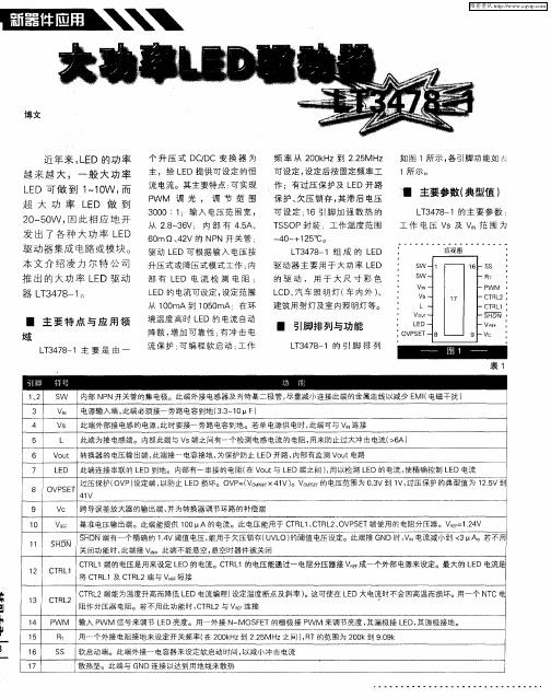

The● denotes the specifi cations which apply over the full operating temperature range, otherwise specifi cations are at T A = 25°C. SW = open, V IN = V S = L = V OUT = S H D N = 2.7V, LED = open, SS = open, PWM = CTRL1, CTRL2 = 1.25V, V REF = open, V C = open, R T = 31.6k.ELECTRICAL CHARACTERISTICSPARAMETER CONDITIONS MIN TYP MAX UNITS Frequency: f OSC 2.25MHz R T = 9.09k2 2.25 2.6MHz Line Regulation f OSC R T = 31.6k, 2.7V < V IN < 36V0.050.2%/V Nominal R T Pin Voltage0.64VMaximum Duty Cycle R T = 31.6kR T = 200kR T = 9.09k ●80889773%%%LED Current to V C Current Gain(Note 6)770µA/A LED Current to V C Voltage Gain(Note 6)400V/A V C to Switch Current Gain13A/V V C Source Current (Out of Pin)CTRL1 = 0.4V, V C = 1V40µA V C Sink Current CTRL1 = 0V, V C = 1V40µA V C Switching Threshold0.65V V C High Level (V OH)CTRL1 = 0.4V 1.5V V C Low Level (V OL)CTRL1 = 0V0.2V Inductor Current Limit 2.7V < V S < 36V● 4.56 6.8A Switch Current Limit● 4.5 6.37.5A Switch V CE SAT I SW = 4.5A270mV Switch Leakage Current SW = 42V, V C = 0V1µAV OUT Overvoltage Protection (OVP) (Rising)OVPSET = 1VOVPSET = 0.3V4112.3VVFull Scale LED Current (LT3478-1)CTRL1 = V REF, Current Out of LED Pin101010501090mA 700mA LED Current (LT3478-1)CTRL1 = 700mV, Current Out of LED Pin●655700730mA 350mA LED Current (LT3478-1)CTRL1 = 350mV, Current Out of LED Pin325350375mA 100mA LED Current (LT3478-1)CTRL1 = 100mV, Current Out of LED Pin70100130mA Full Scale LED Current V SENSE (LT3478)CTRL1 = V REF, V SENSE = V VOUT – V LED101105109mV CTRL1 = 700mV, V SENSE (LT3478)CTRL1 = 700mV, V SENSE = V VOUT – V LED●6770.574mV CTRL1 = 350mV, V SENSE (LT3478)CTRL1 = 350mV, V SENSE = V VOUT – V LED3335.538mV CTRL1 = 100mV, V SENSE (LT3478)CTRL1 = 100mV, V SENSE = V VOUT – V LED71013mV CTRL1, 2 Input Currents CTRL1 = 100mV, CTRL2 = 1.25V orCTRL2 = 100mV, CTRL1 = 1.25V (Current Out of Pin)40nA OVPSET Input Current OVPSET = 1V, V OUT = 41V (Current Out of Pin)200nA PWM Switching Threshold0.81 1.2V V C Pin Current in PWM Mode V C = 1V, PWM = 0150nA OUT Pin Current in PWM Mode PWM = 01100nA SS Low Level (V OL)I(SS) = 20µA0.15V SS Reset Threshold V C = 0V0.25V SS High Level (V OH)V C = 0V 1.5V Soft-Start (SS) Pin Charge Current SS = 1V, Current Out of Pin, V C = 0V12µA Soft-Start (SS) Pin Discharge Current SS = 0.5V, V C = 0V350µA34781f34781fPI FU CTIO SU U USW (Pins 1, 2): Switch Pin. Collector of the internal NPN power switch. Both pins are fused together inside the IC. Connect the inductor and diode here and minimize the metal trace area connected to this pin to minimize EMI.V IN (Pin 3): Input Supply. Must be locally bypassed with a capacitor to ground.V S (Pin 4): Inductor Supply. Must be locally bypassed with a capacitor to ground. Can be shorted to V IN if only one supply is available (see L (Pin 5) function).L (Pin 5): Inductor Pin. An internal resistor between V S and L pins monitors inductor current to protect against inrush current. Exceeding 6A immediately turns off the internal NPN power switch and discharges the soft-start pin. Input current monitoring can be disabled by connect-ing the inductor power supply directly to the L pin and leaving the V S pin open (requires local bypass capacitor to GND on L pin; not V S pin).V OUT (Pin 6): Output voltage of the converter. Connect a capacitor from this pin to ground. Internal circuitry moni-tors V OUT for protection against open LED faults.LED (Pin 7): Connect the LED string from this pin to ground. An internal (LT3478-1)/external (LT3478) resistor between the V OUT and LED pins senses LED current for accurate control.OVPSET (Pin 8): Programs V OUT overvoltage protection level (OVP) to protect against open LED faults. OVP = (OVPSET • 41)V. OVPSET range is 0.3V to 1V for an OVP range of typically 12.3V to 41V.V C (Pin 9): Output of the transconductance error amplifier and compensation pin for the converter regulation loop.V REF (Pin 10): Bandgap Voltage Reference. This pin can supply up to 100µA. Can be used to program CTRL1, CTRL2, OVPSET pin voltages using resistor dividers to ground.SH D N (Pin 11): The S H D N pin has an accurate 1.4V threshold and can be used to program an undervoltage lockout (UVLO) threshold for system input supply using a resistor divider from supply to ground. A 10µA pin currenthysteresis allows programming of undervoltage lockout (UVLO) hysteresis. S H D N above 1.4V turns the part on and removes a 10µA sink current from the pin. S H D N = 0Vreduces V IN current < 3µA. SH D N can be directly connected to V IN . If left open circuit the part will be turned off.CTRL1 (Pin 12): CTRL1 pin voltage is used to program maximum LED current (CTRL2 = V REF ). CTRL1 voltage can be set by a resistor divider from V REF or an external voltage source. Maximum LED current is given by:(LT3478-1) Max LED Current = Min(CTRL1, 1.05) Amps ()(,.)•.LT Max LED Current Min CTRL R SE 347810501=N SEAmps(linear for 0.1V < CTRL1< 0.95V ; CTRL2 = V REF ) For maxi-mum LED current, short CTRL1 and CTRL2 pins to V REF .CTRL2 (Pin 13): The CTRL2 pin is available for program-ming a decrease in LED current versus temperature (setting temperature breakpoint and slope). This feature allows the output LED(s) to be programmed for maximum allowable current without damage at higher temperatures. This maximizes LED usage and increases reliability. A CTRL2 voltage with negative temperature coeffi cient is created using an external resistor divider from V REF with temperature dependant resistance. If not used, CTRL2 should be tied to V REF .PWM (Pin 14): Input pin for PWM dimming control. Above 1V allows converter switching and below 1V disables switching with V C pin level maintained. With an external MOSFET placed in series with the ground side of the LED string, a PWM signal driving the PWM pin and MOSFET gate provides accurate dimming control. The PWM signal can be driven from 0V to 15V. If unused, the pin should be connected to V REF .R T (Pin 15): A resistor to ground programs switching frequency between 200kHz and 2.25MHz.SS (Pin 16): Soft-Start Pin. Placing a capacitor here pro-grams soft-start timing to limit inductor inrush current during start-up due to the converter. When inductor currentOPERATIOUThe LT3478/LT3478-1 are high powered LED drivers with a 42V, 4.5A internal switch and the ability to drive LEDs with up to 1050mA for LT3478-1 and up to 105mV/R SENSE for LT3478.The LT3478/LT3478-1 work similarly to a conventional current mode boost converter but use LED current (instead of output voltage) as feedback for the control loop. The Block Diagram in Figure 1 shows the major functions of the LT3478/LT3478-1.For the part to turn on, the V IN pin must exceed 2.8V and the S H D N pin must exceed 1.4V. The S H D N pin threshold allows programming of an undervoltage lockout (UVLO) threshold for the system input supply using a simple resistor divider. A 10µA current fl ows into the S H D N pin before part turn on and is removed after part turn on. This current hysteresis allows programming of hysteresis for the UVLO threshold. See “Shutdown Pin and Programming Undervoltage Lockout” in the Applications Information Section. For micropower shutdown the S H D N pin at 0V reduces V IN supply current to approximately 3µA. Each LED driver is a current mode step-up switch-ing regulator. A regulation point is achieved when the boosted output voltage V OUT across the output LED(s) is high enough to create current in the LED(s) equal to the programmed LED current. A sense resistor connected in series with the LED(s) provides feedback of LED current to the converter loop.The basic loop uses a pulse from an internal oscillator to set the RS fl ip-fl op and turn on the internal power NPN switch Q1 connected between the switch pin, SW, and ground. Current increases in the external inductor until switch current limit is exceeded or until the oscillator reaches its maximum duty cycle. The switch is then turned off, causing inductor current to lift the SW pin and turn on an external Schottky diode connected to the output. Inductor current fl ows via the Schottky diode charging the output capacitor. The switch is turned back on at the next reset cycle of the internal oscillator. During normal operation the V C voltage controls the peak switch current limit and hence the inductor current available to the output LED(s). As with all current mode converters, slope compensation is added to the control path to ensure stability.The CTRL1 pin is used to program maximum LED current via Q2. The CTRL2 pin can be used to program a decrease in LED current versus temperature for maximum reliability and utilization of the LED(s). A CTRL2 voltage with negative temperature coeffi cient can be created using an external resistor divider from V REF with temperature dependant resistance. Unused CTRL2 is tied to V REF.F or True Color PWM dimming, the LT3478/LT3478-1 provide up to a 3000:1 wide PWM dimming range by al-lowing the duty cycle of the PWM pin (connected to the IC and an external N-channel MOSFET in series with the LED(s)) to be reduced from 100% to as low as 0.033% for a PWM frequency of 100Hz. Dimming by PWM duty cycle, allows for constant LED color to be maintained over the entire dimming range.F or robust operation, the LT3478/LT3478-1 monitor system performance for any of the following faults : V IN or S H D N pin voltages too low and/or inductor current too high and/or boosted output voltage too high. On detection of any of these faults, the LT3478/LT3478-1 stop switching immediately and a soft-start latch is set discharging the SS pin (see Timing Diagram for SS pin in Figure 11). All faults are detected internally and do not require external components. When all faults no longer exist, an internal 12µA supply charges the SS pin with a timing programmed using a single external capacitor. A gradual ramp up of SS pin voltage limits switch current during startup.For optimum component sizing, duty cycle range and ef-fi ciency the LT3478/LT3478-1 allow for a separate inductor supply V S and for switching frequency to be programmed from 200kHz up to 2.25MHz using a resistor from the R T pin to ground. The advantages of these options are covered in the Applications Informations section.34781fAPPLICATIO S I FOR ATIOW UUU Inductor SelectionSeveral inductors that work well with the LT3478/LT3478-1 are listed in Table 1. However, there are many other manu-facturers and inductors that can be used. Consult each manufacturer for more detailed information and their entire range of parts. Ferrite cores should be used to obtain the best effi ciency. Choose an inductor that can handle the necessary peak current without saturating. Also ensure that the inductor has a low DCR (copper-wire resistance) to minimize I 2R power losses. Values between 4.7µH and 22µH will suffi ce for most applications.Inductor manufacturers specify the maximum current rating as the current where inductance falls by a given percentage of its nominal value. An inductor can pass a current greater than its rated value without damaging it. Aggressive designs where board space is precious will exceed the maximum current rating of the inductor to save space. Consult each manufacturer to determine how the maximum inductor current is measured and how much more current the inductor can reliably conduct.Capacitor SelectionLow ESR (equivalent series resistance) ceramic capaci-tors should be used at the output to minimize the output ripple voltage. Use only X5R or X7R dielectrics, as these materials retain their capacitance over wider voltage and temperature ranges than other dielectrics. A 4.7µF to 10µF output capacitor is suffi cient for most high output current designs. Some suggested manufacturers are listed in Table 2.Diode SelectionSchottky diodes, with their low forward voltage drop and fast switching speed, are ideal for LT3478/LT3478-1 ap-plications. Table 3 lists several Schottky diodes that work well. The diode’s average current rating must exceed the application’s average output current. The diode’s maximum reverse voltage must exceed the application’s output volt-age. A 4.5A diode is suffi cient for most designs. For PWM dimming applications, be aware of the reverse leakage current of the diode. Lower leakage current will drain the output capacitor less, allowing for higher dimming range. The companies below offer Schottky diodes with high voltage and current ratings.Table 1. Suggested InductorsMANUFACTURER PART NUMBERIDC (A)INDUCTANCE (µH)MAX DCR (m Ω)L × W × H (mm)MANUFACTURERCDRH104R-100NC CDRH103RNP-4R7NC-B CDRH124R-100MC CDRH104R-5R2NC 3.844.55.5104.7105.23530282210.5 × 10.3 × 4.010.5 × 10.3 × 3.112.3 × 12.3 × 4.510.5 × 10.3 × 4.0Sumida FDV0630-4R7M4.2 4.7497.0 × 7.7 × 3.0Toko UP4B-2207.6223422 × 15 × 7.9CooperTable 2. Ceramic Capacitor ManufacturersMANUFACTURER PHONE NUMBER WEBTaiyo Yuden (408) AVX (803) Murata(714) 852-2001Table 3. Suggested DiodesMANUFACTURER PART NUMBERMAX CURRENT (A)MAX REVERSE VOLTAGEWEB UPS340340Microsemi B520C B530C B340A B540C PDS560553553030404060Diodes, APPLICATIO S I FOR ATIOW UUU allowed level at higher temperatures, the CTRL2 voltagecurve may require a greater downward slope between 25°C and 50°C to compensate for that loss of slope at higher temperatures.Example: Calculate the resistor values required for generat-ing CTRL1 and CTRL2 from V REF based on the following requirements:(a) I LED = 700mA at 25°C(b) I LED derating curve breakpoint occurs at 25°C (c) I LED derating curve has a slope of –200mA/25°C be-tween 25°C and 50°C ambient temperature Step1: Choose CTRL1 = 700mV for I LED = 700mA CTRL1 = V REF /(1 + R2/R1) R2 = R1 • [(V REF /CTRL1) – 1]For V REF = 1.24V and choosing R1 = 22.1k, R2 = 22.1k [(1.24/0.7) – 1] R2 = 17k (choose 16.9k) CTRL1 = 1.24/(1 + (16.9/22.1)) CTRL1 = 703mV (I LED = 703mA)Step 2: Choose resistor network option A (Figure 7) and CTRL2 = CTRL1 for 25°C breakpoint start with R4 = R2 = 16.9k, R NTC = 22k (closest value available)CTRL2 = 701mV (I LED = Min(CTRL1, CTRL2) • 1A = 701mA)Step 3: Calculate CTRL2 slope between 25°C and 50°C CTRL2 (T) = 1.24/(1 + R4/R NTC (T)) at T = T O = 25°C, CTRL2 = 701mVat T = 50°C, R NTC (T) = R NTC (T O ).e x , x = B [(1/(T + 273) – 1/298)](B = B-constant; linear over the 25°C to 50°C temperature range)or R NTC B-constant = 3950 and T = 50°C x = 3950 [(1/323) – 1/298] = –1.026R NTC (50°C) = R NTC (25°C).e –1.026 R NTC (50°C) = 22k • 0.358R NTC (50°C) = 7.9kCTRL2(50°C) = 1.24/(1 + 16.9/7.9) = 395mV CTRL2 slope (25°C to 50°C) = [CTRL2(50°C) – CTRL2(25°C)]/25°C = (395 – 701)/25 = –306mV/25°CI LED slope = –306mA/25°CThe required I LED slope is –200mA/25°C. To reduce the slope of CTRL2 versus temperature it is easier to keep the exact same NTC resistor value and B-constant (there are limited choices) and simply adjust R4 and the type of resistor network used for the CTRL2 pin. By changing the resistor network to option C it is possible to place a temperature independent resistor in series with R NTC to reduce the effects of R NTC on the CTRL2 pin voltage over temperature.Step 4: Calculate the resistor value required for R Y in resistor network option (c) (Figure 7) to provide an I LED slope of –200mA/25°C between 25°C and 50°C ambient temperature.CTRL2 (25°C) = 0.7V = 1.24/(1 + (R4/(R NTC (25°C)+ R Y )) R4 = 0.77 (R NTC (25°C) + R Y ) (a) for –200mA/25°C slope ≥ CTRL2(50°C) = 0.7 – 0.2 = 0.5CTRL2(50°C) = 0.5V = 1.24/(1 + (R4/(R NTC + R Y )) R4 = 1.48 (R NTC (50°C) + R Y ) (b) Equating (a) = (b) and knowing R NTC (25°C) = 22k and R NTC (50°C) = 7.9k gives, 0.77 (22k + R Y ) = 1.48 (7.9k + R Y ) 17k + 0.77 R Y = 11.7 k + 1.48 R Y R Y = (17k – 11.7k)/(1.48 – 0.77) R Y = 7.5k34781fAPPLICATIO S I FOR ATIOW UUU LT3478/LT3478-1 immediately stop switching, a soft-start latch is set and the SS pin is discharged. The SS latch can only be reset when V OUT falls below OVP and the SS pin has been discharged below 0.25V (F igure 11). If the LED(s) simply go open circuit and are reconnected, however, the OVP used to protect the switch might be too high for the reconnected LED(s). The LT3478/LT3478-1 therefore allow OVP to be programmable to protect both the LED driver switch and the LED(s). (The minimum allowable OVP for normal operation for a given LED string depends on the number of LEDs and their maximum forward voltage rat-ings.) OVP is programmed using the OVPSET pin (front page), given by, OVP = (OVPSET • 41)Vwhere the programmable range for the OVPSET pin is 0.3V to 1V resulting in an OVP range of 12.3V to 41V.The OVPSET pin can be programmed with a single resistor by tapping off of the resistor divider from V REF used to program CTRL1. If both CTRL1 and CTRL2 are connected directly to V REF (maximum LED current setting) then OVP-SET requires a simple 2 resistor divider from V REF .Thermal CalculationsTo maximize output power capability in an application without exceeding the LT3478/LT3478-1 125°C maximum operational junction temperature, it is useful to be able to calculate power dissipation within the IC. The power dissipation within the IC comes from four main sources: switch DC loss, switch AC loss, Inductor and LED cur-rent sensing and input quiescent current. These formulas assume a boost converter architecture, continuous mode operation and no PWM dimming.(1) Switch DC loss = P SW(DC)= (R SW • I L(AVE)2 • D)R SW = switch resistance = 0.07Ω (at T J = 125°C)I L(AVE) = P OUT /(η • V S )P OUT = V OUT • I LED η = converter effi ciency = P OUT /(P OUT + P LOSS )V S = inductor supply inputD = switch duty cycle = (V OUT + V F – V S )/(V OUT + V F – V SAT ) V F = forward voltage drop of external Schottky diode V SAT = I L(AVE) • R SW(2) Switch AC loss = P SW(AC)= t EFF (1/2)I L(AVE)(V OUT + V F )(F OSC )t EFF = effective switch current and switch V CE voltageoverlap time during turn on and turn off = 2 • (t ISW + t VSW )t ISW = I SWITCH rise/fall time = I L(AVE) • 2ns t VSW = SW fall/rise time = (V OUT + V F ) • 0.7ns f OSC = switching frequency (3) Current sensing loss = P SENSE = P SENSE(IL) + P SENSE(ILED) P SENSE(IL) = I L(AVE)2 • 9.5m Ω P SENSE(ILED) = I LED 2 • 0.1Ω(4) Input quiescent loss = P Q = V IN • I Q where I Q = (6.2mA + (100mA • D))Example (Using LT3478-1):For V IN = V S = 8V, I LED = 700mA, V OUT = 24.5V (7 LEDs), V F = 0.5V and f OSC = 0.2Mhz, η = 0.89 (initial assumption) I L(AVE) = (24.5 • 0.7)/(0.89 • 8) = 2.41A D = (24.5 + 0.5 – 8)/(24.5 + 0.5 – 0.17) = 0.684 T EFF = 2 • ((2.41 • 2)ns + (24.5 + 0.5) • 0.7)ns = 45ns Total Power Dissipation:P IC = P SW(DC) + P SW(AC) + P SENSE + P Q P SW(DC) = 0.07 • (2.41)2 • 0.684 = 0.278WP SW(AC) = 45ns • 0.5 • 2.41 • 25 • 0.2MHz = 0.271W P SENSE = ((2.41)2 • 0.0095) + ((0.7)2 • 0.1) = 0.104W P Q = 8 • (6.2mA + (100mA • 0.684)) = 0.597W P IC = 0.278 + 0.271 + 0.104 + 0.597 = 1.25WLocal heating from the nearby inductor and Schottky diode will also add to the fi nal junction temperature of the IC. Based on empirical measurements, the effect of diode and inductor heating on the LT3478-1 junction temperature can be approximated as:ΔT J (LT3478-1) = 5°C/W • (P DIODE + P INDUCTOR ) P DIODE = (1 – D) • V F • I L(AVE) 1 – D = 0.316 V F = 0.5VI L(AVE) = 2.41P DIODE = 0.316 • 0.5 • 2.41 = 0.381W P INDUCTOR = I L(AVE)2 • DCRDCR = inductor DC resistance (assume 0.05Ω) P INDUCTOR = (2.41)2 • 0.05 = 0.29WThe LT3478/LT3478-1 use a thermally enhanced FE pack-age. With proper soldering to the Exposed Pad on the underside of the package combined with a full copper plane underneath the device, thermal resistance (θJA ) will be about 35°C/W. For an ambient temperature of T A = 70°C, the junction temperature of the LT3478-1 for the example application described above, can be calculated as: T J (LT3478-1)= T A + θJA (P TOT ) + 5(P DIODE + P INDUCTOR ) = 70 + 35(1.25) + 5(0.671) = 70 + 44 + 4 = 118°CIn the above example, effi ciency was initially assumed to be η = 0.89. A lower effi ciency (η) for the converter will increase I L(AVE) and hence increase the calculated value for T J . η can be calculated as: η = P OUT /(P OUT + P LOSS ) P OUT = V OUT • I LED = 17.15WP LOSS (estimated) = P IC + P DIODE + P INDUCTOR = 1.92W η = 17.15/(17.15 + 1.92) = 0.9If an application is built, the inductor current can be mea-sured and a new value for junction temperature estimated. Ideally a thermal measurement should be made to achieve the greatest accuracy for T J .Note: The junction temperature of the IC can be reduced if a lower V IN supply is available – separate from the inductor supply V S . In the above example, driving V IN from an available 3V source (instead of V S = 8V) reduces input quiescent losses in item(4) from 0.597W to 0.224W, resulting in a reduction of T J from 118°C to 105°yout ConsiderationsAs with all switching regulators, careful attention must be given to PCB layout and component placement to achieve optimal thermal,electrical and noise performance (Figure 12). The exposed pad of the LT3478/LT3478-1 (Pin 17) is the only GND connection for the IC. The exposed pad should be soldered to a continuous copper ground plane underneath the device to reduce die temperature and maximize the power capability of the IC. The ground path for the R T resistor and V C capacitor should be taken from nearby the analog ground connection to the exposed pad (near Pin 9) separate from the power ground connection to the exposed pad (near Pin 16). The bypass capacitor for V IN should be placed as close as possible to the V IN pin and the analog ground connection. SW pin voltage rise and fall times are designed to be as short as possible for maximum effi ciency. To reduce the effects of both radiated and conducted noise, the area of the SW trace should be kept as small as possible. Use a ground plane under the switching regulator to minimize interplane coupling. The schottky diode and output capacitor should be placed as close as possible to the SW node to minimize this high frequency switching path. To minimize LED current sensing errors for the LT3478, the terminals of the external sense resistor R SENSE should be tracked to the V OUT and LED pins separate from any high current paths.APPLICATIO S I FOR ATIOW UUUf PWM = 100Hz3478 TA02b2µs/DIVInformation furnished by Linear Technology Corporation is believed to be accurate and reliable. However, no responsibility is assumed for its use. Linear Technology Corporation makes no representa-tion that the interconnection of its circuits as described herein will not infringe on existing patent rights.Linear Technology Corporation1630 McCarthy Blvd., Milpitas, CA 95035-7417(408) 432-1900 ● FAX: (408) 434-0507 ● © LINEAR TECHNOLOGY CORPORA TION 2007LT 0107 • PRINTED IN USA。