boost 升压芯片 ap3015
- 格式:pdf
- 大小:202.71 KB
- 文档页数:11
30V转15V,12V,9V,8V,6V,5V,3.3V,3V芯片,DC-DC降压和LDO
30V转15V ,30V转12V,30V转9V,30V转8V , 30V转6V ,30V转5V,30V转3.3V,30V转3V,30V转1.8V
30V转15V降压芯片,30V转12V降压芯片,30V转9V降压芯片,30V转8V降压芯片, 30V转6V降压芯片,30V转5V降压芯片,30V转3.3V降压芯片,30V转3V降压芯片,30V转1.8V
30V电压的设备其实很多的,工程师常用的直流电源也是以30V为居多。
注意,不管是DC-DC还是LDO芯片,开关导通输入时,直接30V输入时,在通电和接上电时,会产生输入尖峰高几倍左右电压,这不关有没有芯片问题,是电源固定的特性。
所以输入需要用电解电容或者TVS管或者输入正极串联电阻一般这三种方案来吸收尖
PW6206,输出电压3V,3.3V,5V,输入电压最高40V,功耗也低4uA;
PW8600,输出电压3V,3.3V,5V,输入电压最高80V,功耗也低2uA;
在30V输入中,比较合适的DC-DC可以选择:0.8A的PW2558,2A的PW2902和3A的
PW2153以及以上都最合适的。
PW2558是一颗DC-DC降压转换器芯片,输入电压范围4.5V-55V,最大负载电流0.8A,可调输出电压,频率1.2MHZ高频率,可采用贴片电感,节省空间,采用SOP8封装形式。
PW2902是一颗DC-DC降压转换器芯片,输入电压范围8V-90V,可负载2A,可调输出电压,频率140kHZ。
适用于输出12V2A或者5V2A,可调输出电压5V-30V之间。
PW2153适用于输出12V10A或者5V3A,可调输出电压5V-30V之间。
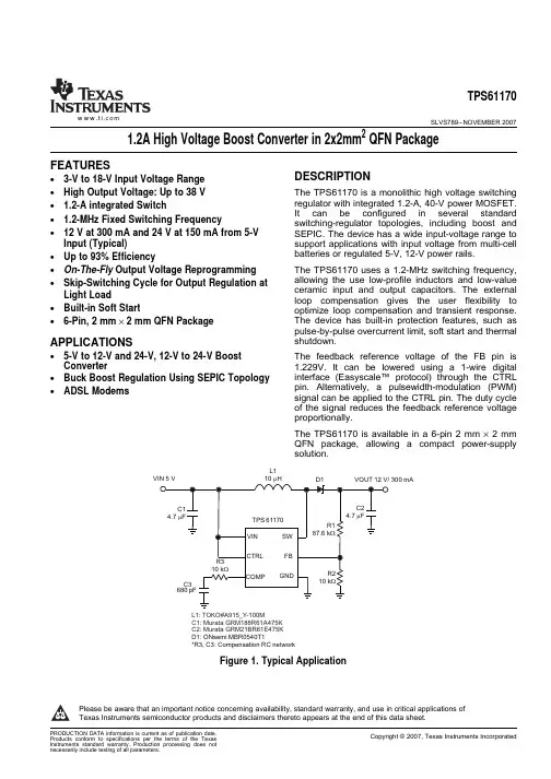
FEATURESDESCRIPTIONAPPLICATIONSL1L1:TOKO#A915_Y-100MC1: Murata GRM188R61A475K C2: Murata GRM21BR61E475K D1:ONsemi MBR0540T1*R3, C3: Compensation RC networkTPS61170SLVS789–NOVEMBER 20071.2A High Voltage Boost Converter in 2x2mm 2QFN Package•3-V to 18-V Input Voltage Range •High Output Voltage:Up to 38V The TPS61170is a monolithic high voltage switching regulator with integrated 1.2-A,40-V power MOSFET.• 1.2-A integrated SwitchIt can be configured in several standard • 1.2-MHz Fixed Switching Frequencyswitching-regulator topologies,including boost and •12V at 300mA and 24V at 150mA from 5-V SEPIC.The device has a wide input-voltage range to Input (Typical)support applications with input voltage from multi-cell batteries or regulated 5-V,12-V power rails.•Up to 93%EfficiencyThe TPS61170uses a 1.2-MHz switching frequency,•On-The-Fly Output Voltage Reprogramming allowing the use low-profile inductors and low-value •Skip-Switching Cycle for Output Regulation at ceramic input and output capacitors.The external Light Loadloop compensation gives the user flexibility to •Built-in Soft Startoptimize loop compensation and transient response.The device has built-in protection features,such as •6-Pin,2mm ×2mm QFN Packagepulse-by-pulse overcurrent limit,soft start and thermal shutdown.•5-V to 12-V and 24-V,12-V to 24-V Boost The feedback reference voltage of the FB pin is Converter1.229V.It can be lowered using a 1-wire digital interface (Easyscale™protocol)through the CTRL •Buck Boost Regulation Using SEPIC Topology pin.Alternatively,a pulsewidth-modulation (PWM)•ADSL Modemssignal can be applied to the CTRL pin.The duty cycle of the signal reduces the feedback reference voltage proportionally.The TPS61170is available in a 6-pin 2mm ×2mm QFN package,allowing a compact power-supply solution.Figure 1.Typical ApplicationPlease be aware that an important notice concerning availability,standard warranty,and use in critical applications of Texas Instruments semiconductor products and disclaimers thereto appears at the end of this data sheet.PRODUCTION DATA information is current as of publication date.Copyright ©2007,Texas Instruments IncorporatedProducts conform to specifications per the terms of the Texas Instruments standard warranty.Production processing does not necessarily include testing of all parameters.ABSOLUTE MAXIMUM RATINGSDISSIPATION RATINGSRECOMMENDED OPERATING CONDITIONSTPS61170SLVS789–NOVEMBER 2007These devices have limited built-in ESD protection.The leads should be shorted together or the device placed in conductive foam during storage or handling to prevent electrostatic damage to the MOS gates.ORDERING INFORMATION (1)T APACKAGE (2)PACKAGE MARKING–40°C to 85°CTPS61170DRVBZS(1)For the most current package and ordering information,see the TI Web site at .(2)The DRV package is available in tape and reel.Add R suffix (TPS61170DRVR)to order quantities of 3000parts per reel or add T suffix (TPS61170DRVT)to order 250parts per reel.over operating free-air temperature range (unless otherwise noted)(1)VALUE UNIT Supply Voltages on VIN(2)–0.3to 20V Voltages on CTRL (2)–0.3to 20V V IVoltage on FB and COMP(2)–0.3to 3V Voltage on SW (2)–0.3to 40V P D Continuous Power DissipationSee Dissipation Rating TableT J Operating Junction Temperature Range –40to 150°C T STG Storage Temperature Range–65to 150°C(1)Stresses beyond those listed under absolute maximum ratings may cause permanent damage to the device.These are stress ratings only,and functional operation of the device at these or any other conditions beyond those indicated under recommended operating conditions is not implied.Exposure to absolute-maximum-rated conditions for extended periods may affect device reliability.(2)All voltage values are with respect to network ground terminal.DERATING FACTOR BOARD PACKAGER θJC R θJA T A <25°C T A =70°C T A =85°C ABOVE T A =25°CLow-K (1)DRV 20°C/W 140°C/W 7.1mW/°C 715mW 395mW 285mW High-K (2)DRV20°C/W65°C/W15.4mW/°C1540mW845mW615mW(1)The JEDEC low-K (1s)board used to derive this data was a 3in ×3in,two-layer board with 2-ounce copper traces on top of the board.(2)The JEDEC high-K (2s2p)board used to derive this data was a 3in ×3in,multilayer board with 1-ounce internal power and ground planes and 2-ounce copper traces on top and bottom of the board.MINTYP MAX UNIT V I Input voltage range,VIN 318V V O Output voltage range VIN 38V L Inductor(1)1022µH C I Input capacitor 1µF C O Output capacitor110µF T A Operating ambient temperature –4085°C T J Operating junction temperature–40125°C(1)These values are recommended values that have been successfully tested in several applications.Other values may be acceptable in other applications but should be fully tested by the user.2Submit Documentation FeedbackCopyright ©2007,Texas Instruments IncorporatedProduct Folder Link(s):TPS61170ELECTRICAL CHARACTERISTICSTPS61170 SLVS789–NOVEMBER2007VIN=3.6V,CTRL=VIN,T A=–40°C to85°C,typical values are at T A=25°C(unless otherwise noted)PARAMETER TEST CONDITIONS MIN TYP MAX UNITSUPPLY CURRENTV I Input voltage range,VIN 3.018VI Q Operating quiescent current into VIN Device PWM switching no load 2.3mAI SD Shutdown current CRTL=GND,VIN=4.2V1µAUVLO Under-voltage lockout threshold VIN falling 2.2 2.5VV hys Under-voltage lockout hysterisis70mVENABLE AND REFERENCE CONTROLV(CTRLh)CTRL logic high voltage VIN=3V to18V 1.2VV(CTRL)CTRL logic low voltage VIN=3V to18V0.4VR(CTRL)CTRL pull down resistor4008001600kΩt off CTRL pulse width to shutdown CTRL high to low 2.5mst es_det Easy Scale detection time(1)CTRL pin low260µst es_delay Easy Scale detection delay100µst es_win Easy Scale detection window time1msVOLTAGE AND CURRENT CONTROLV REF Voltage feedback regulation voltage 1.204 1.229 1.254VVoltage feedback regulation voltage underV(REF_PWM)V FB=492mV477492507mV reprogramI FB Voltage feedback input bias current V FB=1.229V200nAf S Oscillator frequency 1.0 1.2 1.5MHzD max Maximum duty cycle V FB=100mV90%93%t min_on Minimum on pulse width40nsI sink Comp pin sink current100µAI source Comp pin source current100µAG ea Error amplifier transconductance240320400umhoR ea Error amplifier output resistance5pF connected to COMP6MΩf ea Error amplifier crossover frequency5pF connected to COMP500kHzPOWER SWITCHVIN=3.6V0.30.6R DS(on)N-channel MOSFET on-resistanceΩVIN=3.0V0.7I LN_NFET N-channel leakage current V SW=35V,T A=25°C1µAOC and SSI LIM N-Channel MOSFET current limit D=D max0.96 1.2 1.44AI LIM_Start Start up current limit D=D max0.7At Half_LIM Time step for half current limit5mst REF Vref filter time constant180µst step V REF ramp up time213µs (1)EasyScale communication is allowed immediately after the CTRL pin has been low for more than t es_det.To select EasyScale™mode,the CTRL pin must be low for more than t es_det the end of t es_win.Copyright©2007,Texas Instruments Incorporated Submit Documentation Feedback3Product Folder Link(s):TPS61170PIN ASSIGNMENTSVIN CTRLSWFBCOMPGND TOPVIEW6-PIN 2mm x 2mm x 0.8mm QFNTPS61170SLVS789–NOVEMBER 2007ELECTRICAL CHARACTERISTICS (continued)VIN =3.6V,CTRL =VIN,T A =–40°C to 85°C,typical values are at T A =25°C (unless otherwise noted)PARAMETERTEST CONDITIONS MIN TYP MAX UNIT EasyScale TIMING t start Start time of program stream 2µst EOS End time of program stream 2360µs t H_LB High time low bit Logic 02180µs t L_LB Low time low bit Logic 02×t H_LB 360µs t H_HB High time high bit Logic 12×t L_HB360µs t L_HB Low time high bitLogic 12180µs V ACKNL Acknowledge output voltage low Open drain,R pullup =15k Ωto Vin 0.4V t valACKN Acknowledge valid timeSee (2)2µs t ACKN Duration of acknowledge condition See(2)512µs THERMAL SHUTDOWNT shutdown Thermal shutdown threshold160°C T hysteresis Thermal shutdown threshold hysteresis15°C(2)Acknowledge condition active 0,this condition will only be applied if the RFA bit is set.Open drain output,line needs to be pulled high by the host with resistor load.TERMINAL FUNCTIONSTERMINAL I/O DESCRIPTIONNAME NO.VIN 6I The input supply pin for the IC.Connect VIN to a supply voltage between 3V and 18V.SW 4I This is the switching node of the IC.Connect SW to the switched side of the inductor.GND 3O GroundFB 1I Feedback pin for current.Connect to the center tap of a resistor divider to program the output voltage.Output of the transconductance error amplifier.Connect an external RC network to this pin to compensate COMP 2O the regulator.Control pin of the boost regulator.CTRL is a multi-functional pin which can be used for enable the device CTRL 5Iand control the feedback voltage with a PWM signal and digital communications.The thermal pad should be soldered to the analog ground plane to avoid thermal issue.If possible,use Thermal Padthermal via to connect to ground plane for ideal power dissipation.4Submit Documentation FeedbackCopyright ©2007,Texas Instruments IncorporatedProduct Folder Link(s):TPS61170FUNCTIONAL BLOCK DIAGRAMTYPICAL CHARACTERISTICS TABLE OF GRAPHSTPS61170 SLVS789–NOVEMBER2007Circuit of Figure1,L=TOKO A915_Y-100M,D1=ONsemi MBR0540T1,unless otherwise noted.FIGURE Efficiency VIN=5V;VOUT=12V,18V,24V,30V;Figure2 Efficiency VIN=5V,8.5V,12V;VOUT=24V;Figure3 Output voltage accuracy I LOAD=100mA Figure4 Switch current limit T A=25°C Figure5 Switch current limit Figure6Error amplifier transconductance Figure7 Easyscale step Figure8PWM switching operation VIN=5V;VOUT=12V;I LOAD=250mA;Figure9Load transient response VIN=5V;VOUT=12V;I LOAD=50mA to150mA;Figure10Start-up VIN=5V;VOUT=12V;I LOAD=250mA;Figure11Skip-cycle switching VIN=9V;VOUT=12V,I LOAD=100µA;Figure12Copyright©2007,Texas Instruments Incorporated Submit Documentation Feedback5Product Folder Link(s):TPS61170405060708090100E f f i c i e n c y - %Output Current - mA507080050100150200250300E f f i c i e n c y - %Output Current - mA11.90V - Input Voltage - VI V - O u t p u t V o l t a g e - VO 80090010001100120013001400150016002030405060708090Duty Cycle - %S w i t c h C u r r e n t L i m i t -A8009001000110012001300140015001600-40-20020406080100120140Temperature -C°S w i t c h C u r r e n t L i m i t - m A0100200300400500-40-20020406080100120140Temperature -C°E r r o r A m p l i f i e r T r a n s c o n d u c t a n c e - m h o sTPS61170SLVS789–NOVEMBER 2007EFFICIENCYEFFICIENCYvsvsOUTPUT CURRENTOUTPUT CURRENTFigure 2.Figure 3.OUTPUT VOLTAGESWITCH CURRENT LIMITvsvsINPUT VOLTAGEDUTY CYCLEFigure 4.Figure 5.SWITCH CURRENT LIMITERROR AMPLIFIER TRANSCONDUCTANCEvsvsTEMPERATURETEMPERATUREFigure 6.Figure 7.6Submit Documentation FeedbackCopyright ©2007,Texas Instruments IncorporatedProduct Folder Link(s):TPS611700.20.40.60.811.21.402468101214161820222426283032Easy Scale StepF B Vo l t a g e - Vt - 1 ms/divTPS61170SLVS789–NOVEMBER 2007FB VOLTAGEvsEASY SCALE STEPPWM SWITCHING OPERATIONFigure 8.Figure 9.LOAD TRANSIENT RESPONSESTART-UPFigure 10.Figure 11.SKIP-CYCLE SWITCHINGFigure 12.Copyright ©2007,Texas Instruments Incorporated Submit Documentation Feedback7Product Folder Link(s):TPS61170DETAILED DESCRIPTIONOPERATIONSOFT START-UPOVERCURRENT PROTECTIONUNDERVOLTAGE LOCKOUT (UVLO)THERMAL SHUTDOWNENABLE AND SHUTDOWNTPS61170SLVS789–NOVEMBER 2007The TPS61170integrates a 40-V low side FET for up to 38-V output voltages.The device regulates the output with current mode PWM (pulse width modulation)control.The switching frequency of PWM is fixed at 1.2MHz.The PWM control circuitry turns on the switch at the beginning of each switching cycle.The input voltage is applied across the inductor and stores the energy as inductor current ramps up.During this portion of the switching cycle,the load current is provided by the output capacitor.When the inductor current rises to the threshold set by the error amplifier output,the power switch turns off and the external Schottky diode is forward biased.The inductor transfers stored energy to replenish the output capacitor and supply the load current.This operation repeats in every switching cycle.As shown in the block diagram,the duty cycle of the converter is determined by the PWM control comparator which compares the error amplifier output and the current signal.A ramp signal from oscillator is added to the current ramp.This slope compensation is to avoid sub-harmonic oscillation that is intrinsic to the current mode control at duty cycle higher than 50%.The feedback loop regulates the FB pin to a reference voltage through an error amplifier.The output of the error amplifier is connected to the COMP pin.An external RC compensation network is connected to the COMP pin to optimize the feedback loop for stability and transient response.Soft-start circuitry is integrated into the IC to avoid a high inrush current during start-up.After the device is enabled by a logic high signal on the CTRL pin,the FB pin reference voltage ramps up in 32steps,each step takes 213µs.This ensures that the output voltage rises slowly to reduce inrush current.Additionally,for the first 5msec after the COMP voltage ramps,the current limit of the PWM switch is set to half of the normal current limit spec.Therefore,during this period the input current is kept below 700mA (typical).See the start-up waveform for a typical example,Figure 11.TPS61170has a cycle-by-cycle overcurrent limit feature that turns off the power switch once the inductor current reaches the overcurrent limit.The PWM circuitry resets itself at the beginning of the next switch cycle.During an over-current event,this results in a decrease of output voltage with respect to load.The current limit threshold as well as input voltage,output voltage,switching frequency and inductor value determine the maximum available output rger inductor values increases the current output capability because of the reduced current ripple.See the APPLICATION INFORMATION section for the output current calculation.An undervoltage lockout prevents mis-operation of the device at input voltages below typical 2.2V.When the input voltage is below the undervoltage threshold,the device remains off and the internal switch FET is turned off.The undervoltage lockout threshold is set below minimum operating voltage of 3V to avoid any transient VIN dip triggering the UVLO and causing the device to reset.For the input voltages between UVLO threshold and 3V,the device maintains its operation,but the specifications are not ensured.An internal thermal shutdown turns off the device when the typical junction temperature of 160°C is exceeded.The IC restarts when the junction temperature drops by 15°C.The TPS61170enters shutdown when the CTRL voltage is less than 0.4V for more than 2.5ms.In shutdown,the input supply current for the device is less than 1µA (max).The CTRL pin has an internal 800k Ωpull down resistor to disable the device when the pin is left unconnected.8Submit Documentation FeedbackCopyright ©2007,Texas Instruments IncorporatedProduct Folder Link(s):TPS61170FEEDBACK REFERENCE PROGRAM MODE SELECTIONCTRLlowhigh FB200mV x duty cycleInsert batteryCTRLlowhigh FBInsert batteryProgrammingcode50mV 50mVEnter ES modeV FB +Duty 1.229V (1)TPS61170SLVS789–NOVEMBER 2007The CTRL pin is used for changing the FB pin reference voltage on-the-fly .There are two methods to program the reference voltage,PWM signal and 1wire interface (EasyScale™).The program mode is selected each time the device is enabled.The default mode is the PWM signal which uses the duty cycle of the CTRL pin signal to modulate the reference voltage.To enter the 1wire interface mode,the following digital pattern on the CTRL pin must be recognized by the IC every time the IC starts from the shutdown mode.1.Pull CTRL pin high to enable the TPS61170and to start the 1wire mode detection window.2.After the EasyScale detection delay (t es_delay ,100µsec)expires,drive CTRL low for more than the EasyScale detection time (t es_detect ,260µsec).3.The CTRL pin has to be low for more than EasyScale detection time before the EasyScale detection window (t es_win ,1msec)expires.EasyScale detection window starts from the first CTRL pin low to high transition.The IC immediately enters the 1wire mode once the above 3conditions are met.The EasyScale communication can start before the detection window expires.Once the mode is programmed,it can not be changed without another start up.This means the IC needs to be shutdown by pulling the CTRL low for 2.5ms and restarts.See the Mode Detection of Feedback Reference Program figure (Figure 13)for a graphical explanation.Figure 13.Mode Detection of Feedback Reference ProgramWhen the CTRL pin is constantly high,the FB voltage is regulated to 1.229V typically.However,the CTRL pinallows a PWM signal to reduce this regulation voltage.The relationship between the duty cycle and FB voltage is given in Equation 1:Where:Duty =duty cycle of the PWM signal 1.229V =internal reference voltageAs shown in Figure 14,the IC chops up the internal 1.229V reference voltage at the duty cycle of the PWM signal.The pulse signal is then filtered by an internal low pass filter.The output of the filter is connected to the error amplifier as the reference voltage for the FB pin regulation.The regulation voltage is independent of the PWM logic voltage level which often has large variations.For optimum performance,use the PWM mode in the range of 5kHz to 100kHz.The requirement of minimum frequency comes from the EasyScale detection delay and detection time specification for the mode selection.The device can mistakenly enter 1wire mode if the PWM signal frequency is less than 5kHz.Since the CTRL pin is logic only pin,adding external RC filter to the pin does not work.Copyright ©2007,Texas Instruments IncorporatedSubmit Documentation Feedback9Product Folder Link(s):TPS61170VBG1.229 V1WIRE PROGRAM MODEEasyScale™TPS61170SLVS789–NOVEMBER2007Figure14.Block Diagram of Programmable FB Voltage Using PWM SignalThe CTRL pin features a simple digital interface to control the feedback reference voltage.The1wire mode can save the processor power and battery life as it does not require a PWM signal all the time,and the processor can enter idle mode if available.The TPS61170adopts the EasyScale™protocol,which can program the FB voltage to any of the32steps with single command.See the Table1for the FB pin voltage steps.The programmed reference voltage is stored in an internal register.The default value is full scale when the device is first enabled(V FB=1.229V).A power reset clears the register value and reset it to default.EasyScale is a simple but very flexible one pin interface to configure the FB voltage.The interface is based on a master-slave structure,where the master is typically a microcontroller or application processor.Figure15and Table1give an overview of the protocol.The protocol consists of a device specific address byte and a data byte. The device specific address byte is fixed to72hex.The data byte consists of five bits for information,two address bits,and the RFA bit.The RFA bit set to high indicates the Request for Acknowledge condition.The Acknowledge condition is only applied if the protocol was received correctly.The advantage of EasyScale compared with other on pin interfaces is that its bit detection is in a large extent independent from the bit transmission rate.It can automatically detect bit rates between1.7kBit/sec and up to160kBit/sec.Table1.Selectable FB VoltageFB voltageD4D3D2D1D0(mV)00.0000000010.0310000120.0490001030.0680001140.0860010050.1040010160.1230011070.1410011180.1600100090.17801001100.19701010110.21501011120.23401100130.27001101140.3070111010Submit Documentation Feedback Copyright©2007,Texas Instruments IncorporatedProduct Folder Link(s):TPS61170DATA INDATA OUTTPS61170SLVS789–NOVEMBER 2007Table 1.Selectable FB Voltage (continued)FB voltage D4D3D2D1D0(mV)150.34401111160.38110000170.41810001180.45510010190.49210011200.52810100210.56510101220.60210110230.63910111240.71311000250.78711001260.86011010270.9341101128 1.0081110029 1.0821110130 1.15511110311.22911111Figure 15.EasyScale™Protocol Overview Table 2.EasyScale™Bit DescriptionBIT TRANSMISSION BYTENAME DESCRIPTIONNUMBERDIRECTION7DA70MSB device address 6DA615DA51Device 4DA41Address INByte 3DA3072hex2DA201DA110DA00LSB device address7(MSB)RFA Request for acknowledge.If high,acknowledge is applied by device 6A10Address bit 15A00Address bit 04D4Data bit 4Data byteIN 3D3Data bit 32D2Data bit 21D1Data bit 10(LSB)D0Data bit 0Copyright ©2007,Texas Instruments Incorporated Submit Documentation Feedback11Product Folder Link(s):TPS61170Easy Scale Timing, without acknowledge RFA = 0DATA INEasy Scale Timing, with acknowledge RFA = 1Acknowledge true , Data Line pulled down by device DATA INDATA Acknowledge false , no pull downTPS61170SLVS789–NOVEMBER 2007Table 2.EasyScale™Bit Description (continued)BIT TRANSMISSION BYTENAMEDESCRIPTIONNUMBERDIRECTIONAcknowledge condition active 0,this condition will only be applied in case RFA bit is set.Open drain output,Line needs to be pulled high by the host with a pullupACKOUTresistor.This feature can only be used if the master has an open drain output stage.In case of a push pull output stage Acknowledge condition may not be requested!Figure 16.EasyScale™—Bit CodingAll bits are transmitted MSB first and LSB last.Figure 16shows the protocol without acknowledge request (Bit RFA =0),Figure 16with acknowledge (Bit RFA =1)request.Prior to both bytes,device address byte and data byte,a start condition must be applied.For this,the CTRL pin must be pulled high for at least t start (2µs)before the bit transmission starts with the falling edge.If the CTRL pin is already at high level,no start condition is needed prior to the device address byte.The transmission of each byte is closed with an End of Stream condition for at least t EOS (2µs).12Submit Documentation FeedbackCopyright ©2007,Texas Instruments IncorporatedProduct Folder Link(s):TPS61170TPS61170 SLVS789–NOVEMBER2007The bit detection is based on a Logic Detection scheme,where the criterion is the relation between t LOW and t HIGH.It can be simplified to:High Bit:t HIGH>t LOW,but with t HIGH at least2x t LOW,see Figure16.Low Bit:t HIGH<t LOW,but with t LOW at least2x t HIGH,see Figure16.The bit detection starts with a falling edge on the CTRL pin and ends with the next falling edge.Depending on the relation between t HIGH and t LOW,the logic0or1is detected.The acknowledge condition is only applied if:•Acknowledge is requested by a set RFA bit.•The transmitted device address matches with the device address of the device.•16bits is received correctly.If the device turns on the internal ACKN-MOSFET and pulls the CTRL pin low for the time t ACKN,which is512µs maximum then the Acknowledge condition is valid after an internal delay time t valACK.This means that the internal ACKN-MOSFET is turned on after t valACK,when the last falling edge of the protocol was detected.The master controller keeps the line low in this period.The master device can detect the acknowledge condition with its input by releasing the CTRL pin after t valACK and read back a logic0.The CTRL pin can be used again after the acknowledge condition ends.Note that the acknowledge condition may only be requested if the master device has an open drain output.For the push-pull output stage,the use a series resistor in the CRTL line to limit the current to500µA is recommended for such cases as:•an accidentally requested acknowledge,or•to protect the internal ACKN-MOSFET.Copyright©2007,Texas Instruments Incorporated Submit Documentation Feedback13Product Folder Link(s):TPS61170APPLICATION INFORMATIONPROGRAM OUTPUT VOLTAGEVOUTR1Vout Vout =1.229V x +1R1=R2x 1R2 1.229V -æöæöç÷ç÷èøèø(2)MAXIMUM OUTPUT CURRENTúûùêëé+-+´´=)V 1V V V 1(F L 1I in in f out s P (3)outP lim in max _out V )2II (V I h´-´=(4)TPS61170SLVS789–NOVEMBER 2007Figure 17.Program Output VoltageTo program the output voltage,select the values of R1and R2(See Figure 17)according to Equation 2.Considering the leakage current through the resistor divider and noise decoupling to FB pin,an optimum valuefor R2is around 10k.The output voltage tolerance depends on the VFB accuracy and the tolerance of R1and R2.The overcurrent limit in a boost converter limits the maximum input current,and thus the maximum input power for a given input voltage.The maximum output power is less than the maximum input power due to power conversion losses.Therefore,the current-limit setting,input voltage,output voltage and efficiency can all affect the maximum output current.The current limit clamps the peak inductor current;therefore,the ripple must be subtracted to derive the maximum DC current.The ripple current is a function of the switching frequency,inductor value and duty cycle.The following equations take into account of all the above factors for maximum output current calculation.where:I P =inductor peak to peak ripple L =inductor valueV f =Schottky diode forward voltage F s =switching frequency V out =output voltagewhere:I out_max =Maximum output current of the boost converter I lim =overcurrent limit η=efficiencyFor instance,when V in is 5V,V out is 12V,the inductor is 10µH,the Schottky forward voltage is 0.2V;and then the maximum output current is 300mA in typical operation.14Submit Documentation FeedbackCopyright ©2007,Texas Instruments IncorporatedProduct Folder Link(s):TPS61170SWITCH DUTY CYCLED +Vout *VinVout (5)INDUCTOR SELECTIONI in_DC +Vout IoutVin h (6)TPS61170SLVS789–NOVEMBER 2007The maximum switch duty cycle (D)of the TPS61170is 90%(min).The duty cycle of a boost converter under continuous conduction mode (CCM)is given by:For a 5V to 12V application,the duty cycle is 58.3%,and for a 5V to 24V application,the duty cycle is 79.2%.The duty cycle must be lower than the maximum specification of 90%in the application;otherwise,the output voltage can not be regulated.Once the PWM switch is turned on,the TPS61170has minimum ON pulse width.This sets the limit of the minimum duty cycle.For operating low duty cycle,the TPS61170enters pulse-skipping mode.In this mode,the device keeps the power switch off for several switching cycles to keep the output voltage in regulation.This operation typically occurs in light load condition when the PWM operates in discontinuous mode.See the Figure 12.The selection of the inductor affects steady state operation as well as transient behavior and loop stability.These factors make it the most important component in power regulator design.There are three important inductor specifications,inductor value,DC resistance and saturation current.Considering inductor value alone is not enough.The inductor’s value determines the inductor ripple current.It is recommended that the peak-to-peak ripple current given by Equation 3be set to 30–40%of the DC current.Also,the inductor value should not be beyond the range in the recommended operating conditions table.It is a good compromise of power losses and inductor size.Inductor DC current can be calculated asInductor values can have ±20%tolerance with no current bias.When the inductor current approaches saturationlevel,its inductance can decrease 20%to 35%from the 0A value depending on how the inductor vendor defines saturation ing an inductor with a smaller inductance value forces discontinuous PWM where the inductor current ramps down to zero before the end of each switching cycle.This reduces the boost converter’s maximum output current,causes large input voltage ripple and reduces efficiency.In general,large inductance value provides much more output and higher conversion efficiency.Small inductance value can give better the load transient response.For these reasons,a 10µH to 22µH inductor value range is recommended.Table 3lists the recommended inductor for the TPS61170.TPS61170has built-in slope compensation to avoid sub-harmonic oscillation associated with current mode control.If the inductor value is lower than 10µH,the slope compensation may not be adequate,and the loop can be unstable.Therefore,customers need to verify the inductor in their application if it is different from the recommended values.Table 3.Recommended Inductors for TPS61170L DCR MAX SATURATION CURRENTSIZEPART NUMBER VENDOR (µH)(m Ω)(A)(L ×W ×H mm)A915_Y-100M 1090 1.3 5.2×5.2×3.0TOKO VLCF5020T-100M1R1-110237 1.15×5×2.0TDK CDRH4D22/HP 10144 1.25×5×2.4Sumida LQH43PN100MR0102470.844.5×3.2×2.0MurataCopyright ©2007,Texas Instruments Incorporated Submit Documentation Feedback15Product Folder Link(s):TPS61170。
几款功放芯片与效果器芯片简介TDA1521/TDA1514ATDA1521/TDA1514A是荷兰飞利浦公司专门为数字音响在播放时的低失真度及高稳度而设计推出的两款芯片。
所以用来接驳CD机直接输出的音质特别好。
其中的参数为:TDA1521在电压为±16V、阻抗为8Ω时,输出功率为2×15W,此时的失真仅为0.5%。
TDA1514A的工作电压为±9V~±30V,在电压为±25V、RL=8Ω时,输出功率达到50 W,总谐波失真为0.08%。
输入阻抗20KΩ, 输入灵敏度600mV,信嘈比达到85dB。
其电路设有等待、静嘈状态,具有过热保护,低失调电压高纹波抑制,而且热阻极低,具有极佳的高频解析力和低频力度。
其音色通透纯正,低音力度丰满厚实,高音清亮明快,很有电子管的韵味。
以上两款功放的外围零件都比较少,是"傻瓜"型的功放芯片,非常适合初级发烧友组装,只要按照电路图,不需调试就可获得很好的效果。
由于该芯片的输入电平比较低,我们在制作是不需前置放大器,只要直接接到我们的电脑声卡、光驱、随身听上即可。
著名的电脑多媒体音箱漫步者也是采用这两种芯片。
LM3886LM38863TF是美国NS公司(美国国家半导体公司)于90年代初推出的一款大功率音频功放芯片。
该芯片的主要参数:工作电压为±9V~±40V(推荐±25V~±35V )RL=8Ω时的连续输出功率达到68W(峰值135 W)。
如果接成BLT时的输出功率可以达到100W,而它的失真小于0.03%,其内部设计有非常完善的过耗保护电路。
本人也在使用使芯片,它的音色非常甜美,音质醇厚,颇有电子管的韵味,适合播放比较柔和的音乐。
NS公司还有LM1875、LM1876、LM4766等大家都熟悉的芯片,其中LM4766是最新的,为双声道设计,内含过压、欠压、过载、超温等保护电路。
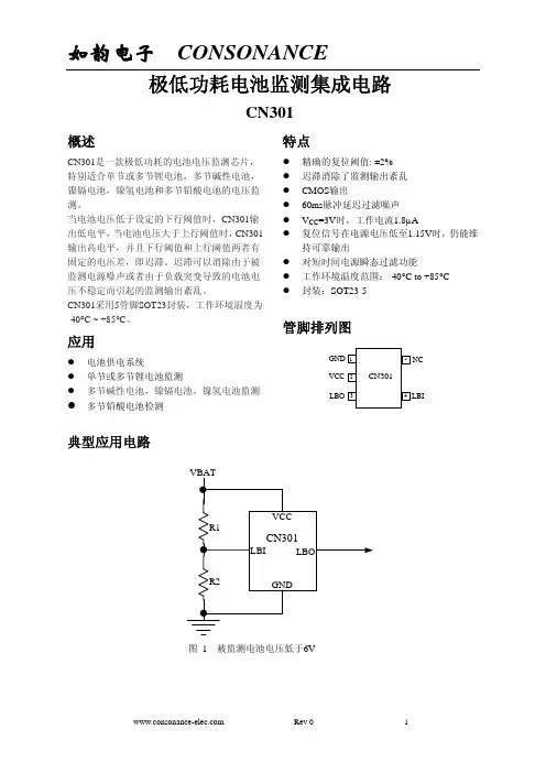
复位IC,电源管理IC系列,替代型号及参数复位ICPJ809 series(2.63/2.93/3.08/4.0/4.38/4.63V)PJ810 series(2.63/2.93/3.08/4.0/4.38/4.63V)PJ705/706/707/708/813EL Driver ICPJ6540C(驱动面积20-40 CM2)PJ6540S(驱动面积20-40 CM2)PJ6540TS(驱动面积20-40 CM2)PJ6543S/TS(驱动面积50-100 CM2)高电压检测ICPJ6101C/NXXXMR series(1.1-6.0V,每隔0.1有型号)LCD Driver ICSC1904(驱动点数19X4)SC1621(驱动点数32X4)SC1621(驱动点数32X4)SC1622(驱动点数32X8)SC1622(驱动点数32X8)SL4808(驱动点数48X8)SC1626(驱动点数48X16)SC1626(驱动点数48X16)SC6523(驱动点数52X3)PJ8566S(驱动点数32X4)小功率AB类音频放大ICPJ4890(1W)PJ4990(1.25W)PJ4871(1.5W)PJ4871(PP)(底部带散热片,1.5W)TDA2822(12V,2X1W)PJ2822(12V,2X1W)TDA2822(9V,2X1W)PJ2822(9V,2X1W)TDA2822(6V,2X1W)LM386中功率AB类音频放大ICPJ4888(2X2.1W,带3D混响功能和立体声耳机功能)PJ4818(2X2.2W,带立体声耳机功能)PJ4088(2X2.2W,带立体声耳机功能)PJ4863MTE(2X2.2W)PJ4863S/P(2X2.2W)CSC4863S(2X2.2W)TEA2025(12V,2X2.5W)TEA2025(9V,2X2.5W)PJ4836(2X2W,带重低音)PJ4836(2X2W,带重低音)TDA7496(2X2W)D1517P(2X4W)TA8227(2X3W)KA2206(2X2.3W)APA2068((2X2.6W,带音量控制,底部带散热片)大功率AB类音频放大ICTDA2030A(18W)LM1875T/L(20W)TDA7265(2X25W)YD7377(2X30W或4X6W)D类音频放大ICPJ2005(1.4W,单声道,D类音频放大)PJ2010(1.3W,单声道,D类音频放大)TPA2012D2(2X1.4W,立体声,D类音频放大)PJ2012(2X1.5W,立体声,D类音频放大)AX2012(2X1.4W,立体声,D类音频放大)PJ8008(2X1.5W,立体声,D类音频放大)耳机音频放大ICPJ4800(2X290mW,立体声耳机放大IC)PJ4808(2X105mW,立体声耳机放大IC)PJ4809(2X105mW,高电平关断,立体声耳机放大IC)PJ8608(2X105mW,立体声耳机放大IC)PJ4880(2X250mW,立体声耳机放大IC)PJ7000(2X40mW,立体声耳机放大IC)LM4853M(2X300mW立体声耳机放大或1.5W单声道耳机放大 IC)全差分AB类音频放大ICPJ4898(全差分,1W)PJA6211(全差分,1.25W)PJA6203(全差分,1.25W)音量音质处理ICCSC2313(三组立体声输入音质处理IC,6V-10V.)CSC2314(四组立体声输入音质处理IC,6V-10V.)D2322(6通道AV前置控制IC,5-12V.)D2323(6通道音响输入选择IC,4.5-12V.)CSC2256(双声道音量控制IC,2.5V-12V.)PT2258(六声道音量控制IC,5V-10V.)M62429(双声道音量控制IC,5V.)TC9153(音量控制IC,4.5-12V.)混响处理ICCD2399单片调频调幅收音ICCD9088(单片电调谐调频收音IC)CD1191(单片调频调幅收音IC)TA2003(单片调频调幅收音IC)YT2111(单片调频调幅立体声收音IC)YD2149(单片调频调幅收音IC/3V工作)并联白灯背光ICPJ7110(并3路白灯,每路20mA)PJ7111(并4路白灯,每路20mA)PJ5920(并3路白灯,每路20mA)PJ5921(并4路白灯,每路20mA)PJ9300(并4路白灯,每路20mA)PJ3200(并5路白灯,每路20mA)PJ2133(并4路白灯,每路可达30mA)PJ60230(并5路白灯,每路可达30mA)PJ9364(并4路白灯,每路可达20mA)PJ9362(并4路白灯,每路可达30mA)PJ9360(并4路白灯,每路可达30mA)PJ3114(并6路白灯,每路20mA)霍尔ICPJ90248S/TPJ177A/B/CPJ1881S/TPJ732S/TPJ211A/B/CTPJ41S/TPJ49ETPJ40APJ5881PJ3144RS232接口ICMAX232锂电保护ICPJ5426AB(4.3V过充保护电压)PJ5426BB(4.28V过充保护电压)PJ2188(4.3V过充保护电压,内置MOS的2合1锂电保护IC)锂电保护板所用MOS管PJ9926SPJ9926TPJ8205T(新版样品)PJ8205MR(新版样品)PJ5N20VPJ8810TPJ8810MRPJ8822TPJ8822MRPJ8818TPJ8818MRPJ8820MRPJ8208PJ6968PJ8209MR单节锂电充电ICPJ4054MR(800mA)PJ4054DR(800mA)PJ4054PR(1A)PJ4056MR(800mA,带双灯指示功能)PJ4060C(250mA,双灯指示功能,其中一个灯为七彩灯指示) PJ4060D(250mA,双灯指示功能)PJ4050S(500mA)PJ2051S(1A)PJ4100(1A)VM7205M/S(1A,须外接场效应管)PJ9501A/B(1A,须外接场效应管,B:4.2V,A:4.1V,一般推B版的)单节锂电/镍氢电池/铅酸电池线性充电ICPJ4062S(500mA,4.2V充满,充电电压可调,也可充镍氢/铅酸电池) PJ4066(1A,4.2V充满,充电电压可调,也可充镍氢/铅酸电池)单节磷酸铁锂电/镍氢电池/铅酸电池线性充电ICPJ4058S(500mA,3.6V充满,充电电压可调,也可充镍氢/铅酸电池) PJ4059(1A,3.6V充满,充电电压可调,也可充镍氢/铅酸电池)开关电源绿色模式PWM控制ICPJ6848M/PPJ6850M/P/SPJ6853M/PPJ6842M/P/SPJ6860(15W)PJ2530A(5W)PJ2603P(6W,内置700V三极管)PJ2604P(6W-8W,内置700V三极管)PJ2605S(3.8W-4.5W,内置700V三极管)PJ2607P(18W,须外加高压功率三极管)PJ8022P(20W以下,内置700VMOS管,输入电压9-38V,耐压50V) PJ8012P(13W以下,内置730VMOS管,输入电压10-39V,耐压50V) PJ1203(5-120W,输入电压耐压16V)I2C实时时钟/日历ICPJ8563S/P/T/MPJ1302S/PAM/FM 频率显示驱动ICSC3610SC3610D马达驱动ICD5898(PDVD 含双路DC-DC 4通道马达驱动IC)D5668(DVD 5通道马达驱动IC)D5868(DVD 5通道马达驱动IC)D5888(DVD 5通道马达驱动IC)D5954(DVD/PDVD/Car DVD/CD机 4通道马达驱动IC)D9258(DVD/PDVD/Car DVD/CD机 4通道马达驱动IC)D9259(DVD/PDVD/Car DVD/CD机 5通道马达驱动IC)YT5901(CD机4通道马达驱动IC)PJ6651AN6650(马达稳速IC)PJ7010R(马达正反转控制驱动IC,1-2A驱动电流)PJ9110(马达正反转控制驱动IC,0.8A驱动电流)PJ9120(马达正反转控制驱动IC,3A驱动电流,须加三级管扩流) PJ9130(直流马达正反转及加速驱动IC,3A驱动电流,须加三级管扩流)锁相环ICAT9256AT9257LC72131电阻式触摸屏控制ICPJ2046PJ2003电容式触摸按键ICTF601(6键输入,工作电压2.5-5.5V)TF401(4键输入,工作电压2.5-5.5V)TF201(2键输入,工作电压2.5-5.5V)TF101(1键输入,工作电压2.5-5.5V)通用运算放大器ICLM324S(四运放/32V)LM324P(四运放/32V)LM324S(四运放/18V)LM324P(四运放/18V)LM358S/P(双运放)JRC4558(双运放)低压运算放大器ICPJ3414(双运放)PJ4510(双运放)PJ2107(单运放)低压低功耗运算放大器ICS324(四运放)S358(双运放)低噪声低失真运算放大器ICPJ4580(双运放)PJ4560(双运放)PJ2568(双运放)大电流运算放大器ICPJ4556(双运放)高带宽高转换速率运算放大器ICPJ2137(双运放)低漂移高精度运算放大器ICOP07(单运放)中频接收ICMC3361通话免提ICMC34018PJ34118PJ34119通话话音网络ICTEA1062/A(A:低电平静噪)压扩电路ICTA31101F(语音压扩电路IC)SL5015(压扩电路IC)SL5020(低压压扩电路IC)DC DC变换ICPJ34063A(1.5A)MC34063B(0.8A)PJ34063(0.8A)三端可调正电源稳压ICLM317L(100mA)LM317T(1.5A)电流型PWM控制ICKA3842S/PKA3843S/P固定频率PWM控制ICKA7500PKA7500STL494PTL494SPJ9741电压比较器ICLM339S(4电压比较器)LM339P(4电压比较器)LM393S/P(双电压比较器)LED显示屏驱动ICPJ62726SS/SO/SP(16位恒流LED驱动IC,每路输出4-90mA) PJ6024(16位恒流LED驱动IC,每路输出3-45mA)LED数码管显示驱动IC(移位寄存器IC)PJ74HC164PJ74HC164PJ74HC595门电路ICPJ74HC244(8路3态缓冲驱动IC)PJ74HC04(六反相器IC)PJ74HC14(六反相施密特触发器IC)SC74HC245(总线驱动双向三态门电路IC)SC74HC138(3-8译码器IC)SC74HC27(四总线收发器IC)SC74HC373(八D锁存器IC)SC74HC393(双4位二进制计数器IC)TFT-LCD 时序控制ICPVI1004DTFT-LCD 信号处理ICD3031LCD视频切换开关ICPI5V330定时器ICNE555立体声D/A转换ICPJ433416位音频D/A转换ICPJ8211CCFL冷光阴极灯控制ICPJ3105恒流恒压控制ICPJ1051MR2A DDR 电源ICPJ9174七路达林顿驱动器阵列ULN2003(七路达林顿驱动器阵列,最大驱动电流可达500MA) ULN2003(七路达林顿驱动器阵列,最大驱动电流可达500MA)模拟开关ICPJ3157(高速单刀双掷模拟开关IC)电源开关ICPJ9701双卡控制ICPJ6188(SPI接口双卡控制IC)4路ESD保护ICPJ3205MRSOT23SOT23SOP8/DIP8 DiceSOP8TSSOP8SOP8/TSSOP8 SOT23DiceDiceSSOP48DiceQFP64DiceDiceQFP100QFP64/LQFP64 LQFP44 MSOP8SMD9(=CSP9) SOP8/DIP8 SOP8(PP)DIP8SOP8DIP8SOP8SOP8/DIP8 SOP8/DIP8 QFN24QFN24QFN16 TSSOP20(PP) SOP16/DIP16 SOP16WSOP16/DIP16 SOP16/DIP16 TSSOP28(PP) HSOP28DIP20/SOP20 DIP18FDIP12SOP16-PPHZIP5TO-220B-5/TO-220-5HZIP11ZIP15QFN8/MSOP8SMD9(=CSP9)/QFN8(=DFN8)QFN20/WCSP16QFN20/WCSP16SOP16WTSSOP20SOP8MSOP8MSOP8SOP8SOP8/DIP8SSOP10MSOP10MSOP10/SMD9(=CSP9)MSOP8/SMD9(=CSP9)SMD9(=CSP9)/QFN8(=DFN8)/MSOP8 SOP28/DIP28SOP28/DIP28SOP28/DIP28SOP28/DIP28SOP16/SOP16WDIP20SOP8/DIP8DIP16DIP16/SOP16SOP16SOP28DIP16/SSOP16SDIP24/SSOP24SDIP24/SSOP24SOT-26MSOP8MSOP8SOT-26SOT-26QFN16QFN16QFN16QFN16QFN16QFN16SOT-23/TO-92 SOT-23/TO-92 SOT-23/TO-92 SOT-23/TO-92 TO-94SOT-23/TO-92 TO-92TO-92/SOT-23 TO-92/SOT-23 TO-92/SOT-23SOP16/DIP16SOT-26SOT-26 TSSOP8SOP8TSOP8TSSOP8 TSSOP6(SOT26) TSSOP8 TSSOP8 TSSOP6(SOT26) TSSOP8 TSSOP6(SOT26) TSSOP8 TSSOP6(SOT26) TSSOP6(SOT26) TSSOP8 TSSOP8 TSSOP6(SOT26) SOT-25DFN10SOT-89-5SOT-26SOT-26SOT-26SOP8SOP8DFN10MSOP8/SOP8MSOP8SOP8DFN10SOP8DFN10SOT-26/DIP8SOT-26/DIP8/SOP8SOT-26/DIP8SOT-26/DIP8/SOP8TO-92TO-92DIP8DIP8SOP8DIP8DIP8DIP8SOP8SOP8/DIP8/TSSOP8/MSOP8 SOP8/DIP8DiceCOB(SOP36)HSOP34HSOP28HSOP28HSOP28HSOP28HSOP28HSOP28QFP44TO-126DIP8SOP8/DIP8SOP8/DIP8SOP8/DIP8DIP16SOP16/DIP16 SOP20/DIP20 DIP22/MFP22QFN16/TSSOP16 TSSOP16SSOP20SOP14SOP8SOP8SOP14DIP14SOP14DIP14SOP8/DIP8 SOP8/DIP8 SOP8/DIP8 SOP8/DIP8 SOT-25/SOP8SOP14/DIP14 SOP8/DIP8 SOP8/DIP8 SOP8/DIP8 SOP8/DIP8SOP8/DIP8SOP8/DIP8SOP8/DIP8SOP16/DIP16SOP28/DIP28 SOP28/DIP28 SOP8/DIP8DIP16SOP16SOP20/DIP20SOP14/DIP14SOP8/DIP8SOP8/DIP8DIP8TO-92TO-220SOP8/DIP8SOP8/DIP8DIP16SOP16DIP16SOP16SSOP16/SOP16SOP14DIP14SOP8/DIP8SSOP24/SOP24/SDIP24 SSOP24/SOP24/QFN24 DIP14(插片)SOP14(贴片)SOP16SOP20SOP14SOP14SOP20SOP16SOP14DIP20DIP14QFP64QFP48SSOP16SOP8/DIP8SOP8/DIP8 SOP8 SSOP20 SOT-26 SOP8DIP16 SOP16 SOT-26 SOT-25 QFN20 SOT-26MAX809/IMP809 seriesMAX810/IMP810 seriesMAX705/706/707/708/813/IMP705/706/707/708/813 series 兼容SM8141兼容SM8141兼容SM8141兼容SM8142XC6101FC(FN)/XC6101CC(CN) seriesHT1621/SL3204HT1621/SL3204HT1622/SL3208HT1622/SL3208HT1623HT1626/SL4816HT1626/SL4816PT6523/SC75823PCF8566LM4890/LM4889/APA0711/NCP2890/PT2366LM4890/LM4889/LM4990/NCP2990LM4871LM4871TDA2822/KA2209TDA2822/KA2209TDA2822/KA2209TDA2822/KA2209TDA2822/KA2209LM386LM4888LM4818/SN4188SN4088/LPA4911LM4863MTELM4863LM4863TEA2025TEA2025LM4836LM4836TDA1517APA2068/G1450TPA2005TPA2010/NCP2820/TS4962/EUA2010/A7013/LM4670/1/3/5/APA2010/PT2333 LM4674TPA2012TPA2012TMPA2155PSTDA1308/LM4800/PT2308/APA4800LM4808LM4809LM4808LM4880/HT82V735FAN7000LM4898/LM4894TPA6211/TPA6204TPA6203PT2313/SC7313PT2314/SC7314PT2322PT2323PT2256PT2258M62429TC9153PT2399TDA9088/TDA7088/TDA1088CXA1191TA2003TA2111TA2149AMC7110AMC7111G5920G5921RT9300LTC3200/AAT3110/RT9361/AAT1501/AIC1848CP2133/FAN5616TPS60230RT9364RT9362RT9360/SC604/CAT3406/PAM2701AAT3114MLX90248/A180/A3212/TLE4913/EW6672ATC177/ATS177US1881EW732/EW512/DN6851FTC211/FTS211SS41/SS400/US1881UA/UGN3175/77UA/UGN3075/77UA/A3132/33/34UA/HAL105/115/125 SS49E/AH41ESS40AUS5881A3144/UGN3140/2/UGS3140/2/A3141/2/3DW01+/CS213/R5426/DW01DW01+/CS213/R5426/DW01兼容CR6002CEM9926/APM9926/AP9926/AO8822/AO8810CEM9926/APM9926/AP9926/AO8822/AO8810CEM8205/APM8205/AP8205/AO8205CEM8205/APM8205/AP8205/AO82055N20VAO8810AO8810AO8822AO8822AO8818AO8818AO8820AO8208APM6968AO8209LTC4054ES5/MCP73831-2(SOT-25)/MCP73832-2(SOT-25)/OCP8020LTC4054ES5/MCP73831-2/MCP73832-2/OCP8020LTC4054ES5/MCP73831-2/MCP73832-2)/OCP8020LTC4054ES5/MCP73831-2(SOT-25)/MCP73832-2(SOT-25)/OCP8020VA7205/VA7202RT9501SG6848/LD7550/OB2262SG6850/LD7550/OB2262/SG5701/SG5848SG6851/LD7535/OB2263/SG6848/SG6849/SG5701/SG5848/LD7550/OB2262/OB2278/OB2279 SG6841/SG6842/LD7552/OB2268/OB2269ACT30/AP3700ACT30/AP3700THX202THX203THX208THX201Viper22Viper12NCP1203PCF8563/PT7C4337DS1302/HT1380/HT1381AM5898AM5668AM5868AM5888BA5954KA9258KA9259BA5901AN6651LG7010LG9110LG9130TC9256/PT9256TC9257/PT9257TSC2046/ADS7846/MT6301/AK4182/ADS7843 TSC2003LM4558/JRC4558NJM3414NJM4510NJM2107SGM324/LMV324SGM358/LMV358NJM4580NJM4560NJM2568NJM4556NJM2137OP07DBL5018/SL5018SC34018MC34118/SC34118MC34119/SC34119SL5015SL5020MC34063AMC34063BLM3842LM3843TL494TL494BA9741/TL1451/SP9741/A1250/AP2001/FP1451 TB62726/MBI5026MBI502474HC16474HC16474HC59574HC24474HC0474HC1474HC24574HC13874HC2774HC37374HC393IR3Y31CS4334PT8211/TDA1311/HT82V731BIT3105TSM1051/SL71051/BD6550G/NJM2336 RT9174ULN2003ULN2003SGM3157RT9701MT6302MAX3205/SRV05-4。
集成电路MM1538应用设计技巧——MITSUMI公司的MM1538应用设计分析MM1538是四通道线性驱动和DC-DC变换控制集成电路,QFP-44脚封装,它是典型的H-桥型驱动方式(BTL),具备较低的功耗,较低的工作电压要求等,特别适合于便携式CD,VCD,MP3播放器的应用。
本文试图通过对MM1538的应用设计分析,探讨一些极具实用价值的典型电路的设计过程,并学习如何读懂集成电路内部框图的含意,理解集成电路内部端口电路的精巧设计。
一、认识MM1538(1)图示MM1538内部功能单元及应用电路(2)管脚功能描述二、功能模块MM1538内部按功能可分为以几个模块:开关机模块、主电源管理模块、伺服驱动模块、电池检测及充电模块,还有部分杂项功能模块。
1、开、关机模块开、关机部分:所谓开机,就是在其第39(START)脚施加“低电平”时(参考应用电路,按开关键)MM1538内部振荡器工作,⑤、37端输出PWM脉冲信号控制DC-DC变换器工作(后面讲述)——系统上电;所谓关机就是在其第40(OFF)脚施加“低电平”时,MM1538内部振荡器停振,⑤、37端不再输出PWM脉冲信号——电路失电,系统恢复到待机状态。
下图分别是39、40的内部电路结构,其中开机电路三极管发射极连接电源BATT——电池电源,而关机电路三极管发射极连接电源是VSYS1,VSYS1是系统上电,DC-DC变换回送到MM1538内部的电源。
为什么这样设计呢?因为当整个系统都没有电源时,开机电路只能使用电池电源;当系统上电后DC-DC变换器工作,产生电源VSYS1,回送到IC内部,所以关机控制电路电源用VSYS1。
反之,若BATT 和VSYS1对调,从图(1)可以看出系统肯定不能开机;从图(2)可以看出电路在待机状态依然有控制作用——这显然不合适!另外,一般来说40脚总是连接MCU 的一个控制端口,待机状态下,控制端口没有电压,电路中有一条放电通路:BATT→IC內部三极管→27K电阻→40脚→MCU的一个控制端口→GND。
ICOM的IC-R71E收信机属于民用接收机,但其接收性能不错,曾经被我国军方侦听站大量配备。
由于它设计定位是民品,没有像军机和高级专业机一样,采用一个高精度基准频率源,而后在它的基础上产生第一本振、第二本振、第三本振、BFO等等机内所需要的信号,而是采用各自为阵的石英晶体振荡器。
由于年代久远,各信号源的频率和幅度早已偏离出厂设定值,造成整机接收性能差。
其实所有的二手老电台和收信机一样,需重新调整才能使其接近出厂状态。
在R71E大量流出之前我就购买到了全模式的、滤波器配备齐全的一级军用收信机WJ-8718/MFP、SSD-009、SD-005A,并拆修研究过IC-751A,因此我没有要收录该机(它没有FM模式,中频滤波器也没配齐,而且没有统一采用一个基准频率源)的任何理由,不过由于该机特别廉价,我常在论坛推荐它。
本文择录于《广播爱好者论坛》,由于该论坛经常发生丢图片的现象,我将它们整理到此地,同时也将会不断搜集其他有关R71E维修方面的资料编辑进来,希望能够对R71E的用户们有用。
几乎所有出厂超过15年的无线电通信设备都存在有一些通病:1、铝电解电容容量降低,内阻增大,少数漏液或者击穿;2、钽电解电容因保存太长时间未通电,突然加额定电压击穿;3、LC槽路垫枕银膜磁管电容银膜硫化或者脱落造成槽路谐振点发生变化;4、低压云母电容和独石电容因贵金属迁移造成短路或者漏电(很可怕,不是关键部位难以发现);5、可调电感的磁芯防松动胶质变质,导致Q值和电感量发生变化;6、如果里边的金属件没有锈蚀迹象,电阻和电感损坏率很低;7、可伐基材镀金的半导体管脚在受潮机器中常出现管脚脆断的现象;8、石英晶体受潮停振;9、晶体管和集成电路损坏;10、普通直插电阻开路性故障;11、按键接触不良;12、电位器碳膜磨损,滑片硫化造成接触不良。
所有这些问题造成出厂已经十多年的旧数字调谐机到手后能够保持出厂性能状态的比例不高,即使到手时是好的,维护费用也较高。
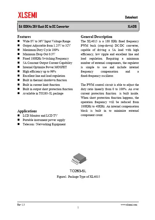

XL4015 5A 降压型直流电源变换器芯片(大功率型 )XL4015 5A 降压型直流电源变换器芯片(大功率型 ) 产品名称: XL4015 5A 降压型直流电源变换器芯片(大功率型 ) 产品型号: XL4015 产品展商:深圳劲锐佳科技有限公司产品文档:无相关文档简单介绍 XL4015 5A 降压型直流电源变换器芯片 (大功率型 ) 1、最大输出电流:5A ;2、最高输入电压: XL4015 为 8~36V 3 、输出电压: ADJ (0.8V) 可调; 4、振动频率: 180kHz ;5、转换效率: 85%~ 95%(不同电压输出时的效率不同);6、控制方式: PWM ;7、工作温度范围: -40℃~ +125℃ 8、工作模式:低功耗/正常两种模式可外部控制; XL4015 5A 降压型直流电源变换器芯片 (大功率型 )1、最大输出电流: 5A ;2、最高输入电压: XL4015 为8~36V3 、输出电压: ADJ (0.8V) 可调;4、振动频率:160kHz ;5、转换效率: 85%~ 95%(不同电压输出时的效率不同);6、控制方式: PWM ; 7、工作温度范围: -40℃~+125℃ 8、工作模式:低功耗 /正常两种模式可外部控制; 9、工作模式控制: TTL 电平兼容; 10、所需外部元件:只需极少的外围器件便可构成高效稳压电路;外围元件少,低纹波。
输入 25V电压,输出 12V 情况下,效率可达到 95%。
12、器件保护:热关断及电流限 ,输出短路保护功能;输入电源开关噪声抑制功能;Enanle 开关信号的迟滞功能;技术特点 (功能兼容 )---AOZ1014,LM2677,LM2678,LM2679 (1)全内置型单片高电压、高频率、高效率、大电流、高可靠性、高性价比集成电路;(2)系统设计简单、方便灵活、高功率密度;( 3)常规的过流保护,过热保护,输出短路保护都内置;(4)高效率,在输入电压 20V-30V ,输出功率 50W 时效率高达90%以上。
元器件交易网TA2131FLGTOSHIBA Bipolar Linear IC Silicon MonolithicTA2131FLGLow Current Consumption Headphone Amplifier for Portable MD Player (With Bass Boost Function)The TA2131FLG is a low current consumption headphone amplifier developed for portable digital audio. It is particularly well suited to portable MD players that are driven by a single dry cell. It also features a built-in bass boost function with AGC, and is capable of bass amplification of DAC output and analog signals such as tuner. An ultra-compact QON package is utilized, enabling sets to be compacted.Features• • • • • • • • • Low current consumption: ICCQ (VCC1) = 0.55 mA (typ.) ICCQ (VCC2) = 0.20 mA (typ.) Output power: Po = 8 mW (typ.) (VCC1 = 2.8 V, VCC2 = 1.2 V, f = 1 kHz, THD = 10%, RL = 16 Ω) Low noise: Vno = −102dBV (typ.) Built-in low-pass boost (with AGC) I/O pin for beep sound Outstanding ripple rejection ratio Built-in power mute Built-in power ON/OFF switch Operating supply voltage range (Ta = 25°C): VCC1 = 1.8~4.5 V VCC2 = 0.9~4.5 VWeight: 0.05 g (typ.) Actual product display name: 213112006-04-19元器件交易网TA2131FLGBlock DiagramVCC1 VCC1 BEEPOFFON PW SWOFFON MT SWOFF ON BST SW BEEP IN 15 BEEP GND Vref IN 13 Vref Vref18 MT TC 19 VCC1 VCC (2.8 V) 20 PW SW171614MUTE SWBOOST SW12LPF1 11 ADD BST NF1 10VrefINB 21 DAC OUT VrefBST1VrefLPF2 22 INA BEEP OUTB BEEP OUTABST2 PW A PW B9 BST NF2 8 BST OUTVref23Vref24BST AGC 1 VCC2 16 OUTA 3 PWR GND 4 OUTB 5 DET 6 AGC IN7+B (1.2 V) RL RL22006-04-19元器件交易网TA2131FLGTerminal Explanation (Terminal voltage: Typical terminal voltage at no signal with testcircuit, VCC1 = 2.8 V, VCC2 = 1.2 V, Ta = 25°C)Terminal No. 1 VCC2 Terminal Explanation VCC (+B) at power amplifier output stage InternaL Circuit ⎯ Terminal Voltage (V) 1.220 kΩ2OUTA Power amplifier output 22 20 kΩ ADDPWA 0.61 220 kΩ4OUTB21INB10 kΩ 10 kΩBST1 OUTBST210 kΩ15 kΩPower amplifier input 20 kΩ 10 kΩ 10 kΩ10 kΩ 7 0.61 10 kΩ 15 kΩ22INA7BST OUTBST amplifier 2 output terminal 21 BST amplifier 2 NF terminal (low-pass compensation condenser connection terminal) GND of power amplifier output stage 20 kΩ PWB40.618BST NF20.61 83PWR GND⎯0205DETSmoothing of boost AGC level detection5.1 kΩ5⎯32006-04-19元器件交易网TA2131FLGTerminal No. Terminal Explanation InternaL Circuit Terminal Voltage (V)20 Signal input level to BST amplifier is varied according to the input level to the boost AGC input terminal. Input impedance: 15 kΩ (typ.)6AGC IN5 kΩVref 0.616 10 kΩADD 20 kΩ20 kΩ9LPF2BST amplifier 1 output (filter terminal) 22PWAAGCBST10.61 BST2 AMP1120 kΩ10 kΩ12 kΩ10BST NF1BST amplifier 1 NF21 PWB 2 kΩ 30 kΩ0.6110 11 LPF1 ADD amplifier output (filter terminal) Vref9 0.61 Vref20 12 Vref Reference voltage circuit 4 kΩ 0.6110 kΩ13Vref INReference voltage circuit filter terminal1310 kΩ12 0.6114GNDGND of input stage in power amplifier⎯042006-04-19元器件交易网TA2131FLGTerminal No. Terminal Explanation Beep sound input terminal Receives beep sound signals from microcomputer. InternaL Circuit Terminal Voltage (V)15BEEP IN20023BEEP OUTB Beep sound output terminal1510 kΩ23 24 ⎯24BEEP OUTA16BST SWBass boost ON/OFF switch “H” level/OPEN: BST ON “L” level: BST OFF Refer to function explanation 520 ⎯20 kΩ 16VCC1 20 17 MT SW Mute switch “L” level: Mute reset “H” level: Mute ON Refer to function explanation 5 17 ⎯ 47 kΩVCC1 20 Power ON/OFF switch “H” level: IC operation “L” level: IC OFF Refer to function explanation 5 47 kΩ 18 ⎯18PW SW52006-04-19元器件交易网TA2131FLGTerminal No. Terminal Explanation InternaL Circuit Terminal Voltage (V)2019MT TCMute smoothing Power mute switch Reduces the shock noise during switching12 kΩ1.21920VCC1Main VCC⎯2.862006-04-19元器件交易网TA2131FLGFunction Explanation1. Bass Boost Function1-1 Description of OperationTA2131FLG has a bass boost function for bass sound reproduction built-in to the power amplifier. With the bass boost function, at medium levels and lower, channel A and channel B are added for the low frequency component, and output to BST amplifier 2 (BST2) in negative phase. That signal is inverted and added before being subjected to bass boost. If the signal of the low-frequency component reaches a high level, the boost gain is controlled to main a low distortion (see Fig.1).20 kΩ INA 20 kΩ 22 10 µF DAC OUT 10 µF Vref 20 kΩ ADD 10 kΩ 20 kΩ 12 kΩ BST1 BST2 2 kΩ 30 kΩ 10 kΩ 20 kΩ 10 kΩ PWB 10 kΩ 15 kΩ 10 kΩ 15 kΩ 10 kΩ PWA 10 kΩ OUTA 2V (OUT) 220 µFV (RL) 16 ΩRL BST NF2 8 1 µF Vref V (NF2) 4 220 µF 16 Ω RL20 kΩBST AGC 10 kΩ5 kΩLPF1 0.1 µF V (LPF1)11 0.1 µFDET 5AGC IN BST NF1 6 10 4.7 µF 0.1 µF V (NF1)9LPF2 V (LPF2)BST OUT 7 0.1 µF 22 kΩ V (BST OUT)VrefVrefVrefFigure 1 System Diagram of Bass Boost1-2AGC CircuitThe AGC circuit of the bass boost function detects with “AGC DET” the voltage component created by “BST2,” and as the input level increases, the variable impedance circuit is changed, and the bass boost signal is controlled so that it is not assigned to BST amplifier 1. In this way, the bass signal to “BST2” input is shut-off, and that boost gain is controlled.1-3Bass Boost SystemAs shown in Fig.1, the flow of the bass boost signal is that the signal received from power amplifier input goes through LPF1, ADD amplifier, ATT (variable impedance circuit), BPF1 (BST amplifier 1) and LPF2, and the negative phase signal to the power amplifier input signal is output from BST amplifier 2. The reason why it becomes the negative phase of the BST amplifier 2 signal is that the phase is inverted by 180° in the audible bandwidth by the secondary characteristics of LPF1 and LPF2 in Fig.1. Ultimately the main signal and the bass boost signal formed before BST2 are added. Fig.2 shows the frequency characteristics to each terminal.10 kΩ OUTBINB 2172006-04-19元器件交易网TA2131FLG40 V (OUT) 20 V (RL) V (NF2) 0 V (LPF2)(dB)V (BST OUT)GV−20V (NF1)−40V (LPF1)−60 1101001k10 k100 kf(Hz)Figure 2 During Bass Boost (Frequency Characteristics to Each Terminal)2. Low-Pass Compensation2-1. FunctionIn C-couple type power amplifiers, it is necessary to give the output condenser C a large capacity to flatten out the frequency characteristics to the low frequency band (this is because the loss in the low frequency bandwidth becomes larger due to the effect of the high-pass filter comprising C and RL). Particularly when the headphone load is approximately 16 Ω and an attempt is being made to achieve frequency characteristics of ±3 dB at 20 Hz, a large capacity condenser of C = 470 µF is required. Bearing this situation in mind, a low-pass compensation function was built in to the TA2131FLG, and while reducing the capacity of the output coupling condenser, almost flat (±3 dB) frequency characteristics in all audible bandwidths (20 Hz to 20 kHz) have been achieved. Fig.3 shows the low-pass system diagram, and Fig.4 shows the frequency characteristics at each point. In Fig.4, (a) represents the status lost by the low-pass as a result of the high-pass filter comprising the headphone load (RL = 16 Ω) and the output coupling condenser (220 µF) in the C-coupling system.20 kΩ INA 20 kΩ 22 10 µF DAC OUT 10 µF 21 INB 20 kΩ 10 kΩ PWB Vref 20 kΩ BST2 10 kΩ 10 kΩ 15 kΩ 10 kΩ 15 kΩ 10 kΩ ADD PWA 10 kΩ OUTA 2V (OUT) V (RL) 220 µF 16 Ω RL BST NF2 8 1 µF Vref 220 µF 16 Ω RL10 kΩ 4 OUTB20 kΩFigure 3 Low-Pass Compensation System Diagram82006-04-19元器件交易网TA2131FLG20 (b)10(dB)(c) 0 (a)GV−10 −20 1101001k10 k100 kf (Hz)Figure 4 Power Amplifier Frequency Characteristics<Principle of Low-Pass Compensation> The low-pass component alone is extracted from the composite signal of PWA/PWB output, and that frequency signal is fed back to PWA/PWB once more via the inversion amplifier, thereby making it possible to increase the gain only of the low-pass component. The frequency characteristics of the power amplifier output V (OUT) in this state are shown in Fig.4 (b). In practice they are the frequency characteristics (c) viewed from load terminal V (RL), and the low-pass is compensated relative to the state in (a).2-2.Low-Pass Compensation Condenser and CrosstalkIn this low-pass compensation condenser circuit, processing is carried out using the composite signal of power amplifier output, so this affects crosstalk, according to the amount of compensation. f characteristics and crosstalk generated by the capacity of the condenser for compensation (8-pin) are shown below.10 VCC1 = 2.8 V VCC2 = 1.2 V Rg = 620 Ω RL = 16 Ω C = 0.47 µF Filter: LPF 80 kHz Output C = 220 µF 0 Vref short C = 1 µF C = 2.2 µFResponse (dB)−10 10301003001k3k10 k30 kf (Hz)Figure 5 Condenser and f Characteristics for Low-Pass Compensation92006-04-19元器件交易网TA2131FLGCT – fVCC1 = 2.8 V VCC2 = 1.2 V Rg = 620 Ω RL = 16 Ω Vo = −22dBV WIDE BAND Output C = 220 µF C = 1 µF0C = 0.47 µFCT (dB)−20 C = 2.2 µF−40 Vrefshort−60 10301003001k3k10 k30 k 100 kf (Hz)Figure 6 Low-Pass Compensation Condenser and Crosstalk3. BeepBeep sound signals from microcomputer can be received by the beep input terminal (15-pin). The PWA and PWB of the power amplifier during power mute are turned OFF, and the beep signal input from BEEP-IN (15-pin) is output from the BEEP-OUT terminal (23/24-pin) as fixed current, after passing through the converter and current amplification stage. Connecting this terminal to the headphone load outputs the beep sound. If the beep sound is not input, fix the BEEP-IN (15-pin) terminal to GND level.VCC PW SW (18-pin) OFF MT SW (17-pin) OFF BEEP IN (15-pin) 200 ms 20 IBEEP 15 IBEEP ID 23 24 100 ms 100 ms ON OFFONOFF4.Power SwitchAs long as the power switch is not connected to “H” level, the IC does not operate. If it malfunctions due to external noise, however, it is recommended to connect a pull-down resistor externally (the power switch is set to be highly sensitive).102006-04-19元器件交易网TA2131FLG5. Threshold Voltages of Switches(1)5 4.5 VPW SW5(2)4.5 VMT SW, BST SW(V)4(V)H43V16 , V17V183 HTerminal voltage2 1.6 V 1 0.6 V L 0 1 2 3 4 5Terminal voltage210.8 V 0.3 V L 2 3 4 501Power supply voltageVCC (V)Power supply voltageVCC (V)PW SW (V18) “H” level “L” level IC operation IC OFF “H” level “L” levelMT SW (V17) Mute ON Mute resetBST SW (V16) “H” level/OPEN “L” level BST ON BST OFF6.These capacitors which prevent oscillation of the power amplifier, and are between the Vref and VCC-GND must have a small temperature coefficient and outstanding frequency characteristics.112006-04-19元器件交易网TA2131FLGAbsolute Maximum RatingsCharacteristic Supply voltage Output current Power dissipation Operating temperature Storage temperature Symbol VCC Io (peak) PD (Note) Topr Tstg Rating 4.5 100 350 −25~75 −55~150 Unit V mA mW °C °CNote: Derated above Ta = 25°C in the proportion of 2.8 mW/°C.Electrical Characteristics (Unless specified otherwise, VCC1 = 2.8 V, VCC2 = 1.2 V,Rg = 600 Ω, RL = 16 Ω, f = 1 kHz, Ta = 25°C)Characteristic Symbol ICC1 ICC2 Quiescent supply current ICC3 ICC4 ICC5 ICC6 Power supply current during drive Gain Channel balance Output power Total harmonic distortion Power Section Output noise voltage Crosstalk ICC7 ICC8 GV CB Po max THD Vno CT RR1 Ripple rejection ratio RR2 Mute attenuation Beep sound output voltage ATT VBEEP BST1 Boost gain BST2 BST3 Test Condition IC off (VCC1), SW1: b, SW2: b IC off (VCC2), SW1: b, SW2: b Mute on (VCC1), SW1: a, SW2: b Mute on (VCC2), SW1: a, SW2: b No signal (VCC1), SW1: a, SW2: a No signal (VCC2), SW1: a, SW2: a Po = 0.5 mW + 0.5 mW output (VCC1) Po = 0.5 mW + 0.5 mW output (VCC2) Vo = −22dBV Vo = −22dBV THD = 10% Po = 1 mW Rg = 600 Ω, Filter: IHF-A, SW4: b Vo = −22dBV fr = 100 Hz, Vr = −20dBV inflow to VCC2 fr = 100 Hz, Vr = −20dBV inflow to VCC1 Vo = −12dBV, SW2: a → b V Beep IN = 2 Vp-o, SW2: b Vo = −20dBV, f = 100 Hz, SW3: ON → OPEN Vo = −30dBV, f = 100 Hz, SW3: ON → OPEN Vo = −50dBV, f = 100 Hz, SW3: ON → OPEN Min ⎯ ⎯ ⎯ ⎯ ⎯ ⎯ ⎯ ⎯ 10 −1.5 5 ⎯ ⎯ −42 −71 −54 −90 −53 1 10 13.5 Typ. 0.1 0.1 0.35 5 0.55 0.20 0.6 5.3 12 0 8 0.1 −102 −48 −77 −64 −100 −48 4 13 16.5 Max 5 5 0.50 10 0.75 0.40 ⎯ ⎯ 14 dB 1.5 ⎯ 0.3 −96 ⎯ ⎯ dB ⎯ ⎯ −43 7 16 19.5 dB dBV mW % dBV mA mA µA Unit µA122006-04-19元器件交易网TA2131FLGTest CircuitVCC VCC Rg = 600 Ω 4.7 µF 15 BEEP IN 14 GND 13 Vref IN V ref(a) (b) SW1 (a)(b) SW2SW3 OFF ON18 1 µF 19 MT TC PW SW17 MT SW16 BST SW1210 µFVCC1 (2.8 V) 600 Ω (b) 10 µF (a) SW4B (a) 10 µF 600 Ω Vref (b) SW4A20 VCC1LPF1 110.1 µFVref21 INB TA2131FLG 22 INABST 10 NF1Vref 4.7 µFLPF2 9 0.1 µF BST NF2Vref23BEEP OUTB8VrefVCC2 1OUTA 2PWR GND 3 (*)OUTB 4DET 5 0.1 µF (*)6220 µF+B (1.2 V)16 Ω220 µF16 Ω(*) 0.22 µF + 10 Ω Monolithic ceramic capacitor22 kΩ0.1 µF24BEEP OUTABST AGC OUT 7 IN132006-04-19元器件交易网TA2131FLGApplication Circuit 1VCC1 VCC1 100 kΩ OFF ON 0.1 µF BEEPOFFONOFFON18 MT TC PW SW1 µF1917 MT SW16 BST SW15 BEEP IN14 GND4.7 µF 13 Vref IN Vref1210 µFVCC (2.8 V)20 VCC1LPF1 110.1 µFVref10 µF DAC OUT 10 µF Vref21 INB TA2131FLGBST 10 NF1Vref 4.7 µF22 INALPF2 90.1 µFVrefBEEP 23 OUT BBST 8 NF21 µFVref+B (1.2 V)220 µFRL220 µFRL0.1 µF(*)(*)(*) 0.22 µF + 10 Ω Monolithic ceramic capacitor22 kΩVCC2 1OUTA 2OUTB 4DET 5360.1 µF24BEEP OUTAPWR GNDBST AGC OUT IN7142006-04-19元器件交易网TA2131FLGApplication Circuit 2 (Low-Pass Compensation/Bass Boost Function/Beep Not Used)VCC1VCC1OFFONOFFON18 MT TC PW SW1 µF1917 MT SW16 BST SW15 BEEP IN14 GND4.7 µF 13 Vref IN Vref 1210 µFVCC1 (2.8 V)20 VCC1LPF1 11Vref10 µF DAC OUT 10 µF Vref21 INB TA2131FLGBST 10 NF122 INALPF2 9Vref23BEEP OUTBBST 8 NF2Vref24BEEP OUTA VCC2 1 OUTA 2 220 µFPWR GND 3OUTB 4 220 µF (*)DET 5BST AGC OUT IN 67(*)+B (1.2 V)Vref RLRL(*) 0.22 µF + 10 Ω Monolithic ceramic capacitor152006-04-19元器件交易网TA2131FLGCharacteristics (Unless otherwise specified VCC1 = 2.8 V, VCC2 = 1.2 V, Rg = 600 Ω,f = 1 kHz, Ta = 25°C)1.0ICC – VCC21.0VDC – VCC2(Vref, OUT)(mA)0.80.8ICCQuiescent supply current0.4Output voltage0.6(V)ICC5 0.6 0.4 0.2 ICC6 0.2 0 0.60.81.01.21.41.61.82.02.22.40 0.60.81.01.21.41.61.82.02.2Supply voltageVCC2(V)Supply voltageVCC2(V)ICC – VCC21.0MUTE ON100Po – VCC2(mA)ICC(mW) Output voltage Po0.83010Quiescent supply current0.630.4ICC310.20.3 ICC4 0 0.6 0.8 1.0 1.2 1.4 1.6 1.8 2.0 2.2 2.4 0.1 0.6 0.8 1.0 1.2 1.4 1.6 1.8THD = 10 % A/Bch IN 2.0 2.2 2.4Supply voltageVCC2(V)Supply voltageVCC2(V)ICC – Po−80Vno – VCC2IHF-A −85 −90 −95 −100 −105 −110 −115 −120 0.6(mW)100ICC30Consumption supply current10ICC831ICC70.30.1 0.01Output noise voltageVno(dBV)A/Bch IN0.030.10.31310300.81.01.21.41.61.82.02.22.4Output voltagePo(mW)Supply voltageVCC2(V)162006-04-19元器件交易网TA2131FLGTHD – Po10 0R.R. – VCC2inflow to VCC1fr = 100 Hz Vr = −20dBV(%)3R.R. (dB)10 kHz−20THD1Total harmonic distortion0.3Ripple rejection ratio3 10 30 100 300−40−600.1 100 Hz/1 kHz 0.03−800.01 0.10.31−100 0.40.81.21.62.02.4Output voltagePo(mW)Supply voltageVCC2(V)THD – VCC230 RL = 16 Ω 0 Po = 1 mW A/Bch INR.R. – VCCinflow to VCC2fr = 100 Hz Vr = −20dBV(%)10(dB) R.R. Ripple rejection ratio2.4−20THD3Total harmonic distortion−401−600.3 1 kHz10 kHz 100 Hz0.1−800.03 0.60.81.01.21.41.61.82.02.2−100 0.40.81.21.62.02.4Supply voltageVCC2(V)Supply voltageVCC2(V)Vo – f0 −10 −30 −40BEEP(dBV)(dBV) Beep output voltage−20 −30 −40 −50 −60 −70 10−50 −60 −70 −80 −90 −100 −110 0.1 fBEEP = 400 Hz rectangle wave 0.3 0.5 1 3 5 10Output voltageVo301003001k3k10 k30 kFrequencyf(Hz)beep input voltageVBEEP(Vp-o)(V)172006-04-19元器件交易网TA2131FLGCT – f0 Vo = −22 dBV 10 1.0ICC – Ta (mA) Quiescent supply current ICC0.8CT (dB)20 Application ciucuit 1 30 40 (No use Low-Pass Compensation) 50 Application ciucuit 2 60 70 100.6ICC5Cross talk0.4ICC6 0.2301003001k3k10 k30 k0 −50−250255075100Frequencyf(Hz)Ambient temperature Ta(°C)VDC – Ta1.0VDC Output voltage(V)0.80.60.40.20 −50−250255075100Ambient temperature Ta(°C)182006-04-19元器件交易网TA2131FLGDisplay of Actual ProductDisplay of Actual Product (Labeling Example) *1*19 *2 0 *1 Display name of actual product: 2131 *2 Weekly Code: 9 0 1 K A Toshiba’s internal management code Weekly code *2 Year (last digit) A K 11-pin displayRequests Concerning Use of QONOutline Drawing of Package(Upper Surface) (Lower Surface)When using QON, please take into account the following items. (1) (2) Do not carry out soldering on the island section in the four corners of the package (the section shown on the lower surface drawing with diagonal lines) with the aim of increasing mechanical strength. The island section exposed on the package surface (the section shown on the upper surface drawing with diagonal lines) must be used as *1 below while electrically insulated from outside. Note 1: Ensure that the island section (the section shown on the lower surface drawing with diagonal lines) does not come into contact with solder from through-holes on the board layout. • • When mounting or soldering, take care to ensure that neither static electricity nor electrical overstress is applied to the IC (measures to prevent anti-static, leaks, etc.). When incorporating into a set, adopt a set design that does not apply voltage directly to the island section.192006-04-19元器件交易网TA2131FLGPackage DimensionsWeight: 0.05 g (typ.)202006-04-192006-04-19 21RESTRICTIONS ON PRODUCT USE 060116EBA• The information contained herein is subject to change without notice. 021023_D • TOSHIBA is continually working to improve the quality and reliability of its products. Nevertheless, semiconductor devices in general can malfunction or fail due to their inherent electrical sensitivity and vulnerability to physical stress. It is the responsibility of the buyer, when utilizing TOSHIBA products, to comply with the standards of safety in making a safe design for the entire system, and to avoid situations in which a malfunction or failure of such TOSHIBA products could cause loss of human life, bodily injury or damage to property.In developing your designs, please ensure that TOSHIBA products are used within specified operating ranges as set forth in the most recent TOSHIBA products specifications. Also, please keep in mind the precautions and conditions set forth in the “Handling Guide for Semiconductor Devices,” or “TOSHIBA Semiconductor Reliability Handbook” etc. 021023_A• The TOSHIBA products listed in this document are intended for usage in general electronics applications (computer, personal equipment, office equipment, measuring equipment, industrial robotics, domestic appliances, etc.). These TOSHIBA products are neither intended nor warranted for usage in equipment that requires extraordinarily high quality and/or reliability or a malfunction or failure of which may cause loss of human life or bodily injury (“Unintended Usage”). Unintended Usage include atomic energy control instruments, airplane or spaceship instruments, transportation instruments, traffic signal instruments, combustion control instruments, medical instruments, all types of safety devices, etc. Unintended Usage of TOSHIBA products listed in this document shall be made at the customer’s own risk. 021023_B• The products described in this document shall not be used or embedded to any downstream products of which manufacture, use and/or sale are prohibited under any applicable laws and regulations. 060106_Q• The information contained herein is presented only as a guide for the applications of our products. No responsibility is assumed by TOSHIBA for any infringements of patents or other rights of the third parties which may result from its use. No license is granted by implication or otherwise under any patent or patent rights of TOSHIBA or others. 021023_C• The products described in this document are subject to the foreign exchange and foreign trade laws. 021023_EAbout solderability, following conditions were confirmed• Solderability(1) Use of Sn-37Pb solder Bath· solder bath temperature = 230°C· dipping time = 5 seconds· the number of times = once· use of R-type flux(2) Use of Sn-3.0Ag-0.5Cu solder Bath· solder bath temperature = 245°C· dipping time = 5 seconds· the number of times = once· use of R-type flux元器件交易网。
低噪声电荷泵DC/DC转换电路概述与特点CSC3301是一个具备低噪声、恒定开关频率(400KHz)的电容式电压倍增器。
输入2.5至4.5V,产生恒定的5V输出电压,最大输出电流能达到250mA。
较少的外部器件(仅有一只自举电容和VIN以及VOUT上的2只旁路电容)使得CSC3301很适合应用于电池供电的小型设备。
本电路采用新的电荷泵架构,保证零负载情况下工作在恒定的开关频率,并同时减少输入和输出纹波。
该电路具有热保护功能,能承受从VOUT到GND的持续短路。
内置的软启动电路能防止启动时产生过大的浪涌电流。
较高的开关频率,可以使用小型的陶瓷电容。
低电流待机电流,小于1uA。
典型特性●固定输出电压5V(±4%)●输入范围:2.5V~5.0V ●输出电流:最大250mA ●低噪声恒定频率工作●自动软启动降低浪涌电流●待机电流小于1uA●短路保护●无电感器件●采用6脚SOT23封装应用举例●白光LED背光源●锂离子电池备份电源●3V到5V转换●智能卡阅读器●PCMCIA本地5V电源引出端功能引脚符号功能描述1 VOUT 电压输出2 GND 地3 EN 待机脚(高有效)4 C~自举电容负端5 VIN 电压输入6 C+ 自举电容正端极限参数参数 符号 数值 单位 输入电压 VIN -0.3~6 V 输出电压 VOUT -0.3~5.6 V 输出短路时间 不定 EN 脚电压 VEN -0.3~5.6 V 输出电流 IOUT 300 mA 工作温度范围 -30℃—85℃℃ 焊接温度(10s ) 300 ℃ 储存温度范围-65~125℃电特性(除非特别说明,EN=VIN ,CIN=COUT=2.2uF ,Tamb=25℃)参数名称 符号 测试条件规范值单位 最小 典型 最大 输入电压 VIN2.5 5.5 V 输出电压 VOUT 2.7V<VIN<5.5V ,IOUT<65mA 4.7 5 5.2V 待机电流 Ishut EN=0V ,VOUT=0V 0.3uA 空载输入电流 Ino_load IOUT=0mA ,VIN=2.7V0.65 mA 最大输出电流 Iout_max 250 mA 输出纹波 VR VIN=2.7V ,IOUT=100mA 150 Mvp-p 效率 VIN=2.7V ,IOUT=100mA81 % 开环输出电阻IOUT VOUTVIN 2ROL VIN=2.7V ,IOUT=100mA4 Ω 开关频率Fosc400KHz典型特性曲线图典型应用图2.2u F 2.2u F2.2u FC-C+VIN2.7V-5VGNDENVOUT523146OFF/ON5V标准5V输出原理图CSC3301应用信息工作原理CSC3301采用开关电容充电泵来将输入电压提升至恒定输出电压,这个恒定值是根据误差信号,由内置电阻分压器以及电荷泵电流的调节获得的。
背景
目前许多电子产品的供电电源为低压单电源,当电路板中需要为运算放大器等模拟电路提供正负电源时,就需要进行单电源转正负电源的设计。
本文档介绍了基于TI电源转换芯片TPS65130,将输入电压:2.7V~5.5V,转换为±5V~±15V的设计。
电路设计
电路图如上图所示,由电路图可知TPS5130集成两路独立的Boost电路,分别为正极型和负极型。
而目前较多的低成本设计如下图所示,采用一路反馈,另外一路负压是不在控制器的调节之中,电压不稳定、纹波大。
电路特点
●输入:2.7V~5.5V
●输出:±5V~±15V可调
●过压保护、过流保护、过热保护
●工业级、集成度高
输出电流曲线
输出电压调节方法
可通过调节电路反馈电阻比值,来调节输出电压。
反馈电阻采用0603封装。
输出电压调节方法:
V+=(1+R1+R6
R2
)∗1.213
V− =−R5+R7
R3
∗1.213
PCB设计
总结
采用TPS65130设计的单电源转正负电源,具有集成度高、尺寸小、性能优越等特定,能够充分满足在单电源、低电压的供电场所,用于产生高压正负电源,用于给模拟电路等提供双路电源。
CSC3301中⽂资料⽆感升压5V低噪声电荷泵DC/DC转换电路概述与特点CSC3301是⼀个具备低噪声、恒定开关频率(400KHz)的电容式电压倍增器。
输⼊2.5⾄4.5V,产⽣恒定的5V输出电压,最⼤输出电流能达到250mA。
较少的外部器件(仅有⼀只⾃举电容和VIN以及VOUT上的2只旁路电容)使得CSC3301很适合应⽤于电池供电的⼩型设备。
本电路采⽤新的电荷泵架构,保证零负载情况下⼯作在恒定的开关频率,并同时减少输⼊和输出纹波。
该电路具有热保护功能,能承受从VOUT到GND的持续短路。
内置的软启动电路能防⽌启动时产⽣过⼤的浪涌电流。
较⾼的开关频率,可以使⽤⼩型的陶瓷电容。
低电流待机电流,⼩于1uA。
典型特性●固定输出电压5V(±4%)●输⼊范围:2.5V~5.0V ●输出电流:最⼤250mA ●低噪声恒定频率⼯作●⾃动软启动降低浪涌电流●待机电流⼩于1uA●短路保护●⽆电感器件●采⽤6脚SOT23封装应⽤举例●⽩光LED背光源●锂离⼦电池备份电源●3V到5V转换●智能卡阅读器●PCMCIA本地5V电源引出端功能引脚符号功能描述1 VOUT 电压输出2 GND 地3 EN 待机脚(⾼有效)4 C~⾃举电容负端5 VIN 电压输⼊6 C+ ⾃举电容正端极限参数参数符号数值单位输⼊电压 VIN -0.3~6 V 输出电压 VOUT -0.3~5.6 V 输出短路时间不定 EN 脚电压 VEN -0.3~5.6 V 输出电流 IOUT 300 mA ⼯作温度范围 -30℃—85℃℃焊接温度(10s ) 300 ℃储存温度范围-65~125℃电特性(除⾮特别说明,EN=VIN ,CIN=COUT=2.2uF ,Tamb=25℃)参数名称符号测试条件规范值单位最⼩典型最⼤输⼊电压 VIN2.5 5.5 V 输出电压 VOUT 2.7VV 待机电流 Ishut EN=0V ,VOUT=0V 0.3uA 空载输⼊电流 Ino_load IOUT=0mA ,VIN=2.7V0.65 mA 最⼤输出电流 Iout_max 250 mA 输出纹波 VR VIN=2.7V ,IOUT=100mA 150 Mvp-p 效率 VIN=2.7V ,IOUT=100mA 81 % 开环输出电阻IOUT VOUTVIN 2ROL VIN=2.7V ,IOUT=100mA4 Ω开关频率Fosc400KHz典型特性曲线图典型应⽤图2.2u F 2.2u F2.2u FC-C+VIN2.7V-5VGNDENVOUT523146OFF/ON5V标准5V输出原理图CSC3301应⽤信息⼯作原理CSC3301采⽤开关电容充电泵来将输⼊电压提升⾄恒定输出电压,这个恒定值是根据误差信号,由内置电阻分压器以及电荷泵电流的调节获得的。
LCD电源芯片代换TEA1532A EA1532A可以直接代换EA1532C代换EA1532A先看8脚是空脚的外加300伏(我亲自试过的)。
EA1532A代换EA1530A只要将ea1530a的第五脚接到ea1532a原来脚位的第六脚.第六脚接第七脚,第七脚接第五脚位置就OK!1.2.3.4.8脚一样.CQ1265RT 3脚启动电压是18v 5Q1265RT 3脚需要23v电压CQ0765RT 5Q0765RT CQ1465CQ可以直接代换7552=SG68411200AP40与1200AP60 1203P60代换SG5841与DAP02ALSZ可以用SG6841FAN7601与LAF0001可以直接代换EA1532A可以用DAP8AOCP5001-TL5001直接代换AMC3100-LTC3406/A T1366/直接代换MP2104 OCP2150-LTC3406/直接代换AT1366/MP2104 直接代换ACT6906-LTC3406/AT1366/直接代换MP2104 OCP2160-LTC3407直接代换ACT4065-ZA3020/MP1580 直接代换AMC2596-LM2596 OCP1451直接代换TL1451/BA9741/SP9741/AP200直接代换电源IC STR-G5643D G5653D G8653D 直接代换203D6和DAP8A 直接代换1200AP40和1200AP60直接代换5S0765和DP104、DP704直接代换DP804和DP904直接代换2S0680和2S0880直接代换BENQ 71G+ 1200AP40 直插1200AP10 1200AP604 直接代换TEA1507和TEA1533直接代换三星的DP104,704,804可以用5S0765代换,DP904不能用任何块代换电源IC(ZSTR-G5643D G5653D G8653D 直接代换203D6/1203P6和DAP8A 直接代换DM0465R。
1Aug. 2006 Rev. 1. 0BCD Semiconductor Manufacturing LimitedGeneral DescriptionThe AP3015/A are Pulse Frequency Modulation (PFM) DC/DC converters. These two devices are func-tionally equivalent except the switching current limit.The AP3015 is designed for higher power systems with 350mA current limit, and the AP3015A is for lower power systems with 100mA current limit.The AP3015/A feature a wide input voltage. The oper-ation voltage is ranged from 1.2Vto 12V (1V to 12V for AP3015A). A current limited, fixed off-time con-trol scheme conserves operating current, resulting in high efficiency over a broad range of load current.They also feature low quiescent current, switching cur-rent limiting, low temperature coefficient, etc.Fewer tiny external components are required in the applications to save space and lower cost.Furthermore, to ease its use in differnet systems, a dis-able terminal is designed to turn on or turn off the chip.The AP3015/A are available in SOT-23-5 package.Features·Low Quiescent CurrentIn Active Mode (Not Switching): 17µA Typical In Shutdown Mode: <1µA ·Low Operating V IN1.2V Typical for AP3015 1.0V Typical for AP3015A ·Low V CESAT Switch200mV Typical at 300mA for AP3015 70mV Typical at 70mA for AP3015A ·High Output V oltage: up to 34V ·Fixed Off-Time Control ·Switching Current Limiting 350mA Typical for AP3015 100mA Typical for AP3015A·Operating Temperature Range: -40o C to 85o CApplications·MP3, MP4·Battery Power Supply System ·LCD/OLED Bias Supply ·Handheld Device·Portable Communication DeviceFigure 1. Package Type of AP3015/ASOT-23-52Aug. 2006 Rev. 1. 0BCD Semiconductor Manufacturing LimitedFigure 2. Pin Configuration of AP3015/A (Top View)Pin DescriptionPin NumberPin Name Function1SW Switch Pin. This is the collector of the internal NPN power switch. Minimize the trace area connected to this Pin to minimize EMI2GND Ground Pin. GND should be tied directly to ground plane for best performance3FBFeedback Pin. Set the output voltage through this pin. The formula is V OUT=1.23V*(1+R1/R2). Keep the loop between V out and FB as short as possible to minimize the ripple and noise,which is beneficial to the stability and output ripple4SHDN Shutdown Control Pin. Tie this pin above 0.9V to enable the device. Tie below 0.25V to turn off the device5V INSupply Input Pin. Bypass this pin with a capacitor as close to the device as possiblePin ConfigurationK Package (SOT-23-5)SW FBV INSHDNGND3Aug. 2006 Rev. 1. 0BCD Semiconductor Manufacturing LimitedSHDNV INBCD Semiconductor's Pb-free products, as designated with "E1" suffix in the part number, are RoHS compliant.Ordering InformationPackageTemperature RangePart NumberMarking IDPacking TypeSOT-23-5-40 to 85o CAP3015KTR-E1E6E Tape & Reel AP3015AKTR-E1E6FTape & ReelCircuit Type Package E1: Lead Free AP3015TR: Tape and Reel K: SOT-23-5-Blank: AP3015A: AP3015AFunctional Block DiagramFBFigure 3. Functional Block Diagram of AP3015/A4Aug. 2006 Rev. 1. 0BCD Semiconductor Manufacturing LimitedNote 1: Stresses greater than those listed under "Absolute Maximum Ratings" may cause permanent damage to the device. These are stress ratings only, and functional operation of the device at these or any other conditions beyond those indicated under "Recommended Operating Conditions" is not implied. Exposure to "Absolute Max-imum Ratings" for extended periods may affect device reliability.ParameterSymbolMinMaxUnitInput V oltageV INAP3105 1.212VAP3105A1.012Operating TemperatureT A-4085o CRecommended Operating ConditionsAbsolute Maximum Ratings (Note 1)Parameter Symbol Value Unit Input V oltage V IN 15V SW V oltage V SW 36V FB V oltage V FB V IN V SHDN Pin V oltageV SHDN 15V Thermal Resistance (Junction to Ambient, no Heat sink) R θJA 265oC/WOperating Junction Temperature T J 150o C Storage Temperature Range T STG -65 to 150o C Lead Temperature (Soldering, 10sec)T LEAD260o CESD (Human Body Model)3000V5Aug. 2006 Rev. 1. 0BCD Semiconductor Manufacturing Limited(V IN =V SHDN =1.2V , T A =25o C, unless otherwise specified.)Parameter Symbol Conditions Min TypMax Unit Input V oltageV INAP3015 1.212VAP3015A 1.012Quiescent Current I Q Not Switching 1730µA V SHDN =0V1Feedback V oltage V FB 1.2051.23 1.255V FB Comparator Hysteresis V FBH 8mV FB Pin Bias CurrentI FB V FB =1.23V 3080nA Output V oltage Line Regulation L NR 1.2V <V IN <12V 0.050.1%/V Switching Current LimitI LAP3015300350400mA AP3015A75100125Switch Saturation V oltage V CESATAP3015, I SW =300mA 200300mVAP3015A, I SW =70mA 70120Switch Off TimeT OFF V FB >1V 400nS V FB <0.6V1.5µS SHDN Input Threshold High V TH 0.9V SHDN Input Threshold Low V TL 0.25SHDN Pin Current I SHDN V SHDN =1.2V 23µAV SHDN =5V 812Switch Leakage CurrentI SWLSwitch Off, V SW =5V0.015µA Electrical CharacteristicsTypical Performance CharacteristicsUnless otherwise noted, V IN=1.2VFigure 4. Quiescent Current vs. Junction Temperature Figure 5. Feedback Voltage vs. Junction TemperatureFigure 6. Switch Off Time vs. Junction Temperature Figure 7. Shutdown Pin Current vs. Shutdown Pin VoltageAug. 2006 Rev. 1. 0BCD Semiconductor Manufacturing Limited67Aug. 2006 Rev. 1. 0BCD Semiconductor Manufacturing LimitedFigure 9. Switch Current Limit vs. Junction TemperatureTypical Performance Characteristics (Continued)Figure 10. Saturation Voltage vs. Junction Temperature Figure 11. Saturation Voltage vs. Junction TemperatureFigure 8. Switch Current Limit vs. Junction Temperature Unless otherwise noted, V IN =1.2V8Aug. 2006 Rev. 1. 0BCD Semiconductor Manufacturing LimitedFigure 13. EfficiencyTypical Performance Characteristics (Continued)Figure 12. Efficiency Unless otherwise noted, V IN =1.2VApplication InformationOperating PrinciplesAP3015/A feature a constant off-time control scheme.Refer to Figure 3, the bandgap voltage V REF (1.23V typical) is used to control the output voltage. When the voltage at the FB pin drops below the lower hysteresis point of Feedback Comparator (typical hysteresis is 8mV), the Feedback Comparator enables the chip and the NPN power switch is turned on, the current in the inductor begins to ramp up and store energy in the coil while the load current is supplied by the output capacitor. Once the current in the inductor reaches the current limit, the Current-Limit Comparator resets the 400ns One-Shot which turns off the NPN switch for 400ns. The SW voltage rises to the output voltage plus a diode drop and the inductor current begins to ramp down. During this time the energy stored in the inductor is transferred to C OUT and the load. After the 400ns off-time, the NPN switch is turned on and energy will be stored in the inductor again.This cycle will continue until the voltage at FB pin reaches 1.23V , the Feedback Comparator disables the chip and turns off the NPN switch. The load current is then supplied solely by output capacitor and the output voltage will decrease. When the FB pin voltage drops below the lower hysteresis point of Feedback Comparator, the Feedback Comparator enables the device and repeats the cycle described previously.Under not switching condition, the I Q of the device is about 17µA.The AP3015/A contain additional circuitry to provide protection during start-up or under short-circuit conditions. When the FB pin voltage is lower than approximately 0.6V , the switch off-time is increased to 1.5µs and the current limit is reduced to about 250mA (70mA for AP3015A). This reduces the average inductor current and helps to minimize the power dissipation in the AP3015/A power switch, in the external inductor and in the diode.The SHDN pin can be used to turn off the AP3015/A and reduce the I Q to less than 1µA. In shutdown mode the output voltage will be a diode drop below the input voltage.Typical ApplicationC1, C2: X5R or X7R Ceramic CapacitorL1: SUMIDA CDRH4D16FB/NP-100MC or EquivalentFigure 14. AP3015 Typical Application in LCD/OLED Bias SupplyC1, C2, C3: X5R or X7R Ceramic CapacitorL1: SUMIDA CDRH4D16FB/NP-100MC or EquivalentFigure 15. AP3015A Typical Application in 1 or 2 Cells to 3.3V Boost ConverterAug. 2006 Rev. 1. 0BCD Semiconductor Manufacturing Limited9Mechanical DimensionsSOT-23-5Unit: mm(inch)Aug. 2006 Rev. 1. 0BCD Semiconductor Manufacturing Limited10IMPORTANT NOTICEBCD Semiconductor Manufacturing Limited reserves the right to make changes without further notice to any products or specifi-cations herein. BCD Semiconductor Manufacturing Limited does not assume any responsibility for use of any its products for any particular purpose, nor does BCD Semiconductor Manufacturing Limited assume any liability arising out of the application or use of any its products or circuits. BCD Semiconductor Manufacturing Limited does not convey any license under its patent rights or other rights nor the rights of others.- Wafer FabShanghai SIM-BCD Semiconductor Manufacturing Limited 800, Yi Shan Road, Shanghai 200233, China Tel: +86-21-6485 1491, Fax: +86-21-5450 0008BCD Semiconductor Manufacturing LimitedMAIN SITEREGIONAL SALES OFFICEShenzhen OfficeShanghai SIM-BCD Semiconductor Manufacturing Co., Ltd. Shenzhen Office Advanced Analog Circuits (Shanghai) Corporation Shenzhen OfficeRoom E, 5F, Noble Center, No.1006, 3rd Fuzhong Road, Futian District, Shenzhen 518026, China Tel: +86-755-8826 7951, Fax: +86-755-8826 7865Taiwan OfficeBCD Semiconductor (Taiwan) Company Limited 4F, 298-1, Rui Guang Road, Nei-Hu District, Taipei, TaiwanTel: +886-2-2656 2808, Fax: +886-2-2656 2806USA OfficeBCD Semiconductor Corporation 3170 De La Cruz Blvd., Suite 105, Santa Clara,CA 95054-2411, U.S.A- IC Design GroupAdvanced Analog Circuits (Shanghai) Corporation 8F, Zone B, 900, Yi Shan Road, Shanghai 200233, China Tel: +86-21-6495 9539, Fax: +86-21-6485 9673BCD Semiconductor Manufacturing Limited。