ch6 集成运放
- 格式:ppt
- 大小:3.05 MB
- 文档页数:100
![ch6_11_鉴频器原理与电路(4) [兼容模式]](https://img.taocdn.com/s1/m/854fc847e55c3b3567ec102de2bd960590c6d97c.png)
通信电子线路鉴频器原理与电路
(4)
——讲述了脉冲计数鉴频器及本
章小结
利用计数过零脉冲数目的方法实现鉴频。
放大限幅
c 微分
d
削波e脉冲发生器
五. 脉冲计数式鉴频器:方框图和波形图如图:
•经处理后得到幅度相同的矩形脉冲,如图(f)
•对给定的单一频率,这些脉冲具有恒定的平均值,其平均值与FM波的频率成正比。
•输入调频波时,平均幅度随频率的变化规律(调制信号)而线性变化。
•滤波器去掉无用成分就可得到原调制信号。
•优点:
解调失真小;便于集成。
缺点:
•工作频率较低(受限于脉冲发生器的分辨率)。
•若能生成的最小脉冲为τmin,则f max=(f c+∆f f)<1/τmin
本章小结
1.角度调制/解调的基本原理和调角波的性质。
2.调频方法及实现电路。
3.各种调制方式的比较。
4.鉴频器指标、原理电路及其优缺点:
•单端斜率鉴频器:电路简单,线性范围窄;
•平衡斜率鉴频器:线性范围宽,B大,失真小,难调对称;•相位鉴频器:简单、线性好,灵敏度↑,B小;
•比例鉴频器:可省去限幅器,但灵敏度↓;
•符合鉴频器:S/N高、易集成,线性范围窄,灵敏度↓;•脉冲计数器:失真小,易集成,工作f↓。
运放分类工艺
运放按照工艺的分类可以分为以下几种:
1. 单管运放(Single-Ended Amplifier):只有一个输入信号与一个输出信号的运放,常见的有共射放大器和共源放大器等。
2. 双差分运放(Fully-Differential Amplifier):有两个输入信号与两个输出信号的运放,常用于高性能模拟信号处理器件中。
3. 运算放大器(Operational Amplifier):用于数学运算、信号放大和滤波等应用。
4. 功率放大器(Power Amplifier):能够根据输入信号放大电流或电压的运放,常用于音频和功率放大应用中。
5. 低噪声放大器(Low-Noise Amplifier):能够在高增益下提供低噪声的运放,常用于射频和通信系统中。
6. 高速放大器(High-Speed Amplifier):能够在高频率下提供高增益的运放,常用于高速数据传输和信号处理中。
7. 超低功耗放大器(Ultra-Low Power Amplifier):能够在低功耗下提供放大功能的运放,常用于电池供电的便携设备中。
除了以上分类,运放还可以按照工作原理、结构设计和制造工艺等细分。
不同的分类适用于不同的应用场景和需求。

模电Ch1 常用半导体器件基础概念6二极管PN结...PN结和二极管区别2IV特性4主要参数1瞬态响应3IV特性等效电路16微变等效电路7稳压二极管14其他二极管2BJT双极型三极管(Bipolar Junction Transistor,简称BJT)双极: 在工作时有电子和空穴两种载流子参与导电过程注意集电极的结面积较大:为什么要大?为什么是电流控制器件因为β化简成了一个系数,IC和IB成比例4晶体管内部载流子的运动6共射电流放大系数7共射特性曲线输入特性曲线输入特性曲线开启电压Von硅三极管的Von为0.5~0.7V,锗三极管的Von为0.2~0.3V。
指数关系当Uc增大时,曲线将右移输出特性曲线UBE<UEBQ,B-E反偏,B-C反偏开启电压UonB-E正,B-C反偏B-E正,B-C正注意横线由IB控制,而EFT是电压Vgs具体公式是什么?没有吗?这里Ib和纵轴Ic是线性关系,比例为β改变β的方法在半导体器件有讲硅三极管开始进入饱和区的Vce值约为0.6~0.7V例题主要参数17温度对晶体管的影响10FET单极型器件:只靠多数载流子导电结型FET52绝缘栅FET(MOSFET)50主要参数27FET和BJT的比较7集成电路中的元件Ch2 基本放大电路放大电路性能指标28BJT共射放大电路基本共射放大电路6直接耦合共射放大电路8阻容耦合共射放大电路4PNP共射放大电路放大电路分析...静态工作点的稳定温度34BJT放大电路三种基本接法50EFT放大电路55复合管52Ch3 集成运算放大电路使用原因26结构87电压传输特性7零点漂移15主要性能指标1运放类型7集成运放结构拆分11运放等效电路(低频)6运放保护措施7常用结构输入级常使用共集共基来提高输入电阻,提高带宽为什么提高带宽?利用有源负载提高放大倍数,使单端输出电路的差模放大倍数近似等于双端输出电路的差模放大倍数?例题4Ch4 放大电路的频率响应基本高低通模型7晶体管的高频等效模型晶体管的混合π模型简化的混合π模型13β和α随频率的变化10FET的高频等效模型7单管放大电路的频率响应电容考虑情况3单管共射放大电路46单管共源放大电路6频率响应的改善减小fL加大耦合电容及其回路电阻,以增大回路时间常数或各级之间采用直接耦合(不用耦合电容也就没有高通)增大fH减小C'π/C'gs, 而C'π≈Cπ+(gm*RL)Cu,所以可以通过减小gmRL的方法提高fH->注意:fH的提高与|A|的增大是相互矛盾的。


南京凌鸥创芯电子有限公司LKS32MC08X Datasheet© 2020, 版权归凌鸥创芯所有机密文件,未经许可不得扩散1概述1.1功能简述LKS32MC08X系列MCU是32位内核的面向电机控制应用的专用处理器,集成了常用电机控制系统所需要的所有模块。
⚫性能➢96MHz 32位Cortex-M0内核➢集成自主指令集电机控制专用DSP➢超低功耗休眠模式,低功耗休眠电流10uA➢工业级工作温度范围➢超强抗静电和群脉冲能力⚫工作范围➢ 2.2V~5.5V电源供电,内部集成1个LDO,为数字部分电路供电➢工作温度: -40~105℃,LKS32MC085工作温度: -40~125℃⚫时钟➢内置4MHz高精度RC时钟,-40~105℃范围内精度在±1%之内➢内置低速32KHz 低速时钟,供低功耗模式使用➢可外挂4MHz外部晶振➢内部PLL可提供最高96MHz时钟⚫外设模块➢两路UART➢一路SPI,支持主从模式➢一路IIC,支持主从模式➢一路CAN(部分型号不带CAN)➢2个通用16位Timer,支持捕捉和边沿对齐PWM功能➢2个通用32位Timer,支持捕捉和边沿对齐PWM功能;支持正交编码输入,CW/CCW输入,脉冲+符号输入➢电机控制专用PWM模块,支持8路PWM输出,独立死区控制➢Hall信号专用接口,支持测速、去抖功能➢硬件看门狗➢最多4组16bit GPIO。
P0.0/P0.1/P1.0/P1.1 4个GPIO可以作为系统的唤醒源。
P0.15 ~ P0.0 共16个GPIO可以用作外部中断源输入。
⚫模拟模块➢集成1路12bit SAR ADC,同步双采样,3Msps采样及转换速率,最多支持13通道➢集成4路运算放大器,可设置为差分PGA模式➢集成两路比较器,可设置滞回模式➢集成12bit DAC 数模转换器➢内置±2℃温度传感器➢内置1.2V 0.5%精度电压基准源➢内置1路低功耗LDO和电源监测电路➢集成高精度、低温飘高频RC时钟➢集成晶体起振电路1.2性能优势➢高可靠性、高集成度、最终产品体积小、节约BOM成本;➢内部集成4路高速运放和两路比较器,可满足单电阻/双电阻/三电阻电流采样拓扑架构的不同需求;➢内部高速运放集成高压保护电路,可以允许高电压共模信号直接输入芯片,可以用最简单的电路拓扑实现MOSFET电阻直接电流采样模式;➢应用专利技术使ADC和高速运放达到最佳配合,可处理更宽的电流动态范围,同时兼顾高速小电流和低速大电流的采样精度;➢整体控制电路简洁高效,抗干扰能力强,稳定可靠;➢单电源2.2V~5.5V供电,确保了系统供电的通用性;适用于有感BLDC/无感BLDC/有感FOC/无感FOC及步进电机、永磁同步、异步电机等控制系统。

菜鸟进阶必看! 主流音频运放芯片分析运算放大器(简称“运放”)是运用得非常广泛的一种线性集成电路,而且种类繁多,在运用方面不但可对微弱信号进行放大,还可做为反相、电压跟随器,可对电信号做加减法运算,所以被称为运算放大器。
不但其他地方应用广泛,在音响方面也使用得最多。
例如前级放大、缓冲,耳机放大器除了有部分使用分立元件,电子管外,绝大部分使用的还是集成运算放大器。
而有时候还会用到稳压电路上,制作高精度的稳压滤波电路。
各种运放由于其内部结构的不同,产生的失真成分也不同,所以音色特点也有一定的区别。
本来我们追求的是高保真,运放应该是失真最低,能真实还原音乐,没有个性的最好。
但是由于要配合其他音响部件如数码音源、后级功放管等,如果偏干、偏冷则可搭配音色细腻温暖型的运放,而太过阴柔、偏软的则可搭配音色较冷艳、亮丽的运放,做到与整机配合,取长补短的最佳效果。
所以说,并不是选择越贵的运放得到的效果就一定越好,搭配很重要,达到听感上最好才算达到目的。
如果是应用在低电压的模拟滤波电路中,还要选择对低电压工作性能良好的运放种类。
市面上的运放种类不下五六百种,GBW带宽在5M以上的也有三百多种,最高的已达300MHZ,转换速率在5V/us以上的也不下几百种,最高达3000V/us。
低档运放JRC4558,这种运放是低档机器使用得最多的。
现在被认为超级烂,因为它的声音过于明亮,毛刺感强,所以比起其他的音响用运放来说是最差劲的一种。
不过它在我国暂时应用得还是比较多的,很多的四、五百元的功放还是选择使用它,因为考虑到成本问题和实际能出的效果,没必要选择质量超过5532以上的运放。
对于一些电脑有源音箱来说,它的应付能力还是绰绰有余的。
5532,如果有谁还没有听说过它名字的话,那就还未称得上是音响爱好者。
这个当年有运放皇之称的NE5532,与LM833、LF353、CA3240一起是老牌四大名运放,不过现在只有5532应用得最多。

常见集成运放型号大全LF351 BI-FET单运算放大器NSLF353 BI-FET双运算放大器NSLF356 BI-FET单运算放大器NSLF357 BI-FET单运算放大器NSCA3130高输入阻抗运算放大器IntersilCA3140 高输入阻抗运算放大器CD4573 四可编程运算放大器MC14573ICL7650斩波稳零放大器LF347(NS[DATA]) 带宽四运算放大器KA347LF398 采样保持放大器NS[DATA]LF411 BI-FET单运算放大器NS[DATA]LF412 BI-FET双运放大器NS[DATA]LM318 高速运算放大器NS[DATA]LM324四运算放大器NS[DATA]HA17324,/LM324(TI)LM348四运算放大器NLM358NS[DATA] 通用型双运算放大器HA17358/LM358P(TI)LM380 音频功率放大器NS[DATA]LM386-1 NS[DATA] 音频放大器NJM386D,UTC386LM386-3 音频放大器NS[DATA]LM386-4 音频放大器NS[DATA]LM3886 音频大功率放大器NS[DATA]LM3900 四运算放大器LM124 低功耗四运算放大器(军用档) NS[DATA]/TI[DATA]LM1458 双运算放大器NS[DATA]LM148 四运算放大器NS[DATA]LM224J 低功耗四运算放大器(工业档) NS[DATA]/TI[DATA]LM2902 四运算放大器NS[DATA]/TI[DATA]LM2904 双运放大器NS[DATA]/TI[DATA]LM301 运算放大器NS[DATA]LM308 运算放大器NS[DATA]LM308H 运算放大器(金属封装)NS[DATA]LM725 高精度运算放大器NS[DATA]LM733 带宽运算放大器LM741 NS[DATA] 通用型运算放大器HA17741TBA820M 小功率音频放大器ST[DATA]TL061 BI-FET单运算放大器TI[DATA]TL062 BI-FET双运算放大器TI[DATA]TL064 BI-FET四运算放大器TI[DATA]TL072 BI-FET双运算放大器TI[DATA]TL074 BI-FET四运算放大器TI[DATA]TL081 BI-FET单运算放大器TI[DATA]TL082 BI-FET双运算放大器TI[DATA]TL084 BI-FET四运算放大器TI[DATA]MC34119 小功率音频放大器NE592 视频放大器OP07-CP精密运算放大器TI[DATA]OP07-DP 精密运算放大器TI[NE5532 高速低噪声双运算放大器TI 双运放NE5534 高速低噪声单运算放大器TI 单运放OPA602 高速高精度运放(无OPA2602)OPA604单OPA2604双低噪声运放OPA132单OPA2132双OPA4132四高速低噪运放OPA227 OPA2227 OPA4227 OPA228 OPA2228 OPA4228 高精度低噪声运放AD844:60MHz、2000V/us单芯片运算放大器高带宽、非常快速的大信号响应特性常用的压控放大器:AD603 VCA810 VCA820AD603:低噪声电压控制增益运放90MHz带宽VCA810:35MHz高增益可调节范围宽带压控放大器25mV/dB(-40dB~40dB)VCA820:150MHz增益可调运放(-20~+20dB)已经申得的样片:TLV5616- 12 位3us DAC 串行输入可编程设置时间/功耗,电压O/P 范围= 2x 基准电压TLV5616CDTLC2543- 12 位66kSPS ADC 串行输出,可编程MSB/LSB 优先,可编程断电/输出数据长度,11 通道TLC2543CDBOPA690- 具有禁用功能的宽带电压反馈运算放大器OPA690IDVCA810- 高增益可调节范围宽带压控放大器VCA810IDOPA2604- 双路FET 输入、低失真运算放大器OPA2604APTLC2543 - 12 位66kSPS ADC 串行输出,可编程MSB/LSB 优先,可编程断电/输出数据长度,11 通道TLC2543CNTLV5616 - 12 位3us DAC 串行输入可编程设置时间/功耗,电压O/P 范围= 2x 基准电压TLV5616CPVCA810 - 高增益可调节范围宽带压控放大器VCA810IDTLV5638 - 12 位、1 或3.5us DAC,具有串行输入、双路DAC、可编程内部参考和稳定时间、功耗TLV5638CDAD526精确程控放大器ADI公司,AD603,低噪声、90 MHz可变增益放大器.,ADI公司,AD605双通道、低噪声、单电源可变增益放大器,ADI公司,AD620低漂移、低功耗仪表放大器,增益设置范围1~10000 ADI公司, AD783,采样保持电路,ADI公司,AD811高性能视频运算放大器(电流反馈型宽带运放),ADI公司,AD818高速低噪声电压反馈型运放,ADI公司,AD8011 300 MHz、1 mA 电流反馈放大器,ADI公司,AD8056双路、低成本、300 MHz电压反馈型放大器ADI公司,AD8564,四路7 ns单电源高速比较器,ADI公司,AC524/AC525 5~500 MHz级联放大器,teledyne 公司,BUF634,250mA高速缓冲器,TI公司,/cnCA3140单运算直流放大器,Intersil Corporation,HFA1100 850MHz、低失真电流反馈放大器,Intersil Corporation,INA118精密低功耗仪表放大器,TI公司,/cnLF356 JFET输入运算放大器,National Semiconductor Corpora,LM311具有选通信号的差动比较器,National Semiconductor Corpora, LF356,JFET输入运算放大器,National Semiconductor Corpora,LM393电压比较器,National Semiconductor Corpora,LM7171高速电压反馈运算放大器,National Semiconductor Corpora, LM358/LM158/LM258/LM2904双运算放大器,National Semiconductor Corpora,LM2902,LM324/LM324A,LM224/ LM224A四运算放大器,National Semiconductor Corpora,LT1210 1.1A,35MHz电流反馈放大器,linear公司,/product/LT12 MAX4256,UCSP封装、单电源、低噪声、低失真、满摆幅运算放大器,Maxim公司,MAX912, MAX913单/双路、超高速、低功耗、精密的TTL比较器,Maxim公司,MAX477 ,300MHz、高速运算放大器,Maxim公司,MAX427/ MAX437低噪声、高精度运算放大器,Maxim公司MAX900高速、低功耗、电压比较器,Maxim公司NE5532双路低噪声高速音频运算放大器,TI公司,/cnNE5534低噪声高速音频运算放大器,TI公司,/cnOP27低噪声、精密运算放大器ADI公司,OP37低噪声、精密运算放大器ADI公司,OPA637,精密、高速、低漂移、高增益放大器,TI公司,/cn OPA637,精密、高速、低漂移高增益放大器,TI公司,/cn OPA642高速低噪声电压反馈型运放,TI公司,/cnOPA690,宽带50MHz、电压反馈运算放大器,TI公司,/cnOPA690 高速、电压反馈型运放(大于等于50MHz),TI公司,/cn PGA202KP,数字可编程仪表放大器,TI公司,/cnTHS3091单路高压低失真电流反馈运算放大器,TI公司,/cnTHS3092高压低失真电流反馈运算放大器,TI公司,/cnTL084,JFET 输入运算放大器,TI公司,/cnµA741标准线性放大器,TI公司,/cn。

6Semiconductor Detectors6. Semiconductor DetectorsA large variety of semiconductor materials, structures and devices are used as photodetectors in optical receivers.The most important for communications are:pn p i n and Schottk Barrier Photodiodes•pn, p-i-n and Schottky Barrier Photodiodes•Avalanche Photodiodes•Metal-Semiconductor-Metal(MSM)PhotodiodesMetal Semiconductor Metal (MSM) Photodiodes•PhotoconductorsEqually important optical devices, but structurally completely q y p p,y p y different and not used for optical communications include:•Charge-Coupled Devices (CCDs)•CMOS Imagers•Photocathodes•Solar CellsSolar CellsOptical Absorption Optical AbsorptionOptical Absorption in Semiconductorsp p g gThe photon flux passing throughan absorbing medium isSince the carrier collectionregions are ≤1 µm, theabsorption coefficient needs tob101hi hi hbe ~104cm-1to achieve highefficiency, which only occurs fordirect bandgap materials neardi t b d t i lthe bandgap. Basically wantidentical thermal and photonidentical thermal and photonenergies for generation.Photocurrent-The Mechanism Optical absorption creates extra pairs of electrons and holesqin excess of the thermal equilibrium concentration. If this is in the depletion region, then under the built-in field, or adding to that with reverse bias, the carriers are swept out by the electric field to give a reverse current of one electron for every generated electron-hole pair. Because electrons and holes have opposite charge, they move in opposite directions and there is only one particle passing any given point, so there is current of only one electronic charge, not two.This drift of charge increases the nominal reverse current of the diode in the short circuit condition or pushes the diode into th di d i th h t i it diti h th di d i t forward bias if in the open circuit condition. The latter is the operating region for photovoltaic or solar cell operation. operating region for photovoltaic or solar cell operationOptical Responsivity andQuantum EfficiencyQuantum EfficiencyThe optical response of a photodetector is characterized byeither quantum efficiency η, or responsivity, RQuantum efficiency can be external,ηext or internal, ηint. External is theor internal External is thenumber of electrons of current perpincident photon.Internal is the number of electrons ofcurrent per absorbed photonResponsivity, R, is the photocurrent peri i i h hunit incident power (amps per watt)At 1.24µm, η = 100% corresponds to R = 1A/WPhotogeneration and Photocurrent in pn Diodesi Di dp-i-n PhotodiodepThe primary disadvantage of the pn homojunction is that with moderate doping concentrations in the conductingi h d d i i i h d i regions for low resistance, the resulting depletion regionis quite thin (e.g., 0.1-.2µm). This causes two problems:i it thi(012)Thi t bl1) low efficiency since relatively little absorption occurs in a thin depletion region (d ~ 2 ) andthin depletion region(d2α)and2) relatively high depletion capacitance, which decreases device speed (RC time constant).device speed(RC time constant)A general rule is that only carriers generated within the depletion region are efficiently and rapidly collected as photocurrent. The goal is to create a diode with a widep gdepletion regionPhotogeneration and Photocurrent in p-i-n Diodesi Di dSchottky PhotodiodeAnalogous to a p-n junction,only the built-in field is createdby surface Fermi level pinning.Photo generated electrons are Photo generated electrons areaccelerated toward to themetal-semiconductor junctionj by the built-in field and transferinto the metal, creating ahphotocurrent.Th l ilib i d l t t ti t t ti l Thermal equilibrium and electrostatics create a potential barrier, φbp for holes in p-type material or φbn for electrons in n type material With low doping analogous M i n or M i p material. With low doping, analogous M-i-n or M-i-pdiodes can be realized.Differences BetweenSchottky and pn DiodesS h k d Di dSchottky barriers behave straightforwardly as photodetectors Schottky barriers behave straightforwardly as photodetectors Photons absorbed in the depletion region near metal produce a p,j p jdrift photocurrent due to the surface field, just as in pn junction. However, the current is not controlled by recombination times and the diode cannot be used as a light emitter.No biasing configuration of a Schottky diode produces substantial N bi i fi i f S h k di d d b i l overlapping populations of electrons and holes in same place because there is no injection of carriers from the metal into the because there is no injection of carriers from the metal into the semiconductor, hence no minority carrier injection into the semiconductor.Any hole collection from the semiconductor into metal "recombines" very rapidly by non-radiative electron-electron scattering within the electron gas, hence no usable minority carrieri i hi h l h bl i i i density (holes) in metal.Diode Depletion Capacitancep pDiode capacitance determines the speed of response of optoelectronic devices e.g. RC time constantIt also determines the sensitivity of detectors since a smaller capacitance gives larger voltage swing for same number of photogenerated electronsThe diode depletion region is analogous to a dielectric, thusTh di d d l i i i l di l i hthe capacitance is viewed as a dielectric parallel plate capacitor with depletion region width w d, depletion capacitance capacitor with depletion region width depletion capacitance is, C j13, C j 1.15 x 10 F/cm 0.1fF/µm for w d 1 µm, and,for~1µm,and,ε~13,~1.15x10-82=0.1fF/µm2rFrequency Limitations Frequency LimitationsThe diode frequency response is limited by two factors: The diode frequency response is limited by two factors: 1) RC charging time, which for a 50 W load is ~100 GHz for a 50 µm diameter diode.GHz for a50µm diameter diode2) Transit time, t = w d/v sat which is ~ 10-11sec or 100 GHz for a 1 µm depletion width diode.GH f1d l i id h di dActual diode parameters are seldom the frequency limitation, but parasitics associated with bonding and interconnects. Integration with the amplifier is key to high frequency receiver performance.Avalanche PhotodiodesAt low voltages, the maximum quantum efficiency in a diodeis a current of one electron per absorbed photon (100%).However, with increasing reversebias voltage and at a higher electricfield, it becomes possible for anelectron (or hole) to be acceleratedelectron(or hole)to be acceleratedso that its kinetic energy exceedsg p gythe bandgap energy and it cancreate an additional electron-holepair through impact ionization--theinverse of Auger recombinationi f A bi i(both are 3 particle processes). Sucha process must exist from detaileda process must exist from detailedbalance in thermodynamics.() Avalanche Photodiodes (2)It is possible to collect more than one electron of photocurrent per absorbed photon with very high bias across the depletion per absorbed photon with very high bias across the depletion region--each photoelectron (hole) generates additional electrons (and holes) when the electron energy exceeds the electrons(and holes)when the electron energy exceeds the bandgap energy in an exponential growing process called avalanche gain or multiplication. avalanche"gain"or"multiplication"Impact ionization CoefficientsWe describe the impact ionization process through impact ionization coefficients (or rates), αn and αpp g pThese represent the strength of the processes for electrons and holes, respectively.1/αn will correspond to the average distance for which an will correspond to the average distance for which an electron is accelerated before it creates an electron-hole pair by impact ionization, and similarly for 1/p for holesb impact ioni ation and similarl for1/αfor holesp() Impact ionization Coefficients (2)αn and αp are proportional to exp (-C/E), where C is a constant for a particular material and carrier type, and E is the electric for a particular material and carrier type and E is the electric field. For electric fields ~ 3 x 10⁵V/ cm, for example, theµdistance between ionization events is ~ 1 µm in GaAs, which means relatively thick avalanche regions arerequired to achieve evenmoderate avalanched t l hgains, e.g., ~3-4microns. This results inmicrons This results inquite high bias voltages,~ 100 V, not a desiredrange for CMOSsystems architecturesand slower deviced l d iresponse (~20 GHz).Multiplication Noise and Gain Bandwidth ProductImpact ionizationby a single carrier(electrons) G = 8in this case, andτt = w/ve-sat+ w/v h-satI t i i ti b Impact ionization by both electrons and holes1<G<but holes 1< G < ∞ but w/v e-sat< τt< ∞p p Avalanche photodiode problemsProblems -"excess noise" and non-uniform avalanche multiplication occur when both carriers can initiate impact ionization events occur when both carriers can initiate impact ionization events Three consequences1) We have much larger variability in the avalanche gain (literally anything from 1 to ∞), causing an additional source of variability in the resulting detected signal because the gain process is now a sum of (a) an average of M successive electron impact ionizations, plus of(a)an average of M successive electron impact ionizations plus (b) (an average of) M+1 electron impact ionizations and 1 hole impact ionization (the initial electron creates a hole that creates an electron that starts the process all over again), plus ... .l t th t t t th ll i)l2) Overall response is slowed down because electrons generate holes, which generate electrons, which generate holes, etc.,g,g,3) We can have a "run-away" process where the avalanche gain becomes infinite, with electrons impact ionizing to give holes that impact ionize to give electrons that impact ionize to give holes, and impact ionize to give electrons that impact ionize to give holes and so on.Solutions to Avalanche Photodiode ProblemsThese problems become worse as αn and αp, become closer to one another, which is unfortunately the case for most III-V materials. The ratio between αn and αp is large ONLY in silicon, but silicon does not absorb beyond 1.1µm. One solution is to make optical absorption and avalanche gain regions out of different materialsImpact-Ionization Impact-Ionization Engineered APDshotodiode Noise AvalancheMetal-semiconductor-metal (MSM) photodiodeForm two Schottky diodes close to one another on the same Form two Schottky diodes close to one another on the same (doped) semiconductor surface. Bias the resulting structure with some d.c.voltage and one of the diodes becomes reversegbiased, forming a depletion region that will tend to sweep out photocarriers. The other diode becomes forward biased, allowing the collected photocurrent to flow out just as if we had ll i h ll d h fl j if h d formed an Ohmic contactDesirable to keep theDesirable to keep thedistance between thetwo metal electrodessmall to achieve highspeed, which leads tothe choice of anth h i finterdigitated structureMetal-semiconductor-metal (MSM) photodiode (2)MSMs have several attractive featuresy p g yp q,• only one doping type semiconductor is required,• only one kind of semiconductor is required• fabrication of interdigitated MSM photodetectors is quite •fabrication of interdigitated MSM photodetectors is quite simple and compatible with integrated circuit processing, which allows processes with fine (e.g., 1µm wide) lines required for ll ith fi(1id)li i d f dense interdigitation and high speed• devices can also have very low capacitance for high speedCCD(charge coupled device) CCD (charge coupled device) Common form of photodetector arraysand readout method employed in mostand reado t method emplo ed in mostsmall camcorder TV cameras.Concept is reminiscent of theConcept is reminiscent of theSchottky photodiode, exceptthere is the additional presenceof the high-bandgap oxide as acurrent blocking insulator.Band edges for the CCD cell (a)Band edges for the CCD cell(a)with initial bias but no photoinjectedcharge, (b) with bias,after photogenerated electrons have moved in the depletion region towards the positive electrode, (c) the thermal equilibrium situation that would exist with bias after any excess charge densities had leaked awayg()Charge coupled device (2)Pockets of charge moved serially out of the structure by "bucketbrigade" method like the example three-phase clocking methodThis can be donewith 2-phaseith2hclocking if there isan asymmetry inan asymmetry inthe oxide thicknessunder the gatesCMOS image sensorsgAdvanced CMOS technology has led to an effort to utilize it directly for image sensors (Moore’s Law in action)directly for image sensors(Moore’s Law in action)If it can be done without modifying the CMOS process, it leads to low cost image sensors. These can also be combined withlow cost image sensors These can also be combined with silicon digital (and analog) electronic signal processingCMOS image sensors generally employ silicon photodiodes or CMOS image sensors generally employ silicon photodiodes or variants in which the charge is created directly in a polysilicon gtransistor gateThe photogenerated charge is read out by sequentially turningon switches to read out the charge or voltage on each photodetector in turn rather than by the "bucket brigade" analog shift register of the CCD.In general, less expensive, but lower resolution.PhotoconductorsA piece of semiconductor material with two Ohmic contacts, and a voltage is applied between them. The semiconductor is mostlt i li d b t th Th i d t i t likely doped and thus conducting, hence there is some current flowing even without light shining on the material(a dark current) flowing even without light shining on the material (a dark current) If we shine light on the material,electron-hole pairs will beelectron-hole pairs will begenerated and the carrierconcentration is increased inconcentration is increased inthe material, thus theyconductivity of the materialincreases, giving larger currentPhotoconductors (2)Photoconductors differ from the photodiodes in several important ways y1) Current is carried both by minority and majority carriers in the photoconductor2) Current continues flowing in the photoconductor until all the excess electrons and holes recombine, but the majority carriers do not recombine at the electrodes. For every electron in ndoped material that leaves the structure by passing into thecontact region, another electron is injected at the other contact to maintain charge neutralityMinority carriers (holes in this example) do recombine when they Mi it i(h l i thi l)d bi h th reach the electrode. Thus the time to turn off photoconduction is governed by either by minority carrier lifetime inside the material governed by either by minority carrier lifetime inside the material or transit time of the minority carriers to the electrodesg Photoconductive gainIf the majority carrier transit time is long compared to the effective minority carrier lifetime (transit or bulk, whichever is )y y y p shorter), then an electron may effectively make many passes through the material before recombining.,p yAs a result, it is possible to have many electrons of current flow through the structure for one absorbed photon, i.e., quantum efficiency greater than one, a phenomenon known asy g,pphotoconductive gainPhotoconductors (3)Less desirable features1) Can be relatively slow; unless they are made very small, transittimes can be longtimes can be long2) Use of photoconductive gain occurs also at the expense ofspeed s ce e jo y c e us s esse y g pc es speed since the majority carrier must transit essentially g timesthrough the structure for a photoconductive gain of g pc.3) Dark current can contribute significantly to noise and it isdifficult to detect a small photocurrent in the presence of a largerdark current.Can make a photoconductor fast by arranging for a very short Can make a photoconductor fast by arranging for a very short minority carrier lifetime in the material, but then, the responsivityy p gcan be low because only a corresponding fraction of an electron’sworth of current flows through the circuit.Very fast photoconductors can be made by “killing” the lifetimeand this is used to make very fast "switches" triggered by short(femtosec) laser pulses。
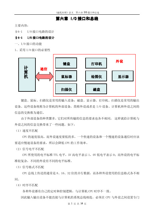
I/O接口和总线 第六章 I/O 接口和总线主要内容: §6-1 §6-1 I/O 接口电路的设计 接口电路的设计 I/O 接口电路的设计一、I/O 接口的功能 1、采用 I/O 接口的必要性键盘通信 鼠标器 绘图仪 显示器扫描仪键盘、鼠标、扫描仪是常用的输入设备;磁盘、显示器、打印机、扫描仪是常用的输出 设备。
这些设备统称为计算机的外部设备,简称外设或者是 I/O 设备。
计算机和外设之间的 信息的交换称为通信。
由于外部设备的种类繁多,它们对所传输的信息的要求也各不相同, 这样就给计算机与 外设之间的信息交换带来了一些问题,如下: (1)速度不匹配 CPU 的速度很高,而外设速度要低的多,一个快速的设备和一个慢速的设备通信时应该 要适应慢速设备的要求,所以会降低 CPU 的工作效率。
(2)信号电平不匹配 CPU 所使用的电平标准 TTL 电平,5V 高电平表示 1,0V 低电平表示 0;而外设的电平标 准较复杂,不同的外设有不同的电平标准。
(3)信号格式不匹配 CPU 总线上传送的通常是 8、16、32 位的并行数据,而各种外设使用的信息格式各不相 同。
(4)时序不匹配 各种外设都有自己的定时和控制逻辑,与计算机 CPU 时序不一致。
因此输入输出设备不能直接与计算机的系统总线相连,必须在 CPU 与外设之间设置专门1 16线总和口接外设 打印机 磁盘页章六第 义讲》理原机微《 共页 第计算机 计算机 计算机 计算机I/O接口电路。
2、接口功能 接口电路是专门为解决 CPU 与外设之间不匹配而设置的电路,它一般应具备以下基本功 能: (1)设置数据缓冲器解决速度不协调问题 经常使用锁存器和缓冲器实现此功能。
(2)设置信号电平转换电路 通过在接口电路中设置电平转换电路解决外设和 CPU 之间信号电平不一致的问题。
(3)设置信息转换逻辑以满足对各自格式的要求 将外设信息的格式转换成 CPU 可以接受的格式,如:通过 ADC 将模拟量转换成计算机可 以接受的数字量;或者通过 DAC 将计算机送出的数字量转换成模拟量去驱动外设工作。


运算放大器集成电路手册-目录:集成运算放大器参数与参数符号1第1章通用运算放大器3LH0021/0021C多片式通用功率运算放大器3LH0041/0041C多片式通用功率运算放大器8LM10/10B/10C/10BL/10CL具有电压基准的通用运算放大器12LM101A/201A/301A外补偿通用运算放大器25LM107/207/307通用运算放大器37LM108/208/308,LM108A/208A/308A超β管输入外补偿通用运算放大器43 LM124/224/324,LM124A/224A/324A四单电源通用运算放大器52LM148/248/348四通用运算放大器61LM158/258/358,CF158A/258A/358A双单电源通用运算放大器67MC1437/1537双对称通用运算放大器72MC1456/1556通用运算放大器74MC1458/1558,MC1458N/1558N双通用运算放大器78MC3303/3403/3503四通用运算放大器83MC4558/4558A/4558C双通用运算放大器87OP02/02A/02C/02D通用运算放大器92OP04/04A/04B/04C/04D/04E双对称高性能通用运算放大器98OP07/07A/07C/07D/07E超低失调高精度运算放大器104OP14/14A/14C/14D/14E双对称高性能通用运算放大器113μA709/709A/709C外补偿通用运算放大器117μA741/741A/741C/741E通用运算放大器124第2章高精度运算放大器134AD8615/16/18精度为20MHz CMOS线到线输入/输出运算放大器134ALD2724E/2724双精度高转换速率CMOS运算放大器142LMP2011/12高精度,线到线输出运算放大器146LT1013/1013A/1013D双高精度运算放大器155LT1014/1014A/1014D四高精度运算放大器167LTC1052/1052CCMOS斩波稳零高精度运算放大器176LTC7652CCMOS斩波稳零高精度运算放大器186OP17A/17B/17C/17E/17F/17G精密JFET输入运算放大器188OP27A/27B/27C/27E/27F/27G低噪声高精度运算放大器194OP42A/42E/42F高速快建立时间精密JFET输入运算放大器203OPA734/735/2734/27350 05μV/℃单电压CMOS运算放大器210TL2652/2652ACMOS斩波稳零高精度运算放大器218TL2654/2654ACMOS斩波稳零高精度运算放大器226THS4304低失真5V单电源宽带运算放大器234μA714/714C/714E高精度运算放大器250μA725/725A/725C/725E高精度运算放大器257第3章低噪声运算放大器265AD8099低噪声低失真高速运算放大器265LT1007/1007A低噪声高精度运算放大器270LT1037/1037A低噪声高精度运算放大器277OPA725/726/2725/2726非常低噪声,高速12V CMOS运算放大器281第4章高速运算放大器290AD507J/507K/507S高速宽带运算放大器290AD509J/509K/509S高速宽带运算放大器291HA2510/2512/2515高速运算放大器293HA5101高精度运算放大器297HA5111外补偿高精度运算放大器301LH0002/0002C高速电流放大器(电压跟随器)304LH0063/0063C高速宽带JEET输入电压跟随/缓冲放大器306LM6161/6261/6361高速运算放大器309LMF118/218/318外补偿高速运算放大器316LT1055/1055A/1055C精密高速JFET输入运算放大器325MC1436/1536高压运算放大器333MC1439/1539高速运算放大器335第5章宽带运算放大器340EL5160/5161/5260/5261/5360200MHz低功率电流反馈放大器340HA2541宽带高速快建立时间运算放大器345HA2600/2602/2605宽带运算放大器349LMH6628双宽带、低噪声电压反馈运算放大器354LMH6657/6658270MHz单电压,单和双放大器361LMH6682/6683190MHz单电压,双和三运算放大器375LMH67021 7G超低失真,宽带运算放大器388LMH67031 2G低失真运算放大器394LMH6723/24/25单/双四芯线组370MHz 1mA电流反馈运算放大器402LMH6738宽带,低失真三倍运算放大器413LT6230/30 10/31/32215M线到线输出1 1nV/Hz,3 5mA运算放大器419 MCP6291/2/3/4/51 0mA 10MHz线到线运算放大器437MIC92080MHz低功率SC 70运算放大器446MIC92145MHz低功率SC 70运算放大器455MIC922230MHz低功率SC 70运算放大器464MIC923410MHz低功率SC70运算放大器472OPA690宽带,电压反馈运算放大器失真480OPA691宽带,电流反馈运算放大器失真490OPA727/728/2727/4727微调20MHz,高精度CMOS运算放大器500OPA842宽带,低失真,单位增益稳定电压反馈运算放大器508OPA2614双,高增益带宽,高输出电流运算放大器517THS3001420MHz高速电流反馈放大器529TS615双宽带运算放大器与高输出电流541TS616双宽带运算放大器与高输出电流553TSH80/81/82宽带线到线运算放大器与备份功能565第6章低功耗运算放大器575CA3078A/3078微功耗运算放大器575LM13080功率程控运算放大器580ICL7611A/7611B/7611DCMOS 低功耗运算放大器585ICL7612A/7612B/7612DCMOS 低功耗运算放大器591ICL7621A/7621B/7621D双CMOS 低功耗运算放大器594LF441/441A低功耗JFET输入运算放大器597TL060/060A/060B低功耗JFET输入运算放大器602LM4250/4250C低功耗程控运算放大器606LTC2054/55单/双微功零漂移运算放大器613OP90A/90E/90F/90G精密低压微功耗运算放大器621第7章其他运算放大器629CA3130/3130AMOSFET输入运算放大器629LF155/255/355,LF155A/355A/355BJFET 输入运算放大器(低电源电流)634 LF156/256/356,LF156A/356A/356BJFET输入运算放大器(带宽)641LF157/257/357,LF157A/357A/357BJFET输入运算放大器(带宽、欠补偿)650 LH0101/0101A多片式JEET输入功率运算放大器657LM143/343高压运算放大器663LM144/344外补偿高压运算放大器672LM146/246/346四程控运算放大器677LM159/359双电流差动运算放大器685LM2900/3900四电流差动运算放大器694LM3301/3401四电流差动运算放大器706TS982线到线高输出电流与双运算放大器707。

运放型号简介1.普通运放:(1)运放LM301 运算放大器 NS[DATA]LM308 运算放大器 NS[DATA]LM308H 运算放大器(金属封装) NS[DATA]LM741 NS[DATA] 通用型运算放大器 HA17741(2)单运放TL061 BI-FET单运算放大器 TI[DATA]TL081 BI-FET单运算放大器 TI[DATA]LF351 BI-FET单运算放大器 NS[DATA]LF356 BI-FET单运算放大器 NS[DATA]LF357 BI-FET单运算放大器 NS[DATA]LF411 BI-FET单运算放大器 NS[DATA](3)双运放TL082 BI-FET双运算放大器 TI[DATA]TL072 BI-FET双运算放大器 TI[DATA]TL062 BI-FET双运算放大器 TI[DATA]LF353 BI-FET双运算放大器 NS[DATA]LF412 BI-FET双运放大器 NS[DATA]LM1458 双运算放大器 NS[DATA]LM2904 双运放大器 NS[DATA]/TI[DATA](4)四运放LM358 NS[DATA] 通用型双运算放大器 HA17358/LM358P(TI) LM324(NS[DATA]) 四运算放大器 HA17324,/LM324N(TI) LM348 四运算放大器 NS[DATA]LM148 四运算放大器 NS[DATA]LM2902 四运算放大器 NS[DATA]/TI[DATA]LM3900 四运算放大器TL064 BI-FET四运算放大器 TI[DATA]TL074 BI-FET四运算放大器 TI[DATA]TL084 BI-FET四运算放大器 TI[DATA]2.音频视频放大器:LM380 音频功率放大器 NS[DATA]LM386-1 NS[DATA] 音频放大器 NJM386D,UTC386 LM386-3 音频放大器 NS[DATA]LM386-4 音频放大器 NS[DATA]LM3886 音频大功率放大器 NS[DATA]TBA820M 小功率音频放大器 ST[DATA]MC34119 小功率音频放大器NE592 视频放大器3.高精高速低功耗运放:LM725 高精度运算放大器 NS[DATA]OP07-CP 精密运算放大器 TI[DATA]OP07-DP 精密运算放大器 TI[DATA]LM318 高速运算放大器 NS[DATA]NE5532 高速低噪声双运算放大器 TI[DATA]NE5534 高速低噪声单运算放大器 TI[DATA]LM124 低功耗四运算放大器(军用档) NS[DATA]/TI[DATA] LM224J 低功耗四运算放大器(工业档) NS[DATA]/TI[DATA]4.特色运放:LM733 带宽运算放大器CA3130 高输入阻抗运算放大器 Intersil[DATA]CA3140 高输入阻抗运算放大器CD4573 四可编程运算放大器 MC14573ICL7650 斩波稳零放大器LF347(NS[DATA]) 带宽四运算放大器 KA347LF398 采样保持放大器 NS[DATA]。

CH6数显仪说明书前言感谢您选用我公司的产品,我们相信这种数显表会达到您预期的使用目的。
在本说明书内,关于CH6数显仪系列方面的内容,将尽可能为您作明确而又详尽的说明。
为保证您的设备有效和可靠地安全运行,使用前请详细阅读和理解相关说明书,尤其是有关安全规范的章节,请务必按照本说明书关于安全操作的指引去做,并制定出本单位的安全操作规程。
如果因为违反本说明书的指引或本单位的操作规程而发生的设备或人身等安全事故,应由违章者负责。
但本公司将始终如一地愿意为用户提供完善的售后服务。
请妥善保存本说明书以便随时查阅。
本说明书的有关产品的技术参数、产品结构图样和表格是本公司独有的技术资料,不许复印,更不得向外扩散。
否则作侵权处理。
本公司有权追究违反者的侵权责任。
未经本公司同意而对本机进行结构性更改,或使用非本公司生产的不合格零配件而造成机器的损坏,本公司将考虑终止或有条件地对其实行保修或提供优惠的用户服务。
CH6系列数显仪使用说明 ver:09.111、概述CH6系列数显仪与各类模拟量输出的传感器、变送器配合,完成温度、压力、液位、成分等物理量的测量、变换、显示和控制.S,并具备调校、数字滤波功能误差小于0.5%F适用于标准电压、电流、热电阻、热电偶等信号类型2点报警输出,上限报警或下限报警方式可选择。
报警灵敏度独立设定变送输出(选装),能将测量、变换后的显示值以标准电流、电压形式输出供其它设3、技术规格3、技术规格电源:85V AC~265V AC,120VDC~380VDC,功耗小于6W12VDC~36VDC,功耗小于6W★注:直流供电电源应留有一定功率余量,请按每台24VDC/0.5A, 12VDC/2A配置电源。
并注意电源线长度和线径。
工作环境:0℃~50℃,湿度低于90%R.H,不结露。
显示范围:-1999~9999,小数点位置可设定输入信号类型:万能输入,可通过参数设定选择注:0~10VDC输入订货时注明或用户自行更改,拆开仪表机壳,将仪表主板(输入信号端子所在电路板)背面(元器件的反面)SL1间的连线割断,然后修改输入信号选择参数即可。
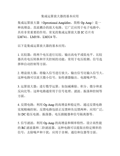
集成运算放大器的基本应用
集成运算放大器(Operational Amplifier,简称Op Amp)是一
种高增益、直流耦合的放大电路。
它广泛应用于电子电路中,具有非常重要的作用。
常见的集成运算放大器IC芯片有
LM741、LM358、LM324等。
以下是集成运算放大器的基本应用:
1. 比较器:将两个电压进行比较,输出高电平或低电平。
比较器具有电压转换和开关控制的功能,常用于电压检测、信号选择和自动控制等方面。
2. 增益放大器:将输入信号进行放大,输出信号比输入信号大。
这种电路可以放大微小信号,如传感器输出、电源噪声等。
3. 运算放大器:进行数学运算,如加减乘除、积分、微分和求反向比等。
这种电路通常用于信号处理、滤波、振荡和控制等方面。
4. 反馈电路:利用Op Amp的高增益和稳定性,通过反馈电路实现精确控制。
反馈电路包括正反馈和负反馈两种,应用广泛,如DC稳压电源、振荡器、电压跟随器和信号隔离器等。
5. 信号滤波:利用Op Amp的高增益和频率特性,设计高性能的RC滤波器和二阶滤波器。
这种电路可以提取出特定频率的
信号,去除噪声和干扰,应用于音频、通信和仪器等方面。
总之,集成运算放大器广泛应用于各种电子电路中,可以实现信号放大、滤波、比较和控制等多种功能,是电子工程师必不可少的工具。
