来自ST的MEMS麦克风使用指南,含参数计算
- 格式:pdf
- 大小:952.26 KB
- 文档页数:20

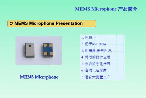

MEMS 麦克MMIC 系列特点(SMT)260 °C指令对应,Ni/Au 镀金终端适合无铅焊锡。
用途PDA,笔记本电脑,照相机等的麦克应用指南:智能手机/平板终端型号的命名方法产品阵容MMIC271609T4064C0300系列名称L×W×H 尺寸型名包装数量(个)(mm)271609 2.7×1.6×0.89C03003,000332509 3.35×2.5×0.98C09009,000MMICT4076-00-908系列名称型名版本一个卷轴的数量卷带宽度T4076909,00088mmT4078型号L×W×H 尺寸(mm)Nom.灵敏度/(dBV/Pa)信噪比(Nom.)/dB(A)声压级/dB产品类型端口位置使用温度范围/°C 单个重量/gMMIC271609T4064C03002.7×1.6×0.89–38±3 at 1kHz 61.5110at THD 1% Max.,1kHz模拟输出(不平衡)底部–40 to 850.016MMIC332509T4081C09003.35×2.5×0.95–38±1 at 1kHz 66136at THD 10% Typ.,1kHz模拟输出(平衡)底部–40 to 850.019MMICT4076-00-9082.75×1.85×0.9–38+/-1 at 1kHz 63127at THD 10% Max., 1kHz模拟输出(不平衡)底部0 to 850.02MMICT4078-00-9083.35×2.5×0.98–38±1 at 1kHz 66135at THD 10% Max, 1kHz模拟输出(平衡)底部–40 to +850.019MMIC271609T4064C0300(模拟输出(不平衡))形状与尺寸推荐焊盘布局端口位置: 底部电气特性其他灵敏度–38dBV/Pa ±3dBV/Pa at 1kHz 信噪比 (SNR) (T yp.)61.5 dB(A)总谐波失真 (THD) (Max.)1% at 110 dB SPL, 1kHz电源电压抑制比 (PSPR) (T yp.)75dB at 1kHz sine wave, 100mVp-p 消耗电流 (Icc) (T yp.)90µA 输出阻抗 (Max.)400使用温度范围–40 to 85°C包装形式载带编带(180mm 卷筒、编带宽度 8mm)包装数量3000pcs 重量0.016gMMIC332509T4081C0900(模拟输出(平衡))形状与尺寸推荐焊盘布局端口位置: 底部电气特性其他灵敏度–38dBV/Pa ±1dBV/Pa at 1kHz 信噪比 (SNR) (T yp.)66dB(A)总谐波失真 (THD) (T yp.)10% at 136 dB SPL,1kHz电源电压抑制比 (PSPR) (T yp.)70 dB at 1kHz sine wave, 200mVp-p 消耗电流 (Icc) (T yp.)135µA 输出阻抗 (OUTP to OUTN) (Typ.)450Ω输出阻抗 (OUTP as co u pled to GND) (T yp.)225Ω输出阻抗 (OUTN as co u pled to GND) (Typ.)225Ω使用温度范围–40 to 85°C包装形式载带编带(330mm 卷筒、编带宽度 8mm)包装数量9,000pcs 重量0.019g形状与尺寸推荐焊盘布局端口位置: 底部电气特性其他灵敏度–38dBV/Pa +/-1dBV/Pa, at 1kHz SN63dB(A)THD (T yp.)10% at 127dB SPL, 1kHz PSRR (T yp.)75dB at 1kHz, 200mVp-p 消耗电流 (T yp.)135µA 输出Z (T yp.)250使用温度范围0 to 85°C包装形式载带编带(330mm 卷筒、编带宽度 8mm)包装数量9,000个重量0.02g形状与尺寸推荐焊盘布局端口位置: 底部电气特性其他灵敏度–38dBV/Pa ±1dBV/Pa at 1kHz SN66dB(A)THD (T yp.)10% at 135dB SPL, 1kHzPSRR (T yp.)90dB at 1kHz sine wave, 200mVp-p 消耗电流 (T yp.)250µA 输出Z (T yp.)250使用温度范围–40 to 85°C包装形式载带编带(330mm 卷筒、编带宽度 8mm)包装数量9,000个重量0.019gMMIC 系列推荐回流焊温度曲线图Note : Specified at solder pads包装形式数值为typ.值。
SPECIFICATION OF DIGITAL MEMS MICROPHONEDIRECTIVITY : OMNI-DIRECTIONAL SOUND PORT : TOP PORT TYPE DATE : 2013. 07. 12H FBFRs/CFRs/PVC -Free※ Halogen FreeMODEL NO. : F1-(W)CDMO-D100T26-5PBSE CO., LTD58B-4L, 626-3, GOZAN-DONG, NAMDONG-KU INCHON-SI. KOREA TEL :(8232) 550-1780 FAX :(8232) 554-62064 05 8 1 7-USERPrepared Checked Checked ApprovedName SignBSEPreparedCheckedCheckedApprovedNameY .H.Shim S.H.Lee M.J.LeeSignSPECIFICATION HISTORY Version Date Comments1.0 July, 12, 13 1st Submission of Electro-Acoustical specification1. INTRODUCTIONThis specification is for the SMD possible Digital MEMS (Top port) Microphone which has endurable reflow temperature of up to 260℃ for over 15 seconds. The output of microphone is a digital serial bit stream.2. MODEL NO.F1-(W)CDMO-D100T26-5P3. ELECTRO-ACOUSTIC CHARACTERISTICSParameterConditionsMinTyp MaxUnitsDirectivity Omni-directionalSupply Voltage 1.64 - 3.6 V Sensitivityf=1kHz, 1Pa(94dBSPL)-29 -26 -23 dBFS Signal to Noise Ratiof=1kHz, A-Weighted, Clk f=2.4㎒ -59-dB(A)Digital Noise Floor Integrated, f=20Hz to 20kHz, A-Weighted - -85 - dBFSCurrent consumption Normal operation350 - 450 uA Standby Current--10uAPSRMeasured with 217Hz square wave and broad band noise, both 100mVpp- - - 78 dBFSTotal Harmonic Distortion + Noise100dB SPL, at 50Hz ~ 4kHz- - 1 %115dB SPL, at 1kHz - - 5 120dB SPL, at 200Hz- - 10 Maximum Input Signal THD<10%, at 1kHz120 - - dBSPL Short circuit current1-10mA Temp. = 23 ± 2 ℃Room Humidity = 65 ± 5 %TEST CONDITION : Vdd = 1.8V, Clock Frequency = 2.4MHz4. MEASUREMENT CIRCUIT5. PIN DESCRIPTIONPin Name DescriptionVDD Supply and IO voltage for the microphoneL/R_Select Left/Right ( DATA2 / DATA1) channel selectionCLOCK Clock input to the microphoneDATA PDM data output from the microphoneGND Ground6. INTERFACE PARAMETERSParameter Symbol Min Typ Max Unit Clock freq. ( sample rate ) f CLK 1 3.25 MHz Clock duty cycle f DC40 50 60 % Power supply V DD 1.64 1.8 3.6 V Input/Output voltage low V IOL-0.3 0.35*V DD V Input/Output voltage high V IOH0.65*V DD V DD+ 0.3 V7. SLEEP MODEThe sleep mode is entered by stopping the clock or lowering the clock frequency below stand-by clock frequency.Parameter Symbol Min Typ Max Unit Wake-up time t UP10 ms Fall-asleep time t DOWN10 ms Standby current I SB10 ㎂Standby clock frequency f CLKSB 1 ㎑8. INTERFACE TIMING CHARTParameter Symbol Min Typ Max Unit Clock rise time t CR10 ns Clock fall time t CF10 ns Delay time for data valid t DV31 77 ns Delay time for data high Z t DH8 15 ns9. CHANNEL DATA CONFIGURATIONData symbol inData asserted at Data sampled at L/R Select connected to interface timing chartDATA1 Falling clk edge Rising clk edge GNDDATA2 Rising clk edge Falling clk edge V DDor GND on the phone PWB※ Stereo operation is accomplished by connecting the L/R_Sel pin either to VDD10. ENVIRONMENTAL CHARACTERISTICS AND STANDARD CONDITIONSItem Min Typ Max Unit Operating temperature range -30 +70 ℃Storage temperature range -40 +85 ℃Relative humidity 25 85 %Air Pressure 860 1060 mBar Standard temperature range 15 20 25 ℃Standard Relative humidity 40 60 %F1-(W)CDMO-D100T26-5PFar Field Measurement Condition Temperature : 23 ± 2 ℃ Supply Voltage : 2.0VAcoustic stimulus : 1Pa ( 94㏈ SPL at 1㎑ ) at 50 ㎝ from the loud-speaker.The loud-speaker must be calibrated to make a flat frequency response input signal. Position : The frequency response of microphone unit measured at 50㎝ from the loud-speaker12. MECHANICAL CHARACTERISTICS※ PCB design & Pin size can be changed by model No.SMD Type11. TYPICAL FREQUENCY RESPONSE CURVE4.00±0.13.00±0.11.00±0.1Dimensions (Unit : mm)Item Dimension Tolerance (+/-) Units Length (L) 4.00 0.10 mm Width (W) 3.00 0.10 mm Height (H) 1.00 0.10 mm Acoustic Port (AP) Φ 0.650.10 mmPin # Pin Name Type Description1 CLK Clock Clock input2 DATA Data PDM data output3 VDD Power Supply and I/O voltage4 L/R L/R Select Left/Right channel selection5 GND Ground GroundRecommendedPCB land pattern(Unit : mm)Recommendedsolder stencil pattern(Unit : mm)( thickness of metal mask: 0.10T)- Reel•13” reel for the mass production stage.(Unit : mm)- TapingPin 4Sound Hole [ Note ]1. Direction of parts : See above pictures.2. Microphone total quantity (13” Reel) : 4,000pcs3. ESD : 102~1012Ω4. Cover Tape Material & Color : PS, BlackUnit : mm A0 4.30±0.10 E 1.75±0.10B0 3.20±0.10 F 5.50±0.05K0 1.30±0.10 T 0.30±0.05D0 1.50±0.10 W 12.00±0.3013. Packaging Specification - PackingInner Box spec.Outer Box Spec. 1 Inner Box included 2 reels→ Microphone total quantity : 8,000 pcs 1 Outer Box included 5 Inner Boxes→ Microphone total quantity : 40,000 pcs14. RELIABILITY TEST CONDITIONSNote : After test conditions are performed, the sensitivity of the microphone shall not deviate more than ±3dB from its initial value.TEST DESCRIPTIONTEMPERATURE STORAGE [High Temperature Storage]+70±2℃ environment for 200 hours.(The measurement to be done after 2 hours of conditioning at room temperature) [Low Temperature Storage]-25±2℃ environment for 200 hours.(The measurement to be done after 2 hours of conditioning at room temperature)HUMIDITY +70±2℃ and 95±2%RH environment for 200 hours.(The measurement to be done after 2 hours of conditioning at room temperature)TEMPERATURECYCLE 5 cycles of temperature change.+70±2℃ for 1hr, at 20±2℃ for 30 min, at -25±2℃ for 1hr(The measurement to be done after 2 hours of conditioning at room temperature)THERMAL SHOCK 32 cycles of temperature change.from –40℃ to 85℃ for 1hr Changing time about 5 min(The measurement to be done after 2 hours of conditioning at room temperature)HIGH TEMPERATURE AND HUMIDITY +85±2℃ and 85±2%RH environment for 120 hours.(The measurement to be done after 2 hours of conditioning at room temperature)ESD (Electrostatic Discharge) HBM (Human Body Model) : 2kV Expose 10 Times.MM (Machine Model) : 0.2kV Expose 10 Times.CDM (Charged Device Model) : 0.5kV Expose 10 Times.VIBRATION To be no interference in operation after vibrations.10㎐ to 55㎐ for 1 minute full amplitude 1.52㎜ , for 2 hours at three axesDROP To be no interference in operation after dropped to steel floor 12 times from 1.5 meter height in state of packingREFLOWSENSITIVITY3 reflow cycles. Refer to reflow profile from specification item 11.15 . TEMPERATURE CONDITIONS15.1 STORAGE TEMPERATURE : -40℃ ~ +100℃15.2 OPERATING TEMPERATURE : -40℃ ~ +100℃16. MEASUREMENT SYSTEM4231 Sound CalibratorPrinterTested mic.ComputerTurn-Table ControllerRef. Mic50㎝Loud-speaker (SPL : 1Pa)Audio Analyzer Type 2722Power Amplifier Type 2718Turn-TableAnechoic ChamberDecimation BoardAmplifiers Types 2690MachineModel NoPurposeStandard MIC 4191 Revision of input signal & SPK spec Audio Precision AP2722 Audio Analysis Evaluation Board ADAU1301EB Signal TransformationLoud-speaker GRF Memory HESPK (Input sound Signal occur) Power Amplifier2718 Power amplificationCharging Conditioning Amplifier 2692Ref. MIC Signal Transformation Operating Software A-D Freq. Resp.Sound Level Calibrator4231 Standard MIC Calibration purpose16.1 Measurement Condition(a) Supply voltage : 1.8V (b) Clock Frequency : 2.4 ㎒(c) Acoustic stimulus : 94㏈ SPL at 1㎑ (d) Distance between MIC & SPK : 50㎝(e) Measurement frequency : 80 (㎐) ∼ 16 (㎑)170~180℃Pre-heat 120 sec 230℃260℃Solder melt 100 secStageTemperature ProfileTime (maximum)Pre-heat 170~180 ℃ 120 sec Solder MeltAbove 230 ℃ 100 sec Peak260 ℃ maximum30 sec[Notes]1. Do not pull a vacuum over the port hole of the microphone. Pulling a vacuum over the port hole can damage the device.2. Do not board wash after the reflow process. Board washing and cleaning agents can damage the device. Do not expose to ultrasonic processing or cleaning.3. Recommend no more than 3 cycles.4. Shelf life : Twelve(12) months when devices are to be stored in factory supplied, unopened ESD moisture sensitive bag under maximum environmental condition of 30℃, 70% R.H.5. Exposure : Devices should not be exposed to high humidity, high temperature environment. MSL (Moisture sensitivity level) Class 2a.6. Out of bag : Maximum of 90 days of ESD moisture sensitive bag, assuming maximum conditions of 30℃, 70% R.H.17. SOLDER REFLOW PROFILE18. Recommended Pick-up nozzle18.1. Nozzle material : Metal or Rubber, Etc.18.2. Case Weight- If tool outer size is bigger than MIC. : Max. 10N- If tool outer size is smaller than MIC. : Max. 4N18.3. Nozzle position : The opposite side of sound hole- Nozzle inner diameter size : Max. Ø1.1- position : 0.90mm away from the MIC center19.1. Handling Guide of Cleaning & Foreign Matter* Note 1. No Liquid or/and gas should be used for washing / cleaning.* Note 2. No board washes should be applied after reflow* Note 3. No foreign matter should be exposed interior microphone during cleaning or washing.if cleaning or washing is applied unavoidably, It must do additional prevention in area of “Microphone sound hole” to avoid foreign matter.(ex. Attached protective tape) * Note 4. No seal sound hole of microphone should be applied during reflow process* Note 5. No ultrasonic cleaning should be applied in case of microphone unit itself or/and after installed microphone onto board.* Note 6. Do no reuse microphone which is defect during SMD.Do no wash or clean to reuse microphone which is defect during SMD.De-cap View ofGood part► Example) De-cap View of the NG MicrophoneReflow after sealing of Sound Hole Defect view NG MIC by Pick-up Defect view NG MIC by ultrasonic cleaning Defect view NG MIC by liquid foreign matter19.2. Handling Guide of Care of Board Routing & Cutting* Note 1. Do work maximum distance with microphone and minimum speed machining setting during Board Routing & Cutting* Note 2. Do not wash or clean “Board” after Board Routing & Cutting* Note 3. Do additional prevention in area of “microphone sound hole” to avoid foreignmatter(ex. Attached protective tape) during Board Routing & Cutting* Note 4. Do not use strong air flow directly in order to remove foreign matter should be applied in microphone* Note 5. Do preventive action in area of “microphone sound hole” to avoid foreignmatter(ex. Attached protective tape) or air .(ex. Block “Microphone sound hole” by hands as below picture)► Example) Air Blowing ConditionN.GExample) Do block “Microphone Sound Hole”by hands during air blow19.3. Inspection by X-Ray* Note 1. Do inspect X-Ray after SMD.It is different X-Ray condition by applied SMD company.20.1. Recommended Heater Gun SpecificationManufacturer HAKKO Model 850B ESD Temperature control 100 ~ 420 Top heaterType Hot air flowFlow rate < 23 ℓ/min Alignment visualPick-up ManualSolder/flux 1. Removing or pre-heating the solder residue before mounting new part2. Apply lead-free flux only or apply 2 ~ 3 points of solder paste instead1.5cm Heater gun nozzle MICPCB15.2. Recommended Heater Gun Setting ConditionHeater gun setting Temperature 300 ℃ ~ 400 ℃Nozzle & MIC. Length 1.5 cmFlow setting 2.0 ~Alignment VisualPick-up ManualWorking TimeRemove 10 ~ 20 secSMD 10 ~ 20 sec * Note 2. According to Rework M/C & Worker, this condition will be change.* Note 1. According to the material & thickness & counts of layer for PCB, this condition will be change.Bottom Heater Recommend IR heater.Alignment Use magnifier for alignment.Note : it may difficult to do alignment by naked visual because MIC pad is located on soffit.Temperature Recommend temperature is “300℃”.Time It is the optimized working process of 1.0 ~ 2.0mm board for 10~20sec under 300℃ temp.Nozzle Use heater gun without nozzleSolder/flux Process Options 1. Removing the solder residue before mounting new part- print Halogen-free solder paste on the SMD MICterminals using mask mounting2-1. Pre-heating the solder residue before mounting new part - apply Halogen-free flux onto the land pattern2-2. Pre-heating the solder residue before mounting new part - apply 2 ~ 3 points of Halogen-free solder paste onto theland pattern3. Highly recommendation process for rework.- After remove defect parts without Pre-heating,It is used Halogen-free flux or 2~3 points of Halogen-free solder. (It is most effective and fast for rework)20.3. Rework Process Condition (using Heater Gun)Microphone Technology Leadership * Note 1. Follow standard guide line of SMD company for Rework Condition* Note 2. Rework conditions may variable by SMD companies' circumstance and working condition.* Note 3. Do Not reuse defect microphone by SMD process.* Note 4. Do not employ chemical board wash or cleaning, as the associated cleaning agents (such as liquid or air) can damage the device.20.4. Handling of Rework21 20. REWORK。
mems mic内部阻抗
MemS Mic(微机电系统麦克风)是一种基于微机电系统技术
制造的麦克风,其内部阻抗取决于其设计和制造过程中使用的材料和结构。
一般来说,MemS Mic的内部阻抗相对较低,一
般在几百到几千欧姆之间。
MemS Mic的内部阻抗会对其电路特性和性能产生一定影响。
较低的内部阻抗可以提供较低的噪声和失真水平,对于麦克风的声音捕捉和放大能力有着积极影响。
此外,较低的内部阻抗也使得麦克风能够更好地适配信号处理电路,并提供更好的频率响应和动态范围。
然而,不同型号和品牌的MemS Mic可能具有不同的内部阻抗。
因此,在使用时,应该注意按照具体的产品规格和设计要求来选择适当的MemS Mic,并注意其内部阻抗的要求和特性。
WX-ST200 Wireless Handheld Microphone Part of Panasonic's SR200P 1.9 GHz Digital WirelessMicrophone system, the WX-ST200handheldmicrophone is the perfect solution for education and/or corporate presentations. This condenser microphone is optimized for vocal clarity with Panasonic's proprietary filtering to eliminate noise yet provide clear and original sound quality with a flat frequency response. Engineered to withstand the classroom environment, the WX-ST200 is lightweight yet durable. At just 0.4lbs. (with onestandard or rechargeable AA battery inserted), thishandheld microphone is one of the lightest handheldmicrophones on the market, so the end user can focus onthe message they want to deliver during a class,conference, or all-day training. The microphone alsofeatures a 3.5mm audio input connector, so the end usercan easily use the same system to transmit audio from alocal source such as a laptop. Ships with 4 octogen colorrings for easy personalization.Contactless desktop charger (WX-SZ200) soldseparately.•Crystal Clear Sound, Optimized for VocalPresentations•Easy Setup, with automatic channel assignmentthanks to DECT 1.9 GHz wireless technology•Lightweight (0.4 lbs. with battery included)•Rugged and Durable•Only one AA battery required (alkaline orrechargeable)•Easy & Convenience to usePanasonic WX-ST200 Features & Specifications Page 1 of 2Panasonic WX-ST200 Features & SpecificationsPage 2 of 2 Microphone Element: Electret CondenserMicrophone Polar Pattern:Cardioid Frequency Response: 100 Hz to 15 kHzWireless Frequency:1920 MHz to 1930 MHz Operating Ambient Temp.:41° F to 95° F (5° C to 35°C) LED Indicators:Power, Charge Battery Required:Rechargeable: 1 x AA Ni-MH Dry cell: 1 x AA alkalineBattery Life:NI-MH: Approx. 8 hours Alkaline: approx. 6 hoursWarranty (Parts & Labor):3 yearsDimensions (Max Diameter x L):1-57/64 x 8-47/64 inches (48mm x 222mm)Weight (including battery):0.4 lbs. (180 g)Leveraging Panasonic's20-year experience in DECT wireless audio communications, the WX-SR200P 1.9 GHz digital wireless microphone system is the best-in-class solution for classroom or corporate presentations providing low latency for hybrid in-room/virtual presentations. Panasonic's digital wireless microphone system is easy to set up, easy to integrate with third-party control systems (such as Crestron and Extron) and easy to use. Setup is a breeze - the WX-ST200 pairs wirelessly with Panasonic's WX-SR202 receiver and assigns channels automatically, eliminating the need for manual channel assignment. The system can be expandable to suit a variety of spaces, from small classrooms, medium sized classrooms / conference rooms, to largeauditoriums. Up to 8 separate antennas (per receiver) can bemounted to the wall or the ceiling in the room and connected viaCAT5 back to the receiver locked away in a cabinet or closet andmultiple 2-channel receivers can be installed to add wirelessmicrophone channels to the room.。
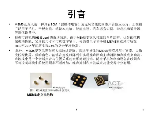
提升MEMS麦克风灵敏度的设计方法■周建民[摘要]微机电系统(MEMS)麦克风性能可望大幅提升。
传统顶部收音麦克风的后室空气容积较小,使得信噪比(SNR)表现受到局限,因此半导体厂家利用创新封装技术,将后共振腔室扩大,以降低杂音,达到更出色的灵敏度。
[关键词]微机电系统MEMS麦克风共振腔[中图TN64 [文献标识码]A [文章编号]1674-2583(2014)11-0030-051引言微机电系统(MEMS)麦克风性能可望大幅提升。
传统顶部收音麦克风的后室空气容积较小,使得信噪比(SNR)表现受到局限,因此半导体厂家利用创新封装技术,将后共振腔室扩大,以降低杂音,达到更出色的灵敏度。
微机电系统(MEMS)技术的问世和应用,让麦克风变得越来越小、性能越来越高。
MEMS麦克风具有诸多优势,例如高信噪比(SNR)、低功耗、高灵敏度;其所用的微型封装可相容贴装工艺,且温度特性非常出色,不会受到回流焊工艺的影响。
2 MEMS麦克风及其特性2.1声学传感采用半导体工艺MEMS麦克风所用的声学传感器是利用半导体生产线制作,且通过高度自动化过程封装的晶片(图l)o MEMS麦克风的制造过程,首先是在晶圆上沉积数层不同物质,然后蚀去无用物质,在基础晶片上形成一个腔室,接着在腔室上覆盖一层能够运动的振膜,和一个固定的背板;传感器背板具有优良图1 MEMS麦克风传感器截面图的刚性,采用通孔结构,通风性能优异,当空气流过时,背板保持静止;而振膜是一个很薄的实心结构,当声波引起气压变化时,振膜将会弯曲;振膜运动时,振膜与背板间的电容量将会变化。
2. 2数字麦克风具较高抗噪性在MEMS麦克风内,特定应用集成电路(ASIC)晶片利用电荷泵在麦克风振膜上放置一个固定的参考电荷,当振膜运动导致振膜与背板间的电容量发生变化时,ASIC可测量电压变化,并将这种电容变化转换成电信号(图2)。
模拟MEMS麦克风的输出电压与瞬间气压成正比。
MEMS MIC噪声(SNR)测量的A计权算法:计算公式如下
n
L A = 10log
i
Ri:倍频程声压
△ i: 修正值
三:其他算法计算
i=23(8KHz)
L A10log[ 100i]
i = 1(63Hz)
L
A=频程声级合成后的声压级
L i 各频率声级的声压级(A计权后)
四:从已测声压级换算到 A 计权声压级
如果已知噪声的各倍频带声压级,可以将其转换为计权声压级。
如设
则按声压级定义,有
1010 P o
那么,几个倍频带声压级叠加后总声压级
L
P 为:
-n
L p
1
L =
1
- p
ioig
lz 1 10 10
1
1
[1
i =1
由总声压级L p 转换为总A 声级L P A 时,
有:
-n
L pi k i -
L
P A
=ioig
z 10
10
(dB(A))
u
式中K 为第i 个倍频带的A 计权修正值。
一般测量倍频带取 L pi 为测得的各倍频带的声压级(dB ),
L p 厂 20lg
P i
(dB )
P o (
63Hz~8kHz 的八个倍频程。
A 计权的k i 值见表1。
mems麦克风幅频曲线公式
摘要:
一、MEMS麦克风简介
1.1 微电子机械系统技术
1.2 MEMS麦克风的优点
1.3 应用领域
二、MEMS麦克风幅频曲线
2.1 定义与重要性
2.2 公式说明
2.3 参数含义
三、MEMS麦克风幅频曲线的应用
3.1 频率响应特性分析
3.2 性能优化
3.3 指导设计和制造
正文:
MEMS麦克风是一种基于微电子机械系统技术制造的麦克风,具有体积小、重量轻、功耗低等特点,广泛应用于各种语音识别、音频处理等领域。
MEMS麦克风的幅频曲线是衡量其性能的重要指标,通过计算和分析幅频曲线,可以了解麦克风的频率响应特性。
MEMS麦克风的幅频曲线公式如下:A(f) = 1 / (1 + (f - f0) / fc)
其中,A(f)表示幅频曲线,f表示频率,f0表示麦克风的谐振频率,fc表
示麦克风的截止频率。
MEMS麦克风幅频曲线的定义与重要性体现在它反映了麦克风在不同频率下的灵敏度变化。
在音频处理领域,幅频曲线可以帮助工程师设计出性能优良的音频系统,同时也可以指导麦克风的设计和制造。
在实际应用中,通过对MEMS麦克风幅频曲线的分析,可以得到麦克风的频率响应特性。
例如,在语音识别领域,麦克风的幅频曲线可以用来判断麦克风在接收语音信号时的灵敏度,进而提高语音识别的准确率。
同时,通过调整幅频曲线的形状,可以实现对麦克风性能的优化,以满足不同应用场景的需求。
总之,MEMS麦克风幅频曲线在麦克风性能分析、优化和设计制造过程中起着关键作用。
February 2017DocID025704 Rev 2 1/20 AN4426 Application note Tutorial for MEMS microphonesIntroductionThis application note serves as a tutorial for MEMS microphones, providing general characteristics of these devices, both acoustic and mechanical, as well as summarizing the portfolio available from ST. MEMS microphones target all audio applications where small size, high sound quality, reliability and affordability are key requirements.ST's MEMS microphones are designed, developed and manufactured within ST, creating an industry-unique, vertically integrated supply chain. Both analog and digital-input, top and bottom-port solutions are available.Our best-in-class AOP and SNR make ST’s MEMS microphones suitable for applications that require a very high dynamic range, improving the audio experience in any environment. Matching very tightsensitivity allows optimizing beamforming and noise cancelling algorithms for multi-microphone arrays. Low power consumption allows extending battery life.Contents AN4426 Contents1Mechanical specifications, construction details (4)2Acoustic parameters (11)2.1Sensitivity (11)2.2Directionality (11)2.3SNR (12)2.4Dynamic range and acoustic overload point (12)2.5Equivalent input noise (13)2.6Frequency response (15)2.7Total harmonic distortion (16)2.8PSRR and PSR (16)3MEMS microphone portfolio (17)4Revision history (19)2/20 DocID025704 Rev 2AN4426 List of figures List of figuresFigure 1: MEMS microphone inside package (4)Figure 2: MEMS transducer mechanical specifications (4)Figure 3: Capacitance change principle (5)Figure 4: 4 x 5 package (5)Figure 5: 3 x 4 metal cap package - bottom port (6)Figure 6: 3 x 4 package - top port (6)Figure 7: 2 x 3 package - bottom port (7)Figure 8: Faraday cage in ST’s MEMS microphones (7)Figure 9: RF immunity simulation (8)Figure 10: EMC test setup (8)Figure 11: RF test disturbance signal with sinusoidal pattern (9)Figure 12: RF immunity test results - MP34DT04 (9)Figure 13: RF test disturbance signal @ 217 Hz burst pattern (10)Figure 14: RF immunity of analog differential microphones (10)Figure 15: Omnidirectional microphone (11)Figure 16: A-weighted filter response (12)Figure 17: Acoustic and electrical relationship - analog (13)Figure 18: Acoustic and electrical relationship - digital (14)Figure 19: MP45DT02-M frequency response (15)Figure 20: MEMS microphone portfolio (17)Figure 21: MEMS microphone notation (17)DocID025704 Rev 2 3/201 Mechanical specifications, construction detailsA microphone is a dual-die device consisting of two components, the integrated circuit andthe sensor, which are housed in a package using techniques that are proprietary to ST.ASICintegratedThe sensor uses MEMS technology (Micro-Electrical-Mechanical Systems) and it isbasically a silicon capacitor. The capacitor consists of two silicon plates/surfaces. Oneplate is fixed while the other one is movable (respectively, the green plate and the grey oneshown in the following figure). The fixed surface is covered by an electrode to make itconductive and is full of acoustic holes which allow sound to pass through. The movableplate is able to move since it is bonded at only one side of its structure. A ventilation hole,allows the air compressed in the back chamber to flow out and consequently allows themembrane to move back. The chamber allows the membrane to move inside but also, incombination with the chamber created by the package will affect the acoustic performanceof the microphones in terms of frequency response and SNR.Figure 2: MEMS transducer mechanical specificationsSo basically the microphone MEMS sensor is a variable capacitor where the transductionprinciple is the coupled capacitance change between a fixed plate (back plate) and amovable plate (membrane) caused by the incoming wave of the sound.4/20 DocID025704 Rev 2Figure 3: Capacitance change principleThe integrated circuit converts the change of the polarized MEMS capacitance into a digital (PDM modulated) or analog output according to the microphone type. Finally the MEMS microphone is housed in a package with the sound inlet placed in the top or in the bottom part of the package, hence the top-port or bottom-port nomenclature of the package. ST manufactures microphones using industry-wide techniques, but also has developed innovative packaging to achieve improved performance of the microphones. Packaging techniques will be discussed in further detail.The 4x5 package is widely used to house the digital microphone MP45DT02-M. It is a common packaging technique in a top-port configuration where the ASIC is placed under the sound inlet with glue on top (glob top) in order to protect the circuit from light and the MEMS sensor is placed beside the integrated circuit. The two silicon components are fixed to the substrate and the pads of the device are on the bottom side. The resonant chambers are identified depending on the position of each chamber with respect to the membrane and the incoming sound. In this case, considering the incoming direction of the sound, the front chamber is created by the package and the chamber inside the MEMS, behind the MEMS membrane, is the back chamber. This configuration allows protecting the MEMS from dust and particles falling into the package but results in a low SNR and frequency response with a peak in the audio band.Figure 4: 4 x 5 packageThe 3x4 package is used in ST to produce both the bottom and the top-port digital microphones, MP34DB02 and MP34DT01-M, MP34DT04/-C1, and MP34DT05. Considering the bottom configuration first, this structure is depicted in the following figure. The ASIC and the MEMS sensor are fixed to the substrate and the pads of the device are on bottom side as well. The sound inlet is obtained by drilling the substrate according to the position of the MEMS sensor. The package encloses all the components. In this configuration the front chamber is the cavity of the MEMS sensor and the package creates the back chamber. This design optimizes the acoustic performance of the microphone in terms of SNR and also allows obtaining a flat response across the entire audio band. The drawback of this solution is represented by the assembly of this microphone. Usually theDocID025704 Rev 2 5/20bottom-port microphones are soldered on the PCB. The thickness of the board modifies thevolume of the front chamber, degrading the flat response of this type of microphone (referto AN4427, “Gasket design for optimal acoustic performance in MEMS microphones” fordetails). In order to minimize the artifacts caused by this environment, a flex cable isrecommended to be used. Additionally, the bottom-port microphones have a ringed metalpad around the hole. A very careful soldering process is required to avoid dust or solderingpaste from entering in the sound port, damaging the MEMS membrane.Figure 5: 3 x 4 metal cap package - bottom portThe 3x4 top-port configuration is basically a mirrored bottom-port microphone. The ASICand the sensor are placed close to each other, the sensor is still under the sound inlet butthese two components are attached to the top of the structure, in other words, the ASICand MEMS are fixed to the package lid, not to the substrate. The pads are on the substrateand thus on the bottom side of the microphone. This configuration, covered by ST patents,allows optimizing all the benefits of the bottom-port microphone in terms of acousticperformance (i.e. maximized SNR and flat band) and all the benefits related to the top-portconfiguration during the assembly process.Figure 6: 3 x 4 package - top port6/20 DocID025704 Rev 2A smaller package, 2.5 x 3.35 mm, has been introduced in ST's product portfolio (for simplicity referred to as 2x3, see Figure 7: "2 x 3 package - bottom port"). This package is a bottom-port configuration with the same internal construction as the 3 x 4 bottom-port package and it is used for the analog differential microphones MP23AB01DM/DH and analog single-ended microphone MP23AB02B. As a result of the 2x3 bottom-port package and differential output configuration, the MP23AB01DH is the best microphone provided by ST in terms of SNR and AOP.Figure 7: 2 x 3 package - bottom portMEMS microphones housed in a plastic package are protected from radiated disturbances by embedding in the plastic package a metal shield which serves as a Faraday cage. The model in the following figure shows how the Faraday cage is implemented in ST’s plastic packages.Figure 8: Faraday cage in ST’s MEMS microphonesThe next figure shows the simulation of an electric field in open space. By applying an electric field source outside the microphone package, the Faraday cage is able to considerably attenuate the field inside the microphone structure. The temperature grade of the E field is an easy way to plot the results.DocID025704 Rev 2 7/20Figure 9: RF immunity simulationIn addition to the simulation, ST has a dedicated test to evaluate immunity, “Microphonedurability to EMC disturbances”.Microphones are subjected to RF disturbances using a proper jig with the following setup.Basically the test consists of placing the microphone under an antenna radiating adisturbance signal of 1 kHz AM modulated in the range [0.8, 3] GHz. The RF amplitudediffers depending on the frequency range according to the following criteria:•+33 dBm in the range [0.8, 2.4]•+17 dBm in the range [2.4, 3.0]8/20 DocID025704 Rev 2Figure 11: RF test disturbance signal with sinusoidal patternThe carrier of the disturbance is 1 kHz since it is an audio signal. Hence, the RF immunity of the microphone is evaluated by measuring the residual of the carrier at the output of the microphone. The next figure shows the result of the peak at 1 kHz measured when applying the RF disturbance on top of an MP34DT04.In parallel with the sinusoidal pattern, another 217 Hz burst pattern used to test the RF immunity is shown in the following figure.•The RF amplitude (power): +33 dBm•Carrier frequency: 700 MHz ~ 2.5 GHz•GSM burst frequency: 217 Hz pattern (see below)DocID025704 Rev 2 9/20Figure 13: RF test disturbance signal @ 217 Hz burst patternFigure 14: RF immunity of analog differential microphones10/20 DocID025704 Rev 2AN4426Acoustic parametersDocID025704 Rev 211/202Acoustic parameters2.1SensitivityThe sensitivity is the electrical signal at the microphone output to a given acoustic pressure as input. The reference of acoustic pressure is 1 Pa or 94 dBSPL @ 1 kHz. The sound pressure level, expressed in decibel, dBSPL=20*Log(P/Po) where Po = 20 µPa is the threshold of hearing. 20*Log(1Pa/20µPa) = 94 dBSPL • For analog microphones the sensitivity is expressed in mV RMS /Pa or dBV/Pa •For digital microphones the sensitivity is expressed in dBFSdBV ≠ dBFS. It is not correct to compare different units. As given in the above equations, dBV is in reference to 1V RMS instead of dBFS where the reference is the digital full scale.2.2 DirectionalityThe directionality indicates the variation of the sensitivity response with respect to thedirection of the arrival of the sound. MEMS microphones from ST are omnidirectional which means that there is no sensitivity change to every different position of the source of thesound in space. The directionality can be indicated in a Cartesian axis as sensitivity drift vs. angle or in a polar diagram showing the sensitivity pattern response in space.The following figure depicts the directionality in these two reference systems.Figure 15: Omnidirectional microphoneAcoustic parametersAN442612/20DocID025704 Rev 22.3 SNRThe signal-to-noise ratio specifies the ratio between a given reference signal to the amount of residual noise at the microphone output. The reference signal is the standard signal at the microphone output when the sound pressure is 1Pa @ 1 kHz (microphone sensitivity). The noise signal (residual noise) is the microphone electrical output at silence.This parameter includes both the noise of the MEMS element and the ASIC. Concerning this sum, the main contribution to noise is given by the MEMS sensor, the integrated circuit contribution can be considered negligible. Typically, the noise level is measured in an anechoic environment and A-weighting the acquisition. The A-weighted filter corresponds to the human ear frequency response.Figure 16: A-weighted filter response2.4 Dynamic range and acoustic overload pointThe dynamic range is the difference between the minimum and maximum signal that the microphone is able to generate as output. • The minimum signal is the smallest audio signal that the microphone can generate distinctly from noise. In other words, the minimum signal is equivalent to the residual noise.•The maximum audio signal is that which the microphone can generate withoutdistortion. It is also called acoustic overload point (AOP). Actually, the specification allows up to 10% in terms of distortion at the acoustic overload point.AN4426 Acoustic parameters2.5 Equivalent input noiseA microphone is a sound-to-electricity transducer which means that any output signalcorresponds to a specific sound as input. The equivalent input noise (EIN) is the acousticlevel, expressed in dBSPL, corresponding to the residual noise as output.For example, a digital microphone with a sensitivity of -26 dBFS and a 63 dB as SNR:Residual noise = -26 - 63 = -89 dBFS this sum transposed in the acoustic domain is:EIN = 94 - 63= 31 dBSPLThe following figures summarize the relationship between the acoustic and electricdomains related to each of the parameters listed above. Figure 17: "Acoustic and electricalrelationship - analog" and Figure 18: "Acoustic and electrical relationship - digital" illustratethis for analog and digital microphones, respectively.Figure 17: Acoustic and electrical relationship - analogDocID025704 Rev 2 13/20Acoustic parametersAN442614/20DocID025704 Rev 29030-90-3094dBSPL AOPS N R =63d B-26dBFSD y n a m i c R a n g e =89d BSensitivity EIN Residual noiseAN4426 Acoustic parameters 2.6 Frequency responseThe frequency response of a microphone in terms of magnitude indicates the sensitivityvariation across the audio band. This parameter also describes the deviation of the outputsignal from the reference 0 dB. Typically, the reference for this measurement is exactly thesensitivity of the microphone @ 0 dB = 94 dBSPL @ 1 kHz. The frequency response of amicrophone can vary across the audio frequency band depending on three parameters: theventilation hole, the front chamber geometry, and back chamber geometry. The ventilationhole and the back chamber geometry have an impact on the behavior at low frequencieswhile the behavior at high frequencies depends on the geometry of the front chamber only.Behavior at high frequencies can be a resonance peak caused by the Helmholtz effect.This resonance is the phenomenon of air resonance in a cavity. As a matter of fact, itdepends on the dimension of the front chamber of the microphone, representing the soundcavity in which the air resonates. A microphone with a flat frequency response is suitablewhen natural sound and high intelligibility of the system is required. The following figureshows the response of the MP45DT02-M. It shows a roll-off at low frequencies and a peakaround 18 kHz caused by the large front chamber of this microphone.Figure 19: MP45DT02-M frequency responseThe frequency response of a microphone in terms of phase indicates the phase distortionintroduced by the microphone. In other words, the delay between the sound wave movingthe microphone membrane and the electrical signal at the microphone output results in thatthis parameter includes both the distortion due to the membrane and the ASIC.DocID025704 Rev 2 15/20Acoustic parametersAN442616/20DocID025704 Rev 22.7 Total harmonic distortionTHD is the measurement of the distortion affecting the electrical output signal of themicrophone given an undistorted acoustic signal as input. THD+N is expressed as a ratio of the integer in a specified band of the power of the harmonics plus the power of noise and the power of the undistorted signal (fundamental). Equation 1TTTTTT +NN (%)=∑PPPPPPPPPP (TTHHPPHHPPHHHH HH HH )+PPPPPPPPPP (NNPPHH HH PP )NN nn−1PPPPPPPPPP (FFFFHHFFHHHHPPHHFFHHFF )Typically ST indicates the THD+N measured in the (50 Hz - 4 kHz) band for a given undistorted signal 1 kHz @ 100 dBSPL.2.8 PSRR and PSRPSRR indicates the capability of the ASIC to reject noise added to the supply voltage. To evaluate this parameter, a tone of V IN = 100 mVpk-pk @ 217 Hz (GSM switching frequency in phone applications) is added to the power supply and then the amplitude of the output is measured. The added noise can be either a square wave or sinusoidal wave. Typically the square wave is preferred since it is the worst case.PSRR is the ratio of the residual noise amplitude at the microphone output (V OUT @ 217 Hz) to the added spurious signal on the supply voltage. It is typically expressed in dB as given in the equation below: Equation 2PPPPPPPP =20 xx log �(VV OOOOOO @217TTHH )(VV IINN @217TTHH )�The capability of the integrated circuit to reject noise added to the supply voltage can also be expressed with another parameter that is the PSR. Basically it is simply a measurement of the output when noise of 100 mVpk-pk @ 217 Hz is superposed to the supply voltage. Consequently expressed in dB as given in the equation below: Equation 3 PPPPPP =20 xx log[VV OOOOOO @217TTHH ]To evaluate either the PSRR or PSR, proper sealing of the sound inlet or measurements performed in an anechoic chamber are recommended to avoid mixing the superimposed noise with that of the noise floor of the output. Finally, in the microphone datasheets PSR is commonly given instead of PSRR.AN4426 MEMS microphone portfolio3 MEMS microphone portfolioFigure 20: MEMS microphone portfolioST’s portfolio includes digital and analog microphones. The commercial products arenamed using the notation depicted in the following figure.Figure 21: MEMS microphone notationDocID025704 Rev 2 17/20MEMS microphone portfolio AN442618/20DocID025704 Rev 2The following table provides a complete overview of the microphones offered by ST. Additionally it serves as a summary for selecting the appropriate microphone among the ST portfolio as the features of both digital and analog microphones are given.Table 1: Features of MEMS microphonesParameter MP45DT02-M MP34DB02 MP34DT01-M MP34DT04 MP34DT04-C1 MP34DT05 MP23AB02B MP23AB01DM MP23AB01DH Sensitivity -26 dBFS -26 dBFS -26 dBFS -26 dBFS -26 dBFS -26 dBFS -38 dBV -38 dBV -38 dBV Directivity OmnidirectionalOmnidirectional OmnidirectionalOmnidirectionalOmnidirectionalOmnidirectionalOmnidirectionalOmnidirectionalOmnidirectionalSNR 61 dB 62.5 dB 61 dB 64 dB 64 dB 64 dB 64 dB 64 dB 65 dB AOP 120 dBSPL 120 dBSPL 120 dBSPL 120 dBSPL 120 dBSPL 122 dBSPL 125 dBSPL 130 dBSPL 135 dBSPL EIN 33 dB 31.5 dB 33 dB 30 dB 30 dB 30 dB 30 dB 30 dB 29 dB THD+N <5% @ 115 dBSPL <5% @ 115 dBSPL <2% @ 115 dBSPL <5% @ 115 dBSPL <5% @ 115 dBSPL <6% @ 120 dBSPL <2% @ 120 dBSPL <10% @ 130 dBSPL <5% @ 130 dBSPL PSR -70 dB -86 dB -70 dB -70 dB -70 dB -72 dB -70 dB -85 dB -100 dB Max. current consumption 650 µA 650 µA 600 µA 700 µA 700 µA 650 µA 220 µA 250 µA 250 µA Package dimensions 3.76x4.76x1.25mm3x4x1mm 3x4x1.06mm 3x4x1.095mm 3x4x1.095mm 3x4x1mm 2.5x3.35x0.98mm 2.5x3.35x0.98mm 2.5x3.35x0.98mm Port location Top port Bottom port Top port Top port Top port Top port Bottom port Bottom port Bottom port Operating temperature-30°C<T<+85°C-40°C<T<+85°C-40°C<T<+85°C-40°C<T<+85°C-40°C<T<+85°C-40°C<T<+85°C-40°C<T<+85°C-40°C<T<+85°C-40°C<T<+85°CAN4426Revision historyDocID025704 Rev 219/204 Revision historyTable 2: Document revision historyDate RevisionChanges09-Jan-20141Initial release14-Feb-2017 2Updated part numbers throughout documentUpdated "Introduction" and Section 1: "Mechanical specifications, construction details"Updated Figure 5: "3 x 4 metal cap package - bottom port", Figure 20: "MEMS microphone portfolio", Figure 21: "MEMS microphone notation"Added Figure 7: "2 x 3 package - bottom port",Figure 13: "RF test disturbance signal @ 217 Hz burst pattern", Figure 14: "RF immunity of analog differential microphones" Updated Table 1: "Features of MEMS microphones"AN4426IMPORTANT NOTICE – PLEASE READ CAREFULLYSTMicroelectronics NV and its subsidiaries (“ST”) reserve the right to make changes, corrections, enhancements, modifications, and improvements to ST products and/or to this document at any time without notice. Purchasers should obtain the latest relevant information on ST products before placing orders. ST products are sold pursuant to ST’s terms and conditions of sale in place at the time of order acknowledgement.Purchasers are solely responsible for the choice, selection, and use of ST products and ST assumes no liability for application assistance or the design of Purchasers’ products.No license, express or implied, to any intellectual property right is granted by ST herein.Resale of ST products with provisions different from the information set forth herein shall void any warranty granted by ST for such product.ST and the ST logo are trademarks of ST. All other product or service names are the property of their respective owners.Information in this document supersedes and replaces information previously supplied in any prior versions of this document.© 2017 STMicroelectronics – All rights reserved20/20 DocID025704 Rev 2。