LLC电路的MOS管失效模式分析
- 格式:pdf
- 大小:1.09 MB
- 文档页数:45

功率MOS管的五种损坏模式详解第一种:雪崩破坏如果在漏极-源极间外加超出器件额定VDSS的电涌电压,而且达到击穿电压V(BR)DSS (根据击穿电流其值不同),并超出一定的能量后就发生破坏的现象。
在介质负载的开关运行断开时产生的回扫电压,或者由漏磁电感产生的尖峰电压超出功率MOSFET的漏极额定耐压并进入击穿区而导致破坏的模式会引起雪崩破坏。
典型电路:第二种:器件发热损坏由超出安全区域引起发热而导致的。
发热的原因分为直流功率和瞬态功率两种。
直流功率原因:外加直流功率而导致的损耗引起的发热●导通电阻RDS(on)损耗(高温时RDS(on)增大,导致一定电流下,功耗增加)●由漏电流IDSS引起的损耗(和其他损耗相比极小)瞬态功率原因:外加单触发脉冲●负载短路●开关损耗(接通、断开) *(与温度和工作频率是相关的)●内置二极管的trr损耗(上下桥臂短路损耗)(与温度和工作频率是相关的)器件正常运行时不发生的负载短路等引起的过电流,造成瞬时局部发热而导致破坏。
另外,由于热量不相配或开关频率太高使芯片不能正常散热时,持续的发热使温度超出沟道温度导致热击穿的破坏。
第三种:内置二极管破坏在DS端间构成的寄生二极管运行时,由于在Flyback时功率MOSFET的寄生双极晶体管运行,导致此二极管破坏的模式。
第四种:由寄生振荡导致的破坏此破坏方式在并联时尤其容易发生在并联功率MOS FET时未插入栅极电阻而直接连接时发生的栅极寄生振荡。
高速反复接通、断开漏极-源极电压时,在由栅极-漏极电容Cgd(Crss)和栅极引脚电感Lg形成的谐振电路上发生此寄生振荡。
当谐振条件(ωL=1/ωC)成立时,在栅极-源极间外加远远大于驱动电压Vgs(in)的振动电压,由于超出栅极-源极间额定电压导致栅极破坏,或者接通、断开漏极-源极间电压时的振动电压通过栅极-漏极电容Cgd和Vgs波形重叠导致正向反馈,因此可能会由于误动作引起振荡破坏。
MOSFET失效原因深度分析,附:失效预防措施作为开关电源工程师,会经常碰到电源板上MOSFET无法正常工作,首先,要正确测试判断MOSFET是否失效,然后关键是要找到失效背后的原因,并避免再犯同样的错误,本文整理了常见的MOSFET 失效的几大原因,以及如何避免失效的具体措施。
用万用表简单检测MOS管是否完好测试MOS好坏用指针式万用表方便点,测试时选择欧姆R×10K 档,这时电压可达10.5V,红笔是负电位,黑笔是正电位。
测试步骤:MOS管的检测主要是判断MOS管漏电、短路、断路、放大。
其步骤如下:1、把红笔接到MOS的源极S上,黑笔接到MOS管的漏极上,好的表针指示应该是无穷大。
如果有阻值没被测MOS管有漏电现象。
2、用一只100KΩ-200KΩ的电阻连在栅极和源极上,然后把红笔接到MOS的源极S上,黑笔接到MOS管的漏极上,这时表针指示的值一般是0,这时是下电荷通过这个电阻对MOS管的栅极充电,产生栅极电场,由于电场产生导致导电沟道致使漏极和源极导通,故万用表指针偏转,偏转的角度大,放电性越好。
3、把连接栅极和源极的电阻移开,万用表红黑笔不变,如果移开电阻后表针慢慢逐步退回到高阻或无穷大,则MOS管漏电,不变则完好。
4、然后一根导线把MOS管的栅极和源极连接起来,如果指针立即返回无穷大,则MOS完好。
----------------------------MOSFET失效的六大原因1:雪崩失效(电压失效),也就是我们常说的漏源间的BVdss电压超过MOSFET的额定电压,并且超过达到了一定的能力从而导致MOSFET失效。
2:SOA失效(电流失效),既超出MOSFET安全工作区引起失效,分为Id超出器件规格失效以及Id过大,损耗过高器件长时间热积累而导致的失效。
3:体二极管失效:在桥式、LLC等有用到体二极管进行续流的拓扑结构中,由于体二极管遭受破坏而导致的失效。
4:谐振失效:在并联使用的过程中,栅极及电路寄生参数导致震荡引起的失效。

三电平全桥LLC电路原理详解三相模块的母线电压可以达到800V,如果(DC)DC仍然采用传统的两电平拓扑,那么DC MOS管必须采用1200V耐压的MOS管。
而目前市场上这样的MOS管型号非常少,而且很贵。
如果采用三电平拓扑,就可以继续采用600V的MOS管了,型号丰富,成本也低。
三电平PWM控制已经得到了成熟应用,但是传统的PWM拓扑整体效率低,所以在三电平的基础上,又采用了LLC拓扑,该拓扑从成本、效率等方面都得到了很好的兼顾。
三电平全桥LLC主电路拓扑电路说明:1、谐振电感和谐振(电容)做成两边平衡的方式,是因为项目组在实验过程中发现如果是单Lr, Cr模式,MOS驱动(信号)容易受干扰,拆成两边对称放置以后,驱动可靠性提高;三电平全桥LLC电路拓扑示意图如图(图五‑3)所示,有8个开关管S1~S8,需要8路驱动信号来完成PFM(调频)、PWM(调宽)控制,S1~S8对应的高精度驱动信号编号为PWM1~PWM8。
注:PWM并不单指控制策略采用PWM方式时的开关信号,也包括PFM方式时的开关信号。
三电平LLC电路拓扑框图在此三电平LLC电路控制中,设计8路驱动信号PWM1~PWM8,从(图五‑4)的发波时序图来看,这8路驱动有下面的关系:1) PWM1和PWM4,PWM2和PWM3,PWM5和PWM8,PWM6和PWM7相位互补(不考虑死区时间Td2和提前关断时间Td1);2) PWM1比PWM2提前Td1关断,PWM4比PWM3提前Td1关断,PWM5比PWM6提前Td1关断,PWM8比PWM7提前Td1关断;根据控制策略需要,PWM1~PWM8可以实现高精度PFM/PWM/PSM(或者同时实现其中两个状态,如PFM+PWM),在三种控制状态(PFM/PSM/PWM)下PWM1~PWM8在一个开关周期内的输出波形如图(图五‑4)所示,以高电平(或者为低电平)为有效电平,当PWMx(x=1~8)为高时通过相应的(驱动电路)使得Sx 导通,当PWMx为低时通过相应的驱动电路使得Sx断开。

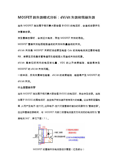
MOSFET的失效模式分析:dV/dt失效和雪崩失效当向MOSFET施加高于绝对最大额定值BVDSS的电压时,会造成击穿并引发雪崩击穿。
发生雪崩击穿时,会流过大电流,存在MOSFET失效的危险。
MOSFET雪崩失效包括短路造成的失效和热量造成的失效。
dV/dt失效是MOSFET关断时流经寄生电容Cds的充电电流流过基极电阻RB,使寄生双极晶体管导通而引起短路从而造成失效的现象。
dV/dt是单位时间内的电压变化量,VDS的上升坡度越陡,越容易发生MOSFET的dV/dt失效问题。
一般来说,反向恢复特性越差,dV/dt的坡度越陡,越容易产生MOSFET的dV/dt失效。
什么是雪崩击穿当向MOSFET施加高于绝对最大额定值BVDSS的电压时,就会发生击穿。
当施加高于BVDSS的高电场时,自由电子被加速并带有很大的能量。
这会导致碰撞电离,从而产生电子-空穴对。
这种电子-空穴对呈雪崩式增加的现象称为“雪崩击穿”。
在这种雪崩击穿期间,与MOSFET内部二极管电流呈反方向流动的电流称为“雪崩电流IAS”,参见下图(1)。
MOSFET的雪崩失效电流路径示意图(红色部分)雪崩失效:短路造成的失效如上图所示,IAS会流经MOSFET的基极寄生电阻RB。
此时,寄生双极型晶体管的基极和发射极之间会产生电位差VBE,如果该电位差较大,则寄生双极晶体管可能会变为导通状态。
一旦这个寄生双极晶体管导通,就会流过大电流,MOSFET可能会因短路而失效。
雪崩失效:热量造成的失效在雪崩击穿期间,不仅会发生由雪崩电流导致寄生双极晶体管误导通而造成的短路和损坏,还会发生由传导损耗带来的热量造成的损坏。
如前所述,当MOSFET处于击穿状态时会流过雪崩电流。
在这种状态下,BVDSS被施加到MOSFET并且流过雪崩电流,它们的乘积成为功率损耗。
这种功率损耗称为“雪崩能量EAS”。
雪崩测试电路及其测试结果的波形如下图所示。
此外,雪崩能量可以通过公式(1)来表示。

llc同步整流 mos管发热后电流波形不正常下载温馨提示:该文档是我店铺精心编制而成,希望大家下载以后,能够帮助大家解决实际的问题。
本文下载后可定制随意修改,请根据实际需要进行相应的调整和使用,谢谢!并且,本店铺为大家提供各种各样类型的实用资料,如教育随笔、日记赏析、句子摘抄、古诗大全、经典美文、话题作文、工作总结、词语解析、文案摘录、其他资料等等,如想了解不同资料格式和写法,敬请关注!Downloaded tips: This document is carefully compiled by the editor. I hope that after you download them, they can help you solve practical problems. The documents can be customized and modified after downloading, please adjust and use it according to actual needs, thank you!In addition, our shop provides you with various types of practical materials, such as educational essays, diary appreciation, sentence excerpts, ancient poems, classic articles, topic composition, work summary, word parsing, copy excerpts, other materials and so on, want to know different data formats and writing methods, please pay attention!LLC同步整流MOS管发热后电流波形不正常。
MOS失效的原因分析总结MOS管是金属(metal)—氧化物(oxide)—半导体(semiconductor)场效应晶体管,或者称是金属—绝缘体(insulator)—半导体。
MOS管的source和drain是可以对调的,他们都是在P型backgate中形成的N型区。
在多数情况下,这个两个区是一样的,即使两端对调也不会影响器件的性能。
这样的器件被认为是对称的。
目前在市场应用方面,排名第一的是消费类电子电源适配器产品。
而MOS管的应用领域排名第二的是计算机主板、NB、计算机类适配器、LCD显示器等产品,随着国情的发展计算机主板、计算机类适配器、LCD显示器对MOS管的需求有要超过消费类电子电源适配器的现象了。
第三的就属网络通信、工业控制、汽车电子以及电力设备领域了,这些产品对于MOS管的需求也是很大的,特别是现在汽车电子对于MOS管的需求直追消费类电子了。
下面对MOS失效的原因总结以下六点,然后对1,2重点进行分析:1:雪崩失效(电压失效),也就是我们常说的漏源间的BVdss电压超过MOSFET的额定电压,并且超过达到了一定的能力从而导致MOSFET失效。
2:SOA失效(电流失效),既超出MOSFET安全工作区引起失效,分为Id超出器件规格失效以及Id过大,损耗过高器件长时间热积累而导致的失效。
3:体二极管失效:在桥式、LLC等有用到体二极管进行续流的拓扑结构中,由于体二极管遭受破坏而导致的失效。
4:谐振失效:在并联使用的过程中,栅极及电路寄生参数导致震荡引起的失效。
5:静电失效:在秋冬季节,由于人体及设备静电而导致的器件失效。
6:栅极电压失效:由于栅极遭受异常电压尖峰,而导致栅极栅氧层失效。
雪崩失效分析(电压失效)到底什么是雪崩失效呢,简单来说MOSFET在电源板上由于母线电压、变压器反射电压、漏感尖峰电压等等系统电压叠加在MOSFET漏源之间,导致的一种失效模式。
简而言之就是由于就是MOSFET漏源极的电压超过其规定电压值并达到一定的能量限度而导致的一种常见的失效模式。
LLC谐振变换器中MOSFET失效模式分析1 摘要提高功率密度已经成为电源变换器的发展趋势。
为达到这个目标,需要提高开关频率,从而降低功率损耗、系统整体尺寸以及重量。
对于当今的开关电源(SMPS)而言,具有高可靠性也是非常重要的。
零电压开关(ZVS) 或零电流开关(ZCS) 拓扑允许采用高频开关技术,可以大限度地降低开关损耗。
ZVS拓扑允许工作在高频开关下,能够改善效率,能够降低应用的尺寸,还能够降低功率开关的应力,因此可以改善系统的可靠性。
LLC 谐振半桥变换器因其自身具有的多种优势逐渐成为一种主流拓扑。
这种拓扑得到了广泛的应用,包括高端服务器、平板显示器电源的应用。
但是,包含有LLC谐振半桥的ZVS 桥式拓扑,需要一个带有反向快速恢复体二极管的MOSFET,才能获得更高的可靠性。
在功率变换市场中,尤其对于通信/服务器电源应用,不断提高功率密度和追求更高效率已经成为具挑战性的议题。
对于功率密度的提高,普遍方法就是提高开关频率,以便降低无源器件的尺寸。
零电压开关(ZVS)拓扑因具有极低的开关损耗、较低的器件应力而允许采用高开关频率以及较小的外形,从而越来越受到青睐。
这些谐振变换器以正弦方式对能量进行处理,开关器件可实现软开闭,因此可以大大地降低开关损耗和噪声。
在这些拓扑中,相移ZVS全桥拓扑在中、高功率应用中得到了广泛采用,因为借助功率MOSFET的等效输出电容和变压器的漏感可以使所有的开关工作在ZVS 状态下,无需额外附加辅助开关。
然而,ZVS范围非常窄,续流电流消耗很高的循环能量。
近来,出现了关于相移全桥拓扑中功率MOSFET失效问题的讨论。
这种失效的主要原因是:在低反向电压下,MSOFET体二极管的反向恢复较慢。
另一失效原因是:空载或轻载情况下,出现Cdv/dt直通。
在LLC谐振变换器中的一个潜在失效模式与由于体二极管反向恢复特性较差引起的直通电流相关。
即使功率MOSFET的电压和电流处于安全工作区域,反向恢复dv/dt和击穿dv/dt也会在如启动、过载和输出短路的情况下发生。
MOSFETs are w ell know n to be prone to inexplicable failures - to the effect that the alternativ e expansion of the MOSFET acrony m is 'M agically O bliterated, S moke and F ire E mitting T ransistor'. The truth is that MOSFETs are incredibly robust - but that they fail v er y fast indeed if any of their rating are exceeded. There are a few ratings w hich are v er y difficult to get sensible info rmation on, and w hich can cause problems. This page (w hich can nev er be complete) is a start on try ing to explain some of these.Failure modesIt is alw ay s v er y difficult to be certain of exactly w hat caused any one failure: the problem is that failures are v er y difficult to promote in any w ell designed controller, and customers a re not usually aw are of exactly w hat happened to cause the failure. F urthermo re oncea MOSFET fails - it is now dud and w ill not w ork properly so it promptly goes into another failure mode, oblite rating the o riginalev idence. The examples here should be treated as helpful examples o nly - do not assume that, because y our MOSFET looks just likea particular e xample, then that is w hat caused the failure!Here are a few of the failure modes that can occur:1.Avalanche failure2.dV/dt failure (Motor brush noise)1.C auses and cures of motor noise2.A typical dV/dT failureExcess pow er dissipationExcess C urrent'F oreign' objects.Jammed (or blocked) moto rRapid acceleration/decele rationShort-circuited loadDud battery2Avalanche failureIf the maximum operating v oltage of a MOSFET is exceeded, it goes into Avalanche breakdow n. This is not necessarily destructi v e. The MOSFET specifications w ill state a maximum energy the MOSFET can take in av alanche mode. Energy is 1/2LI2 w here L is the inductance and I is the current. F ortunately, in most circuits, the energy the MOSFET may have to clamp is that contained in th e rather small (lumped) inductance of the batte ry and its leads. See the article on PWM controllers in the 4Q D TEC archives.If the energy contained in the transient ov er-v oltage is abov e the rated Av alanche energy level, then the MOSFET w ill fail. The dev ice fails short circuit, initially, w ith no externally v isible signs.The problem w ith this failure mode is that, once it o ccurs, there is likely to be a chain reaction w hich w ill probably disintegrate the MOSFET, obliterating the ev idence and probably blow ing other dev ices to boot. So it's of vital importance to report exactly w hat ev ents occurred at the point of failure.The controlle rs in no rmal use are gene rally incapable of generating spikes of enough ene rgy to blow them. So the necessa ry high energyspikes are usually generated by external events. These can be things such as:(1) C ontactors or re lay s sw itching (2) F uses blow ingTo prevent such failure, y ou need to understand not only how transients are generated, but also how they may trav el from gene ration point to the controlle r.dV/dt failureThis effect is probably the least understood and most my sterious of all MOSFET failures. It is also probably the biggest caus e of all those otherw ise inexplicable failures that let out the "Magic Smoke and F ire"! It is also one of the hardest failures to study as it is an extremely high-speed failure, so require s v er y expensiv e transient capture equipment. The good new s is that, as MOSFET technology improv es, it seems to be getting more ra re than once it w as!It is also a failure mode w hich is probably more common on industrial control sy stems. These tend to be w ired for neatness and appearance, so w ires tend to be longer than is ideal and routing tends to be bad. There are also sources of noise other than the motor, such as relay s and contacto rs. See the page on machine w iring.The cause of this failure is a v er y high v oltage, ver y fast transient spike (w hich may be positiv e or negative going). If such a spike gets onto the drain of a MOSFET, it gets coupled through the MOSFETs internal capacitance to the gate. If enough energy gets couple d, the v oltage on the gate rises abov e the maximum allow able lev el - and the MOSFET dies instantaneously. The process less than anano-second! The initial spike destroy s the gate-body insulatio n, so that the gate is co nnected to the body. O nce that has happene d, the MOSFET explodes in a cloud of flame and black smoke. We have one documented case w here the batter y w ire w orked loose, ca using a spark. It must have been this that caused the gate breakdow n for the explosion of flame and smoke did not happen until the ba ttery w ire w as re-connected some time later! Which demonstrates how v er y difficult cause and effect can be to connect!So w here can such a spike come from? Noise. Noise is generated by an arc - Marconi used an arc and a tuned circuit to first transmit a radio signal across the A tlantic ocean. A rcs are v er y good generators of w ide-band (random) noise. Random noise f rom an arc has a statistical probability of containing an e nergy spike of just the right parameters to blow a MOSFET. Whatev er y ou do - there is still a statistical probability, but y ou can reduce it to near v anishing point!Motor commutators and brush gear are arc genera tors: look at the brush gear on any motor and y ou w ill almost certainly see it arcing. May be you w onder how a motor controller ca n ev er w ork?Motors are probably at their noisiest w hen regenerating!How ev er much noise the motor actually generates, for it to cause damage the w iring has to be such that it can transmit a v er y fast (i.e. v er y high frequency) transient. Properly designed w iring w ill not do this but bad w iring can - if y ou are unlucky - act as a transmission line deliv ering the w hole energy of he transient back to the controller!Do not ov er-react here. Statistics are such that a properly designed motor controlle r can go on w orking continuously for y ears w ithout such a transient occurring. With production machines, the maker is using new, good condition motors. Noise is much le ss likel y here.5But may be it's y our controller that's next! Especially if (like many of our retail customers) y ou are using a second hand motor - w hich is much more likely to be w orn and noisy! Know ledge of w hat happens can help y ou reduce the probability!Causes and cures of motor noiseSince dV/dt failure is gene rally caused by noise generated by the motor brush gear, w hat faults and effects in the motor caus e no ise, and how can y ou reduce the problem?The follow ing problems cause or make motor noise w orse:∙Worn brushes and commutatorIf brush pressure is low or unev en, arcing w ill be greatly increased. A lw ay s make sure the motor commutator and brushes are in good condition.∙Dirt, especially metallic dirtDirt can get betw een commutator and brush, causing a rcing. Metallic particles espe cially are harmful as they can also short out segments of the commutator causing v er y bad arcing. So mask off the motor's v entilation w hile w orking on or near the machine and make sure dirt cannot ente r.∙Blocking the motorA blocked motor bounces and causes the brushes to behav e unpredictably.∙Over-revv ing the motor.C ommutators are mechanical sw itching dev ices. Depending on the motor's design (and other factors such as humidity andtemperature), there is a maximum f requency at w hich the design can sw itch. If y ou ov er-rev the motor (by apply ing an excess v oltage to it) the commutation w ill break dow n and a huge plasma field can be set up, short-circuiting the armature by way of an arc. This of course ca n easily destroy the controller! It w ill also not do the motor any good.Good things to do are:∙Take care in assemblingMotors are magnetic and can attract sw arf and metal dust. If this, or any abrasiv e dirt (for instance, fibreglass) gets into the motor, it w ill cause arcing and w ear. Seal any motor v ents w hile assembling the machine.∙Take care of the motor and general maintenance.A w ell cared for and maintained sy stem is alw ay s going to be more reliable. In particular, keep the motor and ele ctricsclean and dry and make sure the motor brushgea r and armature a re not w orn.∙Motor noise suppression.F it a 10n ceramic capacitors across the moto r brushes. This capacitor w ants to be a fairly high v oltage one as it w ill h av ea 20kHz squarew ave across it. This motor capacito r should be as close to the moto r's commutator as possible, ideally insidethe motor itself. If the motor is multi pole, fit (if y ou can) a separate capa citor across each pair of brushes. If y ou are h av ing these motors made for y ou, contact the motor manufacture r w ho may w ell offer such a capacitor as a productio n option. See also Radio C ontrolled Machines. General w iring hints.∙Good w iringProper lay out of w iring can help prev ent noise trav elling back from the motor to the controller. This is a large subject but there isa page on machine w iring.A typical dV/dT failure2 l j8 T; Z: p% ~3 d/ d& R4 qNCC01A ty pical dV/dT failure is show n in the 95kByte photo y ou get by clicking on the thumbnail, right. Note the black sooty deposit w here the MOSFET has 'flamed out' in a flash of flame and sooty smoke. You can see the erupted epoxy of the MOSFET. This controlle r w as returned to us w ith the statement "I had an ov erload on the motor". How ev er - it looks exactly like arc damage and it w as probably caused w hen the motor lead w as pulled off the motor terminal. There is clearly v isible melting of the motor term inal at bottom right, w hich can only hav e been done by the arc as the terminal w as pulled off, presumably in response to the motor getting jammed. It was this disconne ction that caused the failure rather than the stalled moto r.Excess power dissipation2 G+ i! H& W: q" n/ rExactly w hat happens depends on how excess the pow er is. It may be a sustained cooking. In this case, the MOSFET gets hot enough to literally unsolder itself. Much of the MO SFET heating at high currents is in the leads - w hich can quite easily unsolder themselv es w ithout the MOSFET failing! If the heat is generated in the chip, then it w ill get hot - but its maximum temperature is usually not silicon-restricted, but restricted by the fabrication. The silico n chip is bonded to the substrate by soft solder and it is quite easy to melt this and hav e it ooze betw een the epoxy and the metal of the body, forming solder droplets. This may w ell not destroy the chi p!3 c) f" B* L3 b- S& |Excess Cur rent+ f/ l1 l) Z5 ?+ `8 R; z1 _9 R% J+ |2 A, ?/ H/ k& {/ \Yes - if y ou put too much current through a MOSFET - it w ill fail. Exactly how it fails w ill depend on how high the excess current is and for how long it flow s and on the exact circumstances at the time. h5 N( k4 f* w2 h" jA ll controllers made by 4QD hav e a fast-acting current limit: this turns the speed dow n (or up if it's e xcess rege n braking current) so that the MOSF ET current is alw ay s w ell w ithin their safe handling ability.& {- i2 A* r$ M' ?6 u% G5 }+ Y- r, T) a P+ BPow er dissipation due to current is I2R - the current times the current times the resistance. But the heat dissipated is the pow er times the time, so I2R.t, there t is the time.If y ou slightly ov erload the MOSFET - it w ill get v er y hot. If y ou don't remov e the heat - the MOSFET w ill, quite literally, melt. At 60 amps, the leads on a TO220 (the commonest MOSFET housing) w ill literally unsolder themselv es. Though the current needed for t his depends on how long the leads are and how big an area of track they are soldered too. 4QD boards all hav e extra thick copper to act as a heatsink for the F ET leads.Then there is the inside of the MOSFET. The silicon chip can get v er y hot. It is bonded to the MOSFET's case w ith - soft solder. If you get the MOSFET hot enough, this solder bonding literally melts and oozes out betw een epox y of the case and the metal insert of the base. The MOSFET can easily be w orking after this - but of course its the rmal perfo rmance is shot as the soft solde r bond is damaged.Then if you really put too much current through, the internal bond w ires (w hich carry current from the external leads to the chip) fuse in a flash and explo de - probably forcing a chunk of epo xy into space a high speed. C ratered MOSFETs are not uncommon, but it's difficult to tell if this is from bond w ire explosion or the chip has exploded - both seem to occur pretty much in unison.For eign object failur eThe circuit of a controller does not and cannot include the effects of w ater, dirt, metal filing, stray nuts and bolts etc.Since the electrical propertie s of such o bjects cannot be defined, no r ca n their position in the circuit, it is v ery likely t hat any such extraneous material w ill cause malfunction and/or death of the controller.Since the MOSFETs do most of the w ork in the controller, they are the components most likely to suffer from such abuse!You must therefore house the contro ller to prev ent such occurrences. F urthermore, if 4Q D suspect such a ca use of failure, w e may not be prepared to se rv ice the controller.Jammed (or blocked) motorBlocking a motor is suddenly jamming it by means of a mechanical seizure or failure such that a rotating motor is v er y sudden ly stopped.O f course, y ou cannot bring a mechanical load, such as a rotating motor, to a sudden halt. Ev en if y ou throw a crow bar suddenly in the gears, much more happens than a sudden sto p! There w ill be bounce in the sy stem and the armature w ill certainly bounce. Probably the brushes w ill rock in their holders - there is alw ay s some clearance!A sudden increase on the ele ctrica l load as w ould be cause d by a straightforw ard, non-bouncy, seizure w ill simply engage the controlle r's current limit. Yes - the controller w ill quickly get hot, but y ou should have time to turn dow n the speed.A ny failure caused by blocking is likely to come because of the armature bounce: this w ill (of course) be at high current and w ill be accompanied by arcing at the commutator, so it w ill generate lots of ele ctrical noise. See dV/dt failure. Because this noise occurs at full current limit, it w ill likely be of high energy, so dangerous. Much depends on the motor, brush and commutator and the m echanics as w ell as the w iring.If y ou've read the ty pical dV/dT failure, abov e, you w ill also realise that the w orst thing y ou can do in the ev ent of a sudden jam is to pull off a motor lead! Turn dow n the speed, turn of the ignitio n, or if y ou must, disconnect the batte ry lead. Nev er disconne ct the motor lead!If y ou are making a machine w hich has mechanical travel limits - y ou hav e, of course, got electrical 'end stops' w hich slow the motor and stop it before it hits any mechanical limit...Rapid acceler ation/decelerationIf failure from blocking the motor occurs because of armature bounce, it must also be dangerous to apply too fast an accelera tion to a motor. A ny mechanical sy stem has a response time. If y ou tr y to accelerate the sy stem faster tha n this response time, y ou are 'shocking' it into a state w here there may w ell be a 'bounce'. This is one of the reasons w hy a controller alw ay s has an acce leration and deceleration ramp: for smooth take-up the pow er must alw ay s be applied to a mechanical sy stem slightly slow er than the sy stem can respo nd. A pply pow er faster than the sy stem's response time and y ou are, in effect, shock e xciting it! How ever - in most applications, the controller's current limit w ill engage if the acceleration is too fast, and this w ill apply an effectiv e ramp. So w e'v e nev er seen a failure that w e w ould care to attribute to this fault!Dud batteryIf the batter y voltage ev er falls too low, controller internal v oltage may fail and the sw itching may get confused. Of course controllers are designed not to do this unde r conceiv able and testable low voltage conditions.How ev er - batteries can sometimes fail in unpredictable w ay s. We hav e seen ones w ith faulty cells that go open circuit abov e a particula r curre nt. O f course, the current then falls to zero (as the cell is open-circuit) so the cell starts to oscillate.This sort of unpredictable battery fault is - unpredictable. So how to predict and test that it w on't damage the controller?So if y ou have problems, alw ay s get your battery properly tested at high discharge current. It should be able to supply more current than the controller's moto r current limit, w ithout show ing distress.Shor t-cir cuited loadIf the load is short-circuited, the current w ill rise and the curre nt limit w ill engage, so immediate failure w ill be prev ented. How ever - w e do not guarantee the co ntrolle rs are safe against sho rt circuits, for if the sho rt is sustained and is 'too short' - failure can ev entually occur.The current limit engages after about 2µSeconds. During these tw o microseconds, the MOSFET is sw itching on and 'feeling' the load. It is a period of extreme dissipation for the MOSFET. The MOSFET can sur v iv e this stress quite happily- but it gets extremely hot. If the load is too small, the MOSFET's insides w ill get hot enough that the heat cannot get out quickly enough and the soft-solder use d inside the package to bond it together w ill melt and ooze out betw een the base of the MOSFET and the insulator (y ou can usual ly see it on the insulato r afterw ards). The MOSFET w ill then fail.The time to failure is entirely dependant on the sev erity of the short-circuit, but is quite long enough for a human to react (30 secondsto sev eral minutes). How ev er the current and v oltage conditio ns in the MO SFET are entirely dependant on the w iring (both moto r and battery) as the motor is shorted o ut, so the time is comple tely unpredictableA uthor: Richard Torrens from 4Q D(1998-2013)F irst published: 26th F ebruary 2002.Last modified: 2013。