UCC561DPG4中文资料
- 格式:pdf
- 大小:196.85 KB
- 文档页数:8
作者郭益星F50设定:语言ENGLISHF51设定:机器类型:AUTOCOROF52设定:机器类型和单锭数:根据机器长度来设定240锭为240 ,有些原始值是216 ,每次停电如果电池没电会变回原始值F53设定:日期和时间F54设定:纱线支数系统一般设定为NECF55设定:换班时间F56设定:打开清纱器系统0是关1是开F57设定:检测头类型有两种MCK15 和MCK20 看机器上是哪种电清头,设定错误会造成乱切,运行过程中设定是要将F56变为0 ,并且查下F11里面的纱线支数和原料号数是否和原来设定的有变化,清纱设定F11设定:纱支号:支数,原料号材料系数棉为7.5 但要根据温湿度来设定,湿度越大纺棉时在7.5的基础上加起来,数字越大切的灵敏度会越低。
F12设定:引纱速度:机器的引纱速度纱疵通道S.L.TF13设定:清纱界限S.L.T (Mo)F20显示:监测到的纱疵F21显示:锁定的单锭F22显示:报警可以看到有哪些电清板有问题,或是电清上存在的问题,。
●MACH-START机器处于启动的状态,但必须有四个锭位同时纺纱超过一分钟●MONITORING OFF清纱器被关闭,见F56●...EU FAULTS某个评价单元有故障,见F23●...EU ERRORS通过自检确定了某块EU板有问题,见F62 F63 F64●SHORT CIRCUIT电压短路(+12V, -12V S%, L%, T%, Mo%, 支数),见F60●CONTROL VOLTAGE控制电压处于允许范围F23显示:有故障的评价单元:Error是错误的意思,MISSING 是代表没联系上,EU 是电清板的意思,DOUBLE 是表示是有一块电清板和这块电清板的地址码存在重复。
调好后如果还是这样,可以是拔码开关有问题F24显示:时钟33F25显示:Roda状态.6 木纹纱通道控制电压的监测F60显示:控制单元的电压:可以显示是哪种控制电压有问题。
561R and 564R SeriesVishay Cera-MiteDocument Number: 23115for technical questions, contact: ceramitesupport@Lower Voltage Ceramic Disc Capacitors 1 kV DC to 3 kV DC Low Dissipation FactorINSULATION RESISTANCEmin. 50 000 M ΩTOLERANCE ON CAPACITANCE± 5 %, ± 10 %DISSIPATION FACTOR0.1 % max. at 1 kHz; 1 VCATEGORY TEMPERATURE RANGE- 55 °C to + 125 °CCLIMATIC CATEGORY ACC. TO EN60068-155/125/21OPERATING TEMPERATURE RANGE- 55 °C to + 105 °CFEATURES•Low losses •High stability•Low DF minimizes self heating at HF •Ideal for high switching to 100 kHz •Radial leads•Compliant to RoHS directive 2002/95/ECAPPLICATIONS•SMPS •HF ballast•Snubber and HV cicuitsDESIGNThe capacitors consist of a ceramic disc of which both sides are silver-plated. Connection leads are made of tinned copper having diameters of 0.022" (0.51 mm) or 0.025"(0.64 mm).The capacitors may be supplied with radial kinked or straight leads having lead spacing of 0.250" (6.35 mm) or 0.375"(9.5 mm).The standard tolerances are ± 5 %, ± 10 %.Coating is made of or flammable retardant epoxy resin in accordance with “UL 94 V-0”.CAPACITANCE RANGE10 pF to 6800 pFRATED VOLTAGE1000 V DC (500 V RMS )2000 V DC (1000 V RMS )3000 V DC (1500 V RMS )DIELECTRIC STRENGTH BETWEEN LEADSComponent test:1000 V DC 2500V DC , 2 s 2000 V DC 4000 V DC , 2 s3000 V DC 6000V DC , 2 s CERAMIC DIELECTRICC0G, N1500, N2000, N2200, N2500, N2800 (Class 1)LEAD OFFSET 'LO' (NOMINAL)1 kV DC 0.045" (1.2 mm)2 kV DC 0.075" (1.4 mm)3 kV DC0.095" (1.8 mm) for technical questions, contact: ceramitesupport@Document Number: 23115561R and 564R SeriesVishay Cera-MiteLower Voltage Ceramic Disc Capacitors 1 kV DC to 3 kV DC Low Dissipation FactorNote• Alternate Lead Spacings of 5 mm, 7.5 mm or 10 mm are available on requestTAPE AND REEL OPTIONS• To specify tape and reel, add two letter suffix to the ordering code (for details of the packaging code see general section of the catalog)ORDERING INFORMATION, CERAMIC 1 kV DC LOW DISSIPATION FACTORC (pF)TOL.(%)DDIAMETER INCH (mm)TTHICKNESS INCH (mm)LSLEAD SPACE inch (mm)WIRE SIZE FIGORDERING CODEAWGINCH (mm)C0G (NP0)10± 5 %0.250 (6.4)0.156 (4.0)0.250 (6.4)220.025 (0.64)1561R1DF0Q1012561R1DF0Q12N150015± 5 %0.250 (6.4)0.156 (4.0)0.250 (6.4)220.025 (0.64)1561R1DF0Q1518561R1DF0Q1822561R1DF0Q2247561R1DF0Q4756561R1DF0Q5668561R1DF0Q6882561R1DF0Q82N220027± 10 %0.250 (6.4)0.156 (4.0)0.250 (6.4)220.025 (0.64)1561R1DF0Q2733561R1DF0Q3339561R1DF0Q39N2000100± 10 %0.250 (6.4)0.156 (4.0)0.250 (6.4)220.025 (0.64)1561R1DF0T10120561R1DF0T12150561R1DF0T15180561R1DF0T18N2500220± 10 %0.250 (6.4)0.156 (4.0)0.250 (6.4)220.025 (0.64)1561R1DF0T22270561R1DF0T27N2800330± 10 %0.250 (6.4)0.156 (4.0)0.250 (6.4)220.025 (0.64)1561R1DF0T33390561R1DF0T394700.290 (7.4)0.156 (4.0)0.250 (6.4)561R1DF0T47560561R1DF0T56680561R1DF0T68820561R1DF0T8210000.370 (9.4)0.156 (4.0)0.250 (6.4)561R1DF0D101200561R1DF0D1215000.405 (10.3)0.156 (4.0)0.250 (6.4)561R1DF0D1518000.440 (11.2)0.156 (4.0)0.250 (6.4)561R1DF0D1822000.460 (11.7)0.156 (4.0)0.250 (6.4)561R1DF0D222300561R1DF0D232400561R1DF0D242500561R1DF0D2527000.490 (12.4)0.156 (4.0)0.250 (6.4)561R1DF0D2733000.530 (13.5)0.156 (4.0)0.250 (6.4)561R1DF0D3339000.560 (14.2)0.156 (4.0)0.375 (9.5)561R1DF0D3947000.630 (16.0)0.156 (4.0)0.375 (9.5)561R1DF0D4768000.760 (19.3)0.156 (4.0)0.375 (9.5)561R1DF0D68Document Number: 23115for technical questions, contact: ceramitesupport@561R and 564R SeriesLower Voltage Ceramic Disc Capacitors 1 kV DC to 3 kV DC Low Dissipation FactorVishay Cera-MiteNote• Alternate Lead Spacings of 5 mm, 7.5 mm or 10 mm are available on requestTAPE AND REEL OPTIONS• To specify tape and reel, add two letter suffix to the ordering code (for details of the packaging code see general section of the catalog)ORDERING INFORMATION, CERAMIC 2 kV DC LOW DFC (pF)TOL.(%)DDIAMETER INCH (mm)TTHICKNESS INCH (mm)LSLEAD SPACE INCH (mm)WIRE SIZE FIG.ORDERING CODEAWG INCH (mm)C0G (NP0)10± 5 %0.290 (7.4)0.160 (4.1)0.250 (6.4)200.032 (0.81)1564R2DF0Q10N150012± 5 %0.290 (7.4)0.170 (4.3)0.250 (6.4)200.032 (0.81)1564R2DF0Q12270.290 (7.4)0.220 (5.6)0.250 (6.4)564R2DF0Q27330.290 (7.4)0.195 (5.0)0.250 (6.4)564R2DF0Q33390.290 (7.4)0.180 (4.6)0.250 (6.4)564R2DF0Q39470.290 (7.4)0.170 (4.3)0.250 (6.4)564R2DF0Q47N220015± 5 %0.290 (7.4)0.185 (4.7)0.250 (6.4)200.032 (0.81)1564R2DF0Q15180.290 (7.4)0.170 (4.3)0.250 (6.4)564R2DF0Q18220.290 (7.4)0.170 (4.3)0.250 (6.4)564R2DF0Q22N200056± 5 %0.290 (7.4)0.210 (5.3)0.250 (6.4)200.032 (0.81)1564R2DF0Q56680.290 (7.4)0.190 (4.8)0.250 (6.4)564R2DF0Q68820.290 (7.4)0.175 (4.5)0.250 (6.4)564R2DF0Q821000.290 (7.4)0.170 (4.3)0.250 (6.4)564R2DF0T10N2500120± 10 %0.290 (7.4)0.185 (4.7)0.250 (6.4)200.032 (0.81)1564R2DF0T121500.290 (7.4)0.170 (4.3)0.250 (6.4)564R2DF0T151800.290 (7.4)0.185 (4.7)0.250 (6.4)564R2DF0T182700.330 (8.4)0.170 (4.3)0.250 (6.4)564R2DF0T274700.400 (10.2)0.170 (4.3)0.250 (6.4)564R2DF0T47N2800220± 10 %0.290 (7.4)0.170 (4.3)0.250 (6.4)200.032 (0.81)1564R2DF0T223300.330 (8.4)0.185 (4.7)0.250 (6.4)564R2DF0T333900.330 (8.4)0.175 (4.5)0.250 (6.4)564R2DF0T395600.400 (10.2)0.185 (4.7)0.250 (6.4)564R2DF0T566800.400 (10.2)0.170 (4.3)0.250 (6.4)564R2DF0T688200.430 (10.9)0.175 (4.5)0.250 (6.4)564R2DF0T8210000.460 (11.7)0.170 (4.3)0.250 (6.4)564R2DF0D1012000.490 (12.5)0.170 (4.3)0.250 (6.4)564R2DF0D1215000.530 (13.5)0.170 (4.3)0.250 (6.4)564R2DF0D1518000.560 (14.2)0.170 (4.3)0.375 (9.5)564R2DF0D1822000.680 (17.3)0.180 (4.6)0.375 (9.5)564R2DF0D2223000.680 (17.3)0.175 (4.5)0.375 (9.5)564R2DF0D2324000.680 (17.3)0.175 (4.5)0.375 (9.5)564R2DF0D2425000.680 (17.3)0.170 (4.3)0.375 (9.5)564R2DF0D2527000.680 (17.3)0.170 (4.3)0.375 (9.5)564R2DF0D2733000.720 (18.3)0.170 (4.3)0.375 (9.5)564R2DF0D3339000.790 (20.1)0.170 (4.3)0.375 (9.5)564R2DF0D3947000.900 (22.9)0.180 (4.6)0.375 (9.5)564R2DF0D4756000.900 (22.9)0.170 (4.3)0.375 (9.5)564R2DF0D5668000.950 (24.1)0.170 (4.3)0.375 (9.5)564R2DF0D68 for technical questions, contact: ceramitesupport@Document Number: 23115561R and 564R SeriesVishay Cera-MiteLower Voltage Ceramic Disc Capacitors 1 kV DC to 3 kV DC Low Dissipation FactorNote• Alternate Lead Spacings of 5 mm, 7.5 mm or 10 mm are available on requestTAPE AND REEL OPTIONS• To specify tape and reel, add two letter suffix to the ordering code (for details of the packaging code see general section of the catalog)ORDERING INFORMATION, CERAMIC 3 kV DC LOW DFC (pF)TOL.(%)DDIAMETER INCH (mm)TTHICKNESS INCH (mm)LSLEAD SPACE INCH (mm)WIRE SIZE FIG.ORDERING CODEAWGINCH (mm)N150010± 5 %0.290 (7.4)0.185 (4.7)0.250 (6.4)200.032 (0.81)1564R3DF0Q10270.290 (7.4)0.220 (5.6)0.250 (6.4)564R3DF0Q27330.290 (7.4)0.195 (5.0)0.250 (6.4)564R3DF0Q33390.290 (7.4)0.190 (4.8)0.250 (6.4)564R3DF0Q39470.330 (8.4)0.225 (5.7)0.250 (6.4)564R3DF0Q47N220012± 5 %0.290 (7.4)0.210 (5.3)0.250 (6.4)200.032 (0.81)1564R3DF0Q12150.290 (7.4)0.185 (4.7)0.250 (6.4)564R3DF0Q15180.290 (7.4)0.185 (4.7)0.250 (6.4)564R3DF0Q18220.330 (8.4)0.210 (5.3)0.250 (6.4)564R3DF0Q22N200056± 5 %0.290 (7.4)0.210 (5.3)0.250 (6.4)200.032 (0.81)1564R3DF0Q56680.290 (7.4)0.190 (4.8)0.250 (6.4)564R3DF0Q68820.290 (7.4)0.185 (4.7)0.250 (6.4)564R3DF0Q82N2500100± 10 %0.290 (7.4)0.205 (5.2)0.250 (6.4)200.032 (0.81)1564R3DF0T101200.290 (7.4)0.190 (4.8)0.250 (6.4)564R3DF0T122200.330 (8.4)0.190 (4.8)0.250 (6.4)564R3DF0T22N2800150± 10 %0.290 (7.4)0.200 (5.1)0.250 (6.4)200.032 (0.81)1564R3DF0T151800.290 (7.4)0.190 (4.8)0.250 (6.4)564R3DF0T182700.330 (8.4)0.205 (5.2)0.250 (6.4)564R3DF0T273300.330 (8.4)0.190 (4.8)0.250 (6.4)564R3DF0T333900.400 (10.2)0.215 (5.5)0.250 (6.4)564R3DF0T394700.400 (10.2)0.195 (5.0)0.250 (6.4)564R3DF0T475600.430 (10.9)0.200 (5.1)0.250 (6.4)564R3DF0T566800.460 (11.7)0.195 (5.0)0.250 (6.4)564R3DF0T688200.490 (12.5)0.195 (5.0)0.250 (6.4)564R3DF0T8210000.530 (13.5)0.190 (4.8)0.250 (6.4)564R3DF0D1012000.560 (14.2)0.190 (4.8)0.375 (9.5)564R3DF0D1215000.620 (15.8)0.190 (4.8)0.375 (9.5)564R3DF0D1518000.680 (17.3)0.190 (4.8)0.375 (9.5)564R3DF0D1822000.720 (18.3)0.190 (4.8)0.375 (9.5)564R3DF0D2223000.720 (18.3)0.190 (4.8)0.375 (9.5)564R3DF0D2324000.790 (20.1)0.195 (5.0)0.375 (9.5)564R3DF0D2425000.790 (20.1)0.195 (5.0)0.375 (9.5)564R3DF0D2527000.790 (20.1)0.190 (4.8)0.375 (9.5)564R3DF0D2733000.900 (22.9)0.200 (5.1)0.375 (9.5)564R3DF0D3339000.900 (22.9)0.190 (4.8)0.375 (9.5)564R3DF0D3947000.950 (24.1)0.185 (4.7)0.375 (9.5)564R3DF0D47Document Number: 23115for technical questions, contact: ceramitesupport@561R and 564R SeriesLower Voltage Ceramic Disc Capacitors 1 kV DC to 3 kV DC Low Dissipation FactorVishay Cera-MiteNote 1Power ratings are based on still air 60 °C ambient with additional 30 °C rise due to self heating.Thermal effects such as forced air cooling, component encapsulation or other heat-sinking techniques will alter ratings.Actual circuit for application recommended.Note 2For convienience, power rating charts are shown to 100 kHz.Higher frequency operation is permissible with appropriate derating.Consult us for application suggestions.Legal Disclaimer Notice VishayDisclaimerALL PRODU CT, PRODU CT SPECIFICATIONS AND DATA ARE SU BJECT TO CHANGE WITHOU T NOTICE TO IMPROVE RELIABILITY, FUNCTION OR DESIGN OR OTHERWISE.Vishay Intertechnology, Inc., its affiliates, agents, and employees, and all persons acting on its or their behalf (collectively,“Vishay”), disclaim any and all liability for any errors, inaccuracies or incompleteness contained in any datasheet or in any other disclosure relating to any product.Vishay makes no warranty, representation or guarantee regarding the suitability of the products for any particular purpose or the continuing production of any product. To the maximum extent permitted by applicable law, Vishay disclaims (i) any and all liability arising out of the application or use of any product, (ii) any and all liability, including without limitation special, consequential or incidental damages, and (iii) any and all implied warranties, including warranties of fitness for particular purpose, non-infringement and merchantability.Statements regarding the suitability of products for certain types of applications are based on Vishay’s knowledge of typical requirements that are often placed on Vishay products in generic applications. Such statements are not binding statements about the suitability of products for a particular application. It is the customer’s responsibility to validate that a particular product with the properties described in the product specification is suitable for use in a particular application. Parameters provided in datasheets and/or specifications may vary in different applications and performance may vary over time. All operating parameters, including typical parameters, must be validated for each customer application by the customer’s technical experts. Product specifications do not expand or otherwise modify Vishay’s terms and conditions of purchase, including but not limited to the warranty expressed therein.Except as expressly indicated in writing, Vishay products are not designed for use in medical, life-saving, or life-sustaining applications or for any other application in which the failure of the Vishay product could result in personal injury or death. Customers using or selling Vishay products not expressly indicated for use in such applications do so at their own risk and agree to fully indemnify and hold Vishay and its distributors harmless from and against any and all claims, liabilities, expenses and damages arising or resulting in connection with such use or sale, including attorneys fees, even if such claim alleges that Vishay or its distributor was negligent regarding the design or manufacture of the part. Please contact authorized Vishay personnel to obtain written terms and conditions regarding products designed for such applications.No license, express or implied, by estoppel or otherwise, to any intellectual property rights is granted by this document or by any conduct of Vishay. Product names and markings noted herein may be trademarks of their respective owners.Material Category PolicyVishay Intertechnology, Inc. hereb y certifies that all its products that are identified as RoHS-Compliant fulfill the definitions and restrictions defined under Directive 2011/65/EU of The European Parliament and of the Council of June 8, 2011 on the restriction of the use of certain hazardous substances in electrical and electronic equipment (EEE) - recast, unless otherwise specified as non-compliant.Please note that some Vishay documentation may still make reference to RoHS Directive 2002/95/EC. We confirm that all the products identified as being compliant to Directive 2002/95/EC conform to Directive 2011/65/EU.Revision: 12-Mar-121Document Number: 91000分销商库存信息:VISHAY-BC-COMPONENTS561R1DF0T82561R1DF0T68561R1DF0T56 561R1DF0T47561R1DF0T39561R1DF0T33 561R1DF0T27561R1DF0T22561R1DF0T18 561R1DF0T15561R1DF0T12561R1DF0T10 561R1DF0Q82561R1DF0Q68561R1DF0Q56 561R1DF0Q47561R1DF0Q39561R1DF0Q33 561R1DF0Q27561R1DF0Q22564R3DF0T22 564R2DF0T39564R2DF0T33564R2DF0T27 561R1DF0Q12561R1DF0Q10561R1DF0D10 561R1DF0D18561R1DF0D12564R2DF0T68 564R2DF0T56564R2DF0T47564R3DF0T18 564R3DF0T10564R3DF0Q68564R3DF0Q33 564R3DF0Q10564R2DF0T22564R2DF0T18 564R2DF0T15564R2DF0T12564R2DF0T10 564R2DF0Q82564R2DF0Q68564R2DF0Q56 564R2DF0Q47564R2DF0Q39561R1DF0D39 561R1DF0D33561R1DF0Q15564R3DF0D10 561R1DF0D24561R1DF0D23561R1DF0D22 564R3DF0T68564R3DF0T56564R3DF0D18 564R2DF0D27564R2DF0D22561R1DF0D47 564R3DF0T39564R2DF0T82564R2DF0D10 564R2DF0D25564R3DF0D12564R2DF0D18 561R1DF0Q18564R3DF0T15564R3DF0T12 564R3DF0Q82564R3DF0Q56564R2DF0Q33 564R2DF0Q27564R2DF0Q22564R2DF0Q18 564R2DF0Q15564R2DF0Q12564R2DF0Q10 564R3DF0D15564R3DF0T82564R2DF0D12 564R3DF0T47564R3DF0T33564R3DF0T27 564R3DF0Q47564R2DF0D15564R2DF0D23 561R1DF0D56564R3DF0D23564R2DF0D24 564R3DF0Q39564R3DF0D39564R2DF0D56 564R3DF0D33564R2DF0D47564R3DF0D47 564R2DF0D68。
奈特科尔d4中文说明书
1、接通电源后,显示器显示软件版本号d4-0802
数秒后进入工作状态。
在显示
版本号期间,6个状态指示灯应全部不亮,否则表示仪表自检有故障。
“净重”灯亮----表示面板按键可能有故障。
“日期”灯亮―---表示实时时钟错误。
2、通过“标定”中的“参数设置”可设置“oFF”即自动关断电源时间(出厂设置为
10分钟)
(1)、使用交流电时不自动关机(2)、每次按键时关机时间重新计时
(3)、秤上有载荷且不稳定时关机时间重新计时
3、自动关机后仪表仍耗电约1mA,所以如果几天不用,应该切断仪表背面的电源开关
或拔下电池插头。
4、自动关机后重新开机的方法是,将仪表背面的电源开关关闭约2秒后,再接通开
关。
5、仪表关闭电源开关、自动关机、微型打印机打印中,欠电指示灯亮是正常的。
6、仪表背面的电源开关不影响充电。
7、第一次或长期未用的电池,在使用前应充满电。
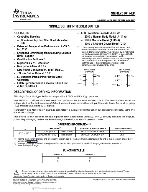
FEATURESNC V CCYAGNDDCK PACKAGE(TOP VIEW)DBV PACKAGE(TOP VIEW)NCAGNDV CCY DESCRIPTION/ORDERING INFORMATIONSN74LVC1G17-EPSGLS336A–APRIL2006–REVISED JUNE2007SINGLE SCHMITT-TRIGGER BUFFER•ESD Protection Exceeds JESD22•Controlled Baseline–2000-V Human-Body Model(A114-A)–One Assembly/Test Site,One Fabrication–200-V Machine Model(A115-A) Site–1000-V Charged-Device Model(C101)•Extended Temperature Performance of–55°C(1)Component qualification in accordance with JEDEC andto125°C industry standards to ensure reliable operation over anextended temperature range.This includes,but is not limited •Enhanced Diminishing Manufacturing Sources to,Highly Accelerated Stress Test(HAST)or biased85/85,(DMS)Support temperature cycle,autoclave or unbiased HAST,electromigration,bond intermetallic life,and mold compound •Qualification Pedigree(1)life.Such qualification testing should not be viewed asjustifying use of this component beyond specified •Supports5-V V CC Operationperformance and environmental limits.•Max tpd of4.6ns at3.3V•Low Power Consumption,10μA Max I CC•±24mA Output Drive at3.3V•I off Supports Partial Power Down ModeOperation•Latch-Up Performance Exceeds100mA PerJESD78,Class IIThis single Schmitt-trigger buffer is designed for1.65-V to5.5-V V CC operation.The SN74LVC1G17contains one buffer and performs the Boolean function Y=A.The device functions as an independent buffer,but because of Schmitt action,it may have different input threshold levels for positive-going (V T+)and negative-going(V T–)signals.NanoStar™and NanoFree™package technology is a major breakthrough in IC packaging concepts,using the die as the package.This device is fully specified for partial-power-down applications using I off.The I off circuitry disables the outputs, preventing damaging current backflow through the device when it is powered down.ORDERING INFORMATION(1)T A PACKAGE(2)ORDERABLE PART NUMBER TOP-SIDE MARKINGSOT(SC-70)-DCK Reel of3000SN74LVC1G17MDCKREP C70–55°C to125°CSOP(SOT-23)-DBV Reel of3000SN74LVC1G17MDBVREP C170(1)For the most current package and ordering information,see the Package Option Addendum at the end of this document,or see the TIwebsite at .(2)Package packing quantities,thermal data,symbolization,and PCB design guidelines are available at/sc/package.FUNCTION TABLEINPUT A OUTPUT YH HL LPlease be aware that an important notice concerning availability,standard warranty,and use in critical applications of TexasInstruments semiconductor products and disclaimers thereto appears at the end of this data sheet.NanoStar,NanoFree are trademarks of Texas Instruments.PRODUCTION DATA information is current as of publication date.Copyright©2006–2007,Texas Instruments Incorporated Products conform to specifications per the terms of the TexasInstruments standard warranty.Production processing does notnecessarily include testing of all parameters.AYABSOLUTE MAXIMUM RATINGSRECOMMENDED OPERATING CONDITIONS (1)SN74LVC1G17-EPSGLS336A–APRIL 2006–REVISED JUNE 2007LOGIC DIAGARAM (POSITIVE LOGIC)over operating free-air temperature range (unless otherwise noted)(1)VALUE UNIT V CC Supply voltage range –0.5to 6.5V V I Input voltage range (2)–0.5to 6.5V Voltage range applied to any output in the high-impedance or power-off state –0.5to 6.5V V O Voltage range applied to any output in the high or low state (2)(3)–0.5to V CC +0.5V I IK Input clamp current (V I <0)–50mA I OK Output clamp current (V O <0)-50mA I O Continuous output current±50mA Continuous current through V CC or GND ±100mA θJA Package thermal impedance (4):DCK package252°C/W T stg Storage temperature range–65to 150°C(1)Stresses beyond those listed under absolute maximum ratings may cause permanent damage to the device.These are stress ratings only,and functional operation of the device at these or any other conditions beyond those indicated under recommended operating conditions is not implied.Exposure to absolute-maximum-rated conditions for extended periods may affect device reliability.(2)The input and output negative-voltage ratings may be exceeded if the input and output current ratings are observed.(3)The value of V CC is provided in the recommended operating conditions table.(4)The package thermal impedance is calculated in accordance with JESD 51-7.MAXMAX UNIT Operating1.65 5.5V CC Supply voltage V Data retention only1.5V I Input voltage 0 5.5V V OOutput voltageV CC VV CC =1.65V –4V CC =2.3V–8I OHHigh–16mAV CC =3V –24V CC =4.5V –32V CC =1.65V 4V CC =2.3V8I OLLow-level output current16mA V CC =3V 24V CC =4.5V32T A Operating free-air temperature–55125°C (1)All unused inputs of the device must be held at V CC or GND to ensure proper device operation.See the TI application report,Implications of Slow or Floating CMOS Inputs (SCBA004).2Submit Documentation FeedbackELECTRICAL CHARACTERISTICSSN74LVC1G17-EP SGLS336A–APRIL2006–REVISED JUNE2007over operating free-air temperature range(unless otherwise noted)PARAMETER TEST CONDITIONS V CC MIN TYP(1)MAX UNIT1.65V to4.5V0.76 1.132.3V 1.08 1.56Positive-going inputV T+3V 1.48 1.92V threshold voltage4.5V 2.19 2.745.5V 2.65 3.331.65V to4.5V0.350.592.3V0.560.88Negative-goingV T–input threshold3V0.89 1.2V voltage 4.5V 1.51 1.975.5V 1.88 2.41.65V to4.5V0.360.64ΔV<S 2.3V0.450.78ubscri Hysteresis3V0.510.83V pt>T</(V T+–V T–)4.5V0.580.93Subscript> 5.5V0.69 1.04I OH=–100mA 1.65V to4.5V V CC–0.1I OH=-4mA 1.65V 1.2I OH=–8mA 2.3V 1.9V OH VI OH=–16mA 2.43VI OH=–24mA 2.3I OH=–32mA 4.5V 3.8I OL=100mA 1.65V to4.5V0.1I OL=4mA 1.65V0.45I OL=8mA 2.3V0.3V OL VI OL=16mA0.43VI OL=24mA0.55I OL=32mA 4.5V0.55I I A input V I=5.5or GND0to5.5V±5μAI off V I or V O=5.5V0±10μAI CC V I=5.5V or GND,I O=0 1.65V to5.5V10μAOne input at V CC–0.6V,ΔI CC3V to5.5V500μA Other inputs at V CC or GNDC i V I=V CC or GND 3.3V 4.5pF(1)All typical values are at V CC=3.3V,T A=25°C.3Submit Documentation FeedbackSWITCHING CHARACTERISTICSSWITCHING CHARACTERISTICSOPERATING CHARACTERISTICS,SN74LVC1G17-EPSGLS336A–APRIL 2006–REVISED JUNE 2007over recommended operating free-air temperature range,C L =15pF (unless otherwise noted)(see Figure 1)V CC =1.8V V CC =2.5V V CC =3.3V V CC =5V FROM TO ±0.15V ±0.2V ±0.3V ±0.5V PARAMETERUNIT(INPUT)(OUTPUT)MIN MAX MIN MAX MIN MAX MIN MAX t pdAY2.89.91.65.51.54.60.94.4ns over recommended operating free-air temperature range,C L =30pF or 50pF (unless otherwise noted)(see Figure 2)V CC =1.8V V CC =2.5V V CC =3.3V V CC =5V FROM TO ±0.15V ±0.2V ±0.3V ±0.5V PARAMETERUNIT(INPUT)(OUTPUT)MIN MAX MIN MAX MIN MAX MIN MAXt pdAY3.81126.51.85.51.25ns T A =25°CV CC =1.8VV CC =2.5VV CC =3.3VV CC =5V PARAMETERTEST CONDITIONSUNITTYP TYP TYP TYP C pd Power dissipaton capacitancef =10MHz202122264Submit Documentation FeedbackPARAMETER MEASUREMENT INFORMATIONFrom Output Under TestLOAD CIRCUITOpen Data InputTiming InputV I0 VV I0 V0 VInputVOLTAGE WAVEFORMS SETUP AND HOLD TIMESVOLTAGE WAVEFORMS PROPAGATION DELAY TIMESINVERTING AND NONINVERTING OUTPUTSVOLTAGE WAVEFORMS PULSE DURATIONV OHV OHV OLV OLV I0 V InputOutput Waveform 1S1 at V LOAD (see Note B)Output Waveform 2S1 at GND (see Note B)V OLV OH V LOAD /20 V≈0 VV IVOLTAGE WAVEFORMS ENABLE AND DISABLE TIMES LOW- AND HIGH-LEVEL ENABLINGOutputOutputt PLH /t PHL t PLZ /t PZL t PHZ /t PZHOpen V LOAD GNDTEST S1NOTES: A.C L includes probe and jig capacitance.B.Waveform 1 is for an output with internal conditions such that the output is low, except when disabled by the output control.Waveform 2 is for an output with internal conditions such that the output is high, except when disabled by the output control.C.All input pulses are supplied by generators having the following characteristics: PRR ≤ 10 MHz, Z O = 50 Ω.D.The outputs are measured one at a time, with one transition per measurement.E.t PLZ and t PHZ are the same as t dis .F.t PZL and t PZH are the same as t en .G.t PLH and t PHL are the same as t pd .H.All parameters and waveforms are not applicable to all devices.Output Control V I1.8 V ± 0.15 V2.5 V ± 0.2 V3.3 V ± 0.3 V 5 V ± 0.5 V1 M Ω1 M Ω1 M Ω1 M ΩV CC R L 2 × V CC 2 × V CC 6 V 2 × V CCV LOAD C L 15 pF 15 pF 15 pF 15 pF0.15 V 0.15 V 0.3 V 0.3 VV ∆V CC V CC 3 V V CCV I V CC /2V CC /21.5 V V CC /2V M t r /t f ≤2 ns ≤2 ns ≤2.5 ns ≤2.5 nsINPUTS SN74LVC1G17-EPSGLS336A–APRIL 2006–REVISED JUNE 2007Figure 1.Load Circuit and Voltage Waveforms5Submit Documentation FeedbackFrom Output Under TestLOAD CIRCUITOpen Data InputTiming InputV I0 VV I0 V0 VInputVOLTAGE WAVEFORMS SETUP AND HOLD TIMESVOLTAGE WAVEFORMS PROPAGATION DELAY TIMESINVERTING AND NONINVERTING OUTPUTSVOLTAGE WAVEFORMS PULSE DURATIONV OHV OHV OLV OLV I0 V InputOutput Waveform 1S1 at V LOAD (see Note B)Output Waveform 2S1 at GND (see Note B)V OLV OH V LOAD /20 V≈0 VV IVOLTAGE WAVEFORMS ENABLE AND DISABLE TIMES LOW- AND HIGH-LEVEL ENABLINGOutputOutputt PLH /t PHL t PLZ /t PZL t PHZ /t PZHOpen V LOAD GNDTEST S1NOTES: A.C L includes probe and jig capacitance.B.Waveform 1 is for an output with internal conditions such that the output is low, except when disabled by the output control.Waveform 2 is for an output with internal conditions such that the output is high, except when disabled by the output control.C.All input pulses are supplied by generators having the following characteristics: PRR ≤ 10 MHz, Z O = 50 Ω.D.The outputs are measured one at a time, with one transition per measurement.E.t PLZ and t PHZ are the same as t dis .F.t PZL and t PZH are the same as t en .G.t PLH and t PHL are the same as t pd .H.All parameters and waveforms are not applicable to all devices.Output Control V I1.8 V ± 0.15 V2.5 V ± 0.2 V3.3 V ± 0.3 V 5 V ± 0.5 V1 k Ω500 Ω500 Ω500 ΩV CC R L 2 × V CC 2 × V CC 6 V 2 × V CCV LOAD C L 30 pF 30 pF 50 pF 50 pF0.15 V 0.15 V 0.3 V 0.3 VV ∆V CC V CC 3 V V CCV I V CC /2V CC /21.5 V V CC /2V M t r /t f ≤2 ns ≤2 ns ≤2.5 ns ≤2.5 nsINPUTS SN74LVC1G17-EPSGLS336A–APRIL 2006–REVISED JUNE 2007PARAMETER MEASUREMENT INFORMATION (continued)Figure 2.Load Circuit and Voltage Waveforms6Submit Documentation FeedbackAddendum-Page 1PACKAGING INFORMATIONOrderable Device Status(1)Package Type PackageDrawingPins Package QtyEco Plan(2)Lead/Ball FinishMSL Peak Temp(3)Samples (Requires Login)CLVC1G17MDCKREPG4ACTIVE SC70DCK 53000Green (RoHS & no Sb/Br)CU NIPDAU Level-1-260C-UNLIM Contact TI Distributor or Sales Office SN74LVC1G17MDBVREP ACTIVE SOT-23DBV 53000Green (RoHS & no Sb/Br)CU NIPDAU Level-1-260C-UNLIM Contact TI Distributor or Sales Office SN74LVC1G17MDCKREPACTIVE SC70DCK 53000Green (RoHS & no Sb/Br)CU NIPDAU Level-1-260C-UNLIM Contact TI Distributor or Sales Office V62/06621-01XE ACTIVE SOT-23DBV 53000Green (RoHS & no Sb/Br)CU NIPDAU Level-1-260C-UNLIM Contact TI Distributor or Sales Office V62/06621-01YEACTIVESC70DCK53000Green (RoHS & no Sb/Br)CU NIPDAU Level-1-260C-UNLIMContact TI Distributor or Sales Office(1)The marketing status values are defined as follows:ACTIVE: Product device recommended for new designs.LIFEBUY: TI has announced that the device will be discontinued, and a lifetime-buy period is in effect.NRND: Not recommended for new designs. Device is in production to support existing customers, but TI does not recommend using this part in a new design.PREVIEW: Device has been announced but is not in production. Samples may or may not be available.OBSOLETE: TI has discontinued the production of the device.(2)Eco Plan - The planned eco-friendly classification: Pb-Free (RoHS), Pb-Free (RoHS Exempt), or Green (RoHS & no Sb/Br) - please check /productcontent for the latest availability information and additional product content details.TBD: The Pb-Free/Green conversion plan has not been defined.Pb-Free (RoHS): TI's terms "Lead-Free" or "Pb-Free" mean semiconductor products that are compatible with the current RoHS requirements for all 6 substances, including the requirement that lead not exceed 0.1% by weight in homogeneous materials. Where designed to be soldered at high temperatures, TI Pb-Free products are suitable for use in specified lead-free processes.Pb-Free (RoHS Exempt): This component has a RoHS exemption for either 1) lead-based flip-chip solder bumps used between the die and package, or 2) lead-based die adhesive used between the die and leadframe. The component is otherwise considered Pb-Free (RoHS compatible) as defined above.Green (RoHS & no Sb/Br): TI defines "Green" to mean Pb-Free (RoHS compatible), and free of Bromine (Br) and Antimony (Sb) based flame retardants (Br or Sb do not exceed 0.1% by weight in homogeneous material)(3)MSL, Peak Temp. -- The Moisture Sensitivity Level rating according to the JEDEC industry standard classifications, and peak solder temperature.Important Information and Disclaimer:The information provided on this page represents TI's knowledge and belief as of the date that it is provided. TI bases its knowledge and belief on information provided by third parties, and makes no representation or warranty as to the accuracy of such information. Efforts are underway to better integrate information from third parties. TI has taken and continues to take reasonable steps to provide representative and accurate information but may not have conducted destructive testing or chemical analysis on incoming materials and chemicals.TI and TI suppliers consider certain information to be proprietary, and thus CAS numbers and other limited information may not be available for release.In no event shall TI's liability arising out of such information exceed the total purchase price of the TI part(s) at issue in this document sold by TI to Customer on an annual basis.芯天下--/OTHER QUALIFIED VERSIONS OF SN74LVC1G17-EP :•Catalog: SN74LVC1G17•Automotive: SN74LVC1G17-Q1NOTE: Qualified Version Definitions:•Catalog - TI's standard catalog product•Automotive - Q100 devices qualified for high-reliability automotive applications targeting zero defectsAddendum-Page 2芯天下--/TAPE AND REEL INFORMATION*All dimensions are nominalDevicePackage Type Package DrawingPins SPQReel Diameter (mm)Reel Width W1(mm)A0(mm)B0(mm)K0(mm)P1(mm)W (mm)Pin1Quadrant SN74LVC1G17MDBVREP SOT-23DBV 53000179.08.4 3.2 3.2 1.4 4.08.0Q3SN74LVC1G17MDCKREPSC70DCK53000179.08.42.22.51.24.08.0Q3*All dimensions are nominalDevice Package Type Package Drawing Pins SPQ Length(mm)Width(mm)Height(mm) SN74LVC1G17MDBVREP SOT-23DBV53000203.0203.035.0SN74LVC1G17MDCKREP SC70DCK53000203.0203.035.0IMPORTANT NOTICETexas Instruments Incorporated and its subsidiaries(TI)reserve the right to make corrections,modifications,enhancements,improvements, and other changes to its products and services at any time and to discontinue any product or service without notice.Customers should obtain the latest relevant information before placing orders and should verify that such information is current and complete.All products are sold subject to TI’s terms and conditions of sale supplied at the time of order acknowledgment.TI warrants performance of its hardware products to the specifications applicable at the time of sale in accordance with TI’s standard warranty.Testing and other quality control techniques are used to the extent TI deems necessary to support this warranty.Except where mandated by government requirements,testing of all parameters of each product is not necessarily performed.TI assumes no liability for applications assistance or customer product design.Customers are responsible for their products and applications using TI components.To minimize the risks associated with customer products and applications,customers should provide adequate design and operating safeguards.TI does not warrant or represent that any license,either express or implied,is granted under any TI patent right,copyright,mask work right, or other TI intellectual property right relating to any combination,machine,or process in which TI products or services are rmation published by TI regarding third-party products or services does not constitute a license from TI to use such products or services or a warranty or endorsement e of such information may require a license from a third party under the patents or other intellectual property of the third party,or a license from TI under the patents or other intellectual property of TI.Reproduction of TI information in TI data books or data sheets is permissible only if reproduction is without alteration and is accompanied by all associated warranties,conditions,limitations,and notices.Reproduction of this information with alteration is an unfair and deceptive business practice.TI is not responsible or liable for such altered rmation of third parties may be subject to additional restrictions.Resale of TI products or services with statements different from or beyond the parameters stated by TI for that product or service voids all express and any implied warranties for the associated TI product or service and is an unfair and deceptive business practice.TI is not responsible or liable for any such statements.TI products are not authorized for use in safety-critical applications(such as life support)where a failure of the TI product would reasonably be expected to cause severe personal injury or death,unless officers of the parties have executed an agreement specifically governing such use.Buyers represent that they have all necessary expertise in the safety and regulatory ramifications of their applications,and acknowledge and agree that they are solely responsible for all legal,regulatory and safety-related requirements concerning their products and any use of TI products in such safety-critical applications,notwithstanding any applications-related information or support that may be provided by TI.Further,Buyers must fully indemnify TI and its representatives against any damages arising out of the use of TI products in such safety-critical applications.TI products are neither designed nor intended for use in military/aerospace applications or environments unless the TI products are specifically designated by TI as military-grade or"enhanced plastic."Only products designated by TI as military-grade meet military specifications.Buyers acknowledge and agree that any such use of TI products which TI has not designated as military-grade is solely at the Buyer's risk,and that they are solely responsible for compliance with all legal and regulatory requirements in connection with such use. TI products are neither designed nor intended for use in automotive applications or environments unless the specific TI products are designated by TI as compliant with ISO/TS16949requirements.Buyers acknowledge and agree that,if they use any non-designated products in automotive applications,TI will not be responsible for any failure to meet such requirements.Following are URLs where you can obtain information on other Texas Instruments products and application solutions:Products ApplicationsAudio /audio Communications and Telecom /communicationsAmplifiers Computers and Peripherals /computersData Converters Consumer Electronics /consumer-appsDLP®Products Energy and Lighting /energyDSP Industrial /industrialClocks and Timers /clocks Medical /medicalInterface Security /securityLogic Space,Avionics and Defense /space-avionics-defense Power Mgmt Transportation and /automotiveAutomotiveMicrocontrollers Video and Imaging /videoRFID Wireless /wireless-appsRF/IF and ZigBee®Solutions /lprfTI E2E Community Home Page Mailing Address:Texas Instruments,Post Office Box655303,Dallas,Texas75265Copyright©2011,Texas Instruments Incorporated。
PACKAGING INFORMATIONOrderable Device Status(1)PackageType PackageDrawingPins PackageQtyEco Plan(2)Lead/Ball Finish MSL Peak Temp(3)UCC2813D-0ACTIVE SOIC D875Green(RoHS&no Sb/Br)CU NIPDAU Level-1-260C-UNLIMUCC2813D-0G4ACTIVE SOIC D875Green(RoHS&no Sb/Br)CU NIPDAU Level-1-260C-UNLIMUCC2813D-1ACTIVE SOIC D875Green(RoHS&no Sb/Br)CU NIPDAU Level-1-260C-UNLIMUCC2813D-1G4ACTIVE SOIC D875Green(RoHS&no Sb/Br)CU NIPDAU Level-1-260C-UNLIMUCC2813D-2ACTIVE SOIC D875Green(RoHS&no Sb/Br)CU NIPDAU Level-1-260C-UNLIMUCC2813D-2G4ACTIVE SOIC D875Green(RoHS&no Sb/Br)CU NIPDAU Level-1-260C-UNLIMUCC2813D-3ACTIVE SOIC D875Green(RoHS&no Sb/Br)CU NIPDAU Level-1-260C-UNLIMUCC2813D-3G4ACTIVE SOIC D875Green(RoHS&no Sb/Br)CU NIPDAU Level-1-260C-UNLIMUCC2813D-4ACTIVE SOIC D875Green(RoHS&no Sb/Br)CU NIPDAU Level-1-260C-UNLIMUCC2813D-4G4ACTIVE SOIC D875Green(RoHS&no Sb/Br)CU NIPDAU Level-1-260C-UNLIMUCC2813D-5ACTIVE SOIC D875Green(RoHS&no Sb/Br)CU NIPDAU Level-1-260C-UNLIMUCC2813D-5G4ACTIVE SOIC D875Green(RoHS&no Sb/Br)CU NIPDAU Level-1-260C-UNLIMUCC2813DTR-0ACTIVE SOIC D82500Green(RoHS&no Sb/Br)CU NIPDAU Level-1-260C-UNLIMUCC2813DTR-0G4ACTIVE SOIC D82500Green(RoHS&no Sb/Br)CU NIPDAU Level-1-260C-UNLIMUCC2813DTR-1ACTIVE SOIC D82500Green(RoHS&no Sb/Br)CU NIPDAU Level-1-260C-UNLIMUCC2813DTR-1G4ACTIVE SOIC D82500Green(RoHS&no Sb/Br)CU NIPDAU Level-1-260C-UNLIMUCC2813DTR-2ACTIVE SOIC D82500Green(RoHS&no Sb/Br)CU NIPDAU Level-1-260C-UNLIMUCC2813DTR-2G4ACTIVE SOIC D82500Green(RoHS&no Sb/Br)CU NIPDAU Level-1-260C-UNLIMUCC2813DTR-3ACTIVE SOIC D82500Green(RoHS&no Sb/Br)CU NIPDAU Level-1-260C-UNLIMUCC2813DTR-3G4ACTIVE SOIC D82500Green(RoHS&no Sb/Br)CU NIPDAU Level-1-260C-UNLIMUCC2813DTR-4ACTIVE SOIC D82500Green(RoHS&no Sb/Br)CU NIPDAU Level-1-260C-UNLIMUCC2813DTR-4G4ACTIVE SOIC D82500Green(RoHS&no Sb/Br)CU NIPDAU Level-1-260C-UNLIMUCC2813DTR-5ACTIVE SOIC D82500Green(RoHS&no Sb/Br)CU NIPDAU Level-1-260C-UNLIMUCC2813DTR-5G4ACTIVE SOIC D82500Green(RoHS&no Sb/Br)CU NIPDAU Level-1-260C-UNLIMUCC2813N-0ACTIVE PDIP P850Green(RoHS&no Sb/Br)CU NIPDAU N/A for Pkg TypeOrderable Device Status(1)PackageType PackageDrawingPins PackageQtyEco Plan(2)Lead/Ball Finish MSL Peak Temp(3)UCC2813N-0G4ACTIVE PDIP P850Green(RoHS&no Sb/Br)CU NIPDAU N/A for Pkg TypeUCC2813N-1ACTIVE PDIP P850Green(RoHS&no Sb/Br)CU NIPDAU N/A for Pkg TypeUCC2813N-1G4ACTIVE PDIP P850Green(RoHS&no Sb/Br)CU NIPDAU N/A for Pkg TypeUCC2813N-2ACTIVE PDIP P850Green(RoHS&no Sb/Br)CU NIPDAU N/A for Pkg TypeUCC2813N-2G4ACTIVE PDIP P850Green(RoHS&no Sb/Br)CU NIPDAU N/A for Pkg Type UCC2813N-3ACTIVE UTR TBD Call TI Call TIUCC2813N-4ACTIVE PDIP P850Green(RoHS&no Sb/Br)CU NIPDAU N/A for Pkg TypeUCC2813N-4G4ACTIVE PDIP P850Green(RoHS&no Sb/Br)CU NIPDAU N/A for Pkg TypeUCC2813N-5ACTIVE PDIP P850Green(RoHS&no Sb/Br)CU NIPDAU N/A for Pkg TypeUCC2813N-5G4ACTIVE PDIP P850Green(RoHS&no Sb/Br)CU NIPDAU N/A for Pkg TypeUCC2813PW-0ACTIVE TSSOP PW8150Green(RoHS&no Sb/Br)CU NIPDAU Level-2-260C-1YEARUCC2813PW-0G4ACTIVE TSSOP PW8150Green(RoHS&no Sb/Br)CU NIPDAU Level-2-260C-1YEARUCC2813PW-1ACTIVE TSSOP PW8150Green(RoHS&no Sb/Br)CU NIPDAU Level-2-260C-1YEARUCC2813PW-1G4ACTIVE TSSOP PW8150Green(RoHS&no Sb/Br)CU NIPDAU Level-2-260C-1YEARUCC2813PW-2ACTIVE TSSOP PW8150Green(RoHS&no Sb/Br)CU NIPDAU Level-2-260C-1YEARUCC2813PW-2G4ACTIVE TSSOP PW8150Green(RoHS&no Sb/Br)CU NIPDAU Level-2-260C-1YEARUCC2813PW-3ACTIVE TSSOP PW8150Green(RoHS&no Sb/Br)CU NIPDAU Level-2-260C-1YEARUCC2813PW-3G4ACTIVE TSSOP PW8150Green(RoHS&no Sb/Br)CU NIPDAU Level-2-260C-1YEARUCC2813PW-4ACTIVE TSSOP PW8150Green(RoHS&no Sb/Br)CU NIPDAU Level-2-260C-1YEARUCC2813PW-4G4ACTIVE TSSOP PW8150Green(RoHS&no Sb/Br)CU NIPDAU Level-2-260C-1YEARUCC2813PW-5ACTIVE TSSOP PW8150Green(RoHS&no Sb/Br)CU NIPDAU Level-2-260C-1YEARUCC2813PW-5G4ACTIVE TSSOP PW8150Green(RoHS&no Sb/Br)CU NIPDAU Level-2-260C-1YEARUCC2813PWTR-0ACTIVE TSSOP PW82000Green(RoHS&no Sb/Br)CU NIPDAU Level-2-260C-1YEARUCC2813PWTR-0G4ACTIVE TSSOP PW82000Green(RoHS&no Sb/Br)CU NIPDAU Level-2-260C-1YEARUCC2813PWTR-1ACTIVE TSSOP PW82000Green(RoHS&no Sb/Br)CU NIPDAU Level-2-260C-1YEARUCC2813PWTR-1G4ACTIVE TSSOP PW82000Green(RoHS&no Sb/Br)CU NIPDAU Level-2-260C-1YEAROrderable Device Status(1)PackageType PackageDrawingPins PackageQtyEco Plan(2)Lead/Ball Finish MSL Peak Temp(3)UCC2813PWTR-2ACTIVE TSSOP PW82000Green(RoHS&no Sb/Br)CU NIPDAU Level-2-260C-1YEARUCC2813PWTR-2G4ACTIVE TSSOP PW82000Green(RoHS&no Sb/Br)CU NIPDAU Level-2-260C-1YEARUCC2813PWTR-3ACTIVE TSSOP PW82000Green(RoHS&no Sb/Br)CU NIPDAU Level-2-260C-1YEARUCC2813PWTR-3G4ACTIVE TSSOP PW82000Green(RoHS&no Sb/Br)CU NIPDAU Level-2-260C-1YEARUCC2813PWTR-4ACTIVE TSSOP PW82000Green(RoHS&no Sb/Br)CU NIPDAU Level-2-260C-1YEARUCC2813PWTR-4G4ACTIVE TSSOP PW82000Green(RoHS&no Sb/Br)CU NIPDAU Level-2-260C-1YEARUCC2813PWTR-5ACTIVE TSSOP PW82000Green(RoHS&no Sb/Br)CU NIPDAU Level-2-260C-1YEARUCC2813PWTR-5G4ACTIVE TSSOP PW82000Green(RoHS&no Sb/Br)CU NIPDAU Level-2-260C-1YEARUCC3813D-0ACTIVE SOIC D875Green(RoHS&no Sb/Br)CU NIPDAU Level-1-260C-UNLIMUCC3813D-0G4ACTIVE SOIC D875Green(RoHS&no Sb/Br)CU NIPDAU Level-1-260C-UNLIMUCC3813D-1ACTIVE SOIC D875Green(RoHS&no Sb/Br)CU NIPDAU Level-1-260C-UNLIMUCC3813D-1G4ACTIVE SOIC D875Green(RoHS&no Sb/Br)CU NIPDAU Level-1-260C-UNLIMUCC3813D-2ACTIVE SOIC D875Green(RoHS&no Sb/Br)CU NIPDAU Level-1-260C-UNLIMUCC3813D-2G4ACTIVE SOIC D875Green(RoHS&no Sb/Br)CU NIPDAU Level-1-260C-UNLIMUCC3813D-3ACTIVE SOIC D875Green(RoHS&no Sb/Br)CU NIPDAU Level-1-260C-UNLIMUCC3813D-3G4ACTIVE SOIC D875Green(RoHS&no Sb/Br)CU NIPDAU Level-1-260C-UNLIMUCC3813D-4ACTIVE SOIC D875Green(RoHS&no Sb/Br)CU NIPDAU Level-1-260C-UNLIMUCC3813D-4G4ACTIVE SOIC D875Green(RoHS&no Sb/Br)CU NIPDAU Level-1-260C-UNLIMUCC3813D-5ACTIVE SOIC D875Green(RoHS&no Sb/Br)CU NIPDAU Level-1-260C-UNLIMUCC3813D-5G4ACTIVE SOIC D875Green(RoHS&no Sb/Br)CU NIPDAU Level-1-260C-UNLIMUCC3813DTR-0ACTIVE SOIC D82500Green(RoHS&no Sb/Br)CU NIPDAU Level-1-260C-UNLIMUCC3813DTR-0G4ACTIVE SOIC D82500Green(RoHS&no Sb/Br)CU NIPDAU Level-1-260C-UNLIMUCC3813DTR-1ACTIVE SOIC D82500Green(RoHS&no Sb/Br)CU NIPDAU Level-1-260C-UNLIMUCC3813DTR-1G4ACTIVE SOIC D82500Green(RoHS&no Sb/Br)CU NIPDAU Level-1-260C-UNLIMUCC3813DTR-2ACTIVE SOIC D82500Green(RoHS&no Sb/Br)CU NIPDAU Level-1-260C-UNLIMUCC3813DTR-2G4ACTIVE SOIC D82500Green(RoHS&no Sb/Br)CU NIPDAU Level-1-260C-UNLIMOrderable Device Status(1)PackageType PackageDrawingPins PackageQtyEco Plan(2)Lead/Ball Finish MSL Peak Temp(3)UCC3813DTR-3ACTIVE SOIC D82500Green(RoHS&no Sb/Br)CU NIPDAU Level-1-260C-UNLIMUCC3813DTR-3G4ACTIVE SOIC D82500Green(RoHS&no Sb/Br)CU NIPDAU Level-1-260C-UNLIMUCC3813DTR-4ACTIVE SOIC D82500Green(RoHS&no Sb/Br)CU NIPDAU Level-1-260C-UNLIMUCC3813DTR-4G4ACTIVE SOIC D82500Green(RoHS&no Sb/Br)CU NIPDAU Level-1-260C-UNLIMUCC3813DTR-5ACTIVE SOIC D82500Green(RoHS&no Sb/Br)CU NIPDAU Level-1-260C-UNLIMUCC3813DTR-5G4ACTIVE SOIC D82500Green(RoHS&no Sb/Br)CU NIPDAU Level-1-260C-UNLIMUCC3813N-0ACTIVE PDIP P850Green(RoHS&no Sb/Br)CU NIPDAU N/A for Pkg TypeUCC3813N-0G4ACTIVE PDIP P850Green(RoHS&no Sb/Br)CU NIPDAU N/A for Pkg TypeUCC3813N-1ACTIVE PDIP P850Green(RoHS&no Sb/Br)CU NIPDAU N/A for Pkg TypeUCC3813N-1G4ACTIVE PDIP P850Green(RoHS&no Sb/Br)CU NIPDAU N/A for Pkg TypeUCC3813N-2ACTIVE PDIP P850Green(RoHS&no Sb/Br)CU NIPDAU N/A for Pkg TypeUCC3813N-2G4ACTIVE PDIP P850Green(RoHS&no Sb/Br)CU NIPDAU N/A for Pkg TypeUCC3813N-3ACTIVE PDIP P850Green(RoHS&no Sb/Br)CU NIPDAU N/A for Pkg TypeUCC3813N-3G4ACTIVE PDIP P850Green(RoHS&no Sb/Br)CU NIPDAU N/A for Pkg TypeUCC3813N-4ACTIVE PDIP P850Green(RoHS&no Sb/Br)CU NIPDAU N/A for Pkg TypeUCC3813N-4G4ACTIVE PDIP P850Green(RoHS&no Sb/Br)CU NIPDAU N/A for Pkg TypeUCC3813N-5ACTIVE PDIP P850Green(RoHS&no Sb/Br)CU NIPDAU N/A for Pkg TypeUCC3813N-5G4ACTIVE PDIP P850Green(RoHS&no Sb/Br)CU NIPDAU N/A for Pkg TypeUCC3813PW-0ACTIVE TSSOP PW8150Green(RoHS&no Sb/Br)CU NIPDAU Level-2-260C-1YEARUCC3813PW-0G4ACTIVE TSSOP PW8150Green(RoHS&no Sb/Br)CU NIPDAU Level-2-260C-1YEARUCC3813PW-1ACTIVE TSSOP PW8150Green(RoHS&no Sb/Br)CU NIPDAU Level-2-260C-1YEARUCC3813PW-1G4ACTIVE TSSOP PW8150Green(RoHS&no Sb/Br)CU NIPDAU Level-2-260C-1YEARUCC3813PW-2ACTIVE TSSOP PW8150Green(RoHS&no Sb/Br)CU NIPDAU Level-2-260C-1YEARUCC3813PW-2G4ACTIVE TSSOP PW8150Green(RoHS&no Sb/Br)CU NIPDAU Level-2-260C-1YEARUCC3813PW-3ACTIVE TSSOP PW8150Green(RoHS&no Sb/Br)CU NIPDAU Level-2-260C-1YEARUCC3813PW-3G4ACTIVE TSSOP PW8150Green(RoHS&no Sb/Br)CU NIPDAU Level-2-260C-1YEAROrderable Device Status(1)PackageType PackageDrawingPins PackageQtyEco Plan(2)Lead/Ball Finish MSL Peak Temp(3)UCC3813PW-4ACTIVE TSSOP PW8150Green(RoHS&no Sb/Br)CU NIPDAU Level-2-260C-1YEARUCC3813PW-4G4ACTIVE TSSOP PW8150Green(RoHS&no Sb/Br)CU NIPDAU Level-2-260C-1YEARUCC3813PW-5ACTIVE TSSOP PW8150Green(RoHS&no Sb/Br)CU NIPDAU Level-2-260C-1YEARUCC3813PW-5G4ACTIVE TSSOP PW8150Green(RoHS&no Sb/Br)CU NIPDAU Level-2-260C-1YEARUCC3813PWTR-0ACTIVE TSSOP PW82000Green(RoHS&no Sb/Br)CU NIPDAU Level-2-260C-1YEARUCC3813PWTR-0G4ACTIVE TSSOP PW82000Green(RoHS&no Sb/Br)CU NIPDAU Level-2-260C-1YEARUCC3813PWTR-1ACTIVE TSSOP PW82000Green(RoHS&no Sb/Br)CU NIPDAU Level-2-260C-1YEARUCC3813PWTR-1G4ACTIVE TSSOP PW82000Green(RoHS&no Sb/Br)CU NIPDAU Level-2-260C-1YEARUCC3813PWTR-3ACTIVE TSSOP PW82000Green(RoHS&no Sb/Br)CU NIPDAU Level-2-260C-1YEARUCC3813PWTR-3G4ACTIVE TSSOP PW82000Green(RoHS&no Sb/Br)CU NIPDAU Level-2-260C-1YEARUCC3813PWTR-5ACTIVE TSSOP PW82000Green(RoHS&no Sb/Br)CU NIPDAU Level-2-260C-1YEARUCC3813PWTR-5G4ACTIVE TSSOP PW82000Green(RoHS&no Sb/Br)CU NIPDAU Level-2-260C-1YEAR(1)The marketing status values are defined as follows:ACTIVE:Product device recommended for new designs.LIFEBUY:TI has announced that the device will be discontinued,and a lifetime-buy period is in effect.NRND:Not recommended for new designs.Device is in production to support existing customers,but TI does not recommend using this part in a new design.PREVIEW:Device has been announced but is not in production.Samples may or may not be available.OBSOLETE:TI has discontinued the production of the device.(2)Eco Plan-The planned eco-friendly classification:Pb-Free(RoHS),Pb-Free(RoHS Exempt),or Green(RoHS&no Sb/Br)-please check /productcontent for the latest availability information and additional product content details.TBD:The Pb-Free/Green conversion plan has not been defined.Pb-Free(RoHS):TI's terms"Lead-Free"or"Pb-Free"mean semiconductor products that are compatible with the current RoHS requirements for all6substances,including the requirement that lead not exceed0.1%by weight in homogeneous materials.Where designed to be soldered at high temperatures,TI Pb-Free products are suitable for use in specified lead-free processes.Pb-Free(RoHS Exempt):This component has a RoHS exemption for either1)lead-based flip-chip solder bumps used between the die and package,or2)lead-based die adhesive used between the die and leadframe.The component is otherwise considered Pb-Free(RoHS compatible)as defined above.Green(RoHS&no Sb/Br):TI defines"Green"to mean Pb-Free(RoHS compatible),and free of Bromine(Br)and Antimony(Sb)based flame retardants(Br or Sb do not exceed0.1%by weight in homogeneous material)(3)MSL,Peak Temp.--The Moisture Sensitivity Level rating according to the JEDEC industry standard classifications,and peak solder temperature.Important Information and Disclaimer:The information provided on this page represents TI's knowledge and belief as of the date that it is provided.TI bases its knowledge and belief on information provided by third parties,and makes no representation or warranty as to the accuracy of such information.Efforts are underway to better integrate information from third parties.TI has taken and continues to take reasonable steps to provide representative and accurate information but may not have conducted destructive testing or chemical analysis on incoming materials and chemicals.TI and TI suppliers consider certain information to be proprietary,and thus CAS numbers and other limited information may not be available for release.In no event shall TI's liability arising out of such information exceed the total purchase price of the TI part(s)at issue in this document sold by TIto Customer on an annual basis.OTHER QUALIFIED VERSIONS OF UCC2813-0,UCC2813-1,UCC2813-2,UCC2813-3,UCC2813-4,UCC2813-5:•Automotive:UCC2813-0-Q1,UCC2813-1-Q1,UCC2813-2-Q1,UCC2813-3-Q1,UCC2813-4-Q1,UCC2813-5-Q1 NOTE:Qualified Version Definitions:•Automotive-Q100devices qualified for high-reliability automotive applications targeting zero defectsTAPE AND REEL INFORMATION*All dimensions are nominal Device Package Type Package DrawingPinsSPQ Reel Diameter (mm)Reel Width W1(mm)A0(mm)B0(mm)K0(mm)P1(mm)W (mm)Pin1Quadrant UCC2813DTR-0SOICD 82500330.012.4 6.4 5.2 2.18.012.0Q1UCC2813DTR-1SOICD 82500330.012.4 6.4 5.2 2.18.012.0Q1UCC2813DTR-2SOICD 82500330.012.4 6.4 5.2 2.18.012.0Q1UCC2813DTR-3SOICD 82500330.012.4 6.4 5.2 2.18.012.0Q1UCC2813DTR-4SOICD 82500330.012.4 6.4 5.2 2.18.012.0Q1UCC2813DTR-5SOICD 82500330.012.4 6.4 5.2 2.18.012.0Q1UCC2813PWTR-0TSSOPPW 82000330.012.47.0 3.6 1.68.012.0Q1UCC2813PWTR-1TSSOPPW 82000330.012.47.0 3.6 1.68.012.0Q1UCC2813PWTR-2TSSOPPW 82000330.012.47.0 3.6 1.68.012.0Q1UCC2813PWTR-3TSSOPPW 82000330.012.47.0 3.6 1.68.012.0Q1UCC2813PWTR-4TSSOPPW 82000330.012.47.0 3.6 1.68.012.0Q1UCC2813PWTR-5TSSOPPW 82000330.012.47.0 3.6 1.68.012.0Q1UCC3813DTR-0SOICD 82500330.012.4 6.4 5.2 2.18.012.0Q1UCC3813DTR-1SOICD 82500330.012.4 6.4 5.2 2.18.012.0Q1UCC3813DTR-2SOICD 82500330.012.4 6.4 5.2 2.18.012.0Q1UCC3813DTR-3SOICD 82500330.012.4 6.4 5.2 2.18.012.0Q1UCC3813DTR-4SOICD 82500330.012.4 6.4 5.2 2.18.012.0Q1UCC3813DTR-5SOIC D 82500330.012.4 6.4 5.2 2.18.012.0Q1Device PackageType PackageDrawingPins SPQ ReelDiameter(mm)ReelWidthW1(mm)A0(mm)B0(mm)K0(mm)P1(mm)W(mm)Pin1QuadrantUCC3813PWTR-0TSSOP PW82000330.012.47.0 3.6 1.68.012.0Q1 UCC3813PWTR-1TSSOP PW82000330.012.47.0 3.6 1.68.012.0Q1 UCC3813PWTR-3TSSOP PW82000330.012.47.0 3.6 1.68.012.0Q1 UCC3813PWTR-5TSSOP PW82000330.012.47.0 3.6 1.68.012.0Q1*All dimensions are nominalDevice Package Type Package Drawing Pins SPQ Length(mm)Width(mm)Height(mm) UCC2813DTR-0SOIC D8*******.5338.120.6UCC2813DTR-1SOIC D8*******.5338.120.6UCC2813DTR-2SOIC D8*******.5338.120.6UCC2813DTR-3SOIC D8*******.5338.120.6UCC2813DTR-4SOIC D8*******.5338.120.6UCC2813DTR-5SOIC D8*******.5338.120.6UCC2813PWTR-0TSSOP PW82000346.0346.029.0UCC2813PWTR-1TSSOP PW82000346.0346.029.0UCC2813PWTR-2TSSOP PW82000346.0346.029.0UCC2813PWTR-3TSSOP PW82000346.0346.029.0UCC2813PWTR-4TSSOP PW82000346.0346.029.0UCC2813PWTR-5TSSOP PW82000346.0346.029.0UCC3813DTR-0SOIC D8*******.5338.120.6Device Package Type Package Drawing Pins SPQ Length(mm)Width(mm)Height(mm) UCC3813DTR-1SOIC D8*******.5338.120.6 UCC3813DTR-2SOIC D8*******.5338.120.6 UCC3813DTR-3SOIC D8*******.5338.120.6 UCC3813DTR-4SOIC D8*******.5338.120.6 UCC3813DTR-5SOIC D8*******.5338.120.6 UCC3813PWTR-0TSSOP PW82000346.0346.029.0 UCC3813PWTR-1TSSOP PW82000346.0346.029.0 UCC3813PWTR-3TSSOP PW82000346.0346.029.0 UCC3813PWTR-5TSSOP PW82000346.0346.029.0IMPORTANT NOTICETexas Instruments Incorporated and its subsidiaries(TI)reserve the right to make corrections,modifications,enhancements,improvements, and other changes to its products and services at any time and to discontinue any product or service without notice.Customers should obtain the latest relevant information before placing orders and should verify that such information is current and complete.All products are sold subject to TI’s terms and conditions of sale supplied at the time of order acknowledgment.TI warrants performance of its hardware products to the specifications applicable at the time of sale in accordance with TI’s standard warranty.Testing and other quality control techniques are used to the extent TI deems necessary to support this warranty.Except where mandated by government requirements,testing of all parameters of each product is not necessarily performed.TI assumes no liability for applications assistance or customer product design.Customers are responsible for their products and applications using TI components.To minimize the risks associated with customer products and applications,customers should provide adequate design and operating safeguards.TI does not warrant or represent that any license,either express or implied,is granted under any TI patent right,copyright,mask work right, or other TI intellectual property right relating to any combination,machine,or process in which TI products or services are rmation published by TI regarding third-party products or services does not constitute a license from TI to use such products or services or a warranty or endorsement e of such information may require a license from a third party under the patents or other intellectual property of the third party,or a license from TI under the patents or other intellectual property of TI.Reproduction of TI information in TI data books or data sheets is permissible only if reproduction is without alteration and is accompanied by all associated warranties,conditions,limitations,and notices.Reproduction of this information with alteration is an unfair and deceptive business practice.TI is not responsible or liable for such altered rmation of third parties may be subject to additional restrictions.Resale of TI products or services with statements different from or beyond the parameters stated by TI for that product or service voids all express and any implied warranties for the associated TI product or service and is an unfair and deceptive business practice.TI is not responsible or liable for any such statements.TI products are not authorized for use in safety-critical applications(such as life support)where a failure of the TI product would reasonably be expected to cause severe personal injury or death,unless officers of the parties have executed an agreement specifically governing such use.Buyers represent that they have all necessary expertise in the safety and regulatory ramifications of their applications,and acknowledge and agree that they are solely responsible for all legal,regulatory and safety-related requirements concerning their products and any use of TI products in such safety-critical applications,notwithstanding any applications-related information or support that may be provided by TI.Further,Buyers must fully indemnify TI and its representatives against any damages arising out of the use of TI products in such safety-critical applications.TI products are neither designed nor intended for use in military/aerospace applications or environments unless the TI products are specifically designated by TI as military-grade or"enhanced plastic."Only products designated by TI as military-grade meet military specifications.Buyers acknowledge and agree that any such use of TI products which TI has not designated as military-grade is solely at the Buyer's risk,and that they are solely responsible for compliance with all legal and regulatory requirements in connection with such use. TI products are neither designed nor intended for use in automotive applications or environments unless the specific TI products are designated by TI as compliant with ISO/TS16949requirements.Buyers acknowledge and agree that,if they use any non-designated products in automotive applications,TI will not be responsible for any failure to meet such requirements.Following are URLs where you can obtain information on other Texas Instruments products and application solutions:Products ApplicationsAmplifiers AudioData Converters AutomotiveDSP BroadbandClocks and Timers Digital ControlInterface MedicalLogic MilitaryPower Mgmt Optical NetworkingMicrocontrollers SecurityRFID TelephonyRF/IF and ZigBee®Solutions Video&ImagingWirelessMailing Address:Texas Instruments,Post Office Box655303,Dallas,Texas75265Copyright©2008,Texas Instruments Incorporated。
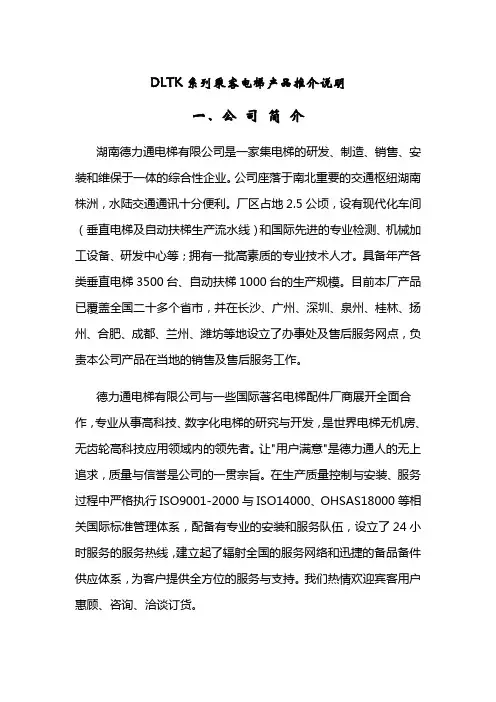
DLTK系列乘客电梯产品推介说明一、公司简介湖南德力通电梯有限公司是一家集电梯的研发、制造、销售、安装和维保于一体的综合性企业。
公司座落于南北重要的交通枢纽湖南株洲,水陆交通通讯十分便利。
厂区占地2.5公顷,设有现代化车间(垂直电梯及自动扶梯生产流水线)和国际先进的专业检测、机械加工设备、研发中心等;拥有一批高素质的专业技术人才。
具备年产各类垂直电梯3500台、自动扶梯1000台的生产规模。
目前本厂产品已覆盖全国二十多个省市,并在长沙、广州、深圳、泉州、桂林、扬州、合肥、成都、兰州、潍坊等地设立了办事处及售后服务网点,负责本公司产品在当地的销售及售后服务工作。
德力通电梯有限公司与一些国际著名电梯配件厂商展开全面合作,专业从事高科技、数字化电梯的研究与开发,是世界电梯无机房、无齿轮高科技应用领域内的领先者。
让"用户满意"是德力通人的无上追求,质量与信誉是公司的一贯宗旨。
在生产质量控制与安装、服务过程中严格执行ISO9001-2000与ISO14000、OHSAS18000等相关国际标准管理体系,配备有专业的安装和服务队伍,设立了24小时服务的服务热线,建立起了辐射全国的服务网络和迅捷的备品备件供应体系,为客户提供全方位的服务与支持。
我们热情欢迎宾客用户惠顾、咨询、洽谈订货。
二、产品介绍DLTK系列乘客电梯,是湖南德力通电梯有限公司推出的最新一代高科技绿色环保产品,它具有高效节能、低噪声、无(齿轮箱)油污染、无电源电网污染等优点。
一、最先进的永磁同步拖动系统DLTK系列乘客电梯,采用国际上最先进的永磁同步变频调速拖动技术。
永磁同步电机不需要无功励磁电流,定子铜耗小,功率因素高,并具有低速性、快速性、硬机械特性、停车自闭等优点。
同时,永磁同步电机正常工作时不产生谐波干扰,对电源电网无污染。
二、平稳高效的无齿轮曳引系统DLTK系列乘客电梯,采用无齿轮曳引技术,没有齿轮啮合,彻底消除了齿轮机械传动的振动和噪声,使电梯运行更加平稳,噪声大为降低。
目录目录 (I)摘要 (I)1.绪论 (1)2.课程设计主要内容及要求 (2)2.1设计内容 (2)2.2 基本要求 (2)3.方案设计与认证 (3)4.电路设计原理分析及仿真 (4)4.1设计原理 (4)4.2电路参考原理图 (5)4.3电路工作原理分析 (5)4.3.1 温度传感器 (5)4.3.2四路选择及控制部分 (8)4.3.3 A /D转换部分及显示部分 (8)5.电路的组装与调试 (11)5.1 电路的组装 (11)5.2 电路的调试 (11)6.设计心得 (13)7.参考文献 (14)摘要本文介绍了一种采用中规模集成模块进行设计的4路温度测控电路的设计方法,本次设计包含四大部分:温度信号检测及放大部分、数字控制部分、A/D转换部分及数字显示部分.本系统可以对四路温度进行巡回检测,其测量范围0℃~100℃,可用于工业生产、农业生产、粮仓温度测量等方面,具有实用性强、可靠性高、测量精度高等特点.关键词:温度信号检测;放大;数字控制;A/D转换;数字显示1.绪论电子技术课程设计是在《模拟电子技术基础》和《数字电子技术》的理论教学和实验教学基础上,进行的实践性教学环节。
其目的是使学生较系统掌握一般电子电路的设计方法。
提高学生综合分析问题和解决实际问题的能力,为学习后续课程和从事相关专业研究奠定基础。
本课程的基本知识教学目标与能力目标是:通过理论和实践教学,使学生了解四路温度检测电路的工作原理,特性参数及微变等效电路,掌握数字电子技术基础单元电路的线路组成、基本工作原理、分析方法、技术要求及一些典型集成电路的实际应用,并且具备一定的理论水平和足够的实践技能,以及使用先进仿真软件的能力,为进一步学习、掌握电子、通讯技术的专业知识和职业技能打下基础。
温度是表征物体冷热程度的物理量,本课程设计针对生产中常遇到的多路温度测控问题,提出以中规模集成模块为核心的4路温度测控仪表的设计方案,该系统设计还具有结构紧凑,测量精度高,抗干扰能力强.测温范围广。
高精度D/A转换芯片—TLV5616TLV5616 是12 位电压输出的4 线可变串行接口的数模转换器。
4 线串行接口无缝接入TMS320,SPI,QSPI 和Microwire 串行接口。
电源供电电压范围2.7V~5.5V。
LTV5616 采用16 位串行串编程,其中包含4位控制位和12 位的数据位.为了适合范围较宽的供电电压。
1.TLV5616的引脚图及其说明:电阻串输出电压被2×a 的增益的轨至轨输出缓冲器。
缓冲器能够提高一个AB 类的输出级的稳定性和减少结束的时间。
DAC 的结束时间是可编程的以此来允许设计者对比电源的损耗设计最佳的速度。
通过输入串行的16 位中的控制位来选择结束的时间。
高阻抗缓冲集成在REFIN 端来减少对低源阻抗驱动端口的需要。
2.TLV5616的功能模块图:3. TLV5616的接口图当REF 是参考电压CODE 是在0x000~0xFFF 范围内的数字输入值时,上电复位初始复位外部触发器到一个固定的状态(全为0)。
串行接口说明数据的转换:首先器件必须设置/CS 为低电平时器件有效,然后在FS 的下降边缘开始一位一位转移数据(开始是高位有效位)在SCLK 的下降边缘转移到内部寄存器。
在16 位都被转换后或FS 上升时,转移寄存器的内容移到DAC 的触发器使其输出电压更新到一个新的电平。
TLV5616 串行接口可以采用两个基本模式:. 四线(包括片选). 三线(不包括片选)使用片选(四线模式)使得多个器件连接到串行口的数据源(DSP 或微控制器)成为可能。
接口是TMS320 类兼容的,下图给出了2 个TLV 5616 直接连接到TMS320DSP 上的例子。
如果串行总线上只有一个器件,那么/CS 可以接低电平,16 给出了TLV5616 如何在SPI 或图Microwire 接口三线引脚下连接到一个TMS320 上的例子。
注意SPI 和Microwire:在控制器开始转换数据之前软件必须在FS 连接的I/O 引脚上产生一个下降缘。
液压支架电液控制器(SCU)PM4操作软件手册铁法第三套自动化刨煤机系统Version 版本: Tiefa III V 1.00SUPPORT CONTROL UNIT PM4 (SCU) 支架电液控制器PM4 (SCU) (6)E NCLOSURE D ESIGN 外壳设计 (6)K EYBOARD D ESIGN 键盘设计 (7)T IEFA III F OIL 铁法第三套键盘膜片 (7)E LECTRONIC C IRCUIT C ARD A SSEMBLY 组装电子功能卡 (7)E MERGENCY S TOP/L OCKOUT F EATURES 紧急停车/闭锁功能 (8)SOLENOID DRIVER MODULE (SDM) 螺纹驱动器(电磁阀)模块(SDM) (10)POWER SUPPLY WITH INTEGRATED POWER ADAPTER (PA)配备集成电源适配器(PA)的电源 (12)ISOLATION ADAPTER (IA) 绝缘适配器(IA) (13)SENSORS 传感器 (14)P RESSURE S ENSOR 压力传感器 (14)R EED C ONTACT A DVANCING R AM 推移千斤顶测控杆 (15)SKK 24 ELECTRICAL CABLE SYSTEM 电缆系统SKK 24 (16)VIEW TO PM 4 CONNECTION PORTS PM 4 连接端口视图 (18)VALVE CONNECTIONS 阀连接 (20)SYSTEM OVERVIEW DRAWING 系统全貌图 (21)F ACE S UPPORT C OMPONENTS 工作面支架部件I (21)F ACE S UPPORT C OMPONENTS 工作面支架部件II (22)F ACE E ND S UPPORT C OMPONENTS 工作面端头支架部件 (22)S YSTEM O VERVIEW 系统全貌I - VI (23)S YSTEM MCU2 MCU2 系统 (29)THE PM4 CONTROL PANEL PM4 控制面板 (30)PM4 KEYBOARD FUNCTIONS PM4 键盘功能 (31)DISPLAY 显示 (38)D EFAULT DISPLAY 缺省显示 (38)E MERGENCY S TOP I NDICATION 紧急停车显示 (38)L OCAL L OCKOUT I NDICATION 本架闭锁显示 (38)D ISPLAY OF D ISCONNECTED OR D AMAGED S ENSORS 显示未连接或损坏的传感器 (38)MENU OVERVIEW 菜单一览表 (39)THE MENU PLAN FOR THE TIEFA III PROGRAM 铁法第三套刨煤机PM4 菜单程序 (40)A UXILIARY F UNCTIONS 辅助功能 (41)Tiefa Third Automated Plow System铁法第三套自动化刨煤机系统PM4 Operating Software Manual PM4 操作软件手册Date 日期:2006-02Version 版本:4 CONTRACT 合同05-CTKX/2324126CDD EFAULT DISPLAY 缺省显示 (41)M EASURED V ALUES 测定的数据 (42)E RROR M ESSAGES 错误信息 (43)G LOBAL P ARAMETER 共用参数 (45)I NCREMENTAL P LOWING 固定刨深刨煤方式 (47)P ROHIBIT A CTIONS 禁止动作 (50)B LOCKANCHORAGE 分段锚固 (52)S ERVICE 服务 (54)A UTOSEQUENCE (ASQ, BATCH) P ARAMETER 自动排序(ASQ, BATCH) 参数 (57)B ANKPUSH P ARAMETERS 成组推移参数 (60)PRT P ULLBACK 拉回运行轨道 (62)C ONTROL P ARAMETER 控制参数 (63)E MERGENCY S TOP 紧急停车 (64)POSITIVE SET AUTOMATIC (PSA) 初撑力自动保持(PSA) (65)F UNCTION OF PSA 初撑力自动保持功能 (65)F UNCTION D IAGRAM PSA 初撑力自动保持功能图解 (66)PM4 OPERATION 操作PM4 (67)D IRECT A DJACENT C ONTROL F UNCTIONS 直接控制邻架功能 (67)R EMOTE A DJACENT C ONTROL F UNCTIONS 遥控邻架功能 (69)A UTOSEQUENCE (ASQ) 自动排序(ASQ) (71)N EIGHBOR F ATCH 邻架成组控制 (72)B ANKPUSH 成组推移 (74)PRT P ULLBACK 拉回运行轨道 (76)P ARAMETER C HANGES 改变参数 (77)INCREMENTAL PLOWING WITHOUT MCU 不使用主控台MCU 实现定距刨煤 (78)ACTIVATION OF PLOWING MODE CON, CONVENTIONAL PLOWING (78)THE SERVER-PM4 PM4 服务器 (79)T HE M ENU P LAN OF THE S ERVER-PM4 PM4 服务器菜单 (79)A UXILIARY F UNCTIONS 辅助功能 (80)S YSTEM S TATUS M ENUE 系统状况菜单 (80)S ERVICE M ENUE 服务菜单 (82)R UNNING THE I NCREMENTAL P LOWING ONLY BY THE S ERVER-PM4只靠PM4 服务器来运行定距刨煤 (84)M OVING OF S ERVER-PM4 TO S UPPORT N O. 1 把PM4 服务器移到第1 号支架 (85)INSTALLATION OF PM4 安装PM4 (86)INSTALL THE PM4 TO THE C ABLE B RACKET 把安装到黄铜电缆托架上 (86)L OAD THE S OFTWARE 下载软件 (86)Date 日期:2006-02 Version 版本:Tiefa III V 1.00DOC NO 文件号:ECN 4007 134 BA 00 5Safety instructions 安全指南Don’t activate support functions in areas where persons are staying !有人停留在支架时不要启动支架功能!The pushing of the red emergency-stop-button only stops all running electrical activated support actions !按下红色紧急停车按钮只能停止所有电气控制的支架动作!Mining equipment (plow-system) and prt not gets switched off !刨煤机系统和运行轨道不会停止!The pushing of the black fast stop buttons in supports without PM4 only stops all running electrical activated support actions !在不配备PM4 的支架按下黑色急停按钮只能停止所有电气控制的支架动作!Mining equipment (plow-system) and prt not gets switched off !刨煤机系统和运行轨道不会停止!While working or staying longer in a support secure yourself by pushing the black support-lock-switch of the PM4 at your actual position.如果在支架工作或停留时间较长,按下本架PM4 的黑色支架闭锁按钮!The PM4 display must show ‘>> locked <<‘ !PM4 显示屏幕必须显示出‘>> locked <<‘!Check the solenoid driver for the led´s are off or red !检查螺纹驱动器显示灯是否关闭或红色!While working on plow and PRT secure yourself by pushing the black support-lock-switch of PM4 at your actual position and in both neighbor PM4s ! 当对刨煤机和运行轨道进行工作时按下本架和两侧邻架PM4 的黑色支架闭锁按钮来保护自己!The PM4 display must show ‘>> locked <<‘ !PM4 显示屏幕必须显示出show ‘>> locked <<‘ !By running the full automatic mode during incremental plowing different automatic functions in front and behind the mowing plow are possible.采用全自动模式进行定距刨煤时,可以在运行中的刨头前后实现不同的自动功能。
The UCC5614 provides 9 lines of active termination for a SCSI (Small Computer Systems Interface) parallel bus. The SCSI standard recom-mends active termination at both ends of the cable.The UCC5614 is ideal for high performance 3.3V SCSI systems. The key features contributing to such low operating voltage are the 0.1V drop out regulator and the 2.7V reference. The reduced reference voltage was necessary to accommodate the lower termination current dictated in the SCSI-3 specification. During disconnect the supply current is typically only 0.5µA, which makes the IC attractive for battery powered systems.The UCC5614 is designed with an ultra low channel capacitance of 1.8pF , which eliminates effects on signal integrity from disconnected ter-minators at interim points on the bus.The UCC5614 can be programmed for either a 110 ohm or 2.5k ohm ter-mination. The 110 ohm termination is used for standard SCSI bus lengths and the 2.5k ohm termination is typically used in short bus applications.When driving the TTL compatible DISCNCT pin directly, the 110 ohm ter-mination is connected when the DISCNCT pin is driven low, and discon-nected when driven high. When the DISCNCT pin is driven through an impedance between 80k and 150k, the 2.5k ohm termination is con-nected when the DISCNCT pin is driven low, and disconnected when driven high.9-Line 3-5 Volt Low Capacitance SCSI Active TerminatorFEATURESDESCRIPTIONCircuit Design Patented•Complies with SCSI, SCSI-2 and SCSI-3 Standards • 2.7V to 7V Operation• 1.8pF Channel Capacitance during Disconnect•0.5µA Supply Current in Disconnect Mode•110 Ohm/2.5k Programmable Termination•Completely Meets SCSI Hot Plugging •-400mA Sourcing Current for Termination•+400mA Sinking Current for Active Negation Drivers•Trimmed Termination Current to 4%•Trimmed Impedance to 7%•Current Limit and Thermal Shutdown Protectioncontinued12/94The power amplifier output stage allows the UCC5614 to source full termination current and sink active negation current when all termination lines are actively negated. The UCC5614 is pin for pin compatible with Unitrode’s other 9 line SCSI terminators, allowing lower capacitance and lower voltage upgrades to existing systems. The UCC5614, as with all Unitrode terminators, is completely hot pluggable and appears as high impedance at the ter-minating channels with V TRMPWR = 0V or open.Internal circuit trimming is utilized, first to trim the 110 ohm termination impedance to a 7% tolerance, and then most importantly, to trim the output current to a 4% toler-ance, as close to the max SCSI-3 spec as possible, which maximizes noise margin in fast SCSI operation.Other features include thermal shutdown and current limit.This device is offered in low thermal resistance versions of the industry standard 16 pin narrow body SOIC, 16 pin ZIP (Zig-Zag In Line package), 24 pin TSSOP and 28 pin PLCC.ABSOLUTE MAXIMUM RATINGSTermpwr Voltage. . . . . . . . . . . . . . . . . . . . . . . . . . . . . . . . . +7V Signal Line Voltage. . . . . . . . . . . . . . . . . . . . . . . . . . . 0V to +7V Regulator Output Current. . . . . . . . . . . . . . . . . . . . . . . . . . 0.6A Storage Temperature. . . . . . . . . . . . . . . . . . . −65°C to +150°C Operating Temperature. . . . . . . . . . . . . . . . . −55°C to +150°C Lead Temperature (Soldering, 10 Sec.). . . . . . . . . . . . . +300°C RECOMMENDED OPERATING CONDITIONS Termpwr Voltage. . . . . . . . . . . . . . . . . . . . . . . . . 2.7V to 5.25V Signal Line Voltage. . . . . . . . . . . . . . . . . . . . . . . . . . . 0V to +5V Disconnect Input Voltage. . . . . . . . . . . . . . . . . . 0V to TermpwrDescription ContinuedUnless otherwise specified all voltages are with respect to Ground. Currents are positive into, negative out of the speci-fied terminal.Consult Packaging Section of Unitrode Integrated Circuits dat-abook for thermal limitations and considerations of packages.Note: Drawings are not to scale.Note: Drawings are not to scale.serve as heatsink/ground.17, 18, 19, and 20 serve as heatsink/ground.ELECTRICAL CHARACTERISTICS Unless otherwise stated, these specifications apply for T A = 0°C to 70°C.TRMPWR = 3.3V, DISCNCT = 0V, R DISCNCT = 0 ohms. T A = T J .ELECTRICAL CHARACTERISTICS (cont.) Unless otherwise stated, these specifications apply for T A = 0°C to 70°C.TRMPWR = 3.3V, DISCNCT = 0V, R DISCNCT = 0 ohms. T A = T J .Note 2:Guaranteed by design. Not 100% tested in production.Figure 1: Typical SCSI Bus Configurations Utilizing 2 UCC5614 DevicesFigure 2: Typical Wide SCSI Bus Configurations Utilizing 3 UCC5614 Devices.UNITRODE INTEGRATED CIRCUITS7 CONTINENTAL BLVD. • MERRIMACK, NH 03054TEL. (603) 424-2410 • FAX (603) 424-3460IMPORTANT NOTICETexas Instruments and its subsidiaries (TI) reserve the right to make changes to their products or to discontinue any product or service without notice, and advise customers to obtain the latest version of relevant information to verify, before placing orders, that information being relied on is current and complete. All products are sold subject to the terms and conditions of sale supplied at the time of order acknowledgement, including those pertaining to warranty, patent infringement, and limitation of liability.TI warrants performance of its semiconductor products to the specifications applicable at the time of sale in accordance with TI’s standard warranty. Testing and other quality control techniques are utilized to the extent TI deems necessary to support this warranty. Specific testing of all parameters of each device is not necessarily performed, except those mandated by government requirements.CERTAIN APPLICATIONS USING SEMICONDUCTOR PRODUCTS MAY INVOLVE POTENTIAL RISKS OF DEATH, PERSONAL INJURY, OR SEVERE PROPERTY OR ENVIRONMENTAL DAMAGE (“CRITICAL APPLICATIONS”). TI SEMICONDUCTOR PRODUCTS ARE NOT DESIGNED, AUTHORIZED, OR WARRANTED TO BE SUITABLE FOR USE IN LIFE-SUPPORT DEVICES OR SYSTEMS OR OTHER CRITICAL APPLICATIONS. INCLUSION OF TI PRODUCTS IN SUCH APPLICATIONS IS UNDERSTOOD TO BE FULLY AT THE CUSTOMER’S RISK.In order to minimize risks associated with the customer’s applications, adequate design and operating safeguards must be provided by the customer to minimize inherent or procedural hazards.TI assumes no liability for applications assistance or customer product design. TI does not warrant or represent that any license, either express or implied, is granted under any patent right, copyright, mask work right, or other intellectual property right of TI covering or relating to any combination, machine, or process in which such semiconductor products or services might be or are used. TI’s publication of information regarding any third party’s products or services does not constitute TI’s approval, warranty or endorsement thereof.Copyright © 1999, Texas Instruments Incorporated。
UCC561SLUS413B --MAY 1999--REVISED NOVEMBER 2002LOW-VOLTAGE DIFFERENTIAL SCSI (LVD)27-LINE REGULATORSETFEATURESD SCSI SPI--2,SPI--3and SPI--4LVD SCSI 27-Line,Low-Voltage Differential Regulator D 2.7-V to 5.25-V OperationDIntegrated Regulator Set for LVD SCSID Differential Failsafe Bias APPLICATIONS D ServersD Workstations D RAID BoxesDESCRIPTIONThe UCC561low-voltage differential (LVD)regulator set is designed to provide the correct references voltages and bias currents for LVD termination resistor networks (4759,1219,and 4759).The device also provides a 1.3-V output for “diff sense”signaling.With the proper resistor network,the UCC561solution meets the common mode bias impedance,differential bias,and termination impedance requirements of SPI--2(Ultra2),SPI--3(Ultra3/Ultra160)and SPI--4(Ultra320).The UCC561is not intended for SPI--5applications.This device incorporates into a single monolith,two sink/source reference voltage regulators,a 1.3-V buffered output and protection features.The protection features include thermal shutdown and active current-limiting circuitry.The UCC561is offered in 16-pin SOIC (DP)package.DIFSENSTRMPWRREG1REG2UDG--980932.7V TO 5.25VPRODUCTION DATA information is current as of publication date.Products conform to specifications per the terms of Texas Instruments standard warranty.Production processing does not necessarily include testing of allparameters.Please be aware that an important notice concerning availability,standard warranty,and use in critical applications of T exas Instruments semiconductor products and disclaimers thereto appears at the end of this data sheet.Copyright ã2002,Texas Instruments Incorporated元器件交易网UCC561SLUS413B --MAY 1999--REVISED NOVEMBER 20022This integrated circuit can be damaged by ESD.T exas Instruments recommends that all integrated circuits be handled with appropriateprecautions.Failure to observe proper handling and installation procedures can cause damage.ESD damage can range from subtle performance degradation to complete device failure.Precision integrated circuits may be more susceptible to damage because very small parametric changes could cause the device not to meet its published specifications.ORDERING INFORMATIONPRODUCT PACKAGE--LEADPACKAGE DESIGNATORSPECIFIED TEMPERATURERANGE ORDERING NUMBER TRANSPORT MEDIA,QUANTITYUCC561SOIC--16DP0°C to 70°CUCC561DPRail,70(1)For the most current specification and package information,refer to our web site at .ABSOLUTE MAXIMUM RATINGSover operating free-air temperature range unless otherwise noted (1)(2)UCC561UNIT TERMPWR 6V Package dissipation 1.2W Junction temperature,T J --55to 150°C Storage temperature,T stg--65to 150°C(1)Stresses beyond those listed under “absolute maximum ratings”may cause permanent damage to the device.These are stress ratings only,and functional operation of the device at these or any other conditions beyond those indicated under “recommended operating conditions”is not implied.Exposure to absolute-maximum-rated conditions for extended periods may affect device reliability.(2)Currents are positive into and negative out of the specified terminals.RECOMMENDED OPERATING CONDITIONSMINNOMMAX UNIT V TERMPWR ,T ermPowervoltage2.705.25VNCTERMPWRREG2HSPGND HSGND REG1DIFSENSNCNC NC NCHSGND HSGND NC NC NCDP PACKAGE (TOP VIEW)NC =No connection元器件交易网UCC561SLUS413B --MAY 1999--REVISED NOVEMBER 20023ELECTRICAL CHARACTERISTICST J =0°C to 70°C,V TERMPWR =3.3V unless otherwise noted (1)PARAMETERTEST CONDITIONSMINTYPMAX UNIT TERMPWR Supply Current TERMPWR supply current No load40mA TERMPWR voltage 2.705.25VRegulator 1.75-V regulator REG1(±125mA) 1.70 1.75 1.801.3-V regulator --5mA £I DIFSENS £50m A 1.2 1.3 1.40.75-V regulatorREG2(±125mA)0.700.750.80V 1.75-V regulator source current V O =1.25V --2001.75-V regulator sink currentV O =2.25V2001.75-V regulator source current limit (1)--200--7001.75-V regulator sink current limit (1)200700mA1.3-V regulator source current V DIFSENS =0V --5--151.3-V regulator sink current V DIFSENS =2.4V 50200m A 0.75-V regulator source current V O =0.25V --2000.75-V regulator sink currentV O =1.25V200A0.75-V regulator source current limit (1)--200--700mA 0.75-V regulator sink current limit (1)200700(1)Ensured by design.Not production tested.TERMINAL FUNCTIONSTERMINAL NAME NO .I/O DESCRIPTIONHSPGND 4--Heat sink power ground pin.HSGND 5,12,13--Heat sink ground pin which should be attached to the ground plane on a multilayer board or large cop-per area on a 2layer board.REG16O1.75-V source/sink regulated output voltage pin.The part is internally current limited for both sinkingand sourcing current to prevent damage.For best performance,a 4.7-m F low-ESR capacitor is recom-mended.Lead lengths should be kept to a minimum.REG23O 0.75-V source/sink regulated output voltage pin.The part is internally current limited for both sinking and sourcing current to prevent damage.For best performance,a 4.7-m F low-ESR capacitor is recom-mended.Lead lengths should be kept to a minimum.DIFSENS 7O 1.3-V source/sink regulated output voltage pin.The part is internally current limited to the SCSI SPI--2through SPI--4standards for both sinking and sourcing current to prevent damage.TERMPWR2ISupply voltage pin.The pin should be decoupled with at least a 2.2-m F low-ESR capacitor.For best performance,a 4.7-m F low--ESR capacitor is recommended.Lead lengths should be kept to a mini-mum.元器件交易网UCC561SLUS413B --MAY 1999--REVISED NOVEMBER 20024APPLICATION INFORMATIONThe resistor stack with the 1.75-V and 0.75-V reference gives the correct differential impedance,bias voltage,common mode differential impedance,and common mode voltage as show in Table 1.Table 1.UCC561Resistor Stack vs.Standard (SPI--2through SPI--4)PARAMETERUCC561STANDARD UNITS Differential Impedance 107.3100to 110W Differential bias voltage112.9100to 125mV Common-mode differential impedance 237100to 300W Common-mode voltage1.251.2to 1.3VUDG--98096L1+L27--L27+L1--DIFSENS2.7V Figure 1.Low-Voltage Differential Discrete Resistor Stack元器件交易网PACKAGING INFORMATIONOrderable DeviceStatus (1)Package Type Package DrawingPins Package Qty Eco Plan (2)Lead/Ball Finish MSL Peak Temp (3)UCC561DP ACTIVE SOIC D 1640Green (RoHS &no Sb/Br)CU NIPDAU Level-1-260C-UNLIM UCC561DPG4ACTIVE SOIC D 1640Green (RoHS &no Sb/Br)CU NIPDAU Level-1-260C-UNLIM UCC561DPTR ACTIVE SOIC D 162500Green (RoHS &no Sb/Br)CU NIPDAU Level-1-260C-UNLIM UCC561DPTRG4ACTIVE SOIC D 162500Green (RoHS &no Sb/Br)CU NIPDAU Level-1-260C-UNLIM UCC561TDOBSOLETETO-220KC5TBDCall TICall TI(1)The marketing status values are defined as follows:ACTIVE:Product device recommended for new designs.LIFEBUY:TI has announced that the device will be discontinued,and a lifetime-buy period is in effect.NRND:Not recommended for new designs.Device is in production to support existing customers,but TI does not recommend using this part in a new design.PREVIEW:Device has been announced but is not in production.Samples may or may not be available.OBSOLETE:TI has discontinued the production of the device.(2)Eco Plan -The planned eco-friendly classification:Pb-Free (RoHS)or Green (RoHS &no Sb/Br)-please check /productcontent for the latest availability information and additional product content details.TBD:The Pb-Free/Green conversion plan has not been defined.Pb-Free (RoHS):TI's terms "Lead-Free"or "Pb-Free"mean semiconductor products that are compatible with the current RoHS requirements for all 6substances,including the requirement that lead not exceed 0.1%by weight in homogeneous materials.Where designed to be soldered at high temperatures,TI Pb-Free products are suitable for use in specified lead-free processes.Green (RoHS &no Sb/Br):TI defines "Green"to mean Pb-Free (RoHS compatible),and free of Bromine (Br)and Antimony (Sb)based flame retardants (Br or Sb do not exceed 0.1%by weight in homogeneous material)(3)MSL,Peak Temp.--The Moisture Sensitivity Level rating according to the JEDEC industry standard classifications,and peak solder temperature.Important Information and Disclaimer:The information provided on this pagerepresents TI's knowledge and belief as of the date that it is provided.TI bases its knowledge and belief on information provided by third parties,and makes no representation or warranty as to the accuracy of such information.Efforts are underway to better integrate information from third parties.TI has taken and continues to take reasonable steps to provide representative and accurate information but may not have conducted destructive testing or chemical analysis on incoming materials and chemicals.TI and TI suppliers consider certain information to be proprietary,and thus CAS numbers and other limited information may not be available for release.In no event shall TI's liability arising out of such information exceed the total purchase price of the TI part(s)at issue in this document sold by TI to Customer on an annual basis.PACKAGE OPTION ADDENDUM4-Nov-2005Addendum-Page 1元器件交易网IMPORTANT NOTICETexas Instruments Incorporated and its subsidiaries (TI) reserve the right to make corrections, modifications,enhancements, improvements, and other changes to its products and services at any time and to discontinueany product or service without notice. Customers should obtain the latest relevant information before placingorders and should verify that such information is current and complete. All products are sold subject to TI’s termsand conditions of sale supplied at the time of order acknowledgment.TI warrants performance of its hardware products to the specifications applicable at the time of sale inaccordance with TI’s standard warranty. T esting and other quality control techniques are used to the extent TIdeems necessary to support this warranty. Except where mandated by government requirements, testing of allparameters of each product is not necessarily performed.TI assumes no liability for applications assistance or customer product design. Customers are responsible fortheir products and applications using TI components. T o minimize the risks associated with customer productsand applications, customers should provide adequate design and operating safeguards.TI does not warrant or represent that any license, either express or implied, is granted under any TI patent right,copyright, mask work right, or other TI intellectual property right relating to any combination, machine, or processin which TI products or services are used. Information published by TI regarding third-party products or servicesdoes not constitute a license from TI to use such products or services or a warranty or endorsement thereof.Use of such information may require a license from a third party under the patents or other intellectual propertyof the third party, or a license from TI under the patents or other intellectual property of TI.Reproduction of information in TI data books or data sheets is permissible only if reproduction is withoutalteration and is accompanied by all associated warranties, conditions, limitations, and notices. Reproductionof this information with alteration is an unfair and deceptive business practice. TI is not responsible or liable forsuch altered documentation.Resale of TI products or services with statements different from or beyond the parameters stated by TI for thatproduct or service voids all express and any implied warranties for the associated TI product or service andis an unfair and deceptive business practice. TI is not responsible or liable for any such statements.Following are URLs where you can obtain information on other Texas Instruments products and applicationsolutions:Products ApplicationsAmplifiers Audio /audioData Converters Automotive /automotiveDSP Broadband /broadbandInterface Digital Control /digitalcontrolLogic Military /militaryPower Mgmt Optical Networking /opticalnetworkMicrocontrollers Security /securityTelephony /telephonyVideo & Imaging /videoWireless /wirelessMailing Address:Texas InstrumentsPost Office Box 655303 Dallas, Texas 75265Copyright 2005, Texas Instruments Incorporated。