EM644FV16FU中文资料
- 格式:pdf
- 大小:195.52 KB
- 文档页数:11


Document Title256K x16 bit Super Low Power and Low Voltage Full CMOS Static RAMRevision HistoryRevision No. History Draft Date Remark0.0Initial Draft May 26 , 2003 Preliminary0.12’nd Draft Add Pb-free part number February 13 , 2004Emerging Memory & Logic Solutions Inc.IT Venture Tower Eastside 11F, 78, Karac-Dong, Songpa-Ku, Seoul, Rep.of Korea Zip Code : 138-160Tel : +82-2-2142-1759~1766 Fax : +82-2-2142-1769 / Homepage : The attached datasheets are provided by EMLSI reserve the right to change the specifications and products. EMLSI will answer to your questions about device. If you have any questions, please contact the EMLSI office.FEATURES•Process Technology : 0.18µm Full CMOS •Organization : 256K x 16 bit•Power Supply Voltage : 2.7V ~ 3.6V •Low Data Retention Voltage : 1.5V(Min.)•Three state output and TTL Compatible •Package Type : 44-TSOP2GENERAL DESCRIPTIONThe EM643FV16FU families are fabricated by EMLSI’s advanced full CMOS process technology. The families support industrial temperature range and Chip Scale Package for user flexibility of system design. The fami-lies also supports low data retention voltage for battery back-up operation with low data retention current.PRODUCT FAMILYProduct FamilyOperating TemperatureVcc Range SpeedPower DissipationPKG TypeStandby (I SB1, Typ.) Operating (I CC1.Max.) EM643FV16FU Industrial (-40 ~ 85o C)2.7V~3.6V551) /70ns1 µA 2)3 mA44-TSOP2Name FunctionName FunctionCS Chip select input Vcc Power Supply O E Output Enable input Vss GroundWE Write Enable input UB Upper Byte (I/O 9~16)A 0~A 17Address InputsLBLower Byte (I/O 1~8)I/O 1~I/O 16 Data Inputs/outputsNC No ConnectionR o w S e l e c tI/O Circuit Column SelectData Cont Data ContPre-charge CircuitMemory Array 2048 x 2048A 1A 2A 3A 4A 5A 6A 7A 0A 8A 9A 11A 12A 13A 14A 15A 16A 17W EO E U BLB C SI/O1 ~ I/O8I/O9 ~ I/O16V C CV SSControl LogicFUNCTIONAL BLOCK DIAGRAM1. The parameter is measured with 30pF test load.A 10PIN DESCRIPTION 1234567891011121314151644434241403938373635343332313029A4A3A2A1A0C S I/O1I/O2I/O3I/O4VCC VSS I/O5I/O6I/O7I/O8A5A6A7OE UB LB I/O16I/O15I/O14I/O13VSS V C C I/O12I/O11I/O10I/O944 - TSOP2171819202122282726252423WE A17A16A15A14A13NC A8A9A10A11A122. Typical values are measured at Vcc=3.3V, T A =25o C and not 100% tested.ABSOLUTE MAXIMUM RATINGS *Parameter Symbol Ratings Unit Voltage on Any Pin Relative to Vss V IN, V OUT-0.2 to Vcc+0.3(Max.4.0V)V Voltage on Vcc supply relative to Vss V CC-0.2 to 4.0V V Power Dissipation P D 1.0W Operating Temperature T A-40 to 85o C*Stresses greater than those listed under “Absolute Maximum Ratings” may cause permanent damage to the device. Functional operation should be restricted to recommended operating condition. Exposure to absolute maximum rating conditions for extended periods may affect reliability.FUNCTIONAL DESCRIPTIONCS OE WE LB UB I/O1-8I/O9-16Mode PowerH X X X X High-Z High-Z Deselected Stand byL H H X X High-Z High-Z Output Disabled ActiveL X X H H High-Z High-Z Output Disabled ActiveL L H L H Data Out High-Z Lower Byte Read ActiveL L H H L High-Z Data Out Upper Byte Read ActiveL L H L L Data Out Data Out Word Read ActiveL X L L H Data In High-Z Lower Byte Write ActiveL X L H L High-Z Data In Upper Byte Write ActiveL X L L L Data in Data In Word Write ActiveNote: X means don’t care. (Must be low or high state)DC AND OPERATING CHARACTERISTICSNOTES1. Typical values are measured at Vcc=3.3V, T A =25o C and not 100% tested.ParameterSymbol Test Conditions Min Typ Max Unit Input leakage current I LI V IN =V SS to V CC-1-1µA Output leakage current I LO CS=V IH or OE=V IH or WE=V IL , V IO =V SS to V CC -1-1µA Operating power supplyI CC I IO =0mA, CS=V IL , V IN =V IH or V IL --3mA Average operating currentI CC1Cycle time=1µs, 100% duty, I IO =0mA, CS<0.2V, V IN <0.2V or V IN >V CC -0.2V --3mAI CC2Cycle time = Min, I IO =0mA, 100% duty, CS=V IL, V IN =V IL or V IH 55ns --30mA 70ns--25 Output low voltage V OL I OL = 2.1mA --0.4V Output high voltage V OH I OH = -1.0mA2.4--V Standby Current (TTL)I SB CS=V IH , Other inputs=V IH or V IL --0.3mAStandby Current (CMOS)I SB1CS>V CC -0.2V, Other inputs=0~V CC(Typ. condition : V CC =3.3V @ 25o C)(Max. condition : V CC =3.6V @ 85o C)LL LF-11)12µARECOMMENDED DC OPERATING CONDITIONS 1)1. TA= -40 to 85o C, otherwise specified2. Overshoot: V CC +2.0 V in case of pulse width < 20ns3. Undershoot: -2.0 V in case of pulse width < 20ns4. Overshoot and undershoot are sampled, not 100% tested .ParameterSymbol Min Typ Max Unit Supply voltage V CC 2.7 3.3 3.6V GroundV SS 000V Input high voltage V IH 2.2-V CC + 0.22)V Input low voltageV IL-0.23)-0.6VCAPACITANCE 1) (f =1MHz, T A =25o C)1. Capacitance is sampled, not 100% testedItemSymbol Test ConditionMin Max Unit Input capacitance C IN V IN =0V -8pF Input/Ouput capacitanceC IOV IO =0V-10pFEM643FV16FU SeriesLow Power, 256Kx16 SRAMmerging Memory & Logic Solutions Inc.ParameterSymbol55ns 70nsUnitMin Max Min Max Read cycle time t RC 55-70-ns Address access time t AA -55-70ns Chip select to outputt CO -55-70ns Output enable to valid output t OE -25-35ns UB, LB acess time t BA 25 35ns Chip select to low-Z output t LZ 10-10-ns UB, LB enable to low-Z output t BLZ 5- 5 -ns Output enable to low-Z output t OLZ 5-5-ns Chip disable to high-Z output t HZ 020025ns UB, LB disable to high-Z output t BHZ 020025ns Output disable to high-Z output t OHZ 020025ns Output hold from address changet OH10-10-nsParameterSymbol55ns 70nsUnitMin Max Min Max Write cycle timet WC 55-70-ns Chip select to end of write t CW 45-60-ns Address setup timet AS 0-0-ns Address valid to end of write t AW 45-60-ns UB, LB valid to end of write t BW 45-60-ns Write pulse width t WP 40-55-ns Write recovery time t WR 0-0-ns Write to ouput high-Z t WHZ 020025ns Data to write time overlap t DW 25 30 ns Data hold from write time t DH 0-0-ns End write to output low-Zt OW5-5-nsREAD CYCLE (V cc =2.7 to 3.6V, Gnd = 0V, T A = -40o C to +85o C)WRITE CYCLE (V cc =2.7 to 3.6V, Gnd = 0V, T A = -40o C to +85o C)AC OPERATING CONDITIONSTest Conditions (Test Load and Test Input/Output Reference)Input Pulse Level : 0.4 to 2.2V Input Rise and Fall Time : 5nsInput and Output reference Voltage : 1.5V Output Load (See right) : CL = 100pF+ 1 TTL CL 1) = 30pF + 1 TTL 1. Including scope and Jig capacitance 2. R 1=3070Ω, R 2=3150Ω3. V TM =2.8VCL 1)V TM 3)R 12)R 22)t AddressCSUB,LBOEData Outt COt OHt B At O EHigh-ZTIMING WAVEFORM OF READ CYCLE(2) (WE = V IH )Data ValidOLZt t LZAAHZt RCAddresst AA Data Validt OHPrevious Data ValidTIMING WAVEFORM OF READ CYCLE(1). IL IH, or/and =V IL )Data OutTIMING DIAGRAMSNOTES (READ CYCLE)1. t HZ and t OHZ are defined as the outputs achieve the open circuit conditions and are not referanced to output voltage levels.2. At any given temperature and voltage condition, t HZ (Max.) is less than t LZ (Min.) both for a given device and from device to device interconnection.WR (4)t WC AddressCS UB,LB WE Data in Data outt CW(2)t AWt BWt WP(1)t AS(3)High-Zt DW t DHHigh-Zt OWt WHZData UndefinedTIMING WAVEFORM OF WRITE CYCLE(1) (WE CONTROLLED)Data Validt WCAddressCS UB,LB WE Data in Data outt CW(2)t WR(4)t AWt BWt WP(1)t DW t DHTIMING WAVEFORM OF WRITE CYCLE(2) (CS CONTROLLED)tAS(3)High-Z High-ZData Validt AddressCSUB,LBWEData in Data outt CW (2)W R (4)t A W t B Wt W P (1)t DWDHTIMING WAVEFORM OF WRITE CYCLE(3) (UB, LB CONTROLLED)High-ZHigh-ZData ValidA S NOTES (WRITE CYCLE)1. A write occurs during the overlap(t WP ) of low CS and low WE. A write begins when CS goes low and WE goes low with asserting UB or LB for single byte operation or simultaneously asserting UB and LB for double byte operation. A write ends at the earliest transition when CS goes high and WE goes high. The t WP is measured from the beginning of write to the end of write.2. t CW is measured from the CS going low to end of write.3. t AS is measured from the address valid to the beginning of write.4. t WR is measured from the end or write to the address change. t WR applied in case a write ends as CS or WE going high.DATA RETENTION CHARACTERISTICSNOTES 1. See the I SB1 measurement condition of datasheet page 4.2. Typical values are measured at T A =25o C and not 100% tested.ParameterSymbolTest ConditionMinTyp 2)MaxUnitV CC for Data Retention V DR I SB1 Test Condition (Chip Disabled) 1)1.5- 3.6V Data Retention CurrentI DR V CC =1.5V, I SB1 Test Condition(Chip Disabled) 1)-0.5-µAChip Deselect to Data Retention Time t SDR See data retention wave form0--nsOperation Recovery Time t RDRt RC--V cc 2.7V2.2V V DRCS GNDDATA RETENTION WAVE FORMUnit: millimeters PACKAGE DIMENSIONEM643FV16FU SeriesLow Power, 256Kx16 SRAMmerging Memory & Logic Solutions Inc.1. EMLSI Memory2. Device Type3. Density 5. Technology 8. Version 9. Packages 10. Speed7. Orgainzation1. Memory Component2. Device Type6 ------------------------ Low Power SRAM7 ------------------------ STRAM 3. Density1 ------------------------- 1M2 ------------------------- 2M 4 ------------------------- 4M 8 ------------------------- 8M 16 ----------------------- 16M 32 ----------------------- 32M 64 ----------------------- 64M4. Mode Option 0 -------- Dual CS 1 -------- Single CS2 -------- Multiplexed Address3 -------- Single CS with LB,UB (tBA=tOE)4 -------- Single CS with LB,UB (tBA=tCO)5 -------- Dual CS with LB,UB (tBA=tOE)6 -------- Dual CS with LB,UB (tBA=tCO)5. TechnologyBlank ------------------ CMOSF ------------------------ Full CMOS 6. Operating Voltage Blank ------------------- 5VV ------------------------- 2.7V~3.6V U ------------------------- 3.0V S ------------------------- 2.5V R ------------------------- 2.0V P ------------------------- 1.8V4. Option 11. Power 7. Orginzation8 ---------------------- x8 bit 16 ---------------------- x16 bit 32 ---------------------- x32 bit8. VersionBlank ----------------- Mother Die A ----------------------- First revision B ----------------------- Second revision C ----------------------- Third revision D ----------------------- Fourth revision E ----------------------- Fifth revision F ----------------------- Sixth revision 9. PackageBlank ---------------------- FPBGAS ---------------------------- 32 sTSOP1 T ---------------------------- 32 TSOP1 U ---------------------------- 44 TSOP2 W ---------------------------- Wafer10. Speed45 ---------------------- 45ns 55 ---------------------- 55ns 70 ---------------------- 70ns 85 ---------------------- 85ns 10 --------------------- 100ns 12 --------------------- 120ns11. PowerLL ---------------------- Low Low PowerLF ---------------------- Low Low Power (Pb-free) L ---------------------- Low PowerS ---------------------- Standard Power元器件交易网。

Thank you for purchasing the Cineroid EVF.The Cineroid EVF (hereafter referred to as “EVF") is a view finder that can be mounted on any video camera with a HDMI output signal. Please thoroughly read the user manual for best operation and understanding of all of the functions of the EVF.Test Before OperatingIt is recommended to test the EVF before operating. Check if the EVF can be turned on once powered, and check if the information/menu is being properly displayed on the LCD.Copyrights and ProhibitionsThe use of images of people, property, and places can without permission can be prohibited by law. Please refer to your region’s laws regarding copyrights.02○ Canon and EOS are registered trademarks of Canon.○ Nikon is a registered trademark of Nikon.○ Sony is a registered trademark of Sony.○ Panasonic is a registered trademark of Panasonic.1. Do not face the eyecup directly into the sun as it may damage the LCD.2. The shadow disk is installed on EVF at factory. This shadow disk can be removed by disassembling eyecup from loupe.EnglishSafety Precautions◎ Do not use any batteries, power cord, or accessories that are not specified in this document.◎ When using a power cord, be sure to plug it in completely. Do not handle power plugswhen your hands are wet. When unplugging the power cord, grasp the plug body or adapter instead of the cord.◎ Power cords that are scratched, heavily bent or twisted can potentially be hazardous and a source of electric shock and/or fire.◎ Do not insert foreign objects into the product’s electric or cable components.◎ Do not place the power cord near sources of heat as this may melt or cause damage to the cord potentially causing fire or electric shock.◎ Do not disassemble or modify the product. This may damage the product and cause danger due to a malfunction.◎ Please keep the product out of reach of young children. Injuries may occur due to damage to the product.◎ When using the product in an airplane or hospital setting, it is recommended to acquireauthorization first as signals or electro-magnetic waves from the product may cause other equipment to malfunction.◎ Do not store the product in a dusty or humid environment as damage may occur.◎ When the product is mounted on a camera, do not lift or move the camera by grabbing the product. This may cause damage to the product or the camera mount.◎ Do not clean the product with paint thinner, benzene, or other volatile solvents. This may cause damage to the product and become a fire hazard.◎ This product is not waterproof. If the product is dropped in water, contact the servicecenter immediately.Please observe the following safety precautions as they are meant for the safe and proper use of the product to reduce the risk of accidents. Upon reading the user manual, keep it in a safe and available place.03Table of ContentsSafety PrecautionsTable of ContentsComponentsPartsBefore Using the EVFOpenable Optical LoupeHood for LoupeSeparate of LoupeAdjusting the Diopter / Connecting Extention Tube Installing the BatteryConnecting External PowerConnecting input / outputPower On/OffBasic FeaturesOperating the MenuAdjusting ColorAdjusting the ScreenVolume Control 03 04 06 07 08 08 09 09 10 10 11 1112 13 13 1304EnglishShooting Features Peaking Pixel to Pixel Clip guideWaveform / Vectorscope False color 1 False color 2 Monochrome Look up table FreezeOver Scaling Underscan Crop Guide Anamorphic Center Marker Time Code Screen FlipSetting User Controls Custom Button Functions Firmware UpgradeCustom Display Settings Parameter Save And Restore Factory ResetProduct Specifications Optional Products051415151617172020212518212323251919242418222224ComponentsPlease ensure all parts are present after opening the box.06EnglishParts 0708Openable Optical LoupeHood for LoupeThe optical loupe attached to the EVF body can beflipped open 180 degrees.English09Separate of Loupecompletely.When viewing through the optical loupe, the user can adjust the diopter accordingly. Rotate the dial in either direction until the image becomes clear. and Extention tube is used toextend loupe length for old eye.Adjusting the Diopter / Connecting Extension tube1 Touch Removealbe10Connecting External PowerDC in 6~17VProper voltage for external power is 6-17V.Attention to the connecting polarities and voltage, otherwise the connectors may be damaged.When both external power and battery is connected, battery is not consumed.Before Using the EVF Connecting input / outputOperating the Menu3. to access that feature.EnglishPeakingOn/Off : Menu - Control1 - Peaking Setting : Menu - Setting1 - PeakingPeaking Red ONPeaking Red OFF Peaking On / OffPeaking SettingTo activate the peaking feature, simply press the F1 button on the left side of theEVF body. The peaking will show in the mode that is currently selected.Simple Peaking Button*Peaking Sharpness OFF Peaking Sharpness ONEnglishPixel to pixelOn/Off : Menu - Control1 - Pixel to PixelPixel to Pixel Off Pixel to Pixel OnPixel to Pixel Off Clip GuideOn/Off : Menu - Control1 - Clip Guide Setting : Menu - Setting1 - Clip GuideClip Guide Off Clip Guide Color mode Clip Guide Zebra modeClip Guide On / Off Clip Guide SettingPixel to Pixel OnWaveform / VectorscopeOn/Off : Menu - Control1 - Waveform Setting : Menu - Setting1 - WaveformStyle 1. Only horizontal waveform withimage croppingWaveform OFFStyle 2. Horizontal and vertical waveform with small vectorscope Style 3. Horizontal and vertical waveform with big vectorscopeWaveform On / OffWaveform Setting T o c h a n g e t h e w a v e f o r m s t y l e,s i m p l y s c r o l lthe wheel button on the left side of the cineroidE V F4R V W's b o d y.T h e w a v e f o r m s t y l e w i l ls h o w i n t h e m o d e t h a t i s c u r r e n t l y s e l e c t e d.Simple change waveform style*False Color2 Off False Color2 OnLook up tableOn/Off : Menu - Control1 - Look up tableLook up table Off(The image applied adjusting color)Look up table OffLook up table On(Original image)Monochrome (B /W, Blue, Red, Green)On/Off : Menu - Control1 - Monochrome Setting : Menu - Setting1 - MonochromeMonochrome On / Off Monochrome SettingMonochrome (B/W) OffMonochrome (B/W) OnFreezeOn/Off : Menu - Control1 - FreezeEnglish Freeze Off Freeze OnFreeze Off Freeze OnCrop guideOn/Off : Menu - Control2 - Crop Guide Setting : Menu - Setting1 - Crop GuideCrop guide Off Crop guide OnCrop guide On / Off Crop guide SettingUnderscanOn/Off : Menu - Control2 - UnderscanUnderscan Off Underscan OnUnderscan Off Underscan OnEnglish21Shooting FeaturesCenter MarkerOn/Off : Menu - Control2 - Center MarkerCenter Marker Off Center Marker Off Center Marker OnCenter Marker OnAnamorphicOn/Off : Menu - Control2 - Anamorphic Setting : Menu - Setting1 - AnamorphicAnamorphic Off Anamorphic OnAnamorphic On / Off Anamorphic SettingTime CodeOn/Off : Menu - Control2 - Time CodeTime code Off Time Code OnTime Code On / Off Time Code Setting22TC 01:22:34EnglishCustom Button FunctionsSetting : Menu - Setting2 - Key AllocationThe left side of the EVF body contains the buttons F1, F2, F3, F4. The factory default forFirmware Upgrade1. Firmware is upgradable by special cable.2. Connect EVF and computer by cable.3. Select On of Firmware Upgrade. The screen is changed to waiting message.4. EVF starts firmware upgrade.Setting User ControlsControl1 Control2 Setting1 Setting2 System ExitF1-Back / Exit Firmware Upgrade set V01.03Input Select Parameter Save Parameter Restore Firmware Exit Upgrade Cancel23Setting User ControlsCustom Display SettingsSetting : Menu - Setting1 - AnamorphicYou can select to view the current state of the battery usage, volume, etc. on the LCD.Factory reset1. Powering on the EVF while pressing down the F1 button will reset the EVF to its original default settings.2. Once the reset is complete, fully power off the EVF before powering on for further use.Parameter save and restoreSetting : Menu - System - Parameter Save/RestoreThe all parameters of function can be stored on bank0 or bank1. The parameters can be restored from bank0 or bank1. Factory is the initial parameter of factory.Parameter Save Parameter Restore24Peaking ONOSD Pixel to Pixel ONEnglishProduct Specifications25Optional Product2627Seculine Co., LTD.Tel +82.70.4347.4901 / Fax +82.2.850.3027Rm.510, Kolon Science Valley #2, Guro-dong, 811, Guro-gu, Seoul, 152-728, Korea Homepage E-mail *******************Printed in KoreaEVF1.0We will strive to create the best products andprovide superb service.。

MICRO SWITCH Miniature Toggle SwitchesMT SeriesDESCRIPTIONHoneywell MICRO SWITCH MT Series miniature toggle switches are designed to meet the need for a rugged, cost-effective toggle switch. Quality construction features include a seal between the toggle lever and bushing, and between the cover and case. These switches are designed for use inapplications in many demanding outdoor environments, where the panels are subjected to such things as vibration fromequipment, temperature extremes, dust, splashing water, and/or hose directed water.They are capable of withstanding exposure to heavyaccumulations of early morning dew that may condense on the control panel in cabs of vehicles left outdoors overnight. The MT toggle switches with metal or plastic levers are well suited for gloved-hand operation.The panel stand-off with O-ring feature available on some listings eliminates the need for behind-the-panel hardware, provides a uniform panel height, and a panel-to-cover seal.VALUE TO CUSTOMERS• Spring-loaded mechanism provides enhanced tactile feedback for toggle switch lever• High sealing level and electrical life cycle enable more uptime in field installations which helps in keeping machines working longer with less downtime• Small size allows for smaller control box/panel size to reduce weight and operator fatigueFEATURES• Miniature behind-panel size (case) enables overall control box or panel use• IEC 60529-2001, IP67, IP68 (except terminal parts) sealing for harsh-duty applications• Up to 60,000 electrical life that enhances the use time • Available with 8 circuitry options• 2- or 3- position maintained and momentary action to meet circuit and actuator requirements• UL recognized, CE certified for global usePOTENTIAL APPLICATIONSRemote control box of • Concrete pumping • Cranes• Material handling • Boom trucks• Any application with small panel constraintsDIFFERENTIATION• 60K life cycle offers an enhanced application life, keeping maintenance, replacement, and refurbishment at a minimum• High seal rating (IP68) to protect the toggle from water ingress and support more equipment uptimePORTFOLIOHoneywell offers an extensive line of MICRO SWITCH toggle switches, including the following Series: TL , NT , TW , TS , AT , and ET .Sensing and Internet of Things005437Issue 12 * These positions are momentary. All others are maintained.Sensing and Internet of Things 34 Figure 1. DImensions mm [in]2-Pole Switch7,291-Pole SwitchFigure 2. Panel CutoutPanel Cut-out005437-1-EN IL50 GLO December 2016© 2016 Honeywell International Inc. All rights reserved.m WARNINGPERSONAL INJURYDO NOT USE these products as safety or emergency stop devices or in any other application where failure of the product could result in personal injury.Failure to comply with these instructions could result in death or serious injury.m WARNINGMISUSE OF DOCUMENTATION• The information presented in this product sheet is for reference only. Do not use this document as a product installation guide.•Complete installation, operation, and maintenanceinformation is provided in the instructions supplied with each product.Failure to comply with these instructions could result in death or serious injury.Find out moreHoneywell serves its customers through a worldwide network of sales offices, representatives and distributors. For application as-sistance, current specifications, pricing or name of the nearest Authorized Distributor, contact your local sales office.To learn more about Honeywell’s sensing and switching products, call +1-815-235-6847 or 1-800-537-6945,visit , or e-mail inquiries to *********************ADDITIONAL MATERIALSThe following associated literature is available on the Honeywell web site at :• Product installation instructions • Product range guide• Product application-specific informationHoneywell Sensing and Internet of Things 9680 Old Bailes Road Fort Mill, SC 29707 Warranty/RemedyHoneywell warrants goods of its manufacture as being free of defective materials and faulty workmanship during the appli-cable warranty period. Honeywell’s standard product warranty applies unless agreed to otherwise by Honeywell in writing; please refer to your order acknowledgement or consult your local sales office for specific warranty details. If warrantedgoods are returned to Honeywell during the period of coverage, Honeywell will repair or replace, at its option, without charge those items that Honeywell, in its sole discretion, finds defec-tive. The foregoing is buyer’s sole remedy and is in lieu of all other warranties, expressed or implied, including those of merchantability and fitness for a particular purpose. In no event shall Honeywell be liable for consequential, special, or indirect damages.While Honeywell may provide application assistance personally, through our literature and the Honeywell web site, it is buyer’s sole responsibility to determine the suitability of the product in the application.Specifications may change without notice. The information we supply is believed to be accurate and reliable as of this writing. However, Honeywell assumes no responsibility for its use.。

Document Title256K x16 bit Super Low Power and Low Voltage Full CMOS Static RAMRevision HistoryRevision No. History Date Remark0.0-.Initial Draft May262003Preliminary0.1-.Add Pb-free part number Feb.1320040.2-.I SB1(Max.) changed from 12uA to 6uA.Mar.3120080.3-.Add 45ns part specification.Apr.22009-.I SB1(Typ.) changed from 1uA to 0.25uA.-.I SB1(Max.) changed from 6uA to 4uA.-.Memory Function Guide updated in the last page.Apr.72009Release1.0-.EM643FV16F(KGD), EM643FV16F series & EM643FV16FUseries are unified to EM643FV16F Family.Emerging Memory & Logic Solutions Inc.3F Korea Construction Financial Cooperative B/D, 301-1 Yeon-Dong, Jeju-Si, Jeju-Do, Rep.of Korea Zip Code : 690-717Tel : +82-64-740-1700 Fax : +82-64-740-1750 / Homepage : The attached datasheets are provided by EMLSI reserve the right to change the specifications and products. EMLSI will answer to your questions about device. If you have any questions, please contact the EMLSI office.PRODUCT FAMILY1. “xx” represents speed.2. Typical values are measured at Vcc=3.3V, T A =25o C and not 100% tested.Product FamilyOperating Temperature Vcc RangeSpeedPower DissipationPKG Type Standby (I SB1, Typ.)Operating (I CC1.Max.)EM643FV16F Industrial (-40 ~ 85o C)2.7 ~3.6 V 45/55/70 ns0.25 µA 2)3 mAKGDEM643FV16F - xx 1)LF VFBGA-48 EM643FV16FU - xx 1)LF44-TSOP2FEATURES•Process Technology : 0.18µm Full CMOS •Organization : 256K x 16 bit•Power Supply Voltage : 2.7V ~ 3.6V •Low Data Retention Voltage : 1.5V(Min.)•Three state output and TTL Compatible •Package Type : VFBGA-48, 44-TSOP2GENERAL DESCRIPTIONThe EM643FV16F families are fabricated by EMLSI’s advanced full CMOS process technology. The families support industrial temperature range and Chip Scale Package for user flexibility of system design. The families also supports low data retention voltage for battery back-up operation with low data retention current.R o w S e l e c tI/O Circuit Column SelectData ContData ContPre-charge CircuitMemory Array 2048 x 2048A1A2A3A4A5A6A7A0A8A9A11A12A13A14A15A16A17WE OE UB LB CSDQ0 ~ DQ7DQ8 ~ DQ15VCCVSSControl LogicA10FUNCTIONAL BLOCK DIAGRAMPIN DESCRIPTIONName FunctionName FunctionCS Chip Select input VCC Power Supply OE Output Enable input VSS GroundWE Write Enable input UB Upper Byte (DQ8~DQ15)A0~A17 Address inputs LB Lower Byte (DQ0~DQ7)DQ0~DQ15Data inputs/outputsNCNo ConnectionPIN CONFIGURATIONSVFBGA-48 : Top view(ball down)123456A LB OE A0A1A2NC B DQ8UB A3A4CS DQ0C DQ9DQ10A5A6DQ1DQ2D VSS DQ11A17A7DQ3VCCE VCC DQ12 NC A16DQ4VSSF DQ14DQ13A14A15DQ5DQ6G DQ15NC A12A13WE DQ7HNCA8A9A10A11NC1234567891011121314151644434241403938373635343332313029A4A3A2A1A0CS DQ0DQ1DQ2DQ3VCC VSS DQ4DQ5DQ6DQ7A5A6A7OE UB LB DQ15DQ14DQ13DQ12VSS VCC DQ11DQ10DQ9DQ844 - TSOP2171819202122282726252423WE A17A16A15A14A13NC A8A9A10A11A1244 - TSOP2 : Top viewABSOLUTE MAXIMUM RATINGS 1)1. Stresses greater than those listed under “Absolute Maximum Ratings” may cause permanent damage to the device. Functional operation should be restricted to recommended operating condition. Exposure to absolute maximum rating conditions for extended periods may affect reliability.FUNCTIONAL DESCRIPTIONNOTE : X means don’t care. (Must be low or high state)ParameterSymbol Ratings Unit Voltage on Any Pin Relative to Vss V IN , V OUT-0.2 to 4.0V Voltage on Vcc supply relative to Vss V CC -0.2 to 4.0V Power Dissipation P D 1.0WOperating TemperatureT A-40 to 85oCCS OE WE LB UB DQ0~7DQ8~15Mode Power H X X X X High-Z High-Z Deselected Stand by X X X H H High-Z High-Z Deselected Stand by L H H L X High-Z High-Z Output Disabled Active L H H X L High-Z High-Z Output Disabled Active L L H L H Data Out High-Z Lower Byte Read Active L L H H L High-Z Data Out Upper Byte Read Active L L H L L Data Out Data Out Word Read Active L X L L H Data In High-Z Lower Byte Write Active L X L H L High-Z Data In Upper Byte Write Active LXLLLData InData InWord WriteActiveRECOMMENDED DC OPERATING CONDITIONS 1)1. TA= -40 to 85o C, otherwise specified2. Overshoot: VCC +2.0 V in case of pulse width < 20ns3. Undershoot: -2.0 V in case of pulse width < 20ns4. Overshoot and undershoot are sampled, not 100% tested.CAPACITANCE 1) (f =1MHz, T A =25o C)1. Capacitance is sampled, not 100% tested.DC AND OPERATING CHARACTERISTICS1. Typical values are measured at Vcc=3.3V, T A =25o C and not 100% tested.ParameterSymbol Min Typ Max Unit Supply voltage V CC 2.7 3.3 3.6V GroundV SS 000V Input high voltage V IH 2.2 -V CC + 0.22)V Input low voltageV IL-0.23)-0.6VItemSymbol Test ConditionMin Max Unit Input capacitance C IN V IN =0V -8pF Input/Ouput capacitanceC IOV IO =0V-10pFParameterSymbol Test Conditions Min Typ Max Unit Input leakage current I LI V IN =V SS to V CC-1-1µA Output leakage current I LO CS=V IH or OE=V IH or WE=V IL or LB=UB=V IH V IO =V SS to V CC-1-1µA Operating power supplyI CC I IO =0mA, CS=V IL , V IN =V IH or V IL --3mA Average operating currentI CC1Cycle time=1µs, 100% duty, I IO =0mA, CS<0.2V, LB<0.2V or/and UB<0.2V, V IN <0.2V or V IN >V CC -0.2V--3mAI CC2Cycle time = Min, I IO =0mA, 100% duty, CS=V IL , LB=V IL or/and UB=V IL , V IN =V IL or V IH 45ns --35mA55ns --3070ns--25 Output low voltage V OL I OL = 2.1mA--0.4V Output high voltage V OH I OH = -1.0mA2.4--V Standby Current (TTL)I SB CS=V IH , Other inputs=V IH or V IL--0.3mAStandby Current (CMOS)I SB1CS>V CC -0.2V , Other inputs = 0~V CC(Typ. condition : V CC =3.3V @ 25o C) (Max. condition : V CC =3.6V @ 85o C)LL LF-0.25 1)4µAAC OPERATING CONDITIONSTest Conditions (Test Load and Test Input/Output Reference)Input Pulse Level : 0.4 to 2.2V Input Rise and Fall Time : 5nsInput and Output reference Voltage : 1.5VOutput Load (See right) : CL 1) = 100pF+ 1 TTL(70ns) CL 1) = 30pF + 1 TTL(45ns/55ns)1. Including scope and Jig capacitance2. R 1=3070Ω, R 2=3150Ω3. V TM =2.8V4. CL = 5pF + 1 TTL (measurement with tLZ, tOLZ, tHZ, tOHZ, tWHZ)READ CYCLE (V cc =2.7 to 3.6V, Gnd = 0V, T A = -40o C to +85o C)WRITE CYCLE (V cc =2.7 to 3.6V, Gnd = 0V, T A = -40o C to +85o C)ParameterSymbol45ns 55ns70nsUnitMin Max Min Max Min Max Read cycle time t RC 45-55-70-ns Address access time t AA -45-55-70ns Chip select to output t CO -45-55-70ns Output enable to valid output t OE -20-25-35ns UB, LB acess time t BA 20 25 35ns Chip select to low-Z output t LZ 10-10-10-ns UB, LB enable to low-Z output t BLZ 5-5-5-ns Output enable to low-Z output t OLZ 5-5-5-ns Chip disable to high-Z output t HZ 020020025ns UB, LB disable to high-Z output t BHZ 020020025ns Output disable to high-Z output t OHZ 020020025ns Output hold from address changet OH10-10-10-nsParameterSymbol45ns 55ns70nsUnitMin Max Min Max Min Max Write cycle timet WC 45-55-70-ns Chip select to end of write t CW 35-45-60-ns Address setup time t AS 0-0-0-ns Address valid to end of write t AW 35-45-60-ns UB, LB valid to end of write t BW 35-45-60-ns Write pulse width t WP 35-40-55-ns Write recovery time t WR 0-0-0-ns Write to ouput high-Z t WHZ 0202025nsData to write time overlap t DW 25 25 30 ns Data hold from write time t DH 0-0-0-ns End write to output low-Zt OW5-5-5-nsCL 1)V TM 3)R 12)R 22)t RCAddressCSUB,LBOEData Outt COt OHt BAt OEHigh-Zt BHZt OHZTIMING WAVEFORM OF READ CYCLE(2) (WE = V IH )Data Validt OLZt BLZ t LZt AAt HZt RCAddresst AA Data Validt OHPrevious Data ValidTIMING WAVEFORM OF READ CYCLE(1) (Address Controlled, CS=OE=V IL , WE=V IH, UB or/and LB =V IL )Data OutTIMING DIAGRAMSNOTES (READ CYCLE)1. t HZ and t OHZ are defined as the outputs achieve the open circuit conditions and are not referenced to output voltage levels.2. At any given temperature and voltage condition, t HZ (Max.) is less than t LZ (Min.) both for a given device and from device to device interconnection.t WR (4)t WCAddressCSUB,LBWEData inData outt CW (2)t AW t BWt WP (1)t AS (3)High-Zt DWt DHHigh-Z t OWt WHZData UndefinedTIMING WAVEFORM OF WRITE CYCLE(1) (WE Controlled)Data Validt WCAddressCSUB,LBWEData inData outt CW (2)t WR (4)t BWt WP (1)t DWt DHTIMING WAVEFORM OF WRITE CYCLE(2) (CS Controlled)tAS(3)High-Z High-ZData Validt AWt WCAddressCSUB,LBWEData in Data outt CW (2)t WR (4)t BWt WP (1)t DWt DHTIMING WAVEFORM OF WRITE CYCLE(3) (UB, LB Controlled)High-ZHigh-ZData Validt AS (3)NOTES (WRITE CYCLE)1. A write occurs during the overlap(t WP ) of low CS and low WE. A write begins when CS goes low and WE goes low with asserting UB or LB for single byte operation or simultaneously asserting UB and LB for double byte operation. A write ends at the earliest transition when CS goes high and WE goes high. The t WP is measured from the beginning of write to the end of write.2. t CW is measured from the CS going low to end of write.3. t AS is measured from the address valid to the beginning of write.4. t WR is measured from the end or write to the address change. t WR applied in case a write ends as CS or WE going high.t AWDATA RETENTION CHARACTERISTICSNOTES1. See the I SB1 measurement condition of datasheet page 5.2. Typical values are measured at T A =25o C and not 100% tested.ParameterSymbolTest ConditionMinTyp 2)MaxUnitV CC for Data Retention V DR I SB1 Test Condition (Chip Disabled) 1)1.5- 3.6V Data Retention CurrentI DR V CC =1.5V, I SB1 Test Condition (Chip Disabled) 1)-0.5-µAChip Deselect to Data Retention Time t SDR See data retention wave form0--nsOperation Recovery Timet RDRt RC--t SDRt RDRData Retention ModeCS > Vcc-0.2VV cc 2.7V2.2V V DRCS GNDDATA RETENTION WAVE FORMPACKAGE DIMENSION44 - TSOP2 (0.8mm pin pitch)Unit : millimeters / inchesAB CD E F G H654321DVFBGA 48 BALLS (6X7X1 0.75mm ball pitch)M Min.NOR.Max.A ---1A10.220.32A20.21 REF A30.45 REF b 0.32 5.250.42D 6 BSCE 7 BSC e 0.75 BSC D10.35 BSC E15.25 BSCNOTES.1). DIMENSION b IS MEASURED AT THE MAXIMUM SOLDER BALL DIAMETER, PARALLEL TO DATUM PLANE Z.2). DATUM Z (SEATING PLANE) IS DEFINED BY THE SPHERICAL CROWNS OF THE SOLDER BALLS.3). PARALLELISM MESUREMENT SHALL EXCLUDE ANY EFFECT OF MARK ON TOP SURFACE OF PACKAGE.DETAIL KA1 CORNERUnit: millimetersA1 CORNERXE Y0.1 ZE17X ee/2e/25X eD148X b 1)0.15 M Z X Y 0.08 M ZDETAIL KM0.08 ZZ0.1 ZAA1(A2)(A3)SEATING PLANE2)3)MEMORY FUNCTION GUIDE1. Memory Component8. VersionBlank---------------Mother die2. Device Type A ---------------2 nd generation 6---------------Low Power SRAM B ---------------3 rd generation 7---------------STRAM C ---------------4 th generation C ---------------CellularRAM D ---------------5 th generation E ---------------6 th generation3. Density F ---------------7 th generation 1--------------- 1MG ---------------8 th generation 2--------------- 2M 4--------------- 4M 9. Package8--------------- 8M Blank---------------KGD, FBGA 16--------------- 16M S ---------------32 sTSOP132--------------- 32M T ---------------32 TSOP164--------------- 64M U ---------------44 TSOP228---------------128MV ---------------32 SOP 4. Option 10. Speed 0---------------Dual CS (x8)45--------------- 45ns 1---------------Single CS (x8)55--------------- 55ns 3---------------Single CS / tBA=tOE (x16)60--------------- 60ns 4---------------Single CS / tBA=tCO (x16)70--------------- 70ns 5---------------Dual CS / tBA=tOE (x16)85--------------- 85ns 6---------------Dual CS / tBA=tCO (x16)90--------------- 90ns 10---------------100ns 5. Technology 12---------------120nsF ---------------Full CMOS 11. Power 6. Operating Voltage LL ---------------Low Low PowerT ---------------5.0V LF ---------------Low Low Power(Pb-free & Green)V ---------------3.3V L ---------------Low PowerU ---------------3.0V S ---------------Standard PowerS ---------------2.5V R ---------------2.0V P ---------------1.8V 7. Organization 8--------------- X8 bit 16---------------X16 bit 32---------------X32 bitEMX XX XXX XX XX -XX XX1. EMLSI Memory2. Device Type 11. Power3. Density 10. Speed4. Function 9. Package5. Technology 8. Version6. Operating Voltage7. Organization。

Registers22.3.3.1Frame Done(DONE)When the LCD is disabled by clearing the LCD Raster Control enable bit(RASTER_EN=0)in the LCD Raster Control Register,the LCD allows the current frame to complete before it is disabled.After the last set of pixels is clocked out onto the LCD data pins by the pixel clock,the LCD is disabled and DONE is set.•DONE=1when the frame is complete.•DONE=0as long as the frame is not complete.The frame done(DONE)bit signals the frame is complete.It is cleared when the RASTER_EN bit is set to 1(turned ON).22.3.3.2Frame Synchronization Lost(SYNC)The frame synchronization lost(SYNC)bit is set if the LCD controller detects a frame synchronizationerror.A frame synchronization error can occur for one of two reasons:•when the LCD controller attempts to read what it believes to be the first word of the video buffer but cannot be recognized as such•if the LCD controller is starved of data,which can happen due to insufficient bandwidth from the source of LCD data through the system interconnect to the LCD controllerTo alleviate data bandwidth bottleneck issues to the LCD controller,the following configuration settings can be experimented with:•Increase DDR2/mobile DDR(mDDR)memory controller(if used)Command Re-Ordering(PBBPR) setting from default to a value such as10h to20h•Increase LCD FIFO threshold•Increase priority for LCD controller DMA•Increase burst size setting for LCD controller DMA•Run the DDR2/mobile DDR(mDDR)memory controller(if used)at maximum clock speedThis bit is cleared by disabling the LCD controller(RASTER_EN=0).This also resets the input FIFO in the DMA controller.•SYNC=1when a frame synchronization lost occurred.•SYNC=0as long as no frame synchronization error occurs.22.3.3.3AC-Bias Count Status(ABC)The ac-bias count status(ABC)bit is set each time the ac-bias line transitions a particular number of times as specified by the ac-bias line transitions per interrupt(ACB_I)field in LCD Raster Timing Register2.If ACB_I is programmed with a non-zero value,a counter is loaded with the value in ACB_I and isdecremented each time the ac-bias line reverses state.When the counter reaches zero,the ABC bit is set that signals an interrupt request to the interrupt controller.The counter reloads using the value in ACB_I, but does not start to decrement again until you clear ABC by writing0to the LCD status register.•ABC=1when the ac-bias transition counter ACB_I has decremented to0•ABC=0as long as ACB_I has not decremented to022.3.3.4FIFO Underflow Status(FUF)The FIFO underflow status(FUF)bit is set when the input FIFO is completely empty and the LCD data pins driver logic attempts to fetch data from the FIFO.This bit is cleared by disabling the LCD controller (RASTER_EN=0).To recover from this condition and restart normal function of the LCDC,the peripheral needs to be reset through the Power and Sleep Controller(PSC).•FUF=1when the dithering logic is not supplying data to the FIFO at a sufficient rate.•FUF=0as long as FIFO has not underrun.SPRUH79C–April2013–Revised September2016Submit Documentation FeedbackD a t a l i n e s (f r o m 1 t o L )Data pixels (from 1 to P)ArchitectureSPRUH79C–April 2013–Revised September 2016Submit Documentation Feedback22.2.5.6Subpanel FeatureIn some applications,it is desired to display only the first or last few lines of the LCD panel (see Figure 22-14).This is mainly used for power saving.This is supported by the Raster Controller via its subpanel feature.The RASTER_SUBPANEL register fully defines its behavior,that is,the following parameters are defined:•Whether the first or last few lines will be refreshed.•A line number,which is the last (or first)line to be refreshed.•The pixel data to be loaded to the refresh area.Note that there is only one pixel value for all the pixels in the refresh area.As a result,frame buffers and DMA engine are not used in this case,which leads to power saving.Figure 22-14.Raster Mode Display Format。


Table 55: Electrical Characteristics and AC Operating Conditions (Continued)Table 55: Electrical Characteristics and AC Operating Conditions (Continued)Notes: 1.AC timing parameters are valid from specified T C MIN to T C MAX values.2.All voltages are referenced to V SS .3.Output timings are only valid for R ON34 output buffer selection.4.The unit t CK (AVG) represents the actual t CK (AVG) of the input clock under operation.The unit CK represents one clock cycle of the input clock, counting the actual clock edges.5.AC timing and I DD tests may use a V IL -to-V IH swing of up to 900mV in the test environ-ment, but input timing is still referenced to V REF (except t IS, t IH, t DS, and t DH use the AC/DC trip points and CK, CK# and DQS, DQS# use their crossing points). The minimum slew rate for the input signals used to test the device is 1 V/ns for single-ended inputs and 2 V/ns for differential inputs in the range between V IL(AC) and V IH(AC).6.All timings that use time-based values (ns, µs, ms) should use t CK (AVG) to determine the correct number of clocks (Table 55 (page 80) uses CK or t CK [AVG] interchangeably). In the case of noninteger results, all minimum limits are to be rounded up to the nearest whole integer, and all maximum limits are to be rounded down to the nearest whole integer.7.Strobe or DQS diff refers to the DQS and DQS# differential crossing point when DQS is the rising edge. Clock or CK refers to the CK and CK# differential crossing point when CK is the rising edge.8.This output load is used for all AC timing (except ODT reference timing) and slew rates.The actual test load may be different. The output signal voltage reference point is V DDQ /2 for single-ended signals and the crossing point for differential signals (see Figure 28 (page 72)).1Gb: x4, x8, x16 DDR3L SDRAM Electrical Characteristics and AC Operating Conditions9.When operating in DLL disable mode, Micron does not warrant compliance with normal mode timings or functionality.10.The clock’s t CK (AVG) is the average clock over any 200 consecutive clocks and t CK (AVG)MIN is the smallest clock rate allowed, with the exception of a deviation due to clock jitter. Input clock jitter is allowed provided it does not exceed values specified and must be of a random Gaussian distribution in nature.11.Spread spectrum is not included in the jitter specification values. However, the inputclock can accommodate spread-spectrum at a sweep rate in the range of 20–60 kHz with an additional 1% of t CK (AVG) as a long-term jitter component; however, the spread spectrum may not use a clock rate below t CK (AVG) MIN.12.The clock’s t CH (AVG) and t CL (AVG) are the average half clock period over any 200 con-secutive clocks and is the smallest clock half period allowed, with the exception of a de-viation due to clock jitter. Input clock jitter is allowed provided it does not exceed values specified and must be of a random Gaussian distribution in nature.13.The period jitter (t JITper) is the maximum deviation in the clock period from the averageor nominal clock. It is allowed in either the positive or negative direction.14.t CH (ABS) is the absolute instantaneous clock high pulse width as measured from onerising edge to the following falling edge.15.t CL (ABS) is the absolute instantaneous clock low pulse width as measured from one fall-ing edge to the following rising edge.16.The cycle-to-cycle jitter t JITcc is the amount the clock period can deviate from one cycleto the next. It is important to keep cycle-to-cycle jitter at a minimum during the DLL locking time.17.The cumulative jitter error t ERRnper, where n is the number of clocks between 2 and 50,is the amount of clock time allowed to accumulate consecutively away from the average clock over n number of clock cycles.18.t DS (base) and t DH (base) values are for a single-ended 1 V/ns slew rate DQs and 2 V/nsslew rate differential DQS, DQS#; when DQ single-ended slew rate is 2V/ns, the DQS dif-ferential slew rate is 4V/ns.19.These parameters are measured from a data signal (DM, DQ0, DQ1, and so forth) transi-tion edge to its respective data strobe signal (DQS, DQS#) crossing.20.The setup and hold times are listed converting the base specification values (to whichderating tables apply) to V REF when the slew rate is 1 V/ns. These values, with a slew rate of 1 V/ns, are for reference only.21.When the device is operated with input clock jitter, this parameter needs to be deratedby the actual t JITper (larger of t JITper (MIN) or t JITper (MAX) of the input clock (output deratings are relative to the SDRAM input clock).22.Single-ended signal parameter.23.The DRAM output timing is aligned to the nominal or average clock. Most output pa-rameters must be derated by the actual jitter error when input clock jitter is present,even when within specification. This results in each parameter becoming larger. The fol-lowing parameters are required to be derated by subtracting t ERR10per (MAX): t DQSCK (MIN), t LZDQS (MIN), t LZDQ (MIN), and t AON (MIN). The following parameters are re-quired to be derated by subtracting t ERR10per (MIN): t DQSCK (MAX), t HZ (MAX), t LZDQS (MAX), t LZDQ MAX, and t AON (MAX). The parameter t RPRE (MIN) is derated by subtract-ing t JITper (MAX), while t RPRE (MAX) is derated by subtracting t JITper (MIN).24.The maximum preamble is bound by t LZDQS (MAX).25.These parameters are measured from a data strobe signal (DQS, DQS#) crossing to its re-spective clock signal (CK, CK#) crossing. The specification values are not affected by the amount of clock jitter applied, as these are relative to the clock signal crossing. These parameters should be met whether clock jitter is present.26.The t DQSCK (DLL_DIS) parameter begins CL + AL - 1 cycles after the READ command.27.The maximum postamble is bound by t HZDQS (MAX).1Gb: x4, x8, x16 DDR3L SDRAM Electrical Characteristics and AC Operating Conditions。


hf161f继电器参数1.介绍继电器是一种电磁开关,广泛应用于电力系统、自动化控制、通信设备等领域。
本文将详细介绍h f161f继电器的参数及其相关知识。
2.继电器概述继电器是一种通过电磁吸引力实现机械切换的电器装置。
它由电磁铁、导电触点和弹簧等组成。
当继电器的电磁铁通电时,产生的磁场吸引触点闭合或打开,以实现对电路的控制。
3. hf161f继电器参数h f161f继电器是一种常用的继电器型号,具有以下主要参数:-接触容量:10A/250V AC-额定电压:12VD C-工作电流:15mA-静态功耗:≤1.0W-绝缘电阻:≥100MΩ-继电器重量:约10g4. hf161f继电器功能特点h f161f继电器具有以下功能特点:4.1高接触容量h f161f继电器的接触容量为10A/250VA C,能够应对较大的负载电流和电压,具有较好的电气性能。
4.2低额定电压h f161f继电器的额定电压为12VD C,适用于低电压控制电路,能够满足各种电子设备的需求。
4.3低工作电流h f161f继电器的工作电流为15mA,电流需求较低,能够有效降低能耗,提高电路的效率。
4.4低静态功耗h f161f继电器的静态功耗小于1.0W,具有较高的能效特点,可以减少能源的浪费。
4.5高绝缘电阻h f161f继电器的绝缘电阻大于100MΩ,具有良好的绝缘性能,可以有效避免电路中的漏电问题。
5.继电器的应用领域h f161f继电器广泛应用于以下领域:-电力系统:在电力传输和配电系统中,h f161f继电器可用于保护、控制和监测电路。
-自动化控制:在自动化设备和系统中,h f161f继电器可用于逻辑控制以及信号转换和放大。
-通信设备:在通信系统中,hf161f继电器可用于开关、分割和传输电路。
6. hf161f继电器的优势h f161f继电器相比其他继电器型号具有以下优势:1.接触容量大,适用于大功率负载电路。
2.额定电压低,适用于低电压控制电路。

fresh mode, the DLL remains disabled even upon exit of SELF REFRESH operation untilit is re-enabled and reset.The DRAM is not tested to check—nor does Micron warrant compliance with—normalmode timings or functionality when the DLL is disabled. An attempt has been made tohave the DRAM operate in the normal mode where reasonably possible when the DLLhas been disabled; however, by industry standard, a few known exceptions are defined:•ODT is not allowed to be used•The output data is no longer edge-aligned to the clock•CL and CWL can only be six clocksWhen the DLL is disabled, timing and functionality can vary from the normal operationspecifications when the DLL is enabled (see DLL Disable Mode (page 125)). Disablingthe DLL also implies the need to change the clock frequency (see Input Clock Frequen-cy Change (page 129)).Output Drive StrengthThe DDR3 SDRAM uses a programmable impedance output buffer. The drive strengthmode register setting is defined by MR1[5, 1]. RZQ/7 (34ȍ [NOM]) is the primary outputdriver impedance setting for DDR3 SDRAM devices. To calibrate the output driver im-pedance, an external precision resistor (RZQ) is connected between the ZQ ball andV SSQ. The value of the resistor must be 240ȍ ±1%.The output impedance is set during initialization. Additional impedance calibration up-dates do not affect device operation, and all data sheet timings and current specifica-tions are met during an update.To meet the 34ȍ specification, the output drive strength must be set to 34ȍ during initi-alization. To obtain a calibrated output driver impedance after power-up, the DDR3SDRAM needs a calibration command that is part of the initialization and reset proce-dure.OUTPUT ENABLE/DISABLEThe OUTPUT ENABLE function is defined by MR1[12], as shown in Figure 56 (page146). When enabled (MR1[12] = 0), all outputs (DQ, DQS, DQS#) function when in thenormal mode of operation. When disabled (MR1[12] = 1), all DDR3 SDRAM outputs(DQ and DQS, DQS#) are tri-stated. The output disable feature is intended to be usedduring I DD characterization of the READ current and during t DQSS margining (writeleveling) only.TDQS EnableTermination data strobe (TDQS) is a feature of the x8 DDR3 SDRAM configuration thatprovides termination resistance (R TT) and may be useful in some system configurations.TDQS is not supported in x4 or x16 configurations. When enabled via the mode register(MR1[11]), the R TT that is applied to DQS and DQS# is also applied to TDQS and TDQS#.In contrast to the RDQS function of DDR2 SDRAM, DDR3’s TDQS provides the termina-tion resistance R TT only. The OUTPUT DATA STROBE function of RDQS is not providedby TDQS; thus, R ON does not apply to TDQS and TDQS#. The TDQS and DM functionsshare the same ball. When the TDQS function is enabled via the mode register, the DMfunction is not supported. When the TDQS function is disabled, the DM function is pro-vided, and the TDQS# ball is not used. The TDQS function is available in the x8 DDR3DLL Disable ModeIf the DLL is disabled by the mode register (MR1[0] can be switched during initializationor later), the DRAM is targeted, but not guaranteed, to operate similarly to the normalmode, with a few notable exceptions:•The DRAM supports only one value of CAS latency (CL = 6) and one value of CASWRITE latency (CWL = 6).•DLL disable mode affects the read data clock-to-data strobe relationship (t DQSCK),but not the read data-to-data strobe relationship (t DQSQ, t QH). Special attention isrequired to line up the read data with the controller time domain when the DLL is dis-abled.•In normal operation (DLL on), t DQSCK starts from the rising clock edge AL + CLcycles after the READ command. In DLL disable mode, t DQSCK starts AL + CL - 1 cy-cles after the READ command. Additionally, with the DLL disabled, the value oft DQSCK could be larger than t CK.The ODT feature (including dynamic ODT) is not supported during DLL disable mode.The ODT resistors must be disabled by continuously registering the ODT ball LOW byprogramming R TT,nom MR1[9, 6, 2] and R TT(WR) MR2[10, 9] to 0 while in the DLL disablemode.Specific steps must be followed to switch between the DLL enable and DLL disablemodes due to a gap in the allowed clock rates between the two modes (t CK [AVG] MAXand t CK [DLL_DIS] MIN, respectively). The only time the clock is allowed to cross thisclock rate gap is during self refresh mode. Thus, the required procedure for switchingfrom the DLL enable mode to the DLL disable mode is to change frequency during selfrefresh:1.Starting from the idle state (all banks are precharged, all timings are fulfilled, ODTis turned off, and R TT,nom and R TT(WR) are High-Z), set MR1[0] to 1 to disable theDLL.2.Enter self refresh mode after t MOD has been satisfied.3.After t CKSRE is satisfied, change the frequency to the desired clock rate.4.Self refresh may be exited when the clock is stable with the new frequency fort CKSRX. After t XS is satisfied, update the mode registers with appropriate values.5.The DRAM will be ready for its next command in the DLL disable mode after thegreater of t MRD or t MOD has been satisfied. A ZQCL command should be issuedwith appropriate timings met.。

产品型号:DJ661F-16P/DJ641F-16P工厂代号:206/21600DA系列低温紧急切断阀使用维护说明书成都欣国立低温科技有限公司Chengdu SINGOLY Cryogenic Technology Co.,Ltd低温紧急切断阀使用维护说明书◎阀门安装使用之前请务必仔细阅读以下说明一 简介本产品适用于低温贮槽、槽车和罐车上切断和流通介质,并在出现故障时能及时切断介质。
这种新型阀门具有结构简单、体积小、重量轻、密封可靠、操作方便、启闭灵活、适用性广等优点,广泛用于LO2、LN2、LAr、LNG及其它低温介质,具有防火、防静电、防爆功能。
二 主要性能规范1 执行标准:JB/T7749-2005;JB/T9094-1999;JB/T4780-20022 公称压力:1.6MPa3 使用温度:-196℃~+80℃4 公称通径:20mm~100mm5 主体材质:阀体: CF8阀杆、阀瓣: 不锈钢填料、密封圈: M-1116 使用介质:LO2、LN2、LAr、LAir、LNG等7 连接形式:焊接/法兰8 性能等级:泄漏量按JB/T7749-1995三、结构特点及工作原理该阀与管路连接分为焊接式与法兰式,在正常情况下,利用活塞上部弹簧的压力,推动活塞向下运动,继而带动活塞杆和阀杆向下,使阀顶密封面和阀座密封面紧密贴合,实现阀门的关闭;当向气缸充压后,活塞压缩弹簧向上运动,带动活塞杆和阀杆向上,将阀顶抬高,阀门打开。
当阀门处于开启位置,正常工作时,若环境温度升高至70±5℃时,安装在气缸处的易熔塞熔化,气缸泄压,弹簧推动活塞向下运动,带动阀杆和阀顶向下,迅速关闭阀门,阻止介质继续流动,防止危险发生或扩大。
其特点为:1 阀体为精铸件,传动机构为明杆传动机构,结构更加合理;2 密封面上较一般截止阀做了改进,使密封更为可靠,更适用于紧急切断阀的使用要求;3 阀瓣为螺套锁片式,有利于装配和更换;4 执行器部分为气缸活塞式机构,动作更加平稳可靠;5 阀门填料密封采用一新型的填料结构,除聚四氟乙烯填料外,还配有O形圈密封,在很小的压紧力下,能够达到零外漏;6 当无法正常向阀门提供驱动气源时,可用阀门的手动装置启闭阀门,不致影响整个系统的正常工作。

Quick Start Guide00825-0200-4728, Rev HCMay 2019 Rosemount™ 644 Temperature Transmitterwith 4–20 mA HART® Protocol (Revision 5 and 7)Quick Start Guide May 2019 Safety messagesThis guide provides basic guidelines for installing the Rosemount™ 644 Temperature Transmitter. Itdoes not provide instructions for detailed configuration, diagnostics, maintenance, service,troubleshooting, or installation. Refer to the Rosemount 644 Reference Manual for more instruction.The manual and this guide are also available electronically on /Rosemount.ImportantRead this manual before working with the product. For personal and system safety, and for optimum product performance, make sure to thoroughly understand the contents before installing, using, ormaintaining this product. The United States has two toll-free assistance numbers and one international number.Customer Central: 1-800-999-9307 (7:00 a.m. to 7:00 p.m. Central Standard Time)National Response Center: 1-800-654-7768 (24 hours a day). Equipment service needsInternational: 1-(952)-906-8888WARNINGPhysical accessUnauthorized personnel may potentially cause significant damage to and/or misconfiguration ofend users’ equipment. This could be intentional or unintentional and needs to be protected against.Physical security is an important part of any security program and fundamental to protecting yoursystem. Restrict physical access by unauthorized personnel to protect end users’ assets. This is truefor all systems used within the facility.WARNINGFollow instructionsFailure to follow these installation guidelines could result in death or serious injury.Ensure only qualified personnel perform the installation.WARNINGExplosionsExplosions could result in death or serious injury.Installation of the transmitters in a hazardous environment must be in accordance with theappropriate local, national, and international standards, codes, and practices. Please review theProduct Certifications section for any restrictions associated with a safe installation.Do not remove the connection head cover in explosive atmospheres when the circuit is live.Before connecting a handheld communicator in an explosive atmosphere, ensure theinstruments are installed in accordance with intrinsically safe or non-incendive field wiringpractices.Verify the operating atmosphere of the transmitter is consistent with the appropriatehazardous locations certifications.All connection head covers must be fully engaged to meet explosion-proof requirements./RosemountMay 2019Quick Start Guide WARNINGProcess leaksProcess leaks could result in death or serious injury.Do not remove the thermowell while in operation.Install and tighten thermowells and sensors before applying pressure.WARNINGElectrical shockElectrical shock could cause death or serious injury.Avoid contact with the leads and terminals. High voltage that may be present on leads can causeelectrical shock.ContentsSystem readiness (5)Transmitter installation (6)Safety instrumented systems (24)Product certifications (25)Quick Start Guide3Quick Start Guide May 2019 /RosemountMay 2019Quick Start Guide 1System readiness1.1Confirm HART® revision capability•If using HART based control or asset management systems, confirm the HART capability of those systems prior to transmitter installation. Not allsystems are capable of communicating with HART Revision 7 Protocol.You can configure thie transmitter for either HART Revision 5 or 7.1.2Confirm correct device driverProcedure1.Verify the latest Device Driver files are loaded on your systems toensure proper communications.2.Download the latest Device Driver at /Device-Install-Kits/Device-Install-Kit-SearchTable 1-1 provides the information necessary to ensure the correctDevice Driver files and documentation are being used.Table 1-1: Device Revisions and Files(1)NAMUR software revision is located on the hardware tag of the device. HART softwarerevision can be read using a HART communication tool.(2)Device Driver file names use Device and DD Revision, e.g. 10_01. HART Protocol is designedto enable legacy device driver revisions to continue to communicate with new HART devices.To access new functionality, download the new Device Driver. Emerson recommendsdownloading new Device Driver files to ensure full functionality.(3)HART Revision 5 and 7 Selectable, Dual Sensor support, Safety Certified, AdvancedDiagnostics (if ordered), Enhanced Accuracy and Stability (if ordered).Quick Start Guide5Quick Start Guide May 2019 2Transmitter installation2.1Set the alarm switchSet the alarm switch before putting the device into operation.Procedure1.Set the loop to manual (if applicable) and disconnect the power2.Remove the LCD display by detaching from the transmitter (ifapplicable).3.Set the switch to the desired position.H indicates High; L indicates Low.4.Reattach the LCD display to the transmitter (if applicable).5.Reattach the housing cover. Ensure covers must be fully engaged tomeet explosion-proof requirements.6.Apply power and set the loop to automatic control (if applicable).ExampleFigure 2-1: Alarm Switch PlacementAA. Alarm switchNoteIf using an LCD display, remove the display by detaching it from the top ofthe device, set the switch to the desired position, reattach the LCD display,and reattach the housing cover. Enclosure covers must be fully engaged tomeet explosion-proof requirements./RosemountMay 2019Quick Start Guide2.2Verify configurationUpon receiving your transmitter, verify its configuration using any HART®-compliant configuration tool. See the Rosemount™ 644 Reference Manualfor configuration instructions using AMS Device Manager.The transmitter communicates using the Field Communicator(communication requires a loop resistance between 250 and 1100 ohms).Do not operate when power is below 12 Vdc at the transmitter terminal. Seethe Field Communicator Reference Manual for more information.2.2.1Verify configuration with a Field CommunicatorTo verify configuration, you must install a Rosemount™ 644 DD (DeviceDescriptor) on the Field Communicator.Fast Key sequences for the latest DD are shown in Table 2-1. For Fast Keysequences using legacy DD's, contact your local Emerson representative.Perform the following steps to determine if an upgrade is required.Procedure1.Connect the sensor.See the wiring diagram located on the device’s top label.2.Connect the bench power supply to the power terminals (“+” or “–”).3.Connect a Field Communicator to the loop across a loop resistor or atthe power/signal terminals on the transmitter.The following message will appear if the communicator has a previousversion of the DDs:Device Description Not Installed…The DeviceDescription for manufacturer 0x26 model 0x2618 devrev 8/9 is not installed on the System Card…seeProgramming Utility for details on DeviceDescription updates…Do you wish to proceed inforward compatibility mode?If this notice does not appear, the latest DD is installed. If the latest version isnot available, the communicator will communicate properly; however, whenthe transmitter is configured to utilize advanced transmitter features, therewill be trouble communicating and a prompt to turn off the communicatorwill display. To prevent this from happening, upgrade to the latest DD oranswer NO to the question and default to the generic transmitterfunctionality.Quick Start Guide7Quick Start Guide May 2019 NoteEmerson recommends installing the latest DD to access the completefunctionality. Visit /Field-Communicator for information onupdating the DD Library.2.2.2Field Communicator user interfaceTwo user interfaces are available to configure this device.Figure 2-2 may be used for transmitter configuration and startup.Figure 2-2: Device Dashboard Field Communicator InterfaceTable 2-1: Device Revision 8 and 9 (HART® 5 and 7), DD Revision 1 FastKey Sequence/RosemountMay 2019Quick Start GuideQuick Start Guide9Quick Start Guide May 20192.2.3Input or verify Callendar Van-Dusen constantsIf using sensor matching with this combination of a transmitter and sensor,verify the constants input.Procedure1.From the HOME screen, select2 Configure→2 Manual Setup→1Sensor.2.Set the control loop to manual and select OK.3.At the ENTER SENSOR TYPE prompt, select Cal VanDusen.4.At the ENTER SENSOR CONNECTION prompt, select theappropriate number of wires.5.Enter the Ro, Alpha, Delta, and Beta values from the stainless steeltag attached to the special-order sensor when prompted.6.Return the control loop to automatic control and select OK.7.To disable the transmitter-sensor matching feature from the HOMEscreen select 2 Configure→2 Manual Setup→1 Sensor→10Sensor Matching-CVD.8.Choose the appropriate sensor type from the ENTER SENSORTYPE prompt./Rosemount2.2.4Verify configuration with local operator interface (LOI)The optional LOI can be used for commissioning the device. The LOI is a two-button design. To activate the LOI, push any button.LOI button functionality is shown on the bottom corners of the display. SeeTable 2-2 and Figure 2-4 for button operation and menu information.Figure 2-3: Local Operator InterfaceTable 2-2: LOI Button OperationFigure 2-4: LOI Menu2.2.5Switch HART® Revision modeNot all systems are capable of communicating with HART Revision 7Protocol. You can configure this transmitter for either HART Revision 5 or 7using a HART capable configuration tool.Updated configuration menus include a HART Universal Revision parameterthat can be configured to 5 or 7 if accessible by your system. See Table 2-1for the Fast Key sequence.If the HART configuration tool is not capable of communicating with HARTRevision 7, the configuration menus in Table 2-1 will not be available. Toswitch the HART Universal Revision parameter from generic mode, followthe instructions below.ProcedureGo to Configure→Manual Setup→Device Information→Identification→Message.a)To change your device to HART Revision 7, enter HART7 in theMessage field.b)To change your device to HART Revision 5, enter HART5 in theMessage field.NoteSee Table 2-1 to change HART Revision when the correct Device Driver isloaded.2.3Mount the transmitterMount the transmitter at a high point in the conduit run to prevent moisturefrom draining into the transmitter housing.2.3.1Head mount transmitter with DIN plate style sensor installationProcedure1.Attach the thermowell to the pipe or process container wall.2.Install and tighten the thermowell before applying process pressure.3.Verify the transmitter failure mode switch position.4.Assemble the transmitter to the sensor. Push the transmittermounting screws through the sensor mounting plate.5.Wire the sensor to the transmitter.6.Insert the transmitter-sensor assembly into the connection head.a)Thread the transmitter mounting screw into the connectionhead mounting holes.b)Assemble the extension to the connection head.c)Insert the assembly into the thermowell.7.If using a cable gland, properly attach the cable gland to a housingconduit entry.8.Insert the shielded cable leads into the connection head through thecable entry.9.Connect the shielded power cable leads to the transmitter powerterminals.Avoid contact with sensor leads and sensor connections.10.Connect and tighten the cable gland.11.Install and tighten the connection head cover.Enclosure covers must be fully engaged to meet explosion-proofrequirements.A.Connection head coverB.Connection headC.ThermowellD.Transmitter mounting screwsE.Integral mount sensor with flying leadsF.Extension2.3.2Head mount transmitter with threaded sensor installation (two orthree conduit entries)Procedure1.Attach the thermowell to the pipe or process container wall.2.Install and tighten thermowells before applying process pressure.3.Attach necessary extension nipples and adapters to the thermowell.4.Seal the nipple and adapter threads with silicone tape.5.Screw the sensor into the thermowell. Install drain seals if requiredfor severe environments or to satisfy code requirements.6.Verify the transmitter failure mode switch is in the desired position.7.Verify the correct installation of Integral Transient Protection (optioncode T1).a)Ensure the transient protector unit is firmly connected to thetransmitter puck assembly.b)Ensure the transient protector power leads are adequatelysecured under the transmitter power terminal screws.c)Verify the transient protector’s ground wire is secured to theinternal ground screw found within the universal head.NoteThe transient protector requires the use of an enclosure of at least3.5-in. (89 mm) in diameter.8.Pull the sensor wiring leads through the universal head andtransmitter center hole.9.Mount the transmitter in the universal head by threading thetransmitter mounting screws into the universal head mountingholes.10.Mount the transmitter-sensor assembly into the thermowell, orremote mount if desired.11.Seal adapter threads with silicone tape.12.Pull the field wiring leads through the conduit into the universalhead. Attach the sensor and power leads to the transmitter.Avoid contact with other terminals.13.Install and tighten the universal head cover.Enclosure covers must be fully engaged to meet explosion-proofrequirements.ExampleA.Threaded thermowellB.Threaded style sensorC.Standard extensionD.Universal head (transmitter inside)E.Conduit entry2.3.3Field mount transmitter with threaded sensor installationProcedure1.Attach the thermowell to the pipe or process container wall. Installand tighten thermowells before applying process pressure.2.Attach necessary extension nipples and adapters to the thermowell.3.Seal the nipple and adapter threads with silicone tape.4.Screw the sensor into the thermowell. Install drain seals if requiredfor severe environments or to satisfy code requirements.5.Verify the transmitter failure mode switch is in the desired position.6.Mount the transmitter-sensor assembly into the thermowell orremote mount if desired.7.Seal adapter threads with silicone tape.8.Pull the field wiring leads through the conduit into the field mounthousing. Wire the sensor and power leads to the transmitter.Avoid contact with other terminals.9.Install and tighten the covers of two compartments.Enclosure covers must be fully engaged to meet explosion-proofrequirements.ExampleAC BDEA.Threaded thermowellB.Threaded style sensorC.Standard extensionD.Field mount housing (transmitter inside)E.Conduit entry2.4Wire and apply power2.4.1Wire the sensor to the transmitterThe wiring diagram is located on the device’s top label below the terminalscrews.Figure 2-5: Rosemount™644 Head Mount TransmitterFigure 2-6: Rosemount 644 Head Mount - Single and Dual Input Wiring Diagrams•The transmitter must be configured for at least a three-wire RTD in order to recognize an RTD with a compensation loop.•Emerson provides a four-wire sensors for all single element RTDs. Use these RTDs in three-wire configurations by leaving the unneeded leads disconnected and insulated with electrical tape.Figure 2-7: Rosemount 644 Field Mount TransmitterFigure 2-8: Rosemount 644 Field Mount - Single and Dual Input Wiring Diagrams2.4.2Power the transmitterAn external power supply is required to operate the transmitter.Procedure1.Remove the housing cover (if applicable).2.Connect the positive power lead to the “+” terminal. Connect thenegative power lead to the “–” terminal.If a transient protector is being used, the power leads will now beconnected to the top of the transient protector unit. See thetransient label for indication of “+” and “–“terminal connections.3.Tighten the terminal screws. When tightening the sensor and powerwires, the max torque is 6 in-lb (0.7 N-m).4.Reattach and tighten the cover (if applicable).Enclosure covers must be fully engaged to meet explosion-proofrequirements.5.Apply power (12–42 Vdc).2.4.3Load limitationThe power required across the transmitter power terminals is 12 to 42.4Vdc; the power terminals are rated to 42.4 Vdc. To prevent damaging thetransmitter, do not allow terminal voltage to drop below 12.0 Vdc whenchanging the configuration parameters.2.4.4Ground the transmitterTo ensure proper grounding, it is important the instrument cable shield be:•Trimmed close and insulated from touching the transmitter housing.•Connected to the next shield if cable is routed through a junction box.•Connected to a good earth ground at the power supply end.NoteShielded twisted pair cable should be used for best results. Use 24 AWG orlarger wire and do not exceed 5,000 ft. (1500 m).2.4.5Ungrounded thermocouple, mV, and RTD/Ohm inputsEach process installation has different requirements for grounding. Use thegrounding options recommended by the facility for the specific sensor typeor begin with grounding option 1 (the most common).Ground the transmitter: option 1Procedure1.Connect sensor wiring shield to the transmitter housing.2.Ensure the sensor shield is electrically isolated from surroundingfixtures that may be grounded.3.Ground signal wiring shield at the power supply end.ExampleBACDCSDA.Sensor wiresB.TransmitterC.Shield ground pointD.4–20 mA loopGround the transmitter: option 2Procedure1.Connect signal wiring shield to the sensor wiring shield.2.Ensure the two shields are tied together and electrically isolated fromthe transmitter housing.3.Ground shield at the power supply end only.4.Ensure the sensor shield is electrically isolated from the surroundinggrounded fixtures.BACDCSDA.Sensor wiresB.TransmitterC.Shield ground pointD.4–20 mA loop5.Connect shields together, electrically isolated from the transmitter. Ground the transmitter: option 3Procedure1.Ground sensor wiring shield at the sensor, if possible.2.Ensure the sensor wiring and signal wiring shields are electricallyisolated from the transmitter housing.3.Do not connect the signal wiring shield to the sensor wiring shield.4.Ground signal wiring shield at the power supply end.BACDCSDA.Sensor wiresB.TransmitterC.Shield ground pointD.4–20 mA loop2.4.6Grounded thermocouple inputsGround the transmitter: option 4Procedure1.Ground sensor wiring shield at the sensor.2.Ensure the sensor wiring and signal wiring shields are electricallyisolated from the transmitter housing.3.Do not connect the signal wiring shield to the sensor wiring shield.4.Ground signal wiring shield at the power supply end.DCSACDA.Sensor wires B.Transmitter C.Shield ground point D.4–20 mA loop2.5Perform a loop testThe loop test command verifies transmitter output, loop integrity, andoperation of any recorders or similar devices installed in the loop.2.5.1Perform a loop test using a Field CommunicatorProcedure1.Connect an external ampere meter in series with the transmitter loop(so the power to the transmitter goes through the meter at somepoint in the loop).2.From theHome screen, enter the Fast Key sequence.3.In the test loop, verify the transmitter’s actual mA output and theHART ® mA reading are the same value.If the readings do not match, either the transmitter requires anoutput trim or the meter is malfunctioning.After completing the test, the display returns to the loop test screenand allows the user to choose another output value.4.To end the loop test, select End and Enter.2.5.2Perform a loop test using Device ManagerProcedure1.Right click on the device and select Service Tools.2.In the left navigation pane select Simulate.3.On the Simulate tab in the Analog Output Verification group box,select the Perform Loop Test button.4.Follow the guided instructions and select Apply when complete.2.5.3Perform a loop test using the LOIReference the figure below to find the path to the Loop Test in the LOImenu.Figure 2-9: Configuring the Tag with LOI3Safety instrumented systemsFor Safety Certified installations, refer to the Rosemount™ 644 ReferenceManual. The manual is available electronically at /Rosemountor by contacting an Emerson representative.4Product certificationsRev: 0.14.1European Directive InformationA copy of the EU Declaration of Conformity can be found at the end of theQuick Start Guide. The most recent revision of the EU Declaration ofConformity can be found at /Rosemount.4.2Ordinary Location CertificationAs standard, the transmitter has been examined and tested to determinethat the design meets the basic electrical, mechanical, and fire protectionrequirements by a nationally recognized test laboratory (NRTL) as accreditedby the Federal Occupational Safety and Health Administration (OSHA). 4.3North AmericaThe US National Electrical Code® (NEC) and the Canadian Electrical Code(CEC) permit the use of Division marked equipment in Zones and Zonemarked equipment in Divisions. The markings must be suitable for the areaclassification, gas, and temperature class. This information is clearly definedin the respective codes.4.4USA4.4.1E5 USA Explosionproof, Non-Incendive, Dust-IgnitionproofCertificate:[XP & DIP]: 3006278; [NI]: 3008880 & 3044581Standards:FM Class 3600: 2011, FM Class 3615: 2006, FM Class 3616:2011, FM Class 3810: 2005, ANSI/NEMA® 250: 2003,ANSI/IEC 60529: 2004Markings:XP CL I, DIV 1, GP B, C, D; DIP CL II / III, DIV 1, GP E, F, G; T5(–50 °C ≤ T a ≤ +85 °C); Type 4X; IP66; See I5 description for Non-Incendive markingsCertificate:1091070Standards:FM Class 3600: 2011, FM Class 3615: 2006, FM Class 3616:2011, UL Std. No. 61010-1-12, UL Std. No. 50E, CAN/CSAC22.2 No. 60529-05Markings:XP CL I, DIV 1, GP B, C, D; DIP CL II / III, DIV 1, GP E, F, G; T5 (–50 °C ≤ T a ≤ +85 °C); Type 4X; IP66;4.4.2I5 USA Intrinsic Safety and Non-IncendiveCertificate:3008880 [Headmount Fieldbus/PROFIBUS®, RailmountHART® ]Standards:FM Class 3600: 2011, FM Class 3610: 2010, FM Class 3611:2004, FM Class 3810: 2005, NEMA – 250: 1991Markings:IS CL I/II/III, DIV I, GP A, B, C, D, E, F, G; NI CL I, DIV 2, GP A, B,C, DSpecial Conditions for Safe Use (X):1.When no enclosure option is selected, the Rosemount 644Temperature Transmitter shall be installed in an enclosure meetingthe requirements of ANSI/ISA S82.01 and S82.03 or other applicableordinary location standards.2.Option code K5 is only applicable with a Rosemount enclosure.However, K5 is not valid with enclosure option S1, S2, S3, or S4.3.An enclosure option must be selected to maintain a Type 4X rating.Certificate:3044581 [Headmount HART]Standards:FM Class 3600: 2011, FM Class 3610: 2010, FM Class 3611:2004, FM Class 3810: 2005, ANSI/NEMA – 250: 1991,ANSI/IEC 60529: 2004; ANSI/ISA 60079-0: 2009; ANSI/ISA60079-11: 2009Markings:[No Enclosure]: IS CL I, DIV I, GP A, B, C, D T4; CL I ZONE 0 AExia IIC T4 Ga; NI CL I, DIV 2, GP A, B, C, D T5 [With Enclosure]: ISCL I/II/III, DIV 1, GP A, B, C, D, E, F, G; NI CL I, DIV 2, GP A, B, C,D; Type 4X; IP68Special Conditions for Safe Use (X):1.When no enclosure option is selected, the Rosemount 644Temperature Transmitter shall be installed in a final enclosuremeeting type of protection IP20 and meeting the requirements ofANSI/ISA 61010-1 and ANSI/ISA 60079-0.2.The Rosemount 644 optional housings may contain aluminum and isconsidered a potential risk of ignition by impact or friction. Care mustbe taken during installation and use to prevent impact and friction.Certificate:1091070Standards:FM Class 3600: 2011, FM Class 3610: 2010, FM Class 3611:2004, UL Std. No. 61010-1-12, UL Std. No. 50E, CAN/CSAC22.2 No. 60529-05, UL Std. No. 60079-11: Ed. 6Markings:IS CL I/ II/ III, DIV 1, GP A, B, C, D, E, F, G; CL I ZONE 0 AEx ia IIC;NI CL I, DIV 2, GP A, B, C, DSpecial Conditions for Safe Use (X):1.When no enclosure option is selected, the Rosemount 644Temperature Transmitter shall be installed in a final enclosuremeeting type of protection IP20 and meeting the requirements ofANSI/ISA 61010-1 and ANSI/ISA 60079-0.2.Option code K5 is only applicable with a Rosemount enclosure.However, K5 is not valid with enclosure options S1, S2, S3, or S4.3.An enclosure option must be selected to maintain a Type 4X rating4.The Rosemount 644 optional housings may contain aluminum and isconsidered a potential risk of ignition by impact or friction. Care mustbe taken during installation and use to prevent impact and friction.4.5Canada4.5.1I6 Canada Intrinsic Safety and Division 2Certificate:1091070Standards:CAN/CSA C22.2 No. 0-10, CSA Std C22.2 No. 25-1966, CAN/CSA-C22.2 No. 94-M91, CSA Std C22.2 No. 142-M1987, CAN/CSA-C22.2 No. 157-92, CSA Std C22.2 No. 213-M1987, C22.2No 60529-05, CAN/CSA C22.2 No. 60079-11:14, CAN/CSAStd. No. 61010-1-12Markings:[HART] IS CL I GP A, B, C, D T4/T6; CL I, ZONE 0 IIC; CL I, DIV 2,GP A, B, C, D[Fieldbus/PROFIBUS] IS CL I GP A, B, C, D T4; CL I, ZONE 0 IIC;CL I, DIV 2, GP A, B, C, D4.5.2K6 Canada Explosionproof, Dust-Ignitionproof, Intrinsic Safety andDivision 2Certificate:1091070Standards:CAN/CSA C22.2 No. 0-10, CSA Std C22.2 No. 25-1966, CSAStd. C22.2 No. 30-M1986, CAN/CSA-C22.2 No. 94-M91, CSAStd C22.2 No. 142-M1987, CAN/CSA-C22.2 No. 157-92, CSAStd C22.2 No. 213-M1987, C22.2 No 60529-05, CAN/CSAC22.2 No. 60079-11:14, CAN/CSA Std. No. 61010-1-12 Markings:CL I/II/III, DIV 1, GP B, C, D, E, F, GSee I6 description for Intrinsic Safety and Division 2 markings4.6Europe4.6.1E1 ATEX FlameproofCertificate:FM12ATEX0065XStandards:EN 60079-0: 2012+A11: 2013, EN 60079-1: 2014, EN60529:1991 +A1:2000+A2:2013Markings:II 2 G Ex db IIC T6…T1 Gb, T6(–50 °C ≤ T a ≤ +40 °C), T5…T1(–50 °C ≤ T a ≤ +60 °C)See Table 4-1 for process temperatures.Special Conditions for Safe Use (X):1.See certificate for ambient temperature range.2.The non-metallic label may store an electrostatic charge and becomea source of ignition in Group III environments.3.Guard the LCD display cover against impact energies greater than 4joules.4.Flameproof joints are not intended for repair.5. A suitable certified Ex d or Ex tb enclosure is required to be connectedto temperature probes with Enclosure option “N”.6.Care shall be taken by the end user to ensure that the externalsurface temperature on the equipment and the neck of DIN StyleSensor probe does not exceed 130 °C.7.Non-Standard Paint options may cause risk from electrostaticdischarge. Avoid installations that cause electrostatic build-up onpainted surfaces, and only clean the painted surfaces with a dampcloth. If paint is ordered through a special option code, contact themanufacturer for more information.4.6.2I1 ATEX Intrinsic SafetyCertificate:[Headmount HART]: Baseefa12ATEX0101X[Headmount Fieldbus/PROFIBUS]: Baseefa03ATEX0499X[Railmount HART]: BAS00ATEX1033XStandards:EN IEC 60079-0: 2018, EN 60079-11: 2012Markings:[HART]: II 1 G Ex ia IIC T6…T4 Ga; [Fieldbus/PROFIBUS]:II 1 G Ex ia IIC T4 GaSee Table 4-5 for Entity Parameters and Temperature Classifications.。
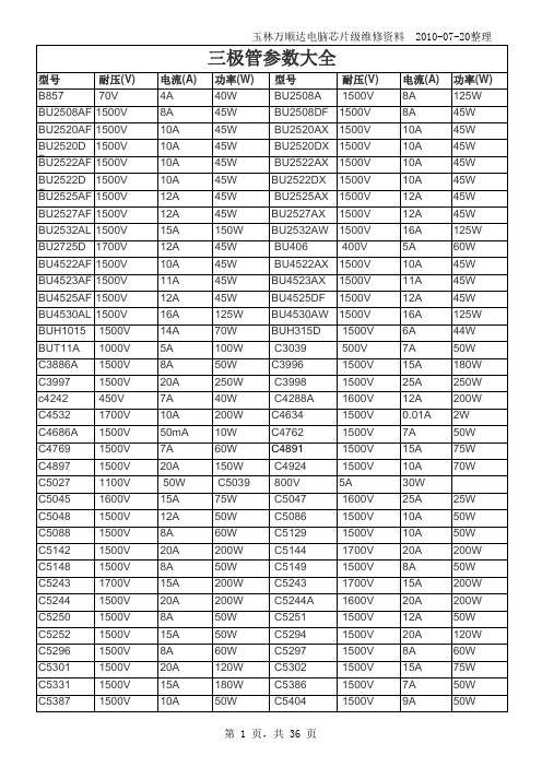
玉林万顺达电脑芯片级维修资料 2010-07-20整理玉林万顺达电脑芯片级维修资料 2010-07-20整理玉林万顺达电脑芯片级维修资料 2010-07-20整理玉林万顺达电脑芯片级维修资料 2010-07-20整理玉林万顺达电脑芯片级维修资料 2010-07-20整理玉林万顺达电脑芯片级维修资料 2010-07-20整理玉林万顺达电脑芯片级维修资料 2010-07-20整理玉林万顺达电脑芯片级维修资料 2010-07-20整理玉林万顺达电脑芯片级维修资料 2010-07-20整理玉林万顺达电脑芯片级维修资料 2010-07-20整理玉林万顺达电脑芯片级维修资料 2010-07-20整理玉林万顺达电脑芯片级维修资料 2010-07-20整理玉林万顺达电脑芯片级维修资料 2010-07-20整理玉林万顺达电脑芯片级维修资料 2010-07-20整理玉林万顺达电脑芯片级维修资料 2010-07-20整理玉林万顺达电脑芯片级维修资料 2010-07-20整理玉林万顺达电脑芯片级维修资料 2010-07-20整理玉林万顺达电脑芯片级维修资料 2010-07-20整理玉林万顺达电脑芯片级维修资料 2010-07-20整理玉林万顺达电脑芯片级维修资料 2010-07-20整理玉林万顺达电脑芯片级维修资料 2010-07-20整理玉林万顺达电脑芯片级维修资料 2010-07-20整理玉林万顺达电脑芯片级维修资料 2010-07-20整理玉林万顺达电脑芯片级维修资料 2010-07-20整理玉林万顺达电脑芯片级维修资料 2010-07-20整理玉林万顺达电脑芯片级维修资料 2010-07-20整理玉林万顺达电脑芯片级维修资料 2010-07-20整理玉林万顺达电脑芯片级维修资料 2010-07-20整理玉林万顺达电脑芯片级维修资料 2010-07-20整理玉林万顺达电脑芯片级维修资料 2010-07-20整理。

罗斯蒙特644温度变送器罗斯蒙特644温度变送器使用4 -20mA / HART 或基金会(FOUNDATION)现场息线协议可轻松进行通讯.符合MNAUR NE21标准,确保用于HART顶部接线盒安装产品的变送器性能可靠.与不匹配的装配件相比,变送器-传感器匹配特性将温度测量精度提高了75 % 。
一、产品特点.一体化LCD 显示器可便捷地显示主传感器输入信息和变送器诊断信息.安装准备解决方案提供了多种安装选项、变送器组态和传感器/热电偶1、针对控制应用领域的高精度和可靠性罗斯蒙特644 温度变送器是一种用于关键应用领域的理想产品(适用于多种过程环境)。
它为各种设备提供高精度测量,充分展示了Rosemount产品的可靠性。
罗斯蒙特644 可以与4-20mA /HART或全数字式基金会现场总线协议同时订购。
可对每个单元进行配置,以适应各类传感器的输入:热电阻、热电偶、毫伏表或欧姆表。
2、数字式现场设备提供动力采用HART或者现场总线通讯装置可确保高性能和先进诊断技术的良好发挥。
由此,这些变送器将信息传递给准备管理系统(AMS )。
性能。
此外,644 日AR 丁变送器还符合NAMUR NE 43 和NE 89 推荐标准。
3、可靠的变送器性能644HART变送器符合NAMUR NE21 推荐标准,它确保即使是在极为苛刻的电磁兼容性环境下也能保持一流的变送器。
此外,644HART变送器还符合NAMUR NE 43 和NE 89 推荐标准。
4、变送器与传感器匹配对于本质安全装置,只需一只安全栅就可为数台848 T型变将指定RTD 传感器的温度阻抗曲线图输入644 变送器后,变送器与传感器可获得完美的匹配。
这就避免了传感器的互换性错误,可将精度提高75 %。
5、安装灵活性DINA 型顶部接线盒安装变送器适用于各种远程变送器安装外壳,可以一体化或远程安装到一台传感器上。
紧凑导轨安装型极其适用于在密集型控制室内狭小空间中的DIN 导轨安装。

Electrical Specifications – Absolute RatingsStresses greater than those listed may cause permanent damage to the device. This is astress rating only, and functional operation of the device at these or any other condi-tions outside those indicated in the operational sections of this specification is not im-plied. Exposure to absolute maximum rating conditions for extended periods may affectreliability.Table 5: Absolute Maximum DC RatingsNotes: 1.V DD, V DDQ, and V DDL must be within 300mV of each other at all times; this is not re-quired when power is ramping down.2.V REFื 0.6 × V DDQ; however, V REF may be ุ V DDQ provided that V REFื 300mV.3.Voltage on any I/O may not exceed voltage on V DDQ.Temperature and Thermal ImpedanceIt is imperative that the DDR2 SDRAM device’s temperature specifications, shown inTable 6 (page 25), be maintained in order to ensure the junction temperature is in theproper operating range to meet data sheet specifications. An important step in main-taining the proper junction temperature is using the device’s thermal impedances cor-rectly. The thermal impedances are listed in Table 7 (page 27) for the applicable andavailable die revision and packages.Incorrectly using thermal impedances can produce significant errors. Read Microntechnical note TN-00-08, “Thermal Applications” (see /products/support/technical-notes), prior to using the thermal impedances listed in Table 7. Fordesigns that are expected to last several years and require the flexibility to use severalDRAM die shrinks, consider using final target theta values (rather than existing values)to account for increased thermal impedances from the die size reduction.The DDR2 SDRAM device’s safe junction temperature range can be maintained whenthe T C specification is not exceeded. In applications where the device’s ambient tem-perature is too high, use of forced air and/or heat sinks may be required in order to sat-isfy the case temperature specifications.Table 6: Temperature LimitsFigure 12: Example Temperature Test Point LocationLmm x Wmm FBGA质量等级领域:宇航级IC、特军级IC、超军级IC、普军级IC、禁运IC、工业级IC,军级二三极管,功率管等;应用领域:航空航天、船舶、汽车电子、军用计算机、铁路、医疗电子、通信网络、电力工业以及大型工业设备祝您:工作顺利,生活愉快!以深圳市美光存储技术有限公司提供的参数为例,以下为MT47H64M16NF-25E_M的详细参数,仅供参考Table 7: Thermal ImpedanceElectrical Specifications – I DD ParametersI DD Specifications and ConditionsTable 8: General I DD ParametersI DD7 ConditionsThe detailed timings are shown below for I DD7. Where general I DD parameters inTable 8 (page 28) conflict with pattern requirements of Table 9, then Table 9 require-ments take precedence.Table 9: I DD7 Timing Patterns (8-Bank Interleave READ Operation)Table 9: I DD7 Timing Patterns (8-Bank Interleave READ Operation) (Continued)Notes: 1. A = active; RA = read auto precharge; D = deselect.2.All banks are being interleaved at t RC (I DD) without violating t RRD (I DD) using a BL = 4.3.Control and address bus inputs are stable during deselects.。

Pin AssignmentPin#Front Side Pin#Back Side Pin#Front Side Pin#Back Side 1Vss 85Vss 43Vss 127Vss 2DQ086DQ3644OE2*128RFU 3DQ187DQ3745RAS2*129RAS3*4DQ288DQ3846CAS4*130CAS5*5DQ389DQ3947CAS6*131CAS7*6Vcc 90Vcc 48WE2*132PDE*7DQ491DQ4049Vcc 133Vcc 8DQ592DQ4150RFU 134RFU 9DQ693DQ4251RFU 135RFU 10DQ794DQ4352DQ18136DQ5411RFU 95RFU 53DQ19137DQ5512Vss 96Vss 54Vss 138Vss 13DQ997DQ4555DQ20139DQ5614DQ1098DQ4656DQ21140DQ5715DQ1199DQ4757DQ22141DQ5816DQ12100DQ4858DQ23142DQ5917DQ13101DQ4959Vcc 143Vcc 18Vcc 102Vcc 60DQ24144DQ6019DQ14103DQ5061RFU 145RFU 20DQ15104DQ5162RFU 146RFU 21DQ16105DQ5263RFU 147RFU 22RFU 106RFU 64RFU 148RFU 23Vss 107Vss 65DQ25149DQ6124RFU 108RFU 66RFU 150RFU 25RFU 109RFU 67DQ27151DQ6326Vcc 110Vcc 68Vss 152Vss 27WE0*111RFU 69DQ28153DQ6428CAS0*112CAS1*70DQ29154DQ6529CAS1*113CAS3*71DQ30155DQ6630RAS0*114RAS1*72DQ31156DQ6731OE0*115RFU 73Vcc 157Vcc 32Vss 116Vss 74DQ32158DQ6833A0117A175DQ33159DQ6934A2118A376DQ34160DQ7035A4119A577RFU 161RFU 36A6120A778Vss 162Vss 37A8121A979PD1163PD238A10122A1180PD3164PD439A12123RFU 81PD5165PD640Vcc 124Vcc 82PD7166PD841RFU 125RFU 83ID0167ID142RFU126BO84Vcc168Vcc* Active LowExtended Data Out (EDO) DRAM DIMM6416AsEDM4G18TK 168 Pin 16Mx64 EDO DIMM Buffered, 4k Refresh, 3.3V Features• JEDEC-Standard 168-pin Dual Inline MemoryModule (DIMM)• Buffered• Supports Extended Data-out (EDO) access cycles • Based on 8Mx8 DRAM • Power Supply: 3.3V ± 0.3V • 64ms, 4096-cycle refresh• Supports RAS-Only-Refresh (ROR), CAS-before-RAS (CBR) refresh and Hidden refresh cycles • Serial Presence Detect (SPD)• LVTTL Compatible Inputs and Outputs • Two External Banks • Gold PCB connectorGeneral DescriptionThe 6416AsEDM4G18TK is a 16Mx64 bit, 18chip, 3.3V, 168 Pin DIMM module consisting of (16)8Mx8 (TSOP) DRAMs and (2) Buffers. The module is buffered and supports Extended Data Out (EDO) page mode access.Valid Part NumbersPart Number Access Time Supply Voltage 6416A5EDM4G18TK 50ns 3.3V 6416A6EDM4G18TK60ns3.3VBlock DiagramA1 - ANA1 - AN: DRAMs U1 - U18VCCVSS U1 - U18U1 - U18PRESENCE DETECT RESISTORS: R1-R5B0U1, U7 - U10, U15 - U18A0U1, U3 - U6, U11 - U14Presence Detect MatrixDIMM TypePD1PD2PD3PD4PD5PD6PD7PD8ID0ID16416A5EDM4G018TK Vss NC NC NC NC Vss Vss NC Vss Vss 6416A6EDM4G018TKVssNCNCNCNCNCNCNCVssVssPin DescriptionsPin NameFunctionRAS#Row Address Strobe RAS# is used to strobe the row address.CAS#Column Address Strobe CAS# is used to strobe the column address.WE#Write Enable WE# is used to control read/write cycles.OE#Output Enable OE# is the input/output control for the DQ lines.A#, B0Address Lines Address lines are multiplexed to specify the row and column address.DQ0-DQ71Data Lines Data input/output lines.Vdd Power Supply Power Supply 3.3V ±0.3V VssGroundGroundPD#, ID#Presence Detect Lines Presence detect lines used to indicate module type.PDE Presence Detect Enable Enables buffers on PD lines.NCNo ConnectionLine is not connected in DIMM.Absolute Maximum RatingsParameter Symbol Value UnitsVoltage on any pin relative to Vss V in-0.5 to 4.6VShort circuit output current I out50mAPower dissipation Pt18WOperating temperature T opr0 to +70°CStorage temperature T st-55 to +125°CNOTE: Permanent damage may occur if absolute maximum ratings are exceeded.Device should be operated within recommended operating conditions only.DC Characteristics (T A = 0 to 70C, Vcc = 3.3V ± 0.3V)Parameter Symbol Min Typ Max Units Note Supply voltage Vss000VSupply voltage Vcc 3.0 3.3 3.6V16 Input high voltage Vih 2.0-Vcc+0.3V16 Input low voltage Vil-0.3-0.3V16 Output high voltage Voh 2.4--VOutput low voltage Vol--0.8VDC Current Consumption (T A = 0 to 70C, Vcc = 3.3V ± 0.3V)Parameter Symbol Test Condition-50-60Unit Note Standby Current (TTL)I CC1(RAS# = CAS# = V IH)3232mA17 Standby Current (CMOS)I CC2All inputs = Vcc - 0.2V1616mA17 Operating Current Random Read/Write I CC3RAS#, CAS#, address cycling. t RC = t RC[MIN]13601120mA17, 18 Operating Current Fast Page Mode I CC4RAS# = V IL, CAS#, Address cycling. t PC = t PC[MIN]N/A N/A mA17, 18 Operating Current EDO Page Mode I CC5RAS# = V IL, CAS#, Address cycling. t PC = t PC[MIN]976784mA17, 18 Refresh Current: RAS#-Only I CC6RAS# cycling, CAS#=V IH; t RC = t RC[MIN]12641072mA17 Refresh Current: CAS# before RAS#I CC7RAS#, CAS#, address cycling t RC = t RC[MIN]13601120mA17Capacitance (T A = 0 to 70C, Vcc = 3.3V ± 0.3V, Vss = 0V)Parameter Symbol Typ Max Units NoteInput capacitance (Address)C I1-5pFInput capacitance (WE#, OE#)C I2-7pFInput/Output capacitance (Data)C I/O-14pFInput capacitance (CAS#)C I3-7pFInput capacitance (RAS#)C14-28pFAC Characteristics (T A = 0 to 70C, Vcc = 3.3V ± 0.3V, Vss = 0V)Units Note Parameter Symbol-50-60Min Max Min MaxAccess time from column address t AA2530ns3, 5, 14 Column address setup to CAS# precharge t ACH1215nsColumn address hold time (from RAS#)t AR4050nsColumn address setup time t ASC00nsRow address setup time t ASR00nsAccess time from CAS#t CAC1517ns3, 4, 14 Column address hold time t CAH810nsCAS# pulse width t CAS810 0001010 000nsCAS# to output in Low-Z t CLZ33nsData output hold after CAS# LOW t COH33nsCAS# precharge time t CP810nsAccess time from CAS# precharge t CPA2835nsCAS# to RAS# precharge time t CRP55nsCAS# hold time t CSH4050nsWRITE command to CAS# lead time t CWL810nsData-in hold time t DH810ns11 Data-in setup time t DS00ns11 Output buffer turn-off delay t OFF012015nsEDO Page-mode read or write cycle time t PC2025nsAccess time from RAS#t RAC5060ns2, 3 RAS# to column address delay time t RAD15251530ns9 Row-address hold time t RAH1010nsRAS# pulse width t RAS, t RASP5010 0006010 000nsRandom read/write cycle time t RC84104nsRAS# to CAS# delay time t RCD20352043ns8 Read command hold time t RCH00nsRead command setup time t RCS00nsRefresh Period (4.096 cycles)t REF6464ms15 RAS# precharge time t RP3040nsRAS# to CAS# precharge time t RPC55nsREAD command hold time t RRH00nsRAS# hold time t RSH1317nsWRITE command to RAS# lead time t RWL1315nsTransition Time tτ250250ns7AC Characteristics (T A = 0 to 70C, Vcc = 3.3V ± 0.3V, Vss = 0V)Units Note Parameter Symbol-50-60Min Max Min MaxWRITE command hold time t WCH810nsWRITE command hold time (RAS# referenced)t WCR3845nsWE# command setup time t WCS00ns10 Output disable delay from WE#t WHZ012015nsWrite command pulse width t WP55nsNotes1.AC measurements assume t T = 5ns2.Assumes that t RCD≤ t RCD (max.) and t RAD≥ t RAD (max.). If t RCD or t RAD is greater that the maximum recommended value shown in this table, t RACexceeds the value shown.3.Measured with a load circuit equivilaent to 1 TTL load and 100pF.4.Assumes that t RCD≥ t RCD (max.), t RAD≤ t RAD (max.).5.Assumes that t RCD≤ t RCD (max.), t RAD≥ t RAD (max.).6.t OFF (max.) defines the time at which the output achieves the open circuit condition and is not referenced to output voltage levels.7.Vih (min.) and Vil (max.) are reference levels for measuring timing of input signals. Also, transition times are measured between Vih and Vil.8.Operation with the t RCD (max.) limit insures that t RAC (max.) can be met, t RCD (max.) is specified as a reference point only, if t RCD is greater that thespecified t RCD (max.) limit, then the access time is controlled exclusively by t CAC.9.Operation with the t RAD (max.) limit insures that t RAC (max.) can be met, t RAD (max.) is specified as a reference point only, if t RAD is greater that thespecified t RAD (max.) limit, then access time is controlled exclusively by t AA.10.Early write cycle only (t WCS≥ t WCS (min.))11.These parameters are referenced to CAS* leading edge in an early write cycle.12.An initial pause of 100us is required after power up followed by a minimum of eight initialization cycles (any combination of cycles containing RAS*clock such as RAS* only refresh)13.t RASC defines RAS* pulse width in fast page mode cycles.14.Access time is determined by the longer of t AA or t CAC or t ACP15.t REF defined is 4,096 refresh cycle.16.All voltages referenced to Vss17.Typical maximum current consumption levels18.Column address changed once per cycletRPt RASt RC t CRPt RCDt CASt RSHt CSH t RRHt ASRt RAHt RADt ACHt CAH t ASCt ARt RCSt RCHt CLZt CAC t RAC t AA t OFFADDRWEDQ CASRASROWCOLUMNROWVALID DATAOPENOPENREAD CYCLEDON'T CAREUNDEFINEDt RPt RASt RC t CRPt RCDt CASt RSH t CSHt ASRt RAHt RADt ACHt CAH t ASC t AR t WPt WCH t WCR t RWLADDRDQ CASROWCOLUMNROWVALID DATAEARLY WRITE CYCLEDON'T CARE UNDEFINEDt WCSt CWL t DHt DStRPtRASPtCRPtRCDtCSHtCAStCPtCAStPCtCPtCAStRSHtCPtASRtRAHtRADtARtASCtCAHtASCtCAHtASCtCAHtRCStRCHtOFFtCLZtCACtCPAtAAtCOHtCACtCPAtAAtCLZtCACtRACtAAADDRWEDQDON'T CAREUNDEFINED ROW ROWCOLUMNCOLUMN COLUMNVALIDDATAVALIDDATAVALIDDATAEDO-PAGE-MODE READ CYCLEtACHtCAHtCAHtRRH OPENOPENtRPtRASPtCRPtRCDtCSHtCAStCPtCAStPCtCPtCAStRSHtCPtASRtRAHtRADtARtASCtCAHtASCtCAHtASCtCAHtDHtDStCOHtCACtCACtRACADDRWEDQCASRASDON'T CAREUNDEFINED ROW ROWCOLUMN (B)COLUMN (A)COLUMN (N)VALID Dout VALID Dout VALID DinEDO-PAGE-MODE READ-EARLY-WRITE CYCLEtACHtRCHtAAtPCtWCStWCHtRCStWHZtCPAtAAOPENtRPtRASPtCRPtRCDtCSHtCAStCPtCAStPCtCPtCAStRSHtCPtASRtRAHtRADtARtASCtCAHtASCtCAHtASCtCAHtWPtWPtWPtDHtDStDHtDStCACtWCRADDRWEDQCASRASDON'T CAREUNDEFINED ROW ROWCOLUMNCOLUMN COLUMNVALID DATA VALID DATA VALID DATAFAST/EDO-PAGE-MODE EARLY-WRITE CYCLEtACHtACHtACHtWCHtCWLtWCStWCHtCWLtWCStWCHtCWLtWCStDStRWLtCRPtRCDtCSHtCAStCPtASRtRAHtRADtASCtCAHtARtASCROW COLUMN COLUMNtRCStRCHtWPZtRCSOPENtCLZtCACtRACtAAtWHZOPENtCLZDON'T CAREUNDEFINEDVALID DATAEDO READ CYCLE( with /WE-controlled disable )ADDRWEDQCASRASt RPt RASt RCtCRPt RPCt ASRt RAHROWROWOPEN/RAS-ONLY REFRESH CYCLEDON'T CARE UNDEFINEDADDRQ RASWECASL / CASHt RPt RASt CPt CHROPENDON'T CARE UNDEFINEDt RPt RASt RPC t CSRt RPCt CSRt CHRt WRP t WRHt WRP t WRHWEDQCASRASCBR REFRESH CYCLE( Addresses = DON'T CARE )16M x 64 Bit 3.3V16Mx64 BUFERED 3.3V EDO DIMM DS531-0 12-17-96PNY Technologies Reserves the right to change products or specifications without notice©1998 PNY Technologies, Inc. 11元器件交易网。

DOUBLE DATA RATE (DDR) SDRAM MT46V128M4 –32 Meg x4x 4 banks MT46V64M8 –16 Meg x8x4 banks MT46V32M16 –8 Meg x16 x4 banks For the latest data sheet revisions, please refer to the Micron Web site: /datasheets/ddrsdramds.htmlFEATURES•V DD = +2.5V ±0.2V, V DD Q = +2.5V ±0.2V•Bidirectional data strobe (DQS) transmitted/received with data, i.e., source-synchronous datacapture (x16 has two – one per byte)•Internal, pipelined double-data-rate (DDR)architecture; two data accesses per clock cycle•Differential clock inputs (CK and CK#)•Commands entered on each positive CK edge•DQS edge-aligned with data for READs; center-aligned with data for WRITEs•DLL to align DQ and DQS transitions with CK•Four internal banks for concurrent operation•Data mask (DM) for masking write data (x16 hastwo – one per byte)•Programmable burst lengths: 2, 4, or 8•Auto precharge option•Auto Refresh and Self Refresh Modes•Longer lead TSOP for improved reliability (OCPL)• 2.5V I/O (SSTL_2 compatible)OPTIONS MARKING•Configuration128 Meg x 4(32 Meg x4 x 4 banks)128M464 Meg x 8(16 Meg x8 x 4 banks)64M832 Meg x 16(8 Meg x16 x 4 banks)32M16•x16 IOL / IOH DriveFull Drive Only D1Reduced Drive Only D2Programmable full or reduced drive D3•Plastic Package – OCPL66-pin TSOP (standard 22.3mm length)TG66-pin TSOP (extended 27mm length)TH(400 mil width, 0.65mm pin pitch)•Timing – Cycle Time7.5ns @ CL = 2 (DDR266A+)1-77.5ns @ CL =2.5 (DDR266B)2-7510ns @ CL =2 (DDR200)3-8•Self RefreshStandard noneLow Power LNOTE: 1.Supports PC2100 modules with 2-2-2 timing2.Supports PC2100 modules with 2.5-3-3 timing3.Supports PC1600 modules with 2-2-2 timing*Minimum clock rate @ CL = 2 (-7, -8) and CL = 2.5 (-75)**CL = CAS (Read) Latency512Mb: x4, x8, x16 DDR SDRAM Micron Technology, Inc., reserves the right to change products or specifications without notice.GENERAL DESCRIPTIONThe 512Mb DDR SDRAM is a high-speed CMOS, dynamic random-access memory containing 536,870,912 bits. It is internally configured as a quad-bank DRAM.The 512Mb DDR SDRAM uses a double data rate architecture to achieve high-speed operation. The double data rate architecture is essentially a 2n-prefetch architecture with an interface designed to transfer two data words per clock cycle at the I/O pins. A single read or write access for the 512Mb DDR SDRAM effectively consists of a single 2n-bit wide, one-clock-cycle data transfer at the internal DRAM core and two corre-sponding n-bit wide, one-half-clock-cycle data trans-fers at the I/O pins.A bidirectional data strobe (DQS) is transmitted externally, along with data, for use in data capture at the receiver. DQS is a strobe transmitted by the DDR SDRAM during READs and by the memory controller during WRITE s. DQS is edge-aligned with data for READs and center-aligned with data for WRITEs. The x16 offering has two data strobes, one for the lower byte and one for the upper byte.The 512Mb DDR SDRAM operates from a differen-tial clock (CK and CK#); the crossing of CK going HIGH and CK# going LOW will be referred to as the positive edge of CK. Commands (address and control signals) are registered at every positive edge of CK. Input data is registered on both edges of DQS, and output data is referenced to both edges of DQS, as well as to both edges of CK.Read and write accesses to the DDR SDRAM are burst oriented; accesses start at a selected location and continue for a programmed number of locations in a programmed sequence. Accesses begin with the regis-tration of an ACTIVE command, which is then fol-lowed by a RE AD or WRITE command. The address bits registered coincident with the ACTIVE command are used to select the bank and row to be accessed. The address bits registered coincident with the RE AD or WRITE command are used to select the bank and the starting column location for the burst access.The DDR SDRAM provides for programmable READ or WRITE burst lengths of 2, 4, or 8 locations. An auto precharge function may be enabled to provide a self-timed row precharge that is initiated at the end of the burst access.As with standard SDR SDRAMs, the pipelined, multibank architecture of DDR SDRAMs allows for concurrent operation, thereby providing high effective bandwidth by hiding row precharge and activation time.An auto refresh mode is provided, along with a power-saving power-down mode. All inputs are com-patible with the JE DE C Standard for SSTL_2. All full drive strength outputs are SSTL_2, Class II compatible. NOTE: 1.The functionality and the timing specificationsdiscussed in this data sheet are for the DLL-enabledmode of operation.2.Throughout the data sheet, the various figures andtext refer to DQs as “DQ.” The DQ term is to beinterpreted as any and all DQ collectively, unlessspecifically stated otherwise. Additionally, the x16is divided in to two bytes—the lower byte and upperbyte. For the lower byte (DQ0 through DQ7) DMrefers to LDM and DQS refers to LDQS; and for theupper byte (DQ8 through DQ15) DM refers to UDMand DQS refers to UDQS.(Note: xx= 7, 75, or 8)256Mb DDR SDRAM PART NUMBERSTABLE OF CONTENTSFunctional Block Diagram – 128 Meg x 4 (4)Functional Block Diagram – 64 Meg x 8 (5)Functional Block Diagram – 32 Meg x 16 (6)Pin Descriptions (7)Functional Description (9)Initialization (9)Register Definition (9)Mode Register (9)Burst Length (9)Burst Type (10)Read Latency (11)Operating Mode (11)Extended Mode Register (12)DLL E nable/Disable (12)Commands (13)Truth Table 1 (Commands) (13)Truth Table 1A (DM Operation) (13)Deselect (14)No Operation (NOP) (14)Load Mode Register (14)Active (14)Read (14)Write (14)Precharge (14)Auto Precharge (14)Burst Terminate (14)Auto Refresh (15)Self Refresh (15)Operation (16)Bank/Row Activation (16)Reads (17)Read Burst (18)Consecutive Read Bursts (19)Nonconsecutive Read Bursts (20)Random Read Accesses (21)Terminating a Read Burst (23)Read to Write (24)Read to Precharge (25)Writes (26)Write Burst (27)Consecutive Write to Write (28)Nonconsecutive Write to Write (29)Random Writes (30)Write to Read – Uninterrupting (31)Write to Read – Interrupting (32)Write to Read – Odd, Interrupting (33)Write to Precharge – Uninterrupting (34)Write to Precharge – Interrupting (35)Write to Precharge – Odd, Interrupting (36)Precharge (37)Power-Down (37)Truth Table 2 (CKE) (38)Truth Table 3 (Current State, Same Bank) (39)Truth Table 4 (Current State, Different Bank) (41)Operating ConditionsAbsolute Maximum Ratings (43)DC Electrical and Operating Conditions (43)AC Input Operating Conditions (43)Capacitance – x4, x8 (44)I DD Specifications and Conditions – x4, x8 (45)Capacitance – x16 (46)I DD Specifications and Conditions – x16 (47)AC Electrical Characteristics (Timing Table) (48)Slew Rate Derating Table (49)Data Valid Window Derating (51)Voltage and Timing WaveformsNominal Output Drive Curves (54)Reduced Output Drive Curves (x16 only) (55)Output Timing – t DQSQ and t QH - x4, x8 (56)Output Timing – t DQSQ and t QH - x16 (57)Output Timing – t AC and t DQSCK (58)Input Timing (58)Input Voltage (59)Initialize and Load Mode Registers (60)Power-Down Mode (61)Auto Refresh Mode (62)Self Refresh Mode (63)ReadsBank Read - Without Auto Precharge (64)Bank Read - With Auto Precharge (65)WritesBank Write – Without Auto Precharge (66)Bank Write – With Auto Precharge (67)Write – DM Operation (68)66-pin TSOP (TH) dimensions (69)66-pin TSOP (TG) dimensions (70)FUNCTIONAL BLOCK DIAGRAM128 Meg x 4A0-A12,BA0, BA1FUNCTIONAL BLOCK DIAGRAM64 Meg x 8A0-A12,BA0, BA1FUNCTIONAL BLOCK DIAGRAM32 Meg x 16A0-A12,BA0, BA1PIN DESCRIPTIONS(continued on next page)PIN DESCRIPTIONS (continued)RESERVED NC PINS1NOTE: 1. NC pins not listed may also be reserved for other uses now or in the future. This table simply defines specific NC pins deemed to be of importance.FUNCTIONAL DESCRIPTIONThe 512Mb DDR SDRAM is a high-speed CMOS, dynamic random-access memory containing 536,870,912 bits. The 512Mb DDR SDRAM is internally configured as a quad-bank DRAM.The 512Mb DDR SDRAM uses a double data rate architecture to achieve high-speed operation. The double data rate architecture is essentially a 2n-prefetch architecture, with an interface designed to transfer two data words per clock cycle at the I/O pins. A single read or write access for the 512Mb DDR SDRAM consists of a single 2n-bit wide, one-clock-cycle data transfer at the internal DRAM core and two corresponding n-bit wide, one-half-clock-cycle data transfers at the I/O pins.Read and write accesses to the DDR SDRAM are burst oriented; accesses start at a selected location and continue for a programmed number of locations in a programmed sequence. Accesses begin with the regis-tration of an ACTIVE command, which is then fol-lowed by a RE AD or WRITE command. The address bits registered coincident with the ACTIVE command are used to select the bank and row to be accessed (BA0, BA1 select the bank; A0-A12 select the row). The ad-dress bits registered coincident with the RE AD or WRITE command are used to select the starting column loca-tion for the burst access.Prior to normal operation, the DDR SDRAM must be initialized. The following sections provide detailed information covering device initialization, register defi-nition, command descriptions and device operation. InitializationDDR SDRAMs must be powered up and initialized in a predefined manner. Operational procedures other than those specified may result in undefined opera-tion. Power must first be applied to V DD and V DD Q simultaneously, and then to V REF (and to the system V TT). V TT must be applied after V DD Q to avoid device latch-up, which may cause permanent damage to the device. V REF can be applied any time after V DD Q but is expected to be nominally coincident with V TT. Except for CKE, inputs are not recognized as valid until after V REF is applied. CKE is an SSTL_2 input but will detect an LVCMOS LOW level after V DD is applied. Maintain-ing an LVCMOS LOW level on CKE during power-up is required to ensure that the DQ and DQS outputs will be in the High-Z state, where they will remain until driven in normal operation (by a read access). After all power supply and reference voltages are stable, and the clock is stable, the DDR SDRAM requires a 200µs delay prior to applying an executable command.Once the 200µs delay has been satisfied, a DE SE-LECT or NOP command should be applied, and CKE should be brought HIGH. Following the NOP com-mand, a PRE CHARGE ALL command should be ap-plied. Next a LOAD MODE RE GISTE R command should be issued for the extended mode register (BA1 LOW and BA0 HIGH) to enable the DLL, followed by another LOAD MODE RE GISTE R command to the mode register (BA0/BA1 both LOW) to reset the DLL and to program the operating parameters. Two-hun-dred clock cycles are required between the DLL reset and any RE AD command. A PRE CHARGE ALL com-mand should then be applied, placing the device in the all banks idle state.Once in the idle state, two AUTO REFRESH cycles must be performed (t RFC must be satisfied.) Addition-ally, a LOAD MODE RE GISTE R command for the mode register with the reset DLL bit deactivated (i.e., to program operating parameters without resetting the DLL) is required. Following these requirements, the DDR SDRAM is ready for normal operation. Register DefinitionMODE REGISTERThe mode register is used to define the specific mode of operation of the DDR SDRAM. This definition includes the selection of a burst length, a burst type, a CAS latency and an operating mode, as shown in Figure 1. The mode register is programmed via the MODE RE GISTE R SE T command (with BA0 = 0 and BA1 = 0) and will retain the stored information until it is programmed again or the device loses power (except for bit A8, which is self-clearing).Reprogramming the mode register will not alter the contents of the memory, provided it is performed correctly. The mode register must be loaded (reloaded) when all banks are idle and no bursts are in progress, and the controller must wait the specified time before initiating the subsequent operation. Violating either of these requirements will result in unspecified operation.Mode register bits A0-A2 specify the burst length, A3 specifies the type of burst (sequential or interleaved), A4-A6 specify the CAS latency, and A7-A12 specify the operating mode.Burst LengthRead and write accesses to the DDR SDRAM are burst oriented, with the burst length being program-mable, as shown in Figure 1. The burst length deter-mines the maximum number of column locations that can be accessed for a given READ or WRITE command. Burst lengths of 2, 4, or 8 locations are available for both the sequential and the interleaved burst types.Figure 1Mode Register DefinitionReserved states should not be used, as unknown operation or incompatibility with future versions may result.When a RE AD or WRITE command is issued, a block of columns equal to the burst length is effectively selected. All accesses for that burst take place within this block, meaning that the burst will wrap within the block if a boundary is reached. The block is uniquely selected by A1-A i when the burst length is set to two, by A2-A i when the burst length is set to four and by A3-A i when the burst length is set to eight (where A i is the most significant column address bit for a given con-figuration). The remaining (least significant) addressTable 1Burst DefinitionNOTE: 1.For a burst length of two, A1-A i select the two-data-element block; A0 selects the first access within the block.2.For a burst length of four, A2-A i select the four-data-element block; A0-A1 select the first access within the block.3.For a burst length of eight, A3-A i select the eight-data-element block; A0-A2 select the first access within the block.4.Whenever a boundary of the block is reached within a given sequence above, the following access wraps within the block.bit(s) is (are) used to select the starting location within the block. The programmed burst length applies to both READ and WRITE bursts.Burst TypeAccesses within a given burst may be programmed to be either sequential or interleaved; this is referred to as the burst type and is selected via bit M3.The ordering of accesses within a burst is deter-mined by the burst length, the burst type and the starting column address, as shown in Table 1.A9A7A6A5A4A3A8A2A1A0Address BusA10A12A11BA1BA0Table 2CAS Latency (CL)Read LatencyThe RE AD latency is the delay, in clock cycles,between the registration of a READ command and the availability of the first bit of output data. The latency can be set to 2, or 2.5 clocks, as shown in Figure 2.If a READ command is registered at clock edge n ,and the latency is m clocks, the data will be available nominally coincident with clock edge n + m . Table 2indicates the operating frequencies at which each CAS latency setting can be used.Reserved states should not be used as unknown operation or incompatibility with future versions may result.Figure 2CAS LatencyRE GISTE R SE T command with bits A7-A12R command is issued to reset the DLL, itFigure 3Extended Mode Register DefinitionEXTENDED MODE REGISTERThe extended mode register controls functions be-yond those controlled by the mode register; these additional functions are DLL enable/disable and output drive strength. These functions are controlled via the bits shown in Figure 3. The extended mode register is programmed via the LOAD MODE RE GIS-TER command to the mode register (with BA0 = 1 and BA1 = 0) and will retain the stored information until it is programmed again or the device loses power. The enabling of the DLL should always be followed by a LOAD MODE REGISTER command to the mode regis-ter (BA0/BA1 both LOW) to reset the DLL.The extended mode register must be loaded when all banks are idle and no bursts are in progress, and the controller must wait the specified time before initiating any subsequent operation. Violating either of these requirements could result in unspecified operation.Output Drive StrengthThe normal drive strength for all outputs are speci-fied to be SSTL2, Class II. The x16 supports an option for reduced drive. This option is intended for the support of the lighter load and/or point-to-point environments. The selection of the reduced drive strength will alter the DQs and DQSs from SSTL2, Class II drive strength to a reduced drive strength, which is approximately 54% of the SSTL2, Class II drive strength.Micron will support these x16 options: 1) Full drive strength only (not programmable), 2) Reduced drive strength only (not programable), and 3) Program-mable full or reduced drive strength.DLL Enable/DisableThe DLL must be enabled for normal operation.DLL enable is required during power-up initialization and upon returning to normal operation after having disabled the DLL for the purpose of debug or evalua-tion. (When the device exits self refresh mode, the DLL is enabled automatically.) Any time the DLL is enabled,200 clock cycles must occur before a READ command can be issued.A9A7A6A5A4A3A8A2A1A0Address BusA10A11A12BA0BA1NOTE: 1. E14 and E13 (BA0 and BA1) must be “1, 0” to select theExtended Mode Register (vs. the base Mode Register). 2. The reduced drive strength option is not supported onthe x4 and x8 versions: and is only available on the D3 versionof the x16 device.3. The QFC# option is not supported.appear following the Operation section; these tables provide current state/next state information.COMMANDSTruth Table 1 provides a quick reference of avail-able commands. This is followed by a verbal descrip-tion of each command. Two additional Truth TablesNOTE: 1.CKE is HIGH for all commands shown except SELF REFRESH.2.BA0-BA1 select either the mode register or the extended mode register (BA0 = 0, BA1 = 0 select the mode register;BA0 = 1, BA1 = 0 select extended mode register; other combinations of BA0-BA1 are reserved). A0-A12 provide the op-code to be written to the selected mode register.3.BA0-BA1 provide bank address and A0-A12 provide row address.4.BA0-BA1 provide bank address; A0-A i provide column address (where i = 9 for x16, 9,11 for x8, and 9, 11, 12 for x4);A10 HIGH enables the auto precharge feature (nonpersistent), and A10 LOW disables the auto precharge feature.5.A10 LOW: BA0-BA1 determine which bank is precharged.A10 HIGH: all banks are precharged and BA0-BA1 are “Don ’t Care.”6.This command is AUTO REFRESH if CKE is HIGH, SELF REFRESH if CKE is LOW.7.Internal refresh counter controls row addressing; all inputs and I/Os are “Don ’t Care ” except for CKE.8.Applies only to read bursts with auto precharge disabled; this command is undefined (and should not be used) for READ bursts with auto precharge enabled and for WRITE bursts.9.DESELECT and NOP are functionally interchangeable.ed to mask write data; provided coincident with the corresponding data.TRUTH TABLE 1 – COMMANDS(Note: 1)TRUTH TABLE 1A – DM OPERATION(Note: 10)DESELECTThe DESELECT function (CS# HIGH) prevents new commands from being executed by the DDR SDRAM. The DDR SDRAM is effectively deselected. Operations already in progress are not affected.NO OPERATION (NOP)The NO OPE RATION (NOP) command is used to instruct the selected DDR SDRAM to perform a NOP (CS# LOW). This prevents unwanted commands from being registered during idle or wait states. Operations already in progress are not affected.LOAD MODE REGISTERThe mode registers are loaded via inputs A0–A12. See mode register descriptions in the Register Defini-tion section. The LOAD MODE REGISTER command can only be issued when all banks are idle, and a subsequent executable command cannot be issued until t MRD is met.ACTIVEThe ACTIVE command is used to open (or activate) a row in a particular bank for a subsequent access. The value on the BA0, BA1 inputs selects the bank, and the address provided on inputs A0–A12 selects the row. This row remains active (or open) for accesses until a PRE CHARGE command is issued to that bank.A PRECHARGE command must be issued before open-ing a different row in the same bank.READThe READ command is used to initiate a burst read access to an active row. The value on the BA0, BA1 inputs selects the bank, and the address provided on inputs A0–A i (where i = 9 for x16; 9, 11 for x8; or 9, 11, and 12 for x4) selects the starting column location. The value on input A10 determines whether or not auto precharge is used. If auto precharge is selected, the row being accessed will be precharged at the end of the READ burst; if auto precharge is not selected, the row will remain open for subsequent accesses.WRITEThe WRITE command is used to initiate a burst write access to an active row. The value on the BA0, BA1 inputs selects the bank, and the address provided on inputs A0–A i (where i = 9 for x16; 9 and 11 for x8; or 9, 11, and 12 for x4) selects the starting column location. The value on input A10 determines whether or not auto precharge is used. If auto precharge is selected, the row being accessed will be precharged at the end of the WRITE burst; if auto precharge is not selected, the row will remain open for subsequent accesses. Input data appearing on the DQs is written to the memory array subject to the DM input logic level appearing coincident with the data. If a given DM signal is registered LOW, the corresponding data will be written to memory; if the DM signal is registered HIGH, the corresponding data inputs will be ignored, and a WRITE will not be executed to that byte/column location.PRECHARGEThe PRECHARGE command is used to deactivate the open row in a particular bank or the open row in all banks. The bank(s) will be available for a subsequent row access a specified time (t RP) after the PRECHARGE com-mand is issued. Input A10 determines whether one or all banks are to be precharged, and in the case where only one bank is to be precharged, inputs BA0, BA1 select the bank. Otherwise BA0, BA1 are treated as “Don’t Care.”Once a bank has been precharged, it is in the idle state and must be activated prior to any RE AD or WRITE commands being issued to that bank. A PRECHARGE command will be treated as a NOP if there is no open row in that bank (idle state), or if the previously open row is already in the process of precharging.AUTO PRECHARGEAuto precharge is a feature which performs the same individual-bank precharge function described above, but without requiring an explicit command. This is accomplished by using A10 to enable auto precharge in conjunction with a specific RE AD or WRITE command. A precharge of the bank/row that is addressed with the READ or WRITE command is auto-matically performed upon completion of the READ or WRITE burst. Auto precharge is nonpersistent in that it is either enabled or disabled for each individual READ or WRITE command.Auto precharge ensures that the precharge is initi-ated at the earliest valid stage within a burst. This “earliest valid stage” is determined as if an explicit PRECHARGE command was issued at the earliest pos-sible time, without violating t RAS (MIN), as described for each burst type in the Operation section of this data sheet. The user must not issue another command to the same bank until the precharge time (t RP) is completed. BURST TERMINATEThe BURST TERMINATE command is used to trun-cate READ bursts (with auto precharge disabled). The most recently registered READ command prior to the BURST TE RMINATE command will be truncated, as shown in the Operation section of this data sheet. The open page which the READ burst was terminated from remains open.AUTO REFRESHAUTO RE FRE SH is used during normal operation of the DDR SDRAM and is analogous to CAS#-BE-FORE-RAS# (CBR) RE FRE SH in FPM/E DO DRAMs. This command is nonpersistent, so it must be issued each time a refresh is required.The addressing is generated by the internal refresh controller. This makes the address bits a “Don’t Care”during an AUTO RE FRE SH command. The 512Mb DDR SDRAM requires AUTO RE FRE SH cycles at an average interval of 7.8125µs (maximum).To allow for improved efficiency in scheduling and switching between tasks, some flexibility in the abso-lute refresh interval is provided. A maximum of eight AUTO REFRESH command can be posted to any given DDR SDRAM, meaning that the maximum absolute interval between any AUTO REFRESH command and the next AUTO RE FRE SH command is 9 × 7.8125µs (70.3µs). This maximum absolute interval is to allow future support for DLL updates internal to the DDR SDRAM to be restricted to AUTO RE FRE SH cycles, without allowing excessive drift in t AC between up-dates.Although not a JEDEC requirement, to provide for future functionality features, CKE must be active (High)during the AUTO RE FRE SH period. The AUTO RE-FRESH period begins when the AUTO REFRESH com-mand is registered and ends t RFC latter.SELF REFRESHThe SELF REFRESH command can be used to retain data in the DDR SDRAM, even if the rest of the system is powered down. When in the self refresh mode, the DDR SDRAM retains data without external clocking. The SELF REFRESH command is initiated like an AUTO RE FRE SH command except CKE is disabled (LOW). The DLL is automatically disabled upon entering SELF RE FRE SH and is automatically enabled upon exiting SELF REFRESH (200 clock cycles must then occur before a READ command can be issued). Input signals except CKE are “Don’t Care” during SELF REFRESH.The procedure for exiting self refresh requires a sequence of commands. First, CK must be stable prior to CKE going back HIGH. Once CKE is HIGH, the DDR SDRAM must have NOP commands issued for t XSNR because time is required for the completion of any internal refresh in progress. A simple algorithm for meeting both refresh and DLL requirements is to apply NOPs for 200 clock cycles before applying any other command.OperationsBANK/ROW ACTIVATIONBefore any RE AD or WRITE commands can be issued to a bank within the DDR SDRAM, a row in that bank must be “opened.” This is accomplished via the ACTIVE command, which selects both the bank and the row to be activated, as shown in Figure 4.After a row is opened with an ACTIVE command,a RE AD or WRITE command may be issued to that row, subject to the t RCD specification. t RCD (MIN)should be divided by the clock period and rounded up to the next whole number to determine the earliest clock edge after the ACTIVE command on which a RE AD or WRITE command can be entered. For ex-ample, a t RCD specification of 20ns with a 133 MHz clock (7.5ns period) results in 2.7 clocks rounded to 3.This is reflected in Figure 5, which covers any case where 2 < t RCD (MIN)/t CK ≤ 3. (Figure 5 also shows the same case for t RCD; the same procedure is used to convert other specification limits from time units to clock cycles).A subsequent ACTIVE command to a different row in the same bank can only be issued after the previous active row has been “closed” (precharged). The mini-mum time interval between successive ACTIVE com-mands to the same bank is defined by t RC.A subsequent ACTIVE command to another bank can be issued while the first bank is being accessed,which results in a reduction of total row-access over-head. The minimum time interval between successive ACTIVE commands to different banks is defined by t RRD.Figure 4Activating a Specific Row ina Specific BankT0T1T2T3T4T5T6T7。

Connectivity Test ModeConnectivity test (CT) mode is similar to boundary scan testing but is designed to sig-nificantly speed up the testing of electrical continuity of pin interconnections between the device and the memory controller on the PC boards. Designed to work seamlessly with any boundary scan device, CT mode is supported in all ×4, ×8, and ×16 non-3DS devices (JEDEC states CT mode for ×4 and ×8 is not required on 4Gb and is an optional feature on 8Gb and above). 3DS devices do not support CT mode and the TEN pin should be considered RFU maintained LOW at all times.Contrary to other conventional shift-register-based test modes, where test patterns are shifted in and out of the memory devices serially during each clock, the CT mode allows test patterns to be entered on the test input pins in parallel and the test results to be extracted from the test output pins of the device in parallel. These two functions are al-so performed at the same time, significantly increasing the speed of the connectivity check. When placed in CT mode, the device appears as an asynchronous device to the external controlling agent. After the input test pattern is applied, the connectivity test results are available for extraction in parallel at the test output pins after a fixed propa-gation delay time.Note: A reset of the device is required after exiting CT mode (see RESET and Initializa-tion Procedure).Pin MappingOnly digital pins can be tested using the CT mode. For the purposes of a connectivity check, all the pins used for digital logic in the device are classified as one of the follow-ing types:•Test enable (TEN): When asserted HIGH, this pin causes the device to enter CT mode.In CT mode, the normal memory function inside the device is bypassed and the I/O pins appear as a set of test input and output pins to the external controlling agent.Additionally, the device will set the internal V REFDQ to V DDQ × 0.5 during CT mode (this is the only time the DRAM takes direct control over setting the internal V REFDQ ).The TEN pin is dedicated to the connectivity check function and will not be used dur-ing normal device operation.•Chip select (CS_n): When asserted LOW, this pin enables the test output pins in the device. When de-asserted, these output pins will be High-Z. The CS_n pin in the de-vice serves as the CS_n pin in CT mode.•Test input: A group of pins used during normal device operation designated as test input pins. These pins are used to enter the test pattern in CT mode.•Test output: A group of pins used during normal device operation designated as test output pins. These pins are used for extraction of the connectivity test results in CT mode.•RESET_n: This pin must be fixed high level during CT mode, as in normal function.8Gb: x8, x16 Automotive DDR4 SDRAM Connectivity Test Mode11.After the t MOD sequence is completed, the DRAM is ready for normal operationfrom the core (such as ACT).MPR Readout FormatThe MPR read data format can be set to three different settings: serial, parallel, and staggered.MPR Readout Serial FormatThe serial format is required when enabling the MPR function to read out the contents of an MR x , temperature sensor status, and the command address parity error frame.However, data bus calibration locations (four 8-bit registers) can be programmed to read out any of the three formats. The DRAM is required to drive associated strobes with the read data similar to normal operation (such as using MRS preamble settings).Serial format implies that the same pattern is returned on all DQ lanes, as shown the table below, which uses values programmed into the MPR via [7:0] as 0111 1111.Table 31: MPR Readout Serial Format8Gb: x8, x16 Automotive DDR4 SDRAM Multipurpose Register。
Document Title256K x16 bit Super Low Power and Low Voltage Full CMOS Static RAMRevision HistoryRevision No. History Draft Date Remark0.0Initial Draft May 26 , 2003 Preliminary0.12’nd Draft Add Pb-free part number February 13 , 2004Emerging Memory & Logic Solutions Inc.IT Venture Tower Eastside 11F, 78, Karac-Dong, Songpa-Ku, Seoul, Rep.of Korea Zip Code : 138-160Tel : +82-2-2142-1759~1766 Fax : +82-2-2142-1769 / Homepage : The attached datasheets are provided by EMLSI reserve the right to change the specifications and products. EMLSI will answer to your questions about device. If you have any questions, please contact the EMLSI office.FEATURES•Process Technology : 0.18µm Full CMOS •Organization : 256K x 16 bit•Power Supply Voltage : 2.7V ~ 3.6V •Low Data Retention Voltage : 1.5V(Min.)•Three state output and TTL Compatible •Package Type : 44-TSOP2GENERAL DESCRIPTIONThe EM644FV16FU families are fabricated by EMLSI’s advanced full CMOS process technology. The families support industrial temperature range and Chip Scale Package for user flexibility of system design. The fami-lies also supports low data retention voltage for battery back-up operation with low data retention current.PRODUCT FAMILYProduct FamilyOperating TemperatureVcc Range SpeedPower DissipationPKG TypeStandby (I SB1, Typ.) Operating (I CC1.Max.) EM644FV16FU Industrial (-40 ~ 85o C)2.7V~3.6V551) /70ns1 µA 2)3 mA44-TSOP2Name FunctionName FunctionCS Chip select input Vcc Power Supply O E Output Enable input Vss GroundWE Write Enable input UB Upper Byte (I/O 9~16)A 0~A 17Address InputsLBLower Byte (I/O 1~8)I/O 1~I/O 16 Data Inputs/outputsNC No ConnectionR o w S e l e c tI/O Circuit Column SelectData Cont Data ContPre-charge CircuitMemory Array 2048 x 2048A 1A 2A 3A 4A 5A 6A 7A 0A 8A 9A 11A 12A 13A 14A 15A 16A 17W EO E U BLB C SI/O1 ~ I/O8I/O9 ~ I/O16V C CV SSControl LogicFUNCTIONAL BLOCK DIAGRAM1. The parameter is measured with 30pF test load.A 10PIN DESCRIPTION 1234567891011121314151644434241403938373635343332313029A4A3A2A1A0C S I/O1I/O2I/O3I/O4VCC VSS I/O5I/O6I/O7I/O8A5A6A7OE UB LB I/O16I/O15I/O14I/O13VSS V C C I/O12I/O11I/O10I/O944 - TSOP2171819202122282726252423WE A17A16A15A14A13NC A8A9A10A11A122. Typical values are measured at Vcc=3.3V, T A =25o C and not 100% tested.ABSOLUTE MAXIMUM RATINGS *Parameter Symbol Ratings Unit Voltage on Any Pin Relative to Vss V IN, V OUT-0.2 to Vcc+0.3(Max.4.0V)V Voltage on Vcc supply relative to Vss V CC-0.2 to 4.0V V Power Dissipation P D 1.0W Operating Temperature T A-40 to 85o C*Stresses greater than those listed under “Absolute Maximum Ratings” may cause permanent damage to the device. Functional operation should be restricted to recommended operating condition. Exposure to absolute maximum rating conditions for extended periods may affect reliability.FUNCTIONAL DESCRIPTIONCS OE WE LB UB I/O1-8I/O9-16Mode PowerH X X X X High-Z High-Z Deselected Stand byX X X H H High-Z High-Z Deselected Stand byL H H L X High-Z High-Z Output Disabled ActiveL H H X L High-Z High-Z Output Disabled ActiveL L H L H Data Out High-Z Lower Byte Read ActiveL L H H L High-Z Data Out Upper Byte Read ActiveL L H L L Data Out Data Out Word Read ActiveL X L L H Data In High-Z Lower Byte Write ActiveL X L H L High-Z Data In Upper Byte Write ActiveL X L L L Data in Data In Word Write ActiveNote: X means don’t care. (Must be low or high state)DC AND OPERATING CHARACTERISTICSNOTES1. Typical values are measured at Vcc=3.3V, T A =25o C and not 100% tested.ParameterSymbol Test Conditions Min Typ Max Unit Input leakage current I LI V IN =V SS to V CC-1-1µA Output leakage current I LO CS=V IH or OE=V IH or WE=V IL , V IO =V SS to V CC -1-1µA Operating power supplyI CC I IO =0mA, CS=V IL , V IN =V IH or V IL --3mA Average operating currentI CC1Cycle time=1µs, 100% duty, I IO =0mA, CS<0.2V, V IN <0.2V or V IN >V CC -0.2V --3mAI CC2Cycle time = Min, I IO =0mA, 100% duty, CS=V IL, V IN =V IL or V IH 55ns --30mA 70ns--25 Output low voltage V OL I OL = 2.1mA --0.4V Output high voltage V OH I OH = -1.0mA2.4--V Standby Current (TTL)I SB CS=V IH , Other inputs=V IH or V IL --0.3mAStandby Current (CMOS)I SB1CS>V CC -0.2V, Other inputs=0~V CC(Typ. condition : V CC =3.3V @ 25o C)(Max. condition : V CC =3.6V @ 85o C)LL LF-11)12µARECOMMENDED DC OPERATING CONDITIONS 1)1. TA= -40 to 85o C, otherwise specified2. Overshoot: V CC +2.0 V in case of pulse width < 20ns3. Undershoot: -2.0 V in case of pulse width < 20ns4. Overshoot and undershoot are sampled, not 100% tested .ParameterSymbol Min Typ Max Unit Supply voltage V CC 2.7 3.3 3.6V GroundV SS 000V Input high voltage V IH 2.2-V CC + 0.22)V Input low voltageV IL-0.23)-0.6VCAPACITANCE 1) (f =1MHz, T A =25o C)1. Capacitance is sampled, not 100% testedItemSymbol Test ConditionMin Max Unit Input capacitance C IN V IN =0V -8pF Input/Ouput capacitanceC IOV IO =0V-10pFEM644FV16FU SeriesLow Power, 256Kx16 SRAMmerging Memory & Logic Solutions Inc.ParameterSymbol55ns 70nsUnitMin Max Min Max Read cycle time t RC 55-70-ns Address access time t AA -55-70ns Chip select to outputt co -55-70ns Output enable to valid output t OE -25-35ns UB, LB acess time t BA 55 70ns Chip select to low-Z output t LZ 10-10-ns UB, LB enable to low-Z output t BLZ 10- 10 -ns Output enable to low-Z output t OLZ 5-5-ns Chip disable to high-Z output t HZ 020025ns UB, LB disable to high-Z output t BHZ 020025ns Output disable to high-Z output t OHZ 020025ns Output hold from address changet OH10-10-nsParameterSymbol55ns 70nsUnitMin Max Min Max Write cycle timet WC 55-70-ns Chip select to end of write t CW 45-60-ns Address setup timet As 0-0-ns Address valid to end of write t AW 45-60-ns UB, LB valid to end of write t BW 45-60-ns Write pulse width t WP 40-55-ns Write recovery time t WR 0-0-ns Write to ouput high-Z t WHZ 020025ns Data to write time overlap t DW 25 30 ns Data hold from write time t DH 0-0-ns End write to output low-Zt OW5-5-nsREAD CYCLE (V cc =2.7 to 3.6V, Gnd = 0V, T A = -40o C to +85o C)WRITE CYCLE (V cc =2.7 to 3.6V, Gnd = 0V, T A = -40o C to +85o C)AC OPERATING CONDITIONSTest Conditions (Test Load and Test Input/Output Reference)Input Pulse Level : 0.4 to 2.2V Input Rise and Fall Time : 5nsInput and Output reference Voltage : 1.5V Output Load (See right) : CL = 100pF+ 1 TTL CL 1) = 30pF + 1 TTL 1. Including scope and Jig capacitance 2. R 1=3070Ω, R 2=3150Ω3. V TM =2.8VCL 1)V TM 3)R 12)R 22)t AddressCSUB,LBOEData Outt COt OHt B At O EHigh-ZTIMING WAVEFORM OF READ CYCLE(2) (WE = V IH )Data ValidOLZt t LZAAHZt RCAddresst AA Data Validt OHPrevious Data ValidTIMING WAVEFORM OF READ CYCLE(1). IL IH, or/and =V IL )Data OutTIMING DIAGRAMSNOTES (READ CYCLE)1. t HZ and t OHZ are defined as the outputs achieve the open circuit conditions and are not referanced to output voltage levels.2. At any given temperature and voltage condition, t HZ (Max.) is less than t LZ (Min.) both for a given device and from device to device interconnection.WR (4)t WC AddressCS UB,LB WE Data in Data outt CW(2)t AWt BWt WP(1)t AS(3)High-Zt DW t DHHigh-Zt OWt WHZData UndefinedTIMING WAVEFORM OF WRITE CYCLE(1) (WE CONTROLLED)Data Validt WCAddressCS UB,LB WE Data in Data outt CW(2)t WR(4)t AWt BWt WP(1)t DW t DHTIMING WAVEFORM OF WRITE CYCLE(2) (CS CONTROLLED)tAS(3)High-Z High-ZData Validt AddressCSUB,LBWEData in Data outt CW (2)W R (4)t A W t B Wt W P (1)t DWDHTIMING WAVEFORM OF WRITE CYCLE(3) (UB, LB CONTROLLED)High-ZHigh-ZData ValidA S NOTES (WRITE CYCLE)1. A write occurs during the overlap(t WP ) of low CS and low WE. A write begins when CS goes low and WE goes low with asserting UB or LB for single byte operation or simultaneously asserting UB and LB for double byte operation. A write ends at the earliest transition when CS goes high and WE goes high. The t WP is measured from the beginning of write to the end of write.2. t CW is measured from the CS going low to end of write.3. t AS is measured from the address valid to the beginning of write.4. t WR is measured from the end or write to the address change. t WR applied in case a write ends as CS or WE going high.DATA RETENTION CHARACTERISTICSNOTES 1. See the I SB1 measurement condition of datasheet page 4.2. Typical values are measured at T A =25o C and not 100% tested.ParameterSymbolTest ConditionMinTyp 2)MaxUnitV CC for Data Retention V DR I SB1 Test Condition (Chip Disabled) 1)1.5- 3.6V Data Retention CurrentI DR V CC =1.5V, I SB1 Test Condition(Chip Disabled) 1)-0.5-µAChip Deselect to Data Retention Time t SDR See data retention wave form0--nsOperation Recovery Time t RDRt RC--V cc 2.7V2.2V V DRCS GNDDATA RETENTION WAVE FORMUnit: millimeters PACKAGE DIMENSIONEM644FV16FU SeriesLow Power, 256Kx16 SRAMmerging Memory & Logic Solutions Inc.1. EMLSI Memory2. Device Type3. Density 5. Technology 8. Version 9. Packages 10. Speed7. Orgainzation1. Memory Component2. Device Type6 ------------------------ Low Power SRAM7 ------------------------ STRAM 3. Density1 ------------------------- 1M2 ------------------------- 2M 4 ------------------------- 4M 8 ------------------------- 8M 16 ----------------------- 16M 32 ----------------------- 32M 64 ----------------------- 64M4. Mode Option 0 -------- Dual CS 1 -------- Single CS2 -------- Multiplexed Address3 -------- Single CS with LB,UB (tBA=tOE)4 -------- Single CS with LB,UB (tBA=tCO)5 -------- Dual CS with LB,UB (tBA=tOE)6 -------- Dual CS with LB,UB (tBA=tCO)5. TechnologyBlank ------------------ CMOSF ------------------------ Full CMOS 6. Operating Voltage Blank ------------------- 5VV ------------------------- 2.7V~3.6V U ------------------------- 3.0V S ------------------------- 2.5V R ------------------------- 2.0V P ------------------------- 1.8V4. Option 11. Power 7. Orginzation8 ---------------------- x8 bit 16 ---------------------- x16 bit 32 ---------------------- x32 bit8. VersionBlank ----------------- Mother Die A ----------------------- First revision B ----------------------- Second revision C ----------------------- Third revision D ----------------------- Fourth revision E ----------------------- Fifth revision F ----------------------- Sixth revision 9. PackageBlank ---------------------- FPBGAS ---------------------------- 32 sTSOP1 T ---------------------------- 32 TSOP1 U ---------------------------- 44 TSOP2 W ---------------------------- Wafer10. Speed45 ---------------------- 45ns 55 ---------------------- 55ns 70 ---------------------- 70ns 85 ---------------------- 85ns 10 --------------------- 100ns 12 --------------------- 120ns11. PowerLL ---------------------- Low Low PowerLF ---------------------- Low Low Power (Pb-free) L ---------------------- Low PowerS ---------------------- Standard Power元器件交易网。