9709_w13_qp_31
- 格式:pdf
- 大小:92.92 KB
- 文档页数:4

玉林万顺达电脑芯片级维修资料 2010-07-20整理玉林万顺达电脑芯片级维修资料 2010-07-20整理玉林万顺达电脑芯片级维修资料 2010-07-20整理玉林万顺达电脑芯片级维修资料 2010-07-20整理玉林万顺达电脑芯片级维修资料 2010-07-20整理玉林万顺达电脑芯片级维修资料 2010-07-20整理玉林万顺达电脑芯片级维修资料 2010-07-20整理玉林万顺达电脑芯片级维修资料 2010-07-20整理玉林万顺达电脑芯片级维修资料 2010-07-20整理玉林万顺达电脑芯片级维修资料 2010-07-20整理玉林万顺达电脑芯片级维修资料 2010-07-20整理玉林万顺达电脑芯片级维修资料 2010-07-20整理玉林万顺达电脑芯片级维修资料 2010-07-20整理玉林万顺达电脑芯片级维修资料 2010-07-20整理玉林万顺达电脑芯片级维修资料 2010-07-20整理玉林万顺达电脑芯片级维修资料 2010-07-20整理玉林万顺达电脑芯片级维修资料 2010-07-20整理玉林万顺达电脑芯片级维修资料 2010-07-20整理玉林万顺达电脑芯片级维修资料 2010-07-20整理玉林万顺达电脑芯片级维修资料 2010-07-20整理玉林万顺达电脑芯片级维修资料 2010-07-20整理玉林万顺达电脑芯片级维修资料 2010-07-20整理玉林万顺达电脑芯片级维修资料 2010-07-20整理玉林万顺达电脑芯片级维修资料 2010-07-20整理玉林万顺达电脑芯片级维修资料 2010-07-20整理玉林万顺达电脑芯片级维修资料 2010-07-20整理玉林万顺达电脑芯片级维修资料 2010-07-20整理玉林万顺达电脑芯片级维修资料 2010-07-20整理玉林万顺达电脑芯片级维修资料 2010-07-20整理玉林万顺达电脑芯片级维修资料 2010-07-20整理。
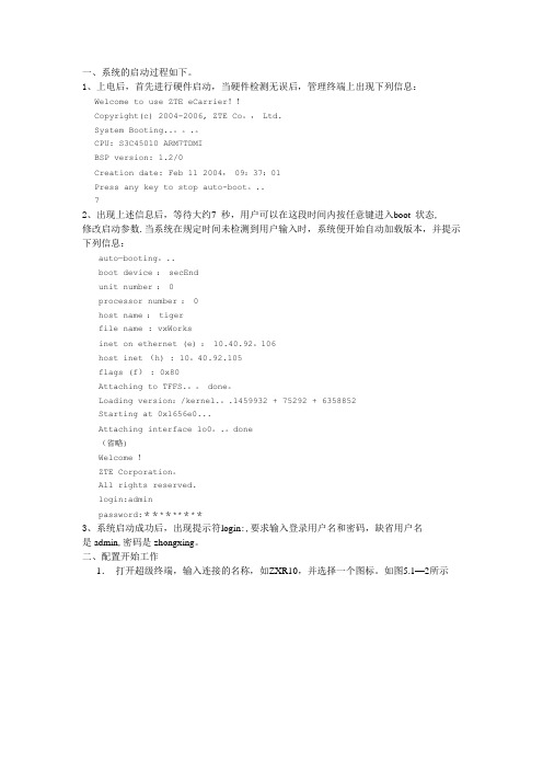
一、系统的启动过程如下。
1、上电后,首先进行硬件启动,当硬件检测无误后,管理终端上出现下列信息:Welcome to use ZTE eCarrier!!Copyright(c) 2004-2006, ZTE Co。
, Ltd.System Booting..。
.。
CPU: S3C45010 ARM7TDMIBSP version: 1.2/0Creation date: Feb 11 2004, 09:37:01Press any key to stop auto-boot。
..72、出现上述信息后,等待大约7 秒,用户可以在这段时间内按任意键进入boot 状态,修改启动参数.当系统在规定时间未检测到用户输入时,系统便开始自动加载版本,并提示下列信息:auto—booting。
..boot device : secEndunit number : 0processor number : 0host name : tigerfile name : vxWorksinet on ethernet (e) : 10.40.92。
106host inet (h) : 10。
40.92.105flags (f) : 0x80Attaching to TFFS.。
done。
Loading version:/kernel.。
.1459932 + 75292 + 6358852Starting at 0x1656e0...Attaching interface lo0。
.。
done(省略)Welcome !ZTE Corporation。
All rights reserved.login:adminpassword:*********3、系统启动成功后,出现提示符login:,要求输入登录用户名和密码,缺省用户名是admin,密码是zhongxing。
二、配置开始工作1.打开超级终端,输入连接的名称,如ZXR10,并选择一个图标。

AIX:1,获得AIX主机连接的光纤设备:# lsdev -Cc adapter -S a | grep fcsfcs0 Available 09-08 FC Adapterfcs1 Available 09-09 FC Adapter其中,显示有两块光纤卡.fcs0和fcs12,查看光纤卡的WWN号# lscfg -vpl fcs0fcs0 U787B.001.DNWG664-P1-C1-T1 FC AdapterPart Number.................10N8620Serial Number...............1B74404468Manufacturer................001BEC Level....................ACustomer Card ID Number (5759)FRU Number.................. 10N8620Device Specific.(ZM) (3)Network Address.............10000000C96E2898ROS Level and ID............02C82138Device Specific.(Z0)........1036406DDevice Specific.(Z1) (00000000)Device Specific.(Z2) (00000000)Device Specific.(Z3) (03000909)Device Specific.(Z4)........FFC01159Device Specific.(Z5)........02C82138Device Specific.(Z6)........06C12138Device Specific.(Z7)........07C12138Device Specific.(Z8)........20000000C96E2898Device Specific.(Z9)........BS2.10X8Device Specific.(ZA)........B1F2.10X8Device Specific.(ZB)........B2F2.10X8Device Specific.(ZC) (00000000)Hardware Location Code......U787B.001.DNWG664-P1-C1-T1其中标红的部分就是光纤卡的WWN号HP-Unix:1,列出HP机上连接的光纤卡设备:# ioscan -fnC fcClass I H/W Path Driver S/W State H/W Type Description=================================================================fc 0 0/3/1/0 fcd CLAIMED INTERFACE HP A6826-60001 2Gb Dual Port PCI/PCI-X Fibre Channel Adapter (FC Port 1)/dev/fcd0fc 1 0/3/1/1 fcd CLAIMED INTERFACE HP A6826-60001 2Gb Dual Port PCI/PCI-X Fibre Channel Adapter (FC Port 2)/dev/fcd1由此图可以看到,/dev/fcd0和/dev/fcd1是两个光纤卡2, 查看光纤卡的WWN号# fcmsutil /dev/fcd0Vendor ID is = 0x001077Device ID is = 0x002312PCI Sub-system Vendor ID is = 0x00103cPCI Sub-system ID is = 0x0012baPCI Mode = PCI-X 133 MHzISP Code version = 3.3.18ISP Chip version = 3Topology = PTTOPT_FABRICLink Speed = 2GbLocal N_Port_id is = 0xa10500Previous N_Port_id is = NoneN_Port Node World Wide Name = 0x50060b00001db241N_Port Port World Wide Name = 0x50060b00001db240Switch Port World Wide Name = 0x205e000dec0e2e00Switch Node World Wide Name = 0x2001000dec0e2e01Driver state = ONLINEHardware Path is = 0/3/1/0Maximum Frame Size = 2048Driver-Firmware Dump Available = NODriver-Firmware Dump Timestamp = N/ADriver Version = @(#) libfcd.a HP Fibre Channel ISP 23xx & 24xx Driver B.11.23.04 /ux/core/isu/FCD/kern/src/common/wsio/fcd_init.c:Oct 18 2005,08:21:11其中红色部分显示了HBA卡的WWNN和WWPN号,另外还能看到该HBA卡连接的光纤交换机端口的WWN号Solaris:solaris上用luxadm命令来管理存储设备以及光纤相关设备.1, 查询现有存储设备和光纤设备,可以读到包括磁盘设备的WWN号# luxadm probe2, 查看HBA的prot,可以得到HBA卡的port值以及连接属性:# luxadm -e port/devices/pci@0,0/pci1022,7450@2/pci1077,101@1/fp@0,0:devctl NOT CONNECTED/devices/pci@0,0/pci1022,7450@2/pci1077,101@1,1/fp@0,0:devctl CONNECTED从中可以看到仅有一块光纤卡连接到存储设备3, 选择那个已经连接的HBA卡,查看其WWN号格式: # luxadm -e dump_map 设备port.其中port值可从步骤2得到.如下图啊所示:# luxadm -e dump_map /devices/pci@0,0/pci1022,7450@2/pci1077,101@1/fp@0,0:devctl Pos Port_ID Hard_Addr Port WWN Node WWN Type0 0 0 210000e08b19827a 200000e08b19827a 0x1f (Unknown Type,Host Bus Adapter)Redhat:在Redhat中,设备管理的相关信息都保存在内核中,即/proc目录.所以我们一般查询CPU,内存,磁盘等信息,也是在该目录下. 其中HBA卡相关信息保存在/proc/scsi/qla2300/目录下,不同设备对应不同的文件名,例如# grep scsi /proc/scsi/qla2300/1Number of reqs in pending_q= 0, retry_q= 0, done_q= 0, scsi_retry_q= 0scsi-qla0-adapter-node=200000e08b9cf661;scsi-qla0-adapter-port=210000e08b9cf661;就可以查到系统第一块HBA卡的WWNN和WWPN号.SUSE 下查HBA卡WWN号信息∙在SUSE9下:cat /proc/scsi/qla2xxx/1这个1可能是0,或者2,3等在SUSE10下:∙cat /sys/class/fc_host/host1/node_name有时会是host2或者host3在SUSE9下:cat /proc/scsi/qla2xxx/1这个1可能是0,或者2,3等在SUSE10下:cat /sys/class/fc_host/host1/node_name有时会是host2或者host3。

N-Channel MOSFETs: OptiMOS™ (20V…250V) Product TypeProduct TypeBSN045NE2LSBSN011NE2LSBSN011NE2LSIBSN012N03LSBSN012N03LSIBSN048N03LSBSB012NE2LXBSB014N04LX3 GBSB015N04NX3 GBSB017N03LX3 GBSB012N03LX3 GBSB028N06NN3 GBSB044N08NN3 GBSB056N10NN3 GBSB013NE2LXIBSB008NE2LXBSB280N15NZ3 G BSB165N15NZ3 G BSB012NE2LXI BSF024N03LT3 G BSF050N03LQ3 G BSF030NE2LQ BSF134N10NJ3 G BSF110N06NT3 G BSF450NE7NH3 G BSF035NE2LQ IPB015N04L G IPB027N10N3 G IPB035N08N3 G IPB015N04N G IPB019N06L3 G IPB083N10N3 G IPB042N10N3 G IPB054N06N3 GIPB037N06N3 G IPB097N08N3 G IPB055N03L G IPB054N08N3 G IPB042N03L G IPB022N04L G IPB065N03L G IPB072N15N3 G IPB025N08N3 G IPB080N03L G IPB081N06L3 G IPB147N03L G IPB096N03L G IPB136N08N3 GIPB090N06N3 G IPB029N06N3 G IPB049NE7N3 G IPB031NE7N3 G IPB020NE7N3 G IPB123N10N3 G IPB038N12N3 G IPB144N12N3 G IPB320N20N3 G IPB107N20N3 G IPB200N25N3 G IPB600N25N3 G BUZ32 H3045A BUZ31 H3045A IPB108N15N3 G BUZ30A H3045AIPB107N20NA IPB057N06N IPB026N06N IPB230N06L3 G IPB067N08N3 G IPB034N03L G IPB009N03L G IPB011N04L G IPB011N04N G IPB016N06L3 G IPB017N06N3 G IPB019N08N3 G IPB020N04N G IPB025N10N3 G IPB030N08N3 GIPB036N12N3 G IPB065N15N3 G IPB010N06NIPB014N06NSPD07N20 GIPD031N06L3 G IPD034N06N3 G IPD035N06L3 G IPD036N04L GIPD038N06N3 G IPD048N06L3 G IPD053N08N3 G SPD50N03S2L-06 G SPD30N03S2L-07 G IPD068N10N3 G SPD50N03S2-07 GIPD082N10N3 G IPD088N06N3 G IPD096N08N3 G SPD30N03S2L-10 G IPD127N06L GIPD135N08N3 G IPD160N04L GIPD170N04N GIPD200N15N3 G SPD30N03S2L-20 G IPD220N06L3 G IPD25CN10N GIPD250N06N3 G IPD33CN10N GIPD350N06L GIPD640N06L G IPD78CN10N G IPD800N06N G IPD122N10N3 G IPD180N10N3 G IPD110N12N3 G IPD031N03L G IPD040N03L G IPD050N03L G IPD060N03L G IPD075N03L G IPD090N03L G IPD320N20N3 G IPD600N25N3 G IPD530N15N3 G IPD105N03L G IPD135N03L GIPD025N06N IPD053N06N IPI023NE7N3 G IPI034NE7N3 G IPI052NE7N3 G IPI126N10N3 G IPI180N10N3 G IPI041N12N3 G IPI076N12N3 G IPI147N12N3 G IPI045N10N3 G IPI086N10N3 G IPI030N10N3 G IPI04CN10N G IPI072N10N3 G IPI26CN10N G IPI35CN10N GIPI075N15N3 G IPI200N15N3 G IPI024N06N3 G IPI032N06N3 G IPI040N06N3 G IPI037N08N3 G IPI320N20N3 G IPI110N20N3 G IPI200N25N3 G IPI600N25N3 G IPI111N15N3 G IPI530N15N3 G IPI020N06NIPI029N06N BUZ31 H3046 IPI084N06L3 GIPU135N08N3 G IPS110N12N3 G IPS060N03L G IPS075N03L G IPS031N03L G IPS040N03L G IPS090N03L G IPS105N03L G IPS135N03L G IPS050N03L G BSZ0908ND BSZ0907ND BSC0921NDI BSC0923NDI BSC0924NDI BSC0925ND BSC0910NDI BSC0911NDBSZ035N03LS G BSZ035N03MS G BSZ040N04LS G BSZ042N04NS G BSZ050N03LS G BSZ050N03MS G BSZ058N03LS G BSZ058N03MS G BSZ067N06LS3 G BSZ076N06NS3 G BSZ088N03MS G BSZ088N03LS G BSZ097N04LS G BSZ100N06LS3 G BSZ100N03MS GBSZ105N04NS G BSZ110N06NS3 G BSZ123N08NS3 G BSZ130N03MS G BSZ130N03LS G BSZ165N04NS G BSZ340N08NS3 G BSZ440N10NS3 G BSZ160N10NS3 G BSZ900N15NS3 G BSZ520N15NS3 G BSZ0909NSBSZ240N12NS3 G BSZ12DN20NS3 G BSZ16DN25NS3 GBSZ42DN25NS3 G BSZ900N20NS3 G BSZ060NE2LS BSZ065N03LS BSZ036NE2LS BSZ018NE2LS BSZ0901NSBSZ0901NSIBSZ0902NSBSZ0904NSIBSZ0902NSIBSZ018NE2LSI BSZ042N06NS BSZ023N04LS BSZ150N10LS3 G BSO615N GBSO033N03MS GBSO083N03MS G BSO110N03MS G BSO330N02K G BSO150N03MD G BSO220N03MD G BSC010NE2LS BSC050NE2LS BSC046N02KS G BSC019N02KS G BSC014N03LS G BSC016N03LS G BSC014N03MS G BSC016N04LS G BSC016N03MS G BSC017N04NS G BSC018N04LS GBSC020N03MS G BSC020N03LS G BSC025N03MS G BSC027N04LS G BSC025N03LS G BSC028N06LS3 G BSC030N03MS G BSC030N04NS G BSC030N03LS G BSC031N06NS3 G BSC034N03LS G BSC035N04LS G BSC042N03MS G BSC042N03LS GBSC050N03MS G BSC050N04LS G BSC050N03LS G BSC054N04NS G BSC057N03MS G BSC057N03LS G BSC057N08NS3 G BSC059N04LS G BSC060N10NS3 G BSC067N06LS3 G BSC076N06NS3 G BSC079N10NS GBSC080N03LS G BSC082N10LS G BSC090N03MS G BSC090N03LS G BSC093N04LS G BSC100N03MS G BSC100N10NSF G BSC100N06LS3 G BSC105N10LSF G BSC110N06NS3 G BSC118N10NS G BSC120N03MS G BSC120N03LS GBSC123N10LS G BSC152N10NSF G BSC190N15NS3 G BSC159N10LSF G BSC196N10NS G BSC205N10LS G BSC252N10NSF G BSC265N10LSF G BSC340N08NS3 G BSC042NE7NS3 G BSC160N10NS3 G BSC440N10NS3 G BSC077N12NS3 G BSC190N12NS3 G BSC520N15NS3 GBSC600N25NS3 G BSC026N02KS G BSC070N10NS3 G BSC109N10NS3 G BSC0909NSBSC360N15NS3 G BSC0908NSBSC240N12NS3 G BSC900N20NS3 G BSC12DN20NS3 G BSC16DN25NS3 G BSC22DN20NS3 G BSC018NE2LS BSC024NE2LS BSC011N03LS BSC052N03LSBSC0902NSBSC032NE2LS BSC0901NSIBSC0904NSIBSC010NE2LSI BSC0902NSIBSC014NE2LSI BSC018NE2LSI BSC011N03LSI BSC0906NSBSC009NE2LS BSC036NE7NS3 G BSC046N10NS3 G BSC028N06NS BSC010N04LSI BSC014N04LS BSC014N04LSIBSC039N06NS BSC014N06NS BSC010N04LS BSC500N20NS3 G BSC022N04LS BSC072N03LD G BSC150N03LD G BSC750N10ND G IPP023NE7N3 G IPP034NE7N3 G IPP052NE7N3 G BUZ31L HBUZ73 HBUZ73A HBUZ73AL HBUZ73L HIPP180N10N3 G IPP041N12N3 G IPP048N12N3 G IPP076N12N3 G IPP114N12N3 G IPP147N12N3 G IPP030N10N3 G IPP045N10N3 G IPP04CN10N G IPP05CN10N G IPP072N10N3 G IPP086N10N3 G IPP12CN10L G IPP16CN10N G IPP075N15N3 G IPP200N15N3 G IPP034N03L GIPP055N03L G IPP065N03L G IPP080N03L G IPP096N03L G IPP114N03L G IPP015N04N G IPP023N04N G IPP039N04L G IPP041N04N G IPP024N06N3 G IPP032N06N3 G IPP037N06L3 G IPP040N06N3 G IPP052N06L3 G IPP057N06N3 G IPP084N06L3 G IPP093N06N3 GIPP028N08N3 G IPP037N08N3 G IPP057N08N3 G IPP070N08N3 G IPP100N08N3 G IPP139N08N3 G IPP320N20N3 G IPP110N20N3 G IPP200N25N3 G IPP600N25N3 G BUZ31 HBUZ32 HIPP111N15N3 G BUZ30A HIPP065N04N G IPP530N15N3 GIPP048N04N G IPP110N20NA IPP147N03L G IPP029N06N IPP020N06N IPP040N06N IPP060N06N IPA028N08N3 G IPA037N08N3 G IPA057N08N3 G IPA100N08N3 G IPA045N10N3 G IPA086N10N3 G IPA126N10N3 G IPA180N10N3 G IPA030N10N3 GIPA105N15N3 G IPA032N06N3 G IPA057N06N3 G IPA093N06N3 G IPT004N03L IPT007N06N IPT020N10N3 IPT059N15N3Datasheet Group Product Status /dgdl/BSN045NE2LS_rev1.0.pdf?fBlade 3x3 (USON-6)in production olderId=db3a304313b8b5a60113cee8763b02d7&fileId=db3a30433d68e984013d7ca959855780/dgdl/BSN011NE2LS_rev1.3.pdf?fBlade 3x3 (USON-6)in production olderId=db3a304313b8b5a60113cee8763b02d7&fileId=db3a30433d68e984013d7cbfeef05815Blade 3x3 (USON-6)in production /dgdl/BSN011NE2LSI_rev1.3.pdf?folderId=db3a304313b8b5a60113cee8763b02d7&fileId=db3a30433d68e984013d7ccf22ee58e4Blade 3x3 (USON-6)in production /dgdl/BSN012N03LS_rev1.3.pdf?folderId=db3a304313b8b5a60113cee8763b02d7&fileId=db3a30433d68e984013d7cde510c594c/dgdl/BSN012N03LSI_rev1.3.pdf?Blade 3x3 (USON-6)in production folderId=db3a304313b8b5a60113cee8763b02d7&fileId=db3a30433d68e984013d7cea5f8559f4Blade 3x3 (USON-6)in production /dgdl/BSN048N03LS_rev1.0.pdf?folderId=db3a304313b8b5a60113cee8763b02d7&fileId=db3a30433d68e984013d7cf6d2e25a60/dgdl/BSB012NE2LX_Rev+2.3.pdfCanPAK™ M-size in production?folderId=db3a304326dfb1300126fb3bec803f1a&fileId=db3a304326dfb1300126fb6a32613f3dCanPAK™ M-size in production /dgdl/BSB014N04LX3+G_Rev+2.3.pdf?folderId=db3a304313b8b5a60113cee8763b02d7&fileId=db3a304320d39d590121a02c6c737a9bCanPAK™ M-size in production /dgdl/BSB015N04NX3+G_Rev+2.4.pdf?folderId=db3a304313b8b5a60113cee8763b02d7&fileId=db3a304320d39d590121a03bbfcd7aacCanPAK™ M-size in production /dgdl/BSB017N03LX3+G_Rev+2.2.pdf?folderId=db3a304313b8b5a60113cee8763b02d7&fileId=db3a304320d39d590121a04b132c7abb/dgdl/BSB012N03LX3+G_Rev_+2CanPAK™ M-size in production.1_pdf.pdf?folderId=db3a304313b8b5a60113cee8763b02d7&fileId=db3a304320d39d590121a0112ce07a8b/dgdl/BSB028N06NN3_G_rev2.0.CanPAK™ M-size in production pdf?folderId=db3a30431441fb5d01148ca9f1be0e77&fileId=db3a30432e25b009012e29fda4e23838/dgdl/BSB044N08NN3_G_rev2.0.CanPAK™ M-size in production pdf?folderId=db3a304313b8b5a60113cee8763b02d7&fileId=db3a30435819ae2e012e385cde7b70d4CanPAK™ M-size in production /dgdl/BSB056N10NN3+G_Rev+2.5.pdf?folderId=db3a304313b8b5a60113cee8763b02d7&fileId=db3a30442e152e91012e390b9a631459/dgdl/BSB013NE2LXI_Rev+2.3.pdCanPAK™ M-size in production f?folderId=db3a304313b8b5a60113cee8763b02d7&fileId=db3a30432e398416012e47a158802577/dgdl/BSB008NE2LX_Rev+1.3.pdfCanPAK™ M-size in production?folderId=db3a304313b8b5a60113cee8763b02d7&fileId=db3a30432e564707012e5745ca7d000eCanPAK™ M-size in production /dgdl/BSB280N15NZ3+G+Rev+2.5_.pdf?folderId=db3a304326623792012669f6bee2224b&fileId=db3a30432e779412012e7b0b544c3852CanPAK™ M-size in production /dgdl/BSB165N15NZ3+G+Rev+2.2.pdf?folderId=db3a304326623792012669f6bee2224b&fileId=db3a30432e779412012e7b04a1353843/dgdl/BSB012NE2LXI_rev1+1.pdfCanPAK™ M-size coming soon?folderId=db3a304313b8b5a60113cee8763b02d7&fileId=db3a30433f764301013f805e3eb247c1CanPAK™ S-size in production /dgdl/BSF024N03LT3+G_Rev+2.1_pdf.pdf?folderId=db3a30431ddc9372011ebafa04517f8b&fileId=db3a30432239cccd012282adaadf7bc8CanPAK™ S-size in production /dgdl/BSF050N03LQ3+G_Rev+2.2.pdf?folderId=db3a304313b8b5a60113cee8763b02d7&fileId=db3a304320d39d590121a0f584407b1cCanPAK™ S-size in production /dgdl/BSF030NE2LQ_Rev+2.3.pdf?folderId=db3a304313b8b5a60113cee8763b02d7&fileId=db3a30432e398416012e47a8f0792588/dgdl/BSF134N10NJ3+G_Rev+2.5CanPAK™ S-size in production.pdf?folderId=db3a304313b8b5a60113cee8763b02d7&fileId=db3a30432e779412012e7afa4a6c3834CanPAK™ S-size in production /dgdl/BSF110N06NT3_G_rev2.0.pdf?folderId=db3a304313b8b5a60113cee8763b02d7&fileId=db3a3043382e837301387b92fdc80c37CanPAK™ S-size in production /dgdl/BSF450NE7NH3G_rev2.0.pdf?folderId=db3a304313b8b5a60113cee8763b02d7&fileId=db3a30433a047ba0013a687e2ae403daCanPAK™ S-size coming soon /dgdl/BSF035NE2LQ_rev1+1.pdf?folderId=db3a304313b8b5a60113cee8763b02d7&fileId=db3a30433f764301013f7fe8a925463cD2PAK (TO-263)in production /dgdl/IPB015N04L_rev1.2.pdf?folderId=db3a304313b8b5a60113cee8763b02d7&fileId=db3a30431936bc4b0119382488c359d3D2PAK (TO-263)in production /dgdl/IPB027N10N3+G_Rev2.4.pdf?folderId=db3a304313b8b5a60113cee8763b02d7&fileId=db3a30431ce5fb52011d1ed9348e15efD2PAK (TO-263)in production /dgdl/IPP037N08N3_Rev2.3.pdf?folderId=db3a304313b8b5a60113cee8763b02d7&fileId=db3a30431add1d95011ae8426111565bD2PAK (TO-263)in production /dgdl/IPB015N04N_rev2.2.pdf?folderId=db3a3043156fd5730115c7d50620107c&fileId=db3a30431689f4420116c474de8f0845/dgdl/IPB019N06L3_Rev2.2.pdf?fD2PAK (TO-263)in production olderId=db3a30431441fb5d01148ca9f1be0e77&fileId=db3a30431ddc9372011e2600a49e467b/dgdl/IPP086N10N3+G_Rev2.5.pdD2PAK (TO-263)in productionf?folderId=db3a304313b8b5a60113cee8763b02d7&fileId=db3a30431ce5fb52011d1ac5c8fa1358/dgdl/IPP045N10N3+G_Rev2.5.pdD2PAK (TO-263)in productionf?folderId=db3a304313b8b5a60113cee8763b02d7&fileId=db3a30431ce5fb52011d1e8b0cc31586D2PAK (TO-263)not for new design /dgdl/IPP_B057N06N3_Rev2.2.pdf?folderId=db3a30431441fb5d01148ca9f1be0e77&fileId=db3a30431ddc9372011e2b439f1d4d93/dgdl/IPP037N06L3_Rev2.7.pdf?fD2PAK (TO-263)in production olderId=db3a304313b8b5a60113cee8763b02d7&fileId=db3a30431b3e89eb011b4561341f7d38D2PAK (TO-263)in production /dgdl/IPP040N06N3_Rev1.03.pdf?folderId=db3a3043163797a6011637c252b10018&fileId=db3a304317a7483601182c2d4f447647D2PAK (TO-263)in production /dgdl/IPP_I_B100N08N3_Rev2.2.pdf?folderId=db3a304313b8b5a60113cee8763b02d7&fileId=db3a30431ddc9372011e071f53b82619D2PAK (TO-263)in production /dgdl/IPP055N03L_rev2.0.pdf?folderId=db3a30431441fb5d01148c401f250e27&fileId=db3a30431441fb5d01148d01ee1c0e91/dgdl/IPP057N08N3_Rev1.2.pdf?fD2PAK (TO-263)in production olderId=db3a304313b8b5a60113cee8763b02d7&fileId=db3a304317a748360117cf0cf5951d06/dgdl/IPP042N03L_rev2.0.pdf?foldD2PAK (TO-263)in production erId=db3a30431441fb5d01148c401f250e27&fileId=db3a30431441fb5d01148d012d010e8eD2PAK (TO-263)discontinued /dgdl/IPB022N04L_rev2.0.pdf?folderId=db3a304313b8b5a60113cee8763b02d7&fileId=db3a30431936bc4b01193836c99c5a08D2PAK (TO-263)in production /dgdl/IPP065N03L_rev2.0.pdf?folderId=db3a30431441fb5d01148c401f250e27&fileId=db3a30431441fb5d011492371ebc0fe2/dgdl/IPP075N15N3+G_Rev2.06.pD2PAK (TO-263)in production df?folderId=db3a304313b8b5a60113cee7c66a02d6&fileId=db3a304319c6f18c0119cd76cc527ab6/dgdl/IPB025N08N3_Rev1.2.pdf?fD2PAK (TO-263)in production olderId=db3a304313b8b5a60113cee8763b02d7&fileId=db3a304317a748360117d35658bc066bD2PAK (TO-263)in production /dgdl/IPP080N03L_rev2.0.pdf?folderId=db3a30431441fb5d01148c401f250e27&fileId=db3a30431441fb5d01148d028c300e94D2PAK (TO-263)in production /dgdl/IPP_B084N06L3_Rev2.23.pdf?folderId=db3a304313b8b5a60113cee8763b02d7&fileId=db3a30431b3e89eb011b4592273f7db2/dgdl/IPP147N03L_rev2.0.pdf?foldD2PAK (TO-263)in production erId=db3a30431441fb5d01148c401f250e27&fileId=db3a30431441fb5d01148d08f1f30e9aD2PAK (TO-263)in production /dgdl/IPP096N03L_rev2.0.pdf?folderId=db3a30431441fb5d01148c401f250e27&fileId=db3a30431441fb5d01148d0849910e97/dgdl/IPP139N08N3_Rev2.5.pdf?fD2PAK (TO-263)in production olderId=db3a304313b8b5a60113cee8763b02d7&fileId=db3a30431add1d95011ae8a77e3656c2?folderId=db3a304313b8b5a60113cee7c66a02d6&fileId=db3a304319c6f18c0119cd1cc23279beD2PAK (TO-263)in production /dgdl/IPP_B093N06N3_Rev1.2.pdf?folderId=db3a3043163797a6011637c252b10018&fileId=db3a304317a7483601182c3043a67656D2PAK (TO-263)in production /dgdl/IPP032N06N3_Rev2.2.pdf?folderId=db3a30431441fb5d01148ca9f1be0e77&fileId=db3a30431ddc9372011e2a84ff084cc8/dgdl/IPB049NE7N3_Rev2.2.pdf?fD2PAK (TO-263)in production olderId=db3a304313b8b5a60113cee8763b02d7&fileId=db3a304320d39d590121a517a48e0bb9D2PAK (TO-263)in production /dgdl/IPB031NE7N3_Rev2.2.pdf?folderId=db3a304313b8b5a60113cee8763b02d7&fileId=db3a304320d39d590121a52a87680bc8/dgdl/IPB020NE7N3_Rev2.2.pdf?fD2PAK (TO-263)in production olderId=db3a304313b8b5a60113cee8763b02d7&fileId=db3a304320d39d590121e31c838554d3D2PAK (TO-263)in production /dgdl/IPP126N10N3+G_Rev2.3.pdf?folderId=db3a304313b8b5a60113cee8763b02d7&fileId=db3a30432239cccd012260508e027f74D2PAK (TO-263)in production /dgdl/IPP_I_B041N12N3_Rev2.2.pdf?folderId=db3a304313b8b5a60113cee8763b02d7&fileId=db3a30432239cccd0122a75b86467ca4D2PAK (TO-263)in production /dgdl/IPP_I_B147N12N3+G_Rev2.6.pdf?folderId=db3a304313b8b5a60113cee8763b02d7&fileId=db3a30432239cccd0122a79a30f57d01D2PAK (TO-263)in production /dgdl/IPP_B_I_320N20N3+G+Rev2.3.pdf?folderId=db3a3043163797a6011637d4bae7003b&fileId=db3a3043243b5f170124967064ba184aD2PAK (TO-263)in production /dgdl/IPP_I_110N20N3+G_IPB107N20N3+G+Rev2.3.pdf?folderId=db3a3043163797a6011637d4bae7003b&fileId=db3a3043243b5f170124968e7d1f18e7/dgdl/IPP_B_I_200N25N3+G+RevD2PAK (TO-263)in production2.4.pdf?folderId=db3a3043163797a6011637d4bae7003b&fileId=db3a3043243b5f17012496b87e9f1971/dgdl/IPP_B_600N25N3+G+Rev2.D2PAK (TO-263)in production3.pdf?folderId=db3a3043163797a6011637d4bae7003b&fileId=db3a3043243b5f17012496c9548d199cD2PAK (TO-263)not for new design /dgdl/BUZ32+H3045A+rev+2.2.pdf?folderId=db3a304325305e6d012596c6ca7b290a&fileId=db3a304325305e6d01259718c8d8291eD2PAK (TO-263)not for new design /dgdl/BUZ31+H3045+A+Rev+2.1.pdf?folderId=db3a304325305e6d012596c6ca7b290a&fileId=db3a304325305e6d0125971c90292922D2PAK (TO-263)in production /dgdl/IPP_I111N15N3+G_IPB108N15N3+G_Rev2.1.pdf?folderId=db3a304325305e6d01254a567c041b4e&fileId=db3a304325305e6d01254a5795541b4fD2PAK (TO-263)in production /dgdl/Buz30a+H3045A+Rev+2.2.pdf?folderId=db3a304325305e6d012596c6ca7b290a&fileId=db3a304325305e6d012596cd45e4290folderId=db3a304326623792012669f6bee2224b&fileId=db3a30432662379201266a1f6dd2227c/dgdl/IPP110N20NA_IPB107N20NA+Rev2.1.pdf?folderId=db3a304325305e6d012596c6ca7b290a&fileId=db3a3043300464130130307ce52a20a3D2PAK (TO-263)in production/dgdl/IPB057N06N_Rev2.2.pdf?folderId=db3a304313b8b5a60113cee8763b02d7&fileId=db3a30433727a44301372c2ed50b49b3D2PAK (TO-263)in production/dgdl/IPB026N06N_Rev2.2.pdf?folderId=db3a304313b8b5a60113cee8763b02d7&fileId=db3a3043372d5cc8013754c7b2a74f7cD2PAK (TO-263)in production/dgdl/IPP_B230N06L3_Rev2.2_.pdf?folderId=db3a30431441fb5d01148ca9f1be0e77&fileId=db3a30431ddc9372011e2aab4a564d14D2PAK (TO-263)discontinued/dgdl/IPP070N08N3_Rev2.3.pdf?folderId=db3a304313b8b5a60113cee8763b02d7&fileId=db3a30431add1d95011ae849e8f1566bD2PAK (TO-263)in production/dgdl/IPP034N03L_rev2.0.pdf?folderId=db3a304313b8b5a60113cee8ed2a02db&fileId=db3a304313b8b5a60113d3c9730503e7D2PAK (TO-263)in production/dgdl/IPB009N03L_rev1.3.pdf?fold erId=db3a3043156fd5730115c7d50620107c&fileId=db3a3 0431689f4420116d426b6770ca3D2PAK 7pin (TO-2637pin)in production/dgdl/IPB011N04L_rev1.3.pdf?fold erId=db3a3043156fd5730115c7d50620107c&fileId=db3a3 0431689f4420116c451f4e20825D2PAK 7pin (TO-2637pin)in production/dgdl/IPB011N04N_rev1+4.pdf?fol derId=db3a3043163797a6011643468e7505a4&fileId=db3 a3043163797a601164373e07005f8D2PAK 7pin (TO-2637pin)in production/dgdl/IPB016N06L3_Rev2.3.pdf?f olderId=db3a30431441fb5d01148ca9f1be0e77&fileId=db3 a30431ddc9372011e261543e54693D2PAK 7pin (TO-2637pin)in production/dgdl/IPB017N06N3_Rev2.2.pdf?f olderId=db3a30431441fb5d01148ca9f1be0e77&fileId=db3 a30431ddc9372011e264a7ab746ea D2PAK 7pin (TO-2637pin)in production/dgdl/IPB019N08N3_Rev2.3.pdf?f olderId=db3a304313b8b5a60113cee8763b02d7&fileId=db 3a30431add1d95011ae87fdf90569f D2PAK 7pin (TO-2637pin)in production/dgdl/IPB020N04N_rev1.3.pdf?fol derId=db3a304313b8b5a60113cee8763b02d7&fileId=db3 a30431936bc4b0119382c70a859ed D2PAK 7pin (TO-2637pin)in production/dgdl/IPB025N10N3+G_Rev2.03.p df?folderId=db3a304313b8b5a60113cee8763b02d7&fileId =db3a30431ce5fb52011d1ab1d9d51349D2PAK 7pin (TO-2637pin)in production/dgdl/IPB030N08N3_Rev2.3.pdf?f olderId=db3a304313b8b5a60113cee8763b02d7&fileId=db 3a30431add1d95011ae88a47a856b1D2PAK 7pin (TO-2637pin)in productiondf?folderId=db3a304313b8b5a60113cee8763b02d7&fileId=db3a30431ce5fb52011d1ed1fd3915e07pin)/dgdl/IPB036N12N3+G_Rev2.2.pd f?folderId=db3a304313b8b5a60113cee8763b02d7&fileId= db3a304323b87bc20123c7030ed51f56D2PAK 7pin (TO-2637pin)in production/dgdl/IPB065N15N3+G_Rev2.1.pd f?folderId=db3a304326623792012669f6bee2224b&fileId= db3a30432662379201266a0379d1225c D2PAK 7pin (TO-2637pin)in production/dgdl/IPB010N06N_Rev2.1.pdf?fol derId=db3a304313b8b5a60113cee8763b02d7&fileId=db3 a3043353fdc1601355341f17a485f D2PAK 7pin (TO-2637pin)in production/dgdl/IPB014N06N_Rev2.2.pdf?fol derId=db3a304313b8b5a60113cee8763b02d7&fileId=db3 a3043353fdc160135534e951e4873D2PAK 7pin (TO-2637pin)in production/dgdl/spd07n20_Rev+2.5.pdf?folderId=db3a30431a5c32f2011a809773886508&fileId=db3a30431f848401011fc73c3e60796aDPAK (TO-252)in production/dgdl/IPD031N06L3_Rev2.0.pdf?folderId=db3a30431441fb5d01148ca9f1be0e77&fileId=db3a30431ddc9372011e2a9f6a9d4d02DPAK (TO-252)in production/dgdl/IPD034N06N3_Rev2.0.pdf?folderId=db3a30431441fb5d01148ca9f1be0e77&fileId=db3a30431ddc9372011e2a97343b4cf3DPAK (TO-252)in production/dgdl/IPD035N06L3_Rev2.3.pdf?folderId=db3a304313b8b5a60113cee8763b02d7&fileId=db3a30431b3e89eb011b4558ed7f7d14DPAK (TO-252)in production/dgdl/IPD036N04L_rev1.0.pdf?folderId=db3a3043163797a6011643468e7505a4&fileId=db3a3043163797a6011643476a6505a5DPAK (TO-252)in production/dgdl/IPD038N06N3_Rev1.02.pdf?folderId=db3a3043132679fb0113346bdc4505a3&fileId=db3a304317a7483601181bf8dae11675DPAK (TO-252)in production/dgdl/IPD048N06L3_Rev2.0.pdf?folderId=db3a30431441fb5d01148ca9f1be0e77&fileId=db3a30431ddc9372011e2b4f496e4db0DPAK (TO-252)in production/dgdl/IPD053N08N3_Rev1.0.pdf?folderId=db3a304313b8b5a60113cee8763b02d7&fileId=db3a304317a748360117cf072cf31ce8DPAK (TO-252)in production/dgdl/SPD50N03S2L-06+rev+1.2.pdf?folderId=db3a304313b8b5a60113cee8763b02d7&fileId=db3a30431b3e89eb011b9718a1a20e3cDPAK (TO-252)in production/dgdl/SPD30N03S2L-07+rev+1.2.pdf?folderId=db3a304313b8b5a60113cee8763b02d7&fileId=db3a30431b3e89eb011b92c6dcba0f89DPAK (TO-252)in production/dgdl/IPD068N10N3+G_Rev2.1.pdf?folderId=db3a304313b8b5a60113cee8763b02d7&fileId=db3a30431ce5fb52011d1eb7aeb615d1DPAK (TO-252)in production/dgdl/SPD50N03S2-07+rev+1.2.pdf?folderId=db3a304313b8b5a60113cee8763b02d7&fileId=db3a30431b3e89eb011b97117df80e2aDPAK (TO-252)in productionolderId=db3a30431441fb5d01148ca9f1be0e77&fileId=db3a30431ddc9372011e2b5528634dc0DPAK (TO-252)in production /dgdl/IPP086N10N3+G_Rev2.5.pdf?folderId=db3a304313b8b5a60113cee8763b02d7&fileId=db3a30431ce5fb52011d1ac5c8fa1358DPAK (TO-252)in production /dgdl/IPD088N06N3_Rev2.0.pdf?folderId=db3a30431441fb5d01148ca9f1be0e77&fileId=db3a30431ddc9372011e2b2351db4d5c/dgdl/IPD096N08N3_Rev2+1.pdf?DPAK (TO-252)in production folderId=db3a304313b8b5a60113cee8763b02d7&fileId=db3a30431ce5fb52011d1f35150315feDPAK (TO-252)in production /dgdl/SPD30N03S2L-10+rev+1.2.pdf?folderId=db3a304313b8b5a60113cee8763b02d7&fileId=db3a30431b3e89eb011b96e752ea0e08/dgdl/IPD127N06LG%2BRev1.2.pDPAK (TO-252)not for new design df?folderId=db3a30431a5c32f2011a809773886508&fileId=db3a30431f848401011fc786d4077a24DPAK (TO-252)in production /dgdl/IPD135N08N3_Rev2.1.pdf?folderId=db3a304313b8b5a60113cee8763b02d7&fileId=db3a30431add1d95011ae8b1143256d4/dgdl/IPD160N04L_rev1.0.pdf?folDPAK (TO-252)not for new design derId=db3a3043163797a6011643468e7505a4&fileId=db3a3043163797a60116436401cf05cfDPAK (TO-252)not for new design /dgdl/IPD170N04N_rev1.0.pdf?folderId=db3a3043163797a6011643468e7505a4&fileId=db3a3043163797a601164367820f05dd/dgdl/IPD200N15N3_Rev2.05.pdfDPAK (TO-252)in production?folderId=db3a304313b8b5a60113cee7c66a02d6&fileId=db3a304319c6f18c0119cd1cc23279beDPAK (TO-252)in production /dgdl/SPD30N03S2L-20+rev+1.2.pdf?folderId=db3a304313b8b5a60113cee8763b02d7&fileId=db3a30431b3e89eb011b96f227b90e19/dgdl/IPD220N06L3_Rev2.0.pdf?fDPAK (TO-252)not for new design olderId=db3a30431441fb5d01148ca9f1be0e77&fileId=db3a30431ddc9372011e266fb35e471aDPAK (TO-252)in production /dgdl/IPP26CN10N_Rev1.08.pdf?folderId=db3a304412b407950112b408e8c90004&fileId=db3a304412b407950112b42b420244aa/dgdl/IPD250N06N3_Rev2.0.pdf?fDPAK (TO-252)not for new design olderId=db3a30431441fb5d01148ca9f1be0e77&fileId=db3a30431ddc9372011e268ceca1474fDPAK (TO-252)in production /dgdl/IPP35CN10N_Rev1.09.pdf?folderId=db3a304412b407950112b408e8c90004&fileId=db3a304412b407950112b42b457b44b1DPAK (TO-252)in production /dgdl/IPD350N06L+G++Rev1.3.pdf?folderId=db3a304313b8b5a60113cee8763b02d7&fileId=db3a30431be39b97011c320778777982?folderId=db3a304313b8b5a60113cee8763b02d7&fileId=db3a30431be39b97011c31db9a4f795cDPAK (TO-252)in production /dgdl/IPD640N06L%2BG%2BRev1.4.pdf?folderId=db3a30431ddc9372011ebafa04517f8b&fileId=db3a30431f848401011fcafb4ac00440DPAK (TO-252)in production /dgdl/IPP80CN10N_Rev1.09.pdf?folderId=db3a304412b407950112b408e8c90004&fileId=db3a304412b407950112b42c2aaf468dDPAK (TO-252)not for new design /dgdl/IPD800N06N%2BG%2BRev1.3.pdf?folderId=db3a30431ddc9372011ebafa04517f8b&fileId=db3a30431f848401011fcaff7887044fDPAK (TO-252)in production /dgdl/IPD122N10N3+G_Rev2.2.pdf?folderId=db3a304313b8b5a60113cee8763b02d7&fileId=db3a30432239cccd0122604a0b2e7f65DPAK (TO-252)in production /dgdl/IPD180N10N3+G_Rev2.2.pdf?folderId=db3a304313b8b5a60113cee8763b02d7&fileId=db3a30432239cccd01226070a4bb7fb9DPAK (TO-252)in production /dgdl/IPD_S110N12N3+G_Rev2.2.pdf?folderId=db3a304313b8b5a60113cee8763b02d7&fileId=db3a30432239cccd0122a7a49e2b7d1dDPAK (TO-252)in production /dgdl/IPD031N03L_rev2+1.pdf?folderId=db3a304313b8b5a60113cee8763b02d7&fileId=db3a30432313ff5e01239e2ed62a6fffDPAK (TO-252)in production /dgdl/IPD040N03LG_rev1%5B1%5D.02.pdf?folderId=db3a304313b8b5a60113cee8763b02d7&fileId=db3a30432313ff5e01239e343d7c700fDPAK (TO-252)in production /dgdl/IPD050N03LG_rev1%5B1%5D.02.pdf?folderId=db3a304313b8b5a60113cee8763b02d7&fileId=db3a30432313ff5e01239e47dbfe701f/dgdl/IPD060N03LG_rev2.0.pdf?fDPAK (TO-252)in production olderId=db3a304313b8b5a60113cee8763b02d7&fileId=db3a30432313ff5e01239e4d33a3702f/dgdl/IPD075N03LG_rev1%5B1%DPAK (TO-252)in production5D.1.pdf?folderId=db3a304313b8b5a60113cee8763b02d7&fileId=db3a30432313ff5e01239e56990c7047/dgdl/IPD090N03LG_rev2.0_.pdf?DPAK (TO-252)in production folderId=db3a304313b8b5a60113cee8763b02d7&fileId=db3a30432313ff5e01239eac54cb707bDPAK (TO-252)in production /dgdl/IPD320N20N3+G+Rev2.3.pdf?folderId=db3a3043163797a6011637d4bae7003b&fileId=db3a3043243b5f1701249669796017f3/dgdl/IPD600N25N3+G+Rev2.3.pDPAK (TO-252)in productiondf?folderId=db3a3043163797a6011637d4bae7003b&fileId=db3a3043243b5f17012496b03c67195bDPAK (TO-252)in production /dgdl/IPD530N15N3_Rev2.5.pdf?folderId=db3a304326623792012669f6bee2224b&fileId=db3a30432662379201266a1f6dd2227c/dgdl/IPD105N03LG_rev2.1.pdf?fDPAK (TO-252)in production olderId=db3a304313b8b5a60113cee8ed2a02db&fileId=db3a3043271faefd0127b84794a33348/dgdl/IPD135N03LG_rev2.1.pdf?fDPAK (TO-252)in production olderId=db3a304313b8b5a60113cee8ed2a02db&fileId=db3a304327b897500127b8b9540f0003DPAK (TO-252)not for new design /dgdl/IPP12CN10N_Rev1.07.pdf?folderId=db3a304412b407950112b408e8c90004&fileId=db3a304412b407950112b42c236e467cDPAK (TO-252)in production /dgdl/IPD025N06N_Rev2.3.pdf?folderId=db3a304313b8b5a60113cee8763b02d7&fileId=db3a304336415dec0136531648062c76/dgdl/IPD053N06N_Rev2.2.pdf?foDPAK (TO-252)in production lderId=db3a304313b8b5a60113cee8763b02d7&fileId=db3a30433727a44301372c22c4c3499fI2PAK (TO-262)in production /dgdl/IPP_I023NE7N3_Rev2+11.pdf?folderId=db3a304313b8b5a60113cee8763b02d7&fileId=db3a304320d39d5901210a9da8c22702I2PAK (TO-262)in production /dgdl/IPP_I034NE7N3_Rev2+01.pdf?folderId=db3a304313b8b5a60113cee8763b02d7&fileId=db3a304320d39d5901210ab6d74b2720I2PAK (TO-262)in production /dgdl/IPP_I052NE7N3_Rev2+01.pdf?folderId=db3a304313b8b5a60113cee8763b02d7&fileId=db3a304320d39d5901210ac80a8c273d/dgdl/IPP126N10N3+G_Rev2.3.pdI2PAK (TO-262)in productionf?folderId=db3a304313b8b5a60113cee8763b02d7&fileId=db3a30432239cccd012260508e027f74I2PAK (TO-262)in production /dgdl/IPP180N10N3+G+Rev2.2.pdf?folderId=db3a304313b8b5a60113cee8763b02d7&fileId=db3a30432239cccd01226066faa07f9dI2PAK (TO-262)in production /dgdl/IPP_I_B041N12N3_Rev2.2.pdf?folderId=db3a304313b8b5a60113cee8763b02d7&fileId=db3a30432239cccd0122a75b86467ca4I2PAK (TO-262)in production /dgdl/IPP_I076N12N3+G_Rev2.3.pdf?folderId=db3a304313b8b5a60113cee8763b02d7&fileId=db3a30432239cccd0122a77a83ab7cd4I2PAK (TO-262)in production /dgdl/IPP_I_B147N12N3+G_Rev2.6.pdf?folderId=db3a304313b8b5a60113cee8763b02d7&fileId=db3a30432239cccd0122a79a30f57d01I2PAK (TO-262)in production /dgdl/IPP045N10N3+G_Rev2.5.pdf?folderId=db3a304313b8b5a60113cee8763b02d7&fileId=db3a30431ce5fb52011d1e8b0cc31586I2PAK (TO-262)in production /dgdl/IPP086N10N3+G_Rev2.5.pdf?folderId=db3a304313b8b5a60113cee8763b02d7&fileId=db3a30431ce5fb52011d1ac5c8fa1358I2PAK (TO-262)in production /dgdl/IPP030N10N3+G_Rev2%5B1%5D.1.pdf?folderId=db3a304313b8b5a60113cee8763b02d7&fileId=db3a30432313ff5e0123939fdbcf03c9/dgdl/IPP04CN10N_Rev1.4.pdf?foI2PAK (TO-262)not for new design lderId=db3a304313b8b5a60113cee8763b02d7&fileId=db3a30432313ff5e012393a80d1d03d8/dgdl/IPP072N10N3+G_Rev2%5BI2PAK (TO-262)in production1%5D.1.pdf?folderId=db3a304313b8b5a60113cee8763b02d7&fileId=db3a30432313ff5e012393bed2d20405/dgdl/IPP26CN10N_Rev1.08.pdf?fI2PAK (TO-262)discontinued olderId=db3a304313b8b5a60113cee8763b02d7&fileId=db3a30432313ff5e012393d285660441I2PAK (TO-262)discontinued /dgdl/IPP35CN10N_Rev1.09.pdf?folderId=db3a304313b8b5a60113cee8763b02d7&fileId=db3a304317a748360117cf1876cc1d1a。

Agilent 81689A / 81689B / 81649A Compact Tunable Laser Modules Technical SpecificationsFebruary 2002The 81689A, 81689B, 81649A compact tunable lasermodules offer superior performance now also in the compactmodule class. As they are tunable with continuous outputpower, they are the most flexible stimulus for the test ofoptical amplifiers, DWDM components as well as for the testof complete DWDM systems.Compact tunable lasers for C-and L-bandThe Agilent 81689A and 81689B modules operate in the C-band from 1525 nm to 1575 nm, whereas the Agilent 81649A covers the L-band from 1570 nm to 1620 nm.Test of optical amplifiersA variable amount of the compact, yet fully remote controlled Agilent 81689A, 81689B and 81649A tunable laser modules, in combination with the 81682A and 81642A high power Tunable Laser, is the ideal solution to characterize optical amplifiers for use in DWDM applications. The 81689A, 81689B and 81649A compact tunable laser modules provide the high stimulus power needed to test today's optical amplifiers. Together with the 81651A optical attenuator module, an output power dynamic range of more than60 dB can be achieved. Even without the attenuator module the power can be attenuated by 9dB (10dB for 81689B) e.g. to equalize power levels of several sources. Polarization Maintaining Fiber for the test of integrated optical devicesThe 81689A, 81689B and 81649A modules are ideally constructed to characterize integrated optical devices. Their optional Panda PMF output ports provide a well defined state of polarization to ensure constant measurement conditions on waveguidedevices. A PMF cable easily connectsan external optical modulator.The 81689A, 81689B and 81649A isavailable with both, standard single-mode fiber and Panda type PMF.Compact module for DWDMmulti-channel testThe 81689A, 81689B and 81489Aallow a realistic multi-channel test bedfor DWDM transmission systems to beset up.Their flexibility make them thepreferred choice for tests of DWDMtransmission system during installationand maintenance phases.Compact spare for DFBmodules in ITU gridsThe 81689B for the first time solvesthe sparing nightmare for users ofDWDM combs. In combination with acomb of 81662A DFB lasers the81689B can replace any DFB between1525nm and 1575nm without powerpenalty.Remote control & PnPsoftware drivers for easyprocess automationIts continuous, mode-hop free tuningmakes it quick and easy to set even themost complex configurations to thetarget wavelengths and power levels,just by dialing or using the vernier keys.A 8163B mainframe can host2 compact tunable laser modules. Thisallows for the most compact C- and L-band stimulus solution available today.Each 8164B mainframe can host up tofour units of the 81689A, 81689B or81649A in its upper slots.The 8166B is most interesting for highchannel count solutions. Up to17 compact tunable laser modules canbe hosted here.The 81649A, 81689A and 81689B areproduced to ISO 9001 internationalquality system standard as part ofAgilent's commitment to continuallyincreasing customer satisfactionthrough improved quality control.Specifications describe theinstrument's warranted performance.They are verified at the end of a 2 mlong patchcord and are valid afterwarm-up and for the stated outputpower and wavelength ranges.Each specification is assured bythoroughly analyzing all measurementuncertainties. Supplementaryperformance characteristics describethe instrument’s non-warranted typicalperformance.Every instrument is delivered with acommercial certificate of calibrationand a detailed test report.For further details on specifications,see the Definition of Terms in AppendixC of the Compact Tunable Laser User'sGuide.81689A, 81689B, 81649A Compact Tunable Laser for Multi-channel test applicationsAgilent 81689A Agilent 81689B Agilent 81649A Wavelength range1525 nm to 1575 nm1525 nm to 1575 nm1570 nm to 1620 nm Wavelength resolution0.01 nm, 1.25 GHz at 1550 nm0.01 nm, 1.25 GHz at 1550 nm0.01 nm, 1.17 GHz at 1595 nm Absolute wavelength accuracy (typ.) [1]±0.3 nm±0.3 nm±0.3 nmRelative wavelength accuracy [1]±0.3 nm±0.15 nm±0.15 nmWavelength repeatability [1]±0.05 nm±0.05 nm±0.05 nmWavelength stability(typ., over 24 h at constant temperature)[1] (typ., over 1 h at constant temperature)[1]±0.02 nm±0.01 nm±0.005 nm±0.01 nm±0.005 nmTuning speed (typ.)<10 sec/ 50 nm<10 sec/ 50 nm<10 sec/ 50 nmLinewidth (typ.) [2]with Coherence Control ON (typ.) [2]20 MHz---< 20MHz>100MHz< 20MHz>100MHzOutput power (continuous power on duringtuning)≥ 6 dBm (1525 –1575nm)≥ 10 dBm (1525 –1575nm)≥ 6 dBm (1570 –1620nm) Minimum output power–3 dBm0 dBm–3 dBmPower stability (at constant temperature) [3]±0.03 dB over 1 hour,typ. ±0.06 dB over 24 hours ±0.015 dB over 1 hour,typ. ±0.0075 dB over 1 hour,typ. ±0.05 dB over 24 hours±0.015 dB over 1 hour,typ. ±0.0075 dB over 1 hour,typ. ±0.05 dB over 24 hoursPower repeatability (typ.) [3]±0.02 dB±0.02 dB±0.02 dB Power linearity±0.1dB±0.1dB±0.1dB Power flatness versus wavelength±0.3 dB±0.2 dB±0.2 dBSide-mode suppression ratio (typ.) [2]> 40 dB(1525 – 1575 nm at 0 dBm)> 45 dB(1525 – 1575 nm at ≥ 3 dBm)> 45 dB(1570 – 1620 nm at ≥ 0 dBm)Signal to source spontaneous emission ratio (typ.) [4]≥ 39 dB/ nm(1525 –1575 nm at 6 dBm)≥ 44 dB/ nm(1525 –1575 nm at 10 dBm)≥ 42 dB/ nm(1570 – 1620 nm at 6 dBm)Relative intensity noise (RIN, typ.)< -137 dB/Hz(100 MHz – 2.5 GHz, at +3 dBm)< -137 dB/Hz(100 MHz – 2.5 GHz, at +7 dBm)< -137 dB/Hz(100 MHz – 2.5 GHz, at +3 dBm)Dimensions75 mm H, 32 mm W, 335 mm D(2.8" x 1.3" x 13.2")75 mm H, 32 mm W, 335 mm D(2.8" x 1.3" x 13.2")75 mm H, 32 mm W, 335 mm D(2.8" x 1.3" x 13.2")Weight 1 kg 1 kg 1 kg[1]At CW operation. Measured with wavelength meter based on wavelength in vacuum.[2]Measured by heterodyning method.[3]500 ms after changing power.[4]Measured with optical spectrum analyzer at 1 nm resolution bandwidth.Listed optionsOption 021: standard single mode fiber,straight contact output connectorOption 022: standard single mode fiber,angled contact output connectorOption 071: polarization maintainingfiber, straight contact output connectorOption 072: polarization maintainingfiber, angled contact output connectorSupplementary performance characteristics ModulationInternal digital modulation50% duty cycle, 200 Hz to 300 kHz.>45% duty cycle, 300 kHz to 1 MHz. Modulation output (via Mainframe): TTL reference signal.External digital modulation> 45% duty cycle, fall time< 300 ns, 200 Hz to 1 MHz. Modulation input (via Mainframe):TTL signal.External analog modulation≥ ±15% modulation depth,5 kHz to 1 MHz.Modulation input: 5 Vp-p Coherence control(81649A/81689B)For measurements on components with 2 m long patchcords and connectors with 14 dB return loss, the effective linewidth results in a typical power stability of< ±0.025 dB over1 minute by reducing interference effects in the test setup.GeneralOutput isolation (typ.):38 dBReturn loss (typ.):55 dB (options 022, 072)40 dB (options 021, 071)Polarization maintaining fiber (Options071, 072)Fiber type: Panda.Orientation: TE mode in slow axis,in line with connector key.Extinction ratio: 16 dB typ.Laser class:Class IIIb according to FDA 21 CFR1040.10, Class 3A according to IEC 825- 1; 1993.Recommended re-calibration period:2 years.Warm-up time:< 40 min,immediate operation after boot-up.EnvironmentalStorage temperature:–20 °C to +70 °C (81689A)–40 °C to +70 °C (81689B, 81649A)Operating temperature:15 °C to 35 °CHumidity:< 80 % R.H. at 15 °C to 35 °CSpecifications are valid in non-condensingconditions.Laser Safety InformationAll laser sources specified by this datasheet are classified as Class 1Maccording to IEC 60825-1 (2001).All laser sources comply with 21 CFR1040.10 except for deviations pursuantto Laser Notice No. 50, dated 2001-July-26This page intentially left blankAgilent Technologies’Test and Measurement Support,Services, and AssistanceAgilent Technologies aims to maximize the value you receive, while minimizing your risk and problems. We strive to ensure that you get the test and measurement capabilities you paid for and obtain the support you need. Our extensive support resources and services can help you choose the right Agilent products for your applications and apply them successfully. Every instrument and system we sell has a global warranty. Support is available for at least five years beyond the production life of the product. Two concepts underlie Agilent's overall support policy: "Our Promise" and "Your Advantage."Our PromiseOur Promise means your Agilent test and measurement equipment will meet its advertised performance and functionality. When you are choosing new equipment, we will help you with product information, including realistic performance specifications and practical recommendations from experienced test engineers. When you use Agilent equipment, we can verify that it works properly, help with product operation, and provide basic measurement assistance for the use of specified capabilities, at no extra cost upon request. Many self-help tools are available.Your AdvantageYour Advantage means that Agilent offers a wide range of additional expert test and measurement services, which you can purchase according to your unique technical and business needs. Solve problems efficiently and gain a competitive edge by contracting with us for calibration, extra-cost upgrades, out-of-warranty repairs, and on-site education and training, as well as design, system integration, project management, and other professional engineering services. Experienced Agilent engineers and technicians worldwide can help you maximize your productivity, optimize the return on investment of your Agilent instruments and systems, and obtain dependable measurement accuracy for the life of those products.By internet, phone, or fax, get assistance with all your test & measurement needsOnline assistance:Related Agilent Literature:/coms/lightwaveAgilent 8163A Lightwave MultimeterPhone or Fax Agilent 8164A Lightwave Measurement SystemUnited States:Agilent 8166A Lightwave Multichannel System(tel)180****4844Technical Specificationsp/n 5988-1568ENCanada:(tel)187****4414Agilent 81662A DFB Laser(fax) (905) 206 4120Agilent 81663A DFB LaserAgilent Fabry Perot LaserTechnical SpecificationsEurope:p/n 5988-1570EN(tel) (31 20) 547 2323(fax) (31 20) 547 2390Agilent Power Sensor ModulesJapan:Agilent Optical Heads(tel) (81) 426 56 7832Agilent Return Loss Modules(fax) (81) 426 56 7840Technical Specificationsp/n 5988-1569ENLatin America:(tel) (305) 269 7500(fax) (305) 269 7599Agilent 8163A/B Lightwave MultimeterAgilent 8164A/B Lightwave Measurement SystemAustralia:Agilent 8166A/B Lightwave Multichannel System(tel) 1 800 629 485 Configuration Guide(fax) (61 3) 9210 5947p/n 5988-1571ENNew Zealand:Agilent 8163B Lightwave Multimeter(tel) 0 800 738 378Agilent 8164B Lightwave Measurement System(fax) 64 4 495 8950Agilent 8166B Lightwave Multichannel SystemTechnical SpecificationsAsia Pacific:p/n 5988-3924EN(tel) (852) 3197 7777(fax) (852) 2506 9284Product specifications and descriptions in this document subject to change without notice.Copyright © 2001 Agilent TechnologiesFebruary 12 20025988-3675EN。

一种支持rs780e冗余设计的双桥片主板的制作方法专利名称:一种支持rs780e冗余设计的双桥片主板的制作方法技术领域:本实用新型涉及ー种双桥片主板,具体涉及ー种支持RS780E冗余设计的双桥片主板。
背景技术:龙芯3号系列CPU包括4核心3A,8核心3B,8核心或者16核心3C的CPU,以及后续开发的其他系列的CPU。
龙芯3A CPU已经量产,其他两种CPU还处于研发阶段。
龙芯3号CPU是ー款通用的多核的CPU,采用MIPS架构,完全可以实现Intel和AMDX86架构CPU的功能,尽管在性能方面比X86CPU还稍微落后ー些,但在绝大部分领域可以完全代替X86CPU。
尽管龙芯3A和3B CPU已经面世,但一直没有解决“用”的关键问题,即一直没有找到与龙芯CPU配套且能正常工作的南北桥chipsets和外围设备。
为解决龙芯CPU的实用问题,曾经探讨了“龙芯3CPU+SIS公司chipsets”,“龙芯3CPU+NVIDIA公司chipsets”的可能性,并研发了主板样品,但最终没有成功。
龙芯3系列CPU 限于技术保护,无法分享X86CPU成功的经验,因此存在bug在所难免。
龙芯3号系列CPU的出现打破了中国高性能服务器领域无芯的尴尬局面,把中国的IT 行业带上了一个新的高度。
但接下来面临ー个严峻的问题就是CPU的产业化问题,如果解决不好产业化的问题,那龙芯CPU仍是ー个不能实用只是概念意义的CPU,只能停留在实验室里。
由于龙芯3号系列CPU面世的时间短,各种配套的应用方案有待设计和创造。
怎样保证龙芯CPU平台可靠稳定的运行是摆在龙芯CPU发展道路上的ー个课题。
X86平台有各种各样成熟的机制来保证X86平台稳定运行,而龙芯CPU平台目前可以说是刚刚起步阶段。
实用新型内容针对现有技术存在的不足,本实用新型提供ー种支持RS780E冗余设计的双桥片主板,本实用新型设计的双桥片主板的架构平台,从冗余设计方面来保证龙芯CPU的可靠稳定运行,保证可靠数据和业务在遭受意外情况下仍能正常运行。

Drive Microcode Package for IBM Storwize V7000Ask the IBM Support Agent ToolDownloadable filesAbstractThis document contains details of the content of theIBM2072_DRIVE_20170901 Drive Microcode package and supporting documentation.Download DescriptionContents of Drive Microcode PackageNote:vendor_id IBM-207x is used on drives for IBM Storwize V7000 Gen1 (models 2076-112, 2076-124, 2076-312, 2076-324, 2076-212, 224)vendor_id IBM-D050 is used on drives for IBM Storwize V7000 Gen2 (models 2076-524, 2076-12F, 2076-24F)Level85Y5862v7.4.0.1 v6.3.0.04K BS** It is strongly recommended that customers with these drive model numbers (HUC106030CSS60, HUC106045CSS60, HUC106060CSS60) in their configuration, upgrade to this latest level of drive firmware.* If upgrading from 291E, please first upgrade to 2920 and then 2936. Please note: Ralston Peak 300 GB product_id=HUSML4030ASS60 is immune from this problem.2920 can be found on Fix Central in thispackage: StorageDisk-2076-DriveMicrocode-20121210Important Information:Drive Firmware upgrades are not supported on SAN Volume Controller or Storwize V7000 systems running V6.1 or V6.2. Please refer to the following Flash for more information.Drive Firmware Upgrades May Result in Temporary Loss of Host Access to Volumes on SAN Volume Controller and Storwize V7000Please refer to the svctask applydrivesoftware CLI command help in the IBM Storwize V7000 Information Center for installation instructions regarding this Drive Microcode Package.To check that your drive firmware is up to date download and run the Software Upgrade Test UtilityKeep Informed of UpdatesKeep up to date with the latest V7000 information by subscribing toreceive support notifications.Legal AgreementTHE FOLLOWING DOWNLOADS CONTAIN UPDATES AND FIXES TO CODE THAT WAS ORIGINALLY PROVIDED WITH THE IBM STORWIZEV7000 SOLUTION, INCLUDING THE IBM STORWIZE V7000 SOFTWARE. THE UPDATED CODE IS SUBJECT TO THE TERMS AND CONDITIONS OF THE LICENSE AGREEMENTS APPLICABLE TO THE CODE THAT IT UPDATES INCLUDING, AS APPROPRIATE, THE IBM AGREEMENT FOR MACHINE CODE AND IBM INTERNATIONAL PROGRAM LICENSE AGREEMENT. BY DOWNLOADING THE FOLLOWING FILES, YOU ARE AGREEING TO TREAT THE UPDATED CODE IN ACCORDANCE WITH THE APPLICABLE LICENSE AGREEMENTS.Download packageDESCRIPTION DOCUMENTATION LABEL DownloadOptionsPlatform IBMStorwize V7000Version IndependentEnglishByte Size 96217827Date 02 Sep 2017DriveMicrocodePackageHTTP。

mylivePCThinkCentreM920xTinyThinkStationP330T。
sThinkStation P330 Tiny 更新驱动下载 / bios / chipset / thunderbolt / amtfwC:\Users\Administrator\Desktop\p330 的⽬录2021/09/02 00:25 <DIR> .2021/09/02 00:25 <DIR> ..2021/09/01 23:52 47,558,248 AMT-u8amt62us14.exe2021/09/01 23:53 5,998,432 AMTFW-12.0.81.1753_corporate.exe2021/09/01 23:53 7,995,752 BIOS-M1UJY66USA.exe2021/09/01 23:53 80,726,016 BIOSCD-M1UJ966USA.ISO2021/09/01 23:54 1,292,392 Chipset-u2chp41us14.exe2021/09/01 23:53 58,044,392 nvmessd-fw-fwnva40w.exe2021/09/01 23:53 811,728 SIO-FW-m1uct18usa.exe2021/09/01 23:53 8,307,216 systemupdate507-2021-07-13.exe2021/09/01 23:54 2,284,856 Thunderbolt-u1tbt02us17.exe问题1:ThinkStation电脑如何升级BIOS程序?解决1:操作步骤:重要提⽰:由于BIOS的版本或者在升级过程中出错,可能会造成不可恢复的后果。
本⽂提供的升级过程为标准操作,供您参考,因为⽆法确定您操作的正确性,我们强烈建议,BIOS的升级⼯作由计算机专业技术⼈员来完成。

DS70148B-14dsPIC30FAcoustic Echo Cancellation LibraryDevices SupporteddsPIC30F6014dsPIC30F6014A dsPIC30F6012dsPIC30F6012AdsPIC30F5013 (for a max. of 32 ms echo delay)dsPIC30F5011 (for a max. of 32 ms echo delay)SummaryThe dsPIC30F Acoustic Echo Cancellation (AEC) Library provides a function to eliminate echo generated in the acoustic path between a speaker and a microphone. This function is useful for speech and telephony applications in which a speaker and a microphone are located in close proximity to each other and are susceptible to signals propagating from the speaker to the microphone resulting in a perceptible and distracting echo effect at the far-end. It is especially suitable for these applications:• Hands-free cell phone kits • Speakerphones • Intercoms• Teleconferencing systemsFor hands-free phones intended to be used in compact environments, such as a car cabin, this library is fully compliant with the G.167 standard for acoustic echo cancellation.The AEC Library is written entirely in assembly language and is highly optimized to make extensive use of the dsPIC30F DSP instruction set and advanced addressing modes. The algorithm avoids data overflow. The AEC Library provides an “AcousticEchoCancellerInit ” function for initializing the various data structures required by the algorithm and an “AcousticEchoCanceller ” function to remove the echo component from a 10 ms block of sampled 16-bit speech data. The user can easily call both functions through a well-documented Application Programmer’s Interface (API).The “AcousticEchoCanceller ” function is primarily a Time Domain algorithm. The received far-end speech samples (typically received across a communication channel such as a telephone line) are filtered using an adaptive Finite Impulse Response (FIR) filter. The coefficients of this filter are adapted using the Normalized Least Mean Square (NLMS) algorithm, such that the filter closely models the acoustic path between the near-end speaker and the near-end microphone (i.e., the path traversed by the echo). Voice Activity Detection (VAD) and Double Talk Detection (DTD) algorithms are used to avoid updating the filter coefficients when there is no far-end speech and also when there is simultaneous speech from both ends of the communication link (double talk). As a consequence, the algorithm functions correctly even in the presence of full-duplex communication. A Non-Linear Processor (NLP) algorithm is used to eliminate residual echo.The dsPIC30F Acoustic Echo Cancellation Library uses an 8 kHz sampling rate. However, the library includes a sample rate conversion function that ensures interoperability with libraries designed for higher sampling rates (9.6 kHz, 11.025 kHz or 12 kHz). The conversion function allows incoming signals at higher sampling rates to be converted to a representative 8 kHz sample. Similarly, the conversion function allows the output signal to be converted upward from 8 kHz to match the user application.FeaturesKey features of the Acoustic Echo Cancellation Librar include:• All functions can be called from either a C or assembly applicationprogram• Five user functions:– AcousticEchoCancellerInit – AcousticEchoCanceller – InitRateConverter – SRC_upConvert – SRC_downConvert• Full compliance with the Microchip MPLAB® C30 C Compiler,assembler and linker• Simple user interface – one library file and one header file• Highly optimized assembly code, utilizing DSP instructions andadvanced addressing modes• Echo cancellation for 16, 32 or 64 ms echo delays or ‘tail lengths’(configurable)• Fully tested for compliance with G.167 specifications for in-carapplications• Audio bandwidth: 0-4 kHz at 8 kHz sampling rate• Convergence rate: Up to 43 dB/sec., typically > 30 dB/sec.• Echo cancellation: Up to 50 dB, typically > 40 dB• Can be used together with the Noise Suppression (NS) Library, sincethe same processing block size (10 ms) is used• dsPIC30F Acoustic Echo Cancellation Library User’s Guide is included • Demo application source code is provided with the library• Accessory Kit available for purchase includes an audio cable,headset, oscillators, microphone, speaker, DB9 M/F RS-232 cable, DB9M-DB9M null modem adapter and can be used for library evaluation64 16.5 6 5.7 32 10.5 6 3.4 16 7.5 6 2.6Sample Rate ConversionComputational requirements: 1 MIPS Program Flash memory: 2.6 KB RAM: 0.5 KBNote: The user application might require an additional 2 to 2.5 KB of RAM for data buffering (application-dependent)。


IS916ENUSB3.0 Flash Disk ControllerDatasheetVersion. 0.1Copyright © 2012 Innostor Technology Corporation.All rights reserved.Innostor Technology Corporation© Copyright Innostor Technology CorporationAll Rights Reserved.No part of this document may be reproduced or transmitted in any form or by any means. All information contained in this document is subject to change without notice. The products described in this document are not intended for use implantation or other life supports application where malfunction may result in injury or death to persons. The information contained in this document does not affect or change Innostor Technology Corporation product specification or warranties. Nothing in this document shall operate as an express or implied license or environments, and is presented as an illustration. The results obtained in other operating environments may vary.THE INFORMATION CONTAINED IN THIS DOCUMENT IS PROVIDED ON AN “AS IS” BASE. In no event will Innostor be liable for damages arising directly or indirectly from any use of the information contained in this document.Innostor Technology Corporation2F, No.8, Lane 32, Xianzheng 5th St.,Jhubei City, Hsinchu County 302, TaiwanInnostor Technology CorporationTable of Contents :1.DESCRIPTION (5)2.FEATURES (5)3.PIN ASSIGNMENT (6)3.1QFN-48 Pin Assignment (6)3.2 Pin Descriptions (7)4.SYSTEM APPLICATION CONFIGURATIONS (9)4.1 QFN-48 configuration examples (9)5.ELECTRICAL CHARACTERISTICS (10)5.1Absolute Maximum Ratings (10)5.2Operating Conditions (10)5.3Reference Clock Source and Crystal Specification (10)5.4DC Characteristics (11)5.5DC Characteristics of 3.3V IO (11)6. PACKAGE INFORMATION (12)6.1QFN-48 package outline dimension (12)Innostor Technology CorporationRevision HistoryNo Date History V.0.10 2012/04/20 Initial versionInnostor Technology Corporation1. DescriptionIS916EN is the latest USB-3.0 interface Nand Flash Controller. With flexible firmware codesupporting, IS916EN can support various flash technology including 4k / 8k / 16k page TLC / MLC / SLC by different 2xnm / 2ynm / 1xnm process for major flash vendors.2. FeaturesOne Channel data bus by small footprint packageUp to 4 CEs supportedECC protect up to 70 bit ( configurable ) by 1K bytes2xnm, 2ynm, 1xnm : SLC / MLC / TLC types NAND Flash supportedEF-NAND Flash supportedONFI 2.1 spec. interface supportedToggle DDR interface supportedCompliant with USB 3.0 spec. version 1.0Compliant with USB 2.0 spec. backward compatible with USB1.1Compliant with USB Mass Storage Class spec. version 1.0High performance 1T 8051 with hardware acceleration DMAF/W off-load engine embedded1.2V low power consumption designLED indicator to show link status and r/w trafficCustomized VID/ PID with serial numberBuilt-in LDO regulator30Mhz CrystalInnostor Technology CorporationInnostor Technology Corporation 3. Pin Assignment3.1 QFN-48 Pin Assignment3.2 Pin DescriptionsPin Name Pin #Pullup/DownAttribute DescriptionRE# 1 O Flash Channel RE#DAT[7] 2 Down I/O Flash data bit [7]DAT[6] 3 Down I/O Flash data bit [6]DAT[5] 4 Down I/O Flash data bit [5]DAT[4] 5 Down GND Flash data bit [4]DVDD33 6 PWR 3.3V IO Power SupplyDQS 7 Down I/O Flash DQSDAT[3] 8 Down I/O Flash data bit [3]DAT[2] 9 Down I/O Flash data bit [2]DAT[1] 10 Down I/O Flash data bit [1]DAT[0] 11 Down GND Flash data bit [0]V5IN 12 I Regulator 5.0V inputV33O 13 O Regulator 3.3V outputGND 14 GND GNDV33I 15 I Regulator 3.3V inputV12O 16 O Regulator 1.2V outputGPIO[5] 17 I/O General Purpose I/ODVDD12 18 PWR 1.2V Core power supplyCLE 19 O Flash Channel Command latch ALE 20 O Flash Channel Address latch DVDD33 21 PWR 3.3V IO power supplyWE# 22 O Flash Channel WE#WP# 23 O Flash write protectionRST_N 24 Up I Chip reset, low activeXSCO 25 O Crystal 30Mhz outputXSCI 26 I Crystal 30Mhz inputInnostor Technology CorporationPin Name Pin #PullUp/DownAttribute DescriptionGND 27 GND GNDDP 28 I/O USB 2.0 differential pin plusDM 29 I/O USB 2.0 differential pin minusVCC33A 30 PWR 3.3V analog power supplySS_TXM 31 O USB 3.0 differential transmit pin negative SS_TXP 32 O USB 3.0 differential transmit pin positive VCC12A 33 PWR 1.2V analog power supplySS_RXM 34 I USB 3.0 differential receive pin negative SS_RXP 35 I USB 3.0 differential receive pin positive GND 36 GND GNDMODE[2] 37 Down I Test mode pin, tie to GNDMODE[1] 38 Down I Test mode pin, tie to GNDMODE[0] 39 Down I Test mode pin, tie to GNDLED_U3 40 O LED to show link at U3 modeLED_RW 41 O LED to show link status and r/w traffic DVDD12 42 PWR 1.2V Core power supplyCE_3 43 O Flash chip enable 3CE_2 44 O Flash chip enable 2DVDD33 45 PWR 3.3V IO power supplyCE_1 46 O Flash chip enable 1CE_0 47 O Flash chip enable 0RB# 48 O Flash Ready / Busy StatusInnostor Technology CorporationInnostor Technology Corporation 4. System Application Configurations4.1 QFN-48 configuration examplesTSOP Flash Package5. Electrical Characteristics5.1 Absolute Maximum RatingsParameter Symbol Min. Max. Unit Storage Temperature T storage-40 150 C5.0V supply power V in50-0.3 5.5 V3.3V supply power V in33-0.3 3.63 V1.2V supply power V in12-0.3 1.32 V5.2 Operating ConditionsParameter Symbol Min. Max. Unit Operating Temperature T operating0 70 C USB VBUS VBUS 4.5 5.5 VRegulator 5V IN V5IN 4.5 5.5 VRegulator 3.3V IN V33I 3.0 3.6 VAnalog 3.3V power VCC33A 3.15 3.45 VAnalog 1.2V power VCC12A 1.14 1.26 VDigital 3.3V power DVDD33 2.97 3.63 VDigital 1.2V power DVDD12 1.08 1.32 V5.3 Reference Clock Source and Crystal SpecificationParameter Symbol Min. Typ. Max. Unit Reference clock XSCI 30 Mhz Crystal freq. tolerance -50 +50 ppmInnostor Technology Corporation5.4 DC CharacteristicsParameter Symbol Min. Typ. Max. Unit USB bus power VBUS_cur 310 mA Analog 3.3V power U3 V33A_cur_u3 18 mAAnalog 1.2V power U3 V12A_cur_u3 103 mAAnalog 3.3V power U2 V33A_cur_u3 32 mAAnalog 1.2V power U2 V12A_cur_u3 3 mAAnalog 3.3V Suspend V33A_cur_sus 0.3 mAAnalog 1.2V Suspend V12A_cur_sus 0.6 mADigital 3.3V power DVDD33_cur TBD mADigital 1.2V power DVDD12_cur TBD mA5.5 DC Characteristics of 3.3V IOParameter Symbol Min. Typ. Max. Unit Digital 3.3V power DVDD33 2.97 3.3 3.63 VInput low voltage Vil 0.8 VInput high voltage Vih 2.0 VOutput low voltage Vol 0.4 VOutput high voltage Voh 2.4 VPull-up resistance Rpu 40 75 190 KΩPull-down resistance Rpd 30 75 190 KΩInnostor Technology CorporationInnostor Technology Corporation 6. Package Information6.1 QFN-48 package outline dimension。

Maximum Ratings / Höchstzulässige WerteParameter Condition Symbol Datasheet values Unitmax.Input Rectifier BridgeGleichrichterRepetitive peak reverse voltage V RRM1600V Periodische Rückw. SpitzensperrspannungForward current per diode DC current Th =80°C;IFAV30ADauergrenzstrom Tc=80°C40-limited by wiresSurge forward current t p=10ms T j=25°C I FSM200A Stoßstrom GrenzwertI2t-value tp=10ms T j=25°C I2t200A2s GrenzlastintegralPower dissipation per Diode T j=150°C T h=80°C P tot37W Verlustleistung pro Diode T c=80°C54Transistor InverterTransistor WechselrichterCollector-emitter break down voltage V CE1200V Kollektor-Emitter-SperrspannungDC collector current T j=150°C T h=80°C,I C13A Kollektor-Dauergleichstrom T c=80°C16Repetitive peak collector current t p=1ms T h=80°C I cpuls25A Periodischer KollektorspitzenstromPower dissipation per IGBT T j=150°C T h=80°C P tot34W Verlustleistung pro IGBT T c=80°C52Gate-emitter peak voltage V GE±20V Gate-Emitter-SpitzenspannungSC withstand time Tj≤150°C V GE=15V t SC10us Kurzschlußverhalten V CE=V CEBRDiode InverterDiode WechselrichterDC forward current T j=150°C T h=80°C,I F10A Dauergleichstrom T c=80°C14Repetitive peak forward current t p=1ms T h=80°C I FRM21A Periodischer SpitzenstromPower dissipation per Diode T j=150°C T h=80°C P tot21W Verlustleistung pro Diode T c=80°C32Maximum Ratings / Höchstzulässige WerteParameter Condition Symbol Datasheet values Unitmax.Transistor BRCTransistor WechselrichterCollector-emitter break down voltage V CE1200V Kollektor-Emitter-SperrspannungDC collector current T j=150°C T h=80°C I C9-limited by wires A Kollektor-Dauergleichstrom T c=80°C9-limited by wires Repetitive peak collector current t p=1ms T h=80°C I cpuls21A Periodischer KollektorspitzenstromPower dissipation per IGBT T j=150°C T h=80°C P tot23W Verlustleistung pro IGBT T c=80°C35Gate-emitter peak voltage V GE±20V Gate-Emitter-SpitzenspannungSC withstand time Tj≤150°C VGE=15V t SC10us Kurzschlußverhalten VCE=600/1200 VDiode BRCDiode BRCDC forward current T j=150°C T h=80°C I F9A Dauergleichstrom T c=80°C9-limited by wires Repetitive peak forward current t p=1ms T h=80°C I FRM18A Periodischer SpitzenstromPower dissipation per Diode T j=150°C T h=80°C P tot23W Verlustleistung pro Diode T c=80°C35Thermal propertiesThermische Eigenschaftenmax. Chip temperature T150°Cjmaxmax. ChiptemperaturStorage temperature T-40…+125°CstgLagertemperatur-40…+125°C Operation temperature TopBetriebstemperaturInsulation propertiesModulisolation4000Vdc Insulation voltage t=1min VisIsolationsspannungCreepage distance min 12,7mm KriechstreckeClearance min 12,7mm LuftstreckeT(C°)Other conditions VGE(V)VR(V)VCE(V)IC(A)IF(A)(Rgon-Rgoff)VGS(V)VDS(V)Id(A)Min Typ MaxInput Rectifier BridgeGleichrichterForward voltage V F Tj=25°C301,221,45V Durchlaßpannung Tj=125°C1,21Threshold voltage (for power loss calc. only)V to Tj=25°C300,92V Schleusenspannung Tj=125°C0,81Slope resistance (for power loss calc. only)r t Tj=25°C0,01Ohm Ersatzwiderstand Tj=125°C300,013Reverse current I r Tj=25°C15000,01mA Sperrstrom Tj=150°C3Thermal resistance chip to heatsink per chip RthJH Thermal greasethickness≤50um 1,92K/WWärmewiderstand Chip-Kühlkörper pro Chip WarmeleitpasteDicke≤50umλ = 0,61 W/mK1,27Transistor Inverter, inductive loadTransistor WechselrichterGate emitter threshold voltage V GE(th)Tj=25°C VCE=VGE0,000355,86,5V Gate-Schwellenspannung Tj=125°CCollector-emitter saturation voltage V CE(sat)Tj=25°C15101,872,7V Kollektor-Emitter Sättigungsspannung Tj=125°C2,21Collector-emitter cut-off I CES Tj=25°C012000,06mA Kollektor-Emitter Reststrom Tj=125°C2Gate-emitter leakage current I GES Tj=25°C200200nA Gate-Emitter Reststrom Tj=125°CIntegrated Gate resistor R gint Ohm Integrirter Gate WiderstandTurn-on delay time t d(on)Tj=25°C Rgon=80Ohm1560010ns Einschaltverzögerungszeit Tj=125°C Rgoff=40Ohm33Rise time t r Tj=25°C Rgon=80Ohm1560010ns Anstiegszeit Tj=125°C Rgoff=40Ohm22Turn-off delay time t d(off)Tj=25°C Rgon=80Ohm1560010ns Abschaltverzögerungszeit Tj=125°C Rgoff=40Ohm454Fall time t f Tj=25°C Rgon=80Ohm1560010ns Fallzeit Tj=125°C Rgoff=40Ohm252Turn-on energy loss per pulse E on Tj=25°C Rgon=80Ohm1560010mWs Einschaltverlustenergie pro Puls Tj=125°C Rgoff=40Ohm0,97Turn-off energy loss per pulse E off Tj=25°C Rgon=80Ohm1560010mWs Abschaltverlustenergie pro Puls Tj=125°C Rgoff=40Ohm1,48Input capacitance C ies Tj=25°C f=1MHz0250,6nF Eingangskapazität Tj=125°COutput capacitance C oss Tj=25°C f=1MHz0250,037nF Ausgangskapazität Tj=125°CReverse transfer capacitance C rss Tj=25°C f=1MHz0250,029nF Rückwirkungskapazität Tj=125°CGate charge Q Gate Tj=25°C15960853nC Gate Ladung Tj=125°CThermal resistance chip to heatsink per chipWärmewiderstand Chip-Kühlkörper pro Chip RthJH Thermal greasethickness≤50um 2,04K/WThermal resistance chip to case per chip Wärmewiderstand Chip-Gehause pro Chip WarmeleitpasteDicke≤50umλ = 0,61 W/mK1,35Diode InverterDiode WechselrichterDiode forward voltage V F Tj=25°C102,593,15V Durchlaßspannung Tj=125°C2,1Peak reverse recovery current I RRM Tj=25°C Rgon=80Ohm1560010A Rückstromspitze Tj=125°C19,6Reverse recovery time t rr Tj=25°C Rgon=80Ohm1560010ns Sperreverzögerungszeit Tj=125°C326Reverse recovered charge Q rr Tj=25°C Rgon=80Ohm1560010uC Sperrverzögerungsladung Tj=125°C1,93Reverse recovered energy Erec Tj=25°C Rgon=80Ohm1560010mWs Sperrverzögerungsenergie Tj=125°C0,73Thermal resistance chip to heatsink per chipWärmewiderstand Chip-Kühlkörper pro Chip RthJH Thermal greasethickness≤50um 3,30K/WThermal resistance chip to case per chip Wärmewiderstand Chip-Gehause pro Chip WarmeleitpasteDicke≤50umλ = 0,61 W/mK2,18T(C°)Other conditions VGE(V)VR(V)VCE(V)IC(A)IF(A)(Rgon-Rgoff)VGS(V)VDS(V)Id(A)Min Typ Max Transistor BRCTransistor BRCGate emitter threshold voltage V GE(th)Tj=25°C VCE=VGE0,000355,86,5V Gate-Schwellenspannung Tj=125°CCollector-emitter saturation voltage V CE(sat)Tj=25°C15101,992,7V Kollektor-Emitter Sättigungsspannung Tj=125°C2,38Collector-emitter cut-off I CES Tj=25°C012000,05mA Kollektor-Emitter Reststrom Tj=125°C2Gate-emitter leakage current I GES Tj=25°C200200nA Gate-Emitter Reststrom Tj=125°CTurn-on delay time t d(on)Tj=25°C Rgon=80Ohm1560010ns Einschaltverzögerungszeit Tj=125°C Rgoff=40Ohm33Rise time t r Tj=25°C Rgon=80Ohm1560010ns Anstiegszeit Tj=125°C Rgoff=40Ohm20Turn-off delay time t d(off)Tj=25°C Rgon=80Ohm1560010ns Abschaltverzögerungszeit Tj=125°C Rgoff=40Ohm419Fall time t f Tj=25°C Rgon=80Ohm1560010ns Fallzeit Tj=125°C Rgoff=40Ohm244Turn-on energy loss per pulse EonTj=25°C Rgon=80Ohm1560010uWs Einschaltverlustenergie pro Puls Tj=125°C Rgoff=40Ohm0,67Turn-off energy loss per pulse EoffTj=25°C Rgon=80Ohm1560010uWs Abschaltverlustenergie pro Puls Tj=125°C Rgoff=40Ohm1,38Input capacitance CissTj=25°C f=1MHz0250,6nF Eingangskapazität Tj=125°COutput capacitance C oss Tj=25°C f=1MHz0250,037nF Ausgangskapazität Tj=125°CReverse transfer capacitance Cies Tj=25°C f=1MHz0250,029nF Rückwirkungskapazität Tj=125°CGate charge Qgate Tj=25°C15960853nC Gate Ladung Tj=125°CThermal resistance chip to heatsink per chipWärmewiderstand Chip-Kühlkörper pro Chip RthJH Thermal greasethickness≤50um 2,53K/WThermal resistance chip to case per chip Wärmewiderstand Chip-Gehause pro Chip WarmeleitpasteDicke≤50umλ = 0,61 W/mK1,6698Diode BRCDiode BRCDiode forward voltage VFTj=25°C102,573V Durchlaßspannung Tj=125°C2,64Reverse current I r Tj=25°C1200250uA Sperrstrom Tj=150°C350Reverse recovery time trrTj=25°C Rgon=80Ohm1560010ns Sperreverzögerungszeit Tj=125°C395Reverse recovered charge QrrTj=25°C Rgon=80Ohm1560010uC Sperrverzögerungsladung Tj=125°C1,33Reverse recovery energy E rec Tj=25°C Rgon=80Ohm1560010uWs Sperrverzögerungsenergie Tj=125°C0,59Thermal resistance chip to heatsink per chipWärmewiderstand Chip-Kühlkörper pro Chip RthJH Thermal greasethickness≤50um 3,97K/WThermal resistance chip to case per chip Wärmewiderstand Chip-Gehause pro Chip WarmeleitpasteDicke≤50umλ = 0,61 W/mK2,6202NTC-ThermistorNTC-WiderstandRated resistance R25Tj=25°C Tol. ±5%20,92223,1kOhm NennwiderstandDeviation of R100D R/R Tc=100°C R100=1503Ohm2,9%/K Abweichung von R100Power dissipation given Epcos-Typ P Tj=25°C210mW Verlustleistung Epcos-Typ angebenB-value B(25/100)Tj=25°C Tol. ±3%3980K B-WertOutput inverterFigure 1.Typical output characteristicsFigure 2.Typical output characteristicsOutput inverter IGBTOutput inverter IGBTIc= f(V CE )Ic= f(V CE )V GE parameter:from:6V to 16VV GE parameter:from:6V to 16Vin 1V stepsin 1V stepsFigure 3.Typical transfer characteristicsFigure 4.Typical diode forward current asOutput inverter IGBTa function of forward voltageOutput inverter FREDI F =f(V F )parameter: tp = 250 µs V CE = 12V parameter: tp = 250 µsOutput inverterFigure 5.Typical switching energy lossesFigure 6.Typical switching energy losses as a function of collector current as a function of gate resistor Output inverter IGBTOutput inverter IGBTV CE =600V V CE =600V V GE =15VV GE =15V R G on = 2*R Goff =80ΩIc =10AFigure 7.Typical switching times as aFigure 8.Typical switching times as a function of collector currentfunction of gate resistor Output inverter IGBTOutput inverter IGBTt = f (Ic)t = f (R G )inductive load, Tj = 125 °CV CE =600V V CE =600V V GE =15VV GE =15V R G on = 2*R Goff =80ΩIc =10AOutput inverterFigure 9.Typical reverse recovery time as aFigure 10.Typical reverse recovery current as afunction of IGBT turn on gate resistor function of IGBT turn on gate resistor Output inverter FRED diodeOutput inverter FRED dioderrRRM Tj =125°C Tj =125°C V R =600V V R =600V I F =10A I F =10AFigure 11.Typical reverse recovery charge as aFigure 12.Typical rate of fall of forwardfunction of IGBT turn on gate resistor and reverse recovery current as aOutput inverter FRED diodefunction of IGBT turn on gate resistor Q rr = f (Rgon)Output inverter FRED diode dI0/dt,dIrec/dt = f (Rgon)Tj =125°C Tj =125°C VR =600V V R =600V I F =10A I F =10AOutput inverterFigure 13.IGBT transient thermal impedance Figure 14.FRED transient thermal impedance as a function of pulse width as a function of pulse widthZ th JH = f(tp)Z th JH = f(tp)R (C/W)Tau (s)R (C/W)Tau (s)0,062,0E+010,046,0E+010,218,6E-010,231,4E+000,901,4E-011,031,5E-010,532,4E-020,994,1E-020,223,2E-030,636,0E-030,291,1E-03Output inverterFigure 15.Power dissipation as aFigure 16.Collector current as afunction of heatsink temperature function of heatsink temperature Output inverter IGBTOutput inverter IGBTP tot = f (Th)I c = f (Th)V GE =15VFigure 17.Power dissipation as aFigure 18.Forward current as afunction of heatsink temperaturefunction of heatsink temperature Output inverter FREDOutput inverter FREDP tot = f (Th)I F = f (Th)parameter: Tj = 150°C parameter: Tj = 150°CBrakeFigure 19.Typical output characteristics Figure 20.Typical output characteristics Brake IGBT Brake IGBTIc= f(V CE) Ic= f(V CE)parameter: tp = 250 µs Tj = 25 °C parameter: tp = 250 µs Tj = 125 °CV GE parameter:from:6V to16V V GE parameter:from:6V to16Vin1V steps in1V steps Figure 21.Typical transfer characteristics Figure 22.Typical diode forward current as Brake IGBT a function of forward voltageIc= f(V GE) Brake FRED I F=f(V F)CEBrakeFigure 23.Typical switching energy lossesFigure 24.Typical switching energy lossesas a function of collector current as a function of gate resistor Brake IGBTBrake IGBTE = f (Ic)E = f (R G )inductive load, Tj = 125 °Cinductive load, Tj = 125 °CV CE =600V V CE =600V V GE =15VV GE =15V R G on = 2*R Goff =80ΩIc =10AFigure 25.Typical switching times as aFigure 26.Typical switching times as afunction of collector currentfunction of gate resistor Brake IGBTBrake IGBTt = f (Ic)t = f (R G )inductive load, Tj = 125 °CV CE =600V V CE =600V V GE =15VV GE =15V R G on = 2*R Goff =80ΩIc =10ABrakeFigure 27.IGBT transient thermal impedanceFigure 28.FRED transient thermal impedanceas a function of pulse widthas a function of pulse widthZ th JH = f(tp)Z th JH = f(tp)Parameter: D = tp / T RthJH 3,97K/WFigure 29.Power dissipation as aFigure 30.Collector current as afunction of heatsink temperature function of heatsink temperature Brake IGBTBrake IGBTP tot = f (Th)I c = f (Th)parameter: Tj = 150°Cparameter: Tj = 150°CV GE =15VBrakeFigure 32.Forward current as afunction of heatsink temperatureBrake FREDI F = f (Th)parameter: Tj = 150°Cparameter: Tj = 150°CInput rectifier bridgeFigure 33.Typical diode forward current asFigure 34.Diode transient thermal impedancea function of forward voltageas a function of pulse widthRectifier diodeI F =f(V F )Z th JH = f(tp)Figure 35.Power dissipation as aFigure 36.Forward current as afunction of heatsink temperature function of heatsink temperature Rectifier diodeRectifier diodeP tot = f (Th)I F = f (Th)parameter: Tj = 150°C parameter: Tj = 150°CThermistorFigure 37.Typical NTC characteristicas a function of temperatureOutput inverter applicationGeneral conditions:3 phase SPWM,Vgeon=15VVgeoff=0VRgon=80ohmsRgoff=40ohmsFigure 1.Typical avarage static lossFigure 2.Typical avarage static loss as a function of output currentas a function of output currentModulation index * cosfi Modulation index * cosfiparameter Mi*cosfi from -1,00to1,00parameter Mi*cosfi from -1,00to1,00in 0,20stepsin 0,20stepsFigure 3.Typical avarage switching lossFigure 4.Typical avarage switching loss as a function of output currentas a function of output currentIGBTPloss=f(Iout)FREDPloss=f(Iout)DC link=600V DC link=600V Switching freq.fsw from2kHz to 16kHzSwitching freq.fsw from2kHz to 16kHzparameter in* 2stepsparameter in* 2stepsOutput inverter applicationGeneral conditions:3 phase SPWM,Vgeon=15V Vgeoff=0V Rgon=80ohms Rgoff=40ohms Figure 5.Typical available 50Hz output current Figure 6.Typical available 50Hz output current as a function of Mi*cosfi as a function of switching frequencyPhase Iout=f(Mi*cosfi)Phase Iout=f(fsw)DC link=600V DC link=600Vfsw=4kHz Mi*cosfi=0,8 Heatsink temp.Th from60°C to100°C Heatsink temp.Th from60°C to100°C parameter in5°C steps parameter in5°C stepsFigure 7.Typical available 50Hz output current Figure 8.Typical available 0Hz output current as a function of Mi*cosfi and fsw as a function of switching frequencyPhase Iout=f(fsw,Mi*cosfi)Phase Ioutpeak=f(fsw)DC link=600V DC link=600VTh=80°C Heatsink temp.Th from60°C to100°Cparameter in5°C stepsOutput inverter applicationGeneral conditions:3 phase SPWM,Vgeon=15VVgeoff=0VRgon=80ohmsRgoff=40ohmsFigure 9.Typical available electricFigure 10.Typical efficiencypeak output power as aas a function of output powerTfunction of heatsink temperatureInverterPout=f(Th)Inverterefficiency=f(Pout)Conditions:Tj=125CDC link=600VDC link=600VModulation index Mi=1Modulation index Mi=1cosfi=0,80Switching freq.fsw from 2kHz to16kHzparameter in * 2stepsConditions:Tj=125CDC link=600VModulation index Mi=1cosfi=0,8Switching freq.fsw from 1kHz to16kHzparameter in * 2stepsHeatsink temperature=80°CMotor efficiency=0,85。