MALREKC00BB318C00F中文资料
- 格式:pdf
- 大小:102.82 KB
- 文档页数:7

Output Driver ImpedanceThe output driver impedance is selected by MR1[5,1] during initialization. The selected value is able to maintain the tight tolerances specified if proper ZQ calibration is per-formed. Output specifications refer to the default output driver unless specifically sta-ted otherwise. A functional representation of the output buffer is shown below. The out-put driver impedance R ON is defined by the value of the external reference resistor RZQ as follows:•R ON,x = RZQ /y (with RZQ = 240ȍ ±1%; x = 34ȍ or 40ȍ with y = 7 or 6, respectively)The individual pull-up and pull-down resistors R ON(PU) and R ON(PD) are defined as fol-lows:•R ON(PU) = (V DDQ - V OUT )/|I OUT |, when R ON(PD) is turned off•R ON(PD) = (V OUT )/|I OUT |, when R ON(PU) is turned offFigure 28: Output DriverOutput driverChip in drive modeV DDQV SSQV OUTDQ34 Ohm Output Driver ImpedanceThe 34ȍ driver (MR1[5, 1] = 01) is the default driver. Unless otherwise stated, all timings and specifications listed herein apply to the 34ȍ driver only. Its impedance R ON is de-fined by the value of the external reference resistor RZQ as follows: R ON34 = RZQ/7 (with nominal RZQ = 240ȍ ±1%) and is actually 34.3ȍ ±1%.Table 38: DDR3L 34 Ohm Driver Impedance CharacteristicsNotes: 1.Tolerance limits assume RZQ of 240˖ ±1% and are applicable after proper ZQ calibra-tion has been performed at a stable temperature and voltage: V DDQ = V DD ; V SSQ = V SS ).Refer to DDR3L 34 Ohm Output Driver Sensitivity (page 69) if either the temperature or the voltage changes after calibration.2.Measurement definition for mismatch between pull-up and pull-down (MM PUPD ). Meas-ure both R ON(PU) and R ON(PD) at 0.5 × V DDQ :MM PUPD = ×100R ON(PU) - R ON(PD)R ON,nom3.For IT and AT devices, the minimum values are derated by 6% when the device operates between –40°C and 0°C (T C ).A larger maximum limit will result in slightly lower minimum currents.DDR3L 34 Ohm DriverUsing Table 39, the 34ȍ driver’s current range has been calculated and summarized in Table 40 (page 68) V DD = 1.35V , Table 41 for V DD = 1.45V , and Table 42 (page 69) for V DD = 1.283V . The individual pull-up and pull-down resistors R ON34(PD) and R ON34(PU)are defined as follows:•R ON34(PD) = (V OUT )/|I OUT |; R ON34(PU) is turned off•R ON34(PU) = (V DDQ - V OUT )/|I OUT |; R ON34(PD) is turned offTable 39: DDR3L 34 Ohm Driver Pull-Up and Pull-Down Impedance CalculationsTable 40: DDR3L 34 Ohm Driver I OH /I OL Characteristics: V DD = V DDQ = DDR3L@1.35VTable 41: DDR3L 34 Ohm Driver I OH /I OL Characteristics: V DD = V DDQ = DDR3L@1.45V 4Gb: x4, x8, x16 DDR3L SDRAM Output Driver Impedance。

CRC[6] =D[67]^D[66]^D[65]^D[64]^D[62]^D[61]^D[58]^D[54]^D[52]^D[51]^D[50]^D[48]^D[47]^D[46]^D[43]^D[41]^D[38]^D[37]^D[33]^D[32]^D[29]^D[28]^D[26]^D[21]^D[19]^D[17]^D[16]^D[14]^D[12]^D[10]^D[6]^D[5]^D[4];CRC[7] =D[68]^D[67]^D[66]^D[65]^D[63]^D[62]^D[59]^D[55]^D[53]^D[52]^D[51]^D[49]^D[48]^D[47]^D[44]^D[42]^D[39]^D[38]^D[34]^D[33]^D[30]^D[29]^D[27]^D[22]^D[20]^D[18]^D[17]^D[15]^D[13]^D[11]^D[7]^D[6]^D[5];nextCRC8_D72 = CRC;Burst Ordering for BL8DDR4 supports fixed WRITE burst ordering [A2:A1:A0 = 0:0:0] when write CRC is ena-bled in BL8 (fixed).CRC Data Bit MappingTable 53: CRC Data Mapping for x4 Devices, BL8Table 54: CRC Data Mapping for x8 Devices, BL8A x16 device is treated as two x8 devices; a x16 device will have two identical CRC treesimplemented. CRC[7:0] covers data bits D[71:0], and CRC[15:8] covers data bitsD[143:72].Data Bus InversionThe DATA BUS INVERSION (DBI) function is supported only for x8 and x16 configura-tions (it is not supported on x4 devices). DBI opportunistically inverts data bits, and inconjunction with the DBI_n I/O, less than half of the DQs will switch LOW for a givenDQS strobe edge. The DBI function shares a common pin with the DATA MASK (DM)and TDQS functions. The DBI function applies to either or both READ and WRITE oper-ations: Write DBI cannot be enabled at the same time the DM function is enabled, andDBI is not allowed during MPR READ operation. Valid configurations for TDQS, DM,and DBI functions are shown below.Table 59: DBI vs. DM vs. TDQS Function MatrixDBI During a WRITE OperationIf DBI_n is sampled LOW on a given byte lane during a WRITE operation, the DRAM in-verts write data received on the DQ inputs prior to writing the internal memory array. IfDBI_n is sampled HIGH on a given byte lane, the DRAM leaves the data received on theDQ inputs noninverted. The write DQ frame format is shown below for x8 and x16 con-figurations (the x4 configuration does not support the DBI function).Table 60: DBI Write, DQ Frame Format (x8)Table 61: DBI Write, DQ Frame Format (x16)Figure 115: READ Postamble2t CK Mode1t CK Mode4Gb: x8, x16 Automotive DDR4 SDRAM Programmable Preamble Modes and DQS Postambles。


READ LOCK REGISTERThe device is first selected by driving chip select (S#) LOW. The command code for theREAD LOCK REGISTER command is followed by a 3-byte address (A23-A0) pointing toany location inside the concerned sector (or subsector). Each address bit is latched-induring the rising edge of serial clock (C). Then the value of the lock register is shiftedout on serial data output (DQ1), each bit being shifted out at a maximum frequency f C during the falling edge of C.The READ LOCK REGISTER command is terminated by driving S# HIGH at any timeduring data output.Figure 17: READ LOCK REGISTER Command SequenceDQ[0]CDQ1Don’t CareAny READ LOCK REGISTER command issued while an ERASE, PROGRAM, or WRITEcycle is in progress is rejected without any effect on the cycle that is in progress.Values of b1 and b0 after power-up are defined in the table below.Table 14: Lock Register OutPAGE ERASEThe PAGE ERASE command sets to 1 (FFh) all bits inside the chosen page. Before thePAGE ERASE command can be accepted, a WRITE ENABLE command must have beenexecuted previously. After the WRITE ENABLE command has been decoded, the devicesets the write enable latch (WEL) bit.The PAGE ERASE command is entered by driving chip select (S#) LOW, followed by thecommand code, and three address bytes on serial data input (DQ0). Any address insidethe sector is a valid address for the PAGE ERASE command. S# must be driven LOW forthe entire duration of the sequence.S# must be driven HIGH after the eighth bit of the last address byte has been latched in.Otherwise the PAGE ERASE command is not executed. As soon as S# is driven HIGH,the self-timed PAGE ERASE cycle is initiated; the cycle's duration is t PE. While the PAGEERASE cycle is in progress, the status register may be read to check the value of the writein progress (WIP) bit. The WIP bit is 1 during the self-timed PAGE ERASE cycle, and is 0when the cycle is completed. At some unspecified time before the cycle is completed,the WEL bit is reset.A PAGE ERASE command applied to a page that is hardware or software protected is notexecuted.A PAGE ERASE command while an ERASE, PROGRAM, or WRITE cycle is in progress isrejected without having any effects on the cycle that is in progress.If RESET# is driven LOW while a PAGE ERASE cycle is in progress, the PAGE ERASE cycleis interrupted and the programmed data may be corrupted. On RESET going LOW, thedevice enters the reset mode and a time of t RHSL is then required before the device canbe reselected by driving Chip Select (S#) LOW.Figure 21: PAGE ERASE Command SequenceCDQ0Notes: 1.Address bits A23-A18 are don't care in the M25PE20. Address bits A23-A17 are don'tcare in the M25PE10.2.Address bits A23-A19 are don't care.3.Address bits A23-A20 are don't care.SUBSECTOR ERASEThe SUBSECTOR ERASE command sets to 1 (FFh) all bits inside the chosen subsector.Before the SUBSECTOR ERASE command can be accepted, a WRITE ENABLE com-mand must have been executed previously. After the WRITE ENABLE command has been decoded, the device sets the write enable latch (WEL) bit.The SUBSECTOR ERASE command is entered by driving chip select (S#) LOW, followed by the command code, and three address bytes on serial data input (DQ0). Any address inside the subsector is a valid address for the SUBSECTOR ERASE command. S# must be driven LOW for the entire duration of the sequence.S# must be driven HIGH after the eighth bit of the last address byte has been latched in.Otherwise the SUBSECTOR ERASE command is not executed. As soon as S# is driven HIGH, the self-timed SUBSECTOR ERASE cycle is initiated; the cycle's duration is t SSE .While the SUBSECTOR ERASE cycle is in progress, the status register may be read to check the value of the write in progress (WIP) bit. The WIP bit is 1 during the self-timed SUBSECTOR ERASE cycle, and is 0 when the cycle is completed. At some unspecified time before the cycle is complete, the WEL bit is reset.A SUBSECTOR ERASE command issued to a sector that is hardware or software protec-ted is not executed.Any SUBSECTOR ERASE command issued while an ERASE, PROGRAM, or WRITE cycle is in progress is rejected without any effect on the cycle that is in progress.If RESET# is driven LOW while a SUBSECTOR ERASE cycle is in progress, the SUBSEC-TOR ERASE cycle is interrupted and data may not be erased correctly. On RESET# going LOW, the device enters the RESET mode and a time of t RHSL is then required before the device can be reselected by driving S# LOW.Figure 22: SUBSECTOR ERASE Command SequenceDQ0CS#2134567892930310Notes: 1.Address bits A23-A18 are don't care in the M25PE20. Address bits A23-A17 are don'tcare in the M25PE10.2.Address bits A23-A19 are don't care .3.Address bits A23-A20 are don't care .SECTOR ERASEThe SECTOR ERASE command sets to 1 (FFh) all bits inside the chosen sector. Before the SECTOR ERASE command can be accepted, a WRITE ENABLE command must have been executed previously. After the WRITE ENABLE command has been decoded, the device sets the write enable latch (WEL) bit.The SECTOR ERASE command is entered by driving chip select (S#) LOW, followed by the command code, and three address bytes on serial data input (DQ0). Any address in-side the sector is a valid address for the SECTOR ERASE command. S# must be driven LOW for the entire duration of the sequence.S# must be driven HIGH after the eighth bit of the last address byte has been latched in.Otherwise the SECTOR ERASE command is not executed. As soon as S# is driven HIGH,the self-timed SECTOR ERASE cycle is initiated; the cycle's duration is t SE . While the SECTOR ERASE cycle is in progress, the status register may be read to check the value of the write in progress (WIP) bit. The WIP bit is 1 during the self-timed SECTOR ERASE cycle, and is 0 when the cycle is completed. At some unspecified time before the cycle is completed, the WEL bit is reset.A SECTOR ERASE command applied to a sector that contains a page that is hardware protected is not executed.Any SECTOR ERASE command while an ERASE, PROGRAM, or WRITE cycle is in pro-gress is rejected without having any effects on the cycle that is in progress.If RESET# is driven LOW while a SECTOR ERASE cycle is in progress, the SECTORERASE cycle is interrupted and the programmed data may be corrupted. On RESET go-ing LOW, the device enters the reset mode and a time of t RHSL is then required before the device can be reselected by driving Chip Select (S#) LOW.Figure 23: SECTOR ERASE Command SequenceCDQ0S#2134567892930310Notes: 1.Address bits A23-A18 are don't care in the M25PE20. Address bits A23-A17 are don'tcare in the M25PE10.2.Address bits A23-A19 are don't care .3.Address bits A23-A20 are don't care .。
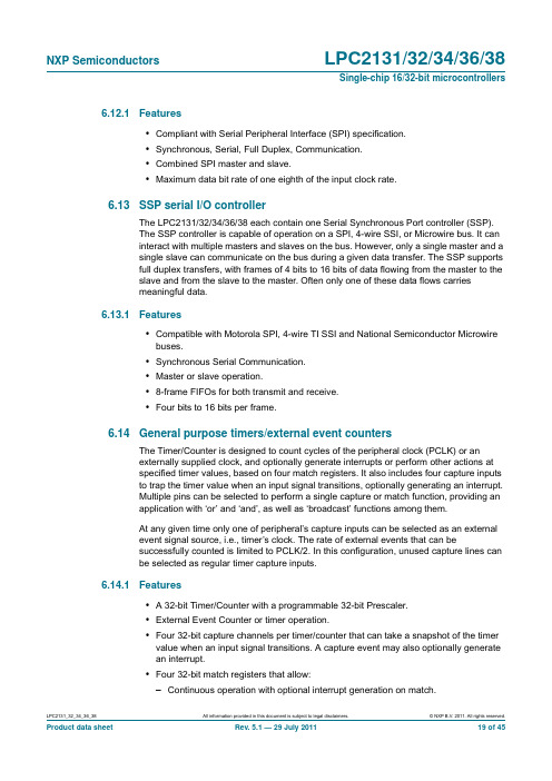
LPC2131_32_34_36_38All information provided in this document is subject to legal disclaimers.© NXP B.V. 2011. All rights reserved.Product data sheet Rev. 5.1 — 29 July 2011 19 of 45NXP Semiconductors LPC2131/32/34/36/38Single-chip 16/32-bit microcontrollers6.12.1Features•Compliant with Serial Peripheral Interface (SPI) specification.•Synchronous, Serial, Full Duplex, Communication.•Combined SPI master and slave.•Maximum data bit rate of one eighth of the input clock rate.6.13SSP serial I/O controllerThe LPC2131/32/34/36/38 each contain one Serial Synchronous Port controller (SSP).The SSP controller is capable of operation on a SPI, 4-wire SSI, or Microwire bus. It caninteract with multiple masters and slaves on the bus. However, only a single master and asingle slave can communicate on the bus during a given data transfer. The SSP supportsfull duplex transfers, with frames of 4 bits to 16 bits of data flowing from the master to theslave and from the slave to the master. Often only one of these data flows carriesmeaningful data.6.13.1Features•Compatible with Motorola SPI, 4-wire TI SSI and National Semiconductor Microwirebuses.•Synchronous Serial Communication.•Master or slave operation.•8-frame FIFOs for both transmit and receive.•Four bits to 16 bits per frame.6.14General purpose timers/external event countersThe Timer/Counter is designed to count cycles of the peripheral clock (PCLK) or anexternally supplied clock, and optionally generate interrupts or perform other actions atspecified timer values, based on four match registers. It also includes four capture inputsto trap the timer value when an input signal transitions, optionally generating an interrupt.Multiple pins can be selected to perform a single capture or match function, providing anapplication with ‘or’ and ‘and’, as well as ‘broadcast’ functions among them.At any given time only one of peripheral’s capture inputs can be selected as an externalevent signal source, i.e., timer’s clock. The rate of external events that can besuccessfully counted is limited to PCLK/2. In this configuration, unused capture lines canbe selected as regular timer capture inputs.6.14.1Features• A 32-bit Timer/Counter with a programmable 32-bit Prescaler.•External Event Counter or timer operation.•Four 32-bit capture channels per timer/counter that can take a snapshot of the timervalue when an input signal transitions. A capture event may also optionally generatean interrupt.•Four 32-bit match registers that allow:–Continuous operation with optional interrupt generation on match.LPC2131_32_34_36_38All information provided in this document is subject to legal disclaimers.© NXP B.V. 2011. All rights reserved.Product data sheet Rev. 5.1 — 29 July 2011 20 of 45NXP Semiconductors LPC2131/32/34/36/38Single-chip 16/32-bit microcontrollers–Stop timer on match with optional interrupt generation.–Reset timer on match with optional interrupt generation.•Four external outputs per timer/counter corresponding to match registers, with thefollowing capabilities:–Set LOW on match.–Set HIGH on match.–Toggle on match.–Do nothing on match.6.15Watchdog timerThe purpose of the watchdog is to reset the microcontroller within a reasonable amount oftime if it enters an erroneous state. When enabled, the watchdog will generate a systemreset if the user program fails to ‘feed’ (or reload) the watchdog within a predeterminedamount of time.6.15.1Features•Internally resets chip if not periodically reloaded.•Debug mode.•Enabled by software but requires a hardware reset or a watchdog reset/interrupt to bedisabled.•Incorrect/Incomplete feed sequence causes reset/interrupt if enabled.•Flag to indicate watchdog reset.•Programmable 32-bit timer with internal pre-scaler.•Selectable time period from (T cy(PCLK)⨯ 256⨯ 4) to (T cy(PCLK)⨯ 232⨯ 4) in multiples ofT cy(PCLK)⨯4.6.16Real-time clockThe Real-Time Clock (RTC) is designed to provide a set of counters to measure timewhen normal or idle operating mode is selected. The RTC has been designed to use littlepower, making it suitable for battery powered systems where the CPU is not runningcontinuously (Idle mode).6.16.1Features•Measures the passage of time to maintain a calendar and clock.•Ultra-low power design to support battery powered systems.•Provides Seconds, Minutes, Hours, Day of Month, Month, Year, Day of Week, andDay of Year.•Can use either the RTC dedicated 32 kHz oscillator input or clock derived from theexternal crystal/oscillator input at XTAL1. Programmable Reference Clock Dividerallows fine adjustment of the RTC.•Dedicated power supply pin can be connected to a battery or the main 3.3V.。

品牌机国产手机密码指令大全YUKI was compiled on the morning of December 16, 2020品牌机国产手机密码指令大全国产手机, 品牌机, 指令, 密码, 大全本帖最后由天空之上!于 2010-6-25 19:16 编辑一、各种品牌手机中英文对照acer::宏基 aiwa:爱华 alcatel(alc):阿尔卡特amoi:夏新 apbw:亚太 apple:苹果arcoa:全虹 asus:华硕 aux:奥克斯benq:明基 benten:巨腾 bird(brd):波导bosch:博士(博世) boss:宝石capitel:首信 casio:卡西欧 cect(cec):中电通讯chabridge:中桥 chase:采星 cosun:侨兴daewoo:大宇 datang:大唐 daxian:大显dbtel:迪比特 denso:电送 dnet:迪奈特doeasy:多易随 docomo :多科莫 dopod:多普达dragon:东方龙 eastcom(etcm):东信 emol:易美ericsson:爱立信 fuli:富利galaxy:银河 gionee:金立 giya:基雅gplus:积加 great:伟松 gsl:权智(快译通)gstar::吉事达 gvc:致福 hagenuk:汉佳诺haier(har):海尔 hisense:海信 hitachi:日立hutel:秀特尔 hyundai:现代 innostream:盈讯jpg:金鹏 jrc:日本无线kejian(kjn):科健 kenwood:建伍 kgt:和信konka(kon):康佳 kpt:先进电讯 kyocera(kyea):京瓷lenovo:联想 lucent:朗讯 lucky star:吉星malata:万利达 maxon:美晨 mitac:神达mitsubishi(trium):三菱 motorola:摩托罗拉nec:日本电气 nett:雷特 nintaus:金正nixxo:尼索 nokia(nki):诺基亚 nopo:星辰okwap:英资达 omron:欧姆龙palmax:帕玛斯(仁宝) panasonnic:松下 panda:熊猫penesas:天马 philips:飞利浦 photal:丰达putan:普天 qualcomm:高通 rowa:乐华sagem萨基姆 sanyo:三洋 samsung:三星sed:桑达 sendo:仙都 sewon:星王sharp:夏普 siemens:西门子 skynet:斯加耐特soutec:南方高科 sony:索尼 sobao:搜豹sonyerssion:索爱 soyea:数源 suohong:索鸿tcl:王牌 telsda:天时达 telson:泰尔信teltron:中讯天创 tinme:天梅(天美) tlink:神州龙tony:天珑(天龙) top:托普 toplux:天诺toshiba:东芝 toyo:东洋 transasia:泛亚ulycom:扬迪 uts:斯达康 victor:胜利vk:威科 vodafone:沃达丰 vtech:伟易达windows:视窗 xoceco:厦华ztc:中天伟业 zte:中兴品牌机系列二、手机密码(一)摩托罗拉摩托罗拉所有机锁:按menu+5+1/2t190解锁密码:t191解锁密码:3x8/2x88/998/8088/l2000/7689/t189/c289等初始密码为1234 ;话机密码为000000 ;解锁方法:如无测试卡,则先输入1234,如密码已更改,先按menu键会出现“修改开锁密码”,按ok键,然后输入000000就会显示四位数的话机密码,如保密码已更改,则只能用测试卡或软件工具解。

ME2-SFI 引擎控制模块
ABS,ASR,ETS,ESP 防抱死刹车,牵引力,车身稳定,动力转向控制模块ETC 变速箱控制模块
ESM 电子排挡控制模块
DTR 车距控制模块
AIR MATIC。
ABC 空气悬挂控制模块
TPS 胎压控制模块
SRS 气囊控制模块
EIS 电子点火开关控制模块
OCP 车顶控制模块
UCP 上控制台控制模块
SAM-FL 左前保险丝,继电器,车身控制模块
SAM-FR 右前保险丝,继电器车身控制模块
R-SAM 后保险丝,车身控制模块
AHE 拖车监控模块
KG 无钥匙进入控制模块
SVMCM 特殊车辆控制模块
PSE 中控真空泵控制模块
HRA 头灯调整控制模块
DCM-FL 左前门控制模块
DCM-FR 右前门控制模块
DCM-RL 右后门车身控制模块
DCM-RR 右后门控制模块
ESA-R 右前电动座椅
ESA 电动座椅
OSB-FL 左前座椅充气椅背控制模块
OSB-FR 右前座椅充气椅背控制模块
OSB-R 后座椅充气椅背控制模块
ICM 仪表控制模组
SCM 方向盘控制模组
D2B 光纤控制模组
CDC CD换片机控制模组
VCS 语言控制模组
CTEL1 行动电话控制模组1
CTEL2 行动电话控制模组2
SOUND 音响控制模组
PTS 倒车雷达控制模组
TELE AID 紧急求救控制模组
TV 电视调频控制模组
DN 卫星定位控制模组
AAC 冷气空调控制模组
REAR-AC 后冷气控制模组
STH 暖气加热控制模组。

Asian Pacific Journal of Cancer Prevention, Vol 14, 20132113DOI:/10.7314/APJCP .2013.14.3.2113MiR200a, miR93, RECK and MMP2/MMP9 Expression in Human Cervical CarcinomaAsian Pacific J Cancer Prev, 14 (3), 2113-2118IntroductionIn the worldwide, cervical cancer remains the third most common cancer in women globally after breast and colorectal cancer. However, 86% of all deaths caused by cervical cancer occur in developing countries (Arbyn et al., 2011). Data from the IARC GLOBOCAN 2008 database (http://globocan.iarc.fr/fact sheets/cancers/cervix.asp) estimate that there are 529, 512 new cases of cervical cancer diagnosed per year globally, corresponding to an age standardized incidence rate (ASIR) of 15.2/100,000 and 274,967 deaths. There is a striking difference in incidence of and mortality from cervical cancer in different regions of the world (Denny, 2012) So well-characteristic biomarkers are necessary for early diagnosis, to predict metastatic progression.Metastatic disease, rather than the primary tumor itself, is responsible for the death in most solid tumors, including cervical carcinoma (Lee et al., 1997; Welch et al., 2000; Yang et al., 2004). Degradation of basal membranes and the extracellular matrix (ECM) is essential for angiogenesis, invasion metastasis, and matrixDepartment of Obstetrics and Gynecology, the Second Affiliated Hospital of Jilin University, Changchun, Jilin, China *For correspondence: zanghu@AbstractAim and Background: Cervical cancer remains the third most common cancer in women globally after breast and colorectal cancer. Well-characterized biomarkers are necessary for early diagnosis and to predict metastatic progression and effective therapy. MiRNAs can regulate gene expression, cell growth, differentiation and apoptosis by targeting mRNAs for translational repression or degradation in tumor cells. The present study was conducted to assess expression of miR93, miR200a, RECK, MMP2, MMP9 in invasive cervical carcinoma, and analyze their clinical significance. Method: A total of 116 patients with invasive cervical carcinoma and 100 patients undergoing hysterectomy for benign lesions were retrospectively examined. Quantitative real-time PCR was performed to determine expression of miR93 and miR200a while RECK, MMP2, MMP9 and MVD were assessed by immunohistochemical staining. Results: Cervical carcinoma patients demonstrated up-regulation of miR-93, miR-200a, MMP2 and MMP9, with down-regulation of RECK as compared to benign lesion tissues. RECK was significantly inversely related to invasion and lymphatic metastasis. The 5-year survival rate for patients with strong RECK expression was significantly higher than that with weakly expressing tumors. Conclusion: MiR-93 and miR-200a are associated with metastasis and invasion of cervical carcinoma. Thus together with RECK they are potential prognostic markers for cervical carcinoma. RECK cooperating with MMP2, MMP9 expression is a significant prognostic factor correlated with long-term survival for patients with invasive cervical carcinoma.Keywords: miR-93 - miR-200a - RECK - MMP2 - MMP9 - MVD RESEARCH ARTICLEExpression of MiR200a, miR93, Metastasis-related Gene RECK and MMP2/MMP9 in Human Cervical Carcinoma - Relationship with PrognosisLing Wang, Qiang Wang, He-Lian Li, Li-Ying Han*metalloproteinases (MMPs) are potent enzymes that play a key role in these processes (Sabrina et al., 2012).Matrix Metalloproteinase 2 (MMP-2) (gelatinase A, 72 kDa) and Matrix Metalloproteinase 9 (MMP-9) (gelatinase B, 92 kDa) cleave type IV collagen and gelatin, which are the main structural components of the basal membrane (Toi et al., 1998). Expression of MMP-9 and MMP-2 has been implicated in the development and progression of many tumors, such as prostate, colorectal, breast cancer and cervical cancer (Liabakk et al., 1996; Kodate et al., 1997; Eissa et al., 2007; Rita et al., 2009).Several miRNAs are reported be associated with cervical carcinoma, Up-regulation of miR-200a and miR-93 promotes metastasis and tumor invasion. According to computational methodology current predictions-MicroCosm MMP2 is target gene to miR93, and TIMP1 is target gene to miR200a, while TIMP3 is target gene to miR93.MicroRNAs (miRNAs) is a novel class of small non-coding RNA molecules, 20-25 nucleotides in length, were shown to have important posttranscriptional gene regulatory functions. While miRNAs seed regionLing Wang et alAsian Pacific Journal of Cancer Prevention, Vol 14, 20132114which comprised of 2-8 nucleotides at 5’ end, target to special mRNA at 3’ untranslated region (UTR) (Bartel et al., 2009; Kim et al., 2009). If the complementarity of the miRNA-mRNA complex is perfect, miRNAs can exert translational repression function. However, if the complementarity is not perfect, the translation of the target mRNA is suppressed. To date, more than 1900 human mature miRNAs have been identified (http://www.miRbase. org/index. shtml), which are supposed to regulate more than 10% of protein coding genes (Wu et al., 2008), approximately one-third of expressed human genes contain miRNA regulatory target sites. Thus, this suggests that different clusters of miRNAs can regulate the cassette of specific genes which involve in one specific kind of cellular function together (Yang et al., 2003). It has been reported that RECK over-expression decreases the amount of active MMP-2 and MMP-9 and inhibits metastatic activity in vitro (Oh et al., 2001) and in vivo (Chang et al., 2008). RECK is a membrane-anchored glycoprotein of approximately 110 kDa containing multiple epidermal growth factor-like repeats and serine protease inhibitor-like domains. Down-regulation of RECK in several tumor cell lines and oncogene-transformed fibroblasts identified RECK as a common negative target for oncogenic signals. RECK low-expression, a hallmark of cancer, has been demonstrated to create a hypoxic tumor microenvironment.The aim of our study was to test the expression of miR200a and miR93 in cervical carcinoma, we propose the induction of the correlation between the expression of miR200a, miR93 and MMP2/9,RECK genes and to investigate whether miR200a, miR93 and MMP-2, MMP2/9 and RECK are expressed in a related pattern respectively in cervical carcinoma. Furthermore, we evaluate important prognostic parameters, analyzed the expression of RECK with 5-year survival rate, to conclude whether RECK is an independent factor to evaluate prognosis.Materials and MethodsTissue specimensCervical carcinoma specimens were obtained from patients undergone primary hysterectomy at the Department of Gynecology from Jan 2005 to Sep 2007, while control group were obtained from patients undergone hysterectomy for benign lesion. The specimens were frozen in liquid nitrogen at -80 ℃ within 30 minutes after isolated, and all cases were obtained from archives of the Department of Pathology in the Second Affiliated Hospital of Jilin University. The H&E stained slides of the cases were reviewed by gynecological pathologist. Morphology and protein expression were evaluated in consecutive sections. All protocols were reviewed and approved by the Ethical Committee of Second Affiliated Hospital of Jilin University. Written consent was obtained from all participating patients.Follow-upPatients were followed regularly for 5 years at the Second Affiliated Hospital of Jilin University. All patientswere followed until death or the study closing date (September 30, 2012). Disease-free survival (DFS) rate, which measured the first recurrence at any site, and overall survival (OS), measuring death from any case, were the two assessments used for prognostic analyses. Patients were re-examined (history, ultrasound examination, cervical screening test) once every 3 months during the first year, once every 6 months from the second year to the third year, and once every year after that. During the follow-up period, 6 patients were loss of follow up. 26 patients had disease recurrence and 36 patients died. miRNA isolationMiRNA was extracted from the tissue using the mirVana miRNA Isolation Kit (AM1561, Ambion) for hysterectomy specimen according to the protocols. The quantity and quality of the miRNA was verified with the NanoDrop spectrophotometer (Thermo Fisher Scientific Incorporated, Wilmington DE, USA) according to the manufacturer’s instructions.Quantitative real-time PCR (QPCR)miRNAs was reverse transcribed in a 20 μl reaction using the one step primescript miRNA cDNA Synthesis Kit (Takara, D350A). Forward primer sequences miR93: CAAAGTGCTGTTCGTGCAGGTAG, miR200a: GTAA CACTGTCTGGTAACGATGQPCR was performed on a BioMad Real-Time PCR System (ABI) using Power- SYBR Green PCR Master Mix (Takara, DRR081) in a 20 μl reaction and U6 as an endogenous control, miRlet-7 as positive control, result was determined using the 2-ΔΔCT . The QPCR experiments were run triplely within each experiment run, relative expression values were normalized to standard deviations from the mean.Immunohistochemical stainTo determine the expression of RECK, MMP2, MMP9 and MVD, immunohistochemical staining was carried out using the two-step plus poly-HRP method as described previously. After blocking with 3% hydrogen peroxide, the slides were incubated with primary anti-RECK antibody, anti-MMP2 antibody, anti-MMP9 antibody and CD34 antibody (1:50 goat mAb respectively; Santa Cruz Biotechnology, Santa Cruz, CA, USA). Afterwards, the slides were stained with the two-step plus poly-HRP antigoat IgG detection system (ZSGB-Bio, Beijing, China). For negative controls, the primary antibody was substituted with PBS in order to confirm the specificity of the primary antibody.Evaluation of immunohistochemical stainingTwo experienced investigators, who provided a consensus opinion of stain patterns by light microscopy, evaluated sections. RECK, MMP2 and MMP9 expression was estimated from the staining intensity and graded as follows: Grade 0, no staining (-); Grade 1, faint staining (+); Grade 2, moderate staining (++); and Grade 3, strong staining (+++). The positively stained area (distribution) was expressed as the percentage of the whole area under evaluation and scored as follows: 0, no staining; 1, 1~25% positive cells; 2, 26~50% positive cells; 3, 51~75%Asian Pacific Journal of Cancer Prevention, Vol 14, 20132115P0.0002 0.0193 0.0062Table 2. Correlation Between RECK Expression andVarious Clinicopathological Features in Cervical Cancer PatientsN RECK positive χ2 Pnegative positive (%)Stage I 64 33 31 48.44 6.198 0.1024 II 33 21 12 36.36 III 17 12 5 29.41 IV 2 2 0 0 Grade I 23 13 10 43.48 3.6204 0.1636 II 63 42 21 33.33 III 30 15 15 50 Invasive depth T2 66 43 23 34.85 0.0184 T3-T4 50 36 24 48 Lymph node status N1-N3 15 14 1 6.67 0.0237 N0 101 58 53 52.48 Squamous carcinoma 99 60 39 39.4 1 adenocarcinoma 17 11 6 35.29in Cervical Carcinoma in Relation to Normal TissueA BFigure 2. Expression of RECK, MMP2, MMP9. (A)expression of RECK in control group; (B) expression of RECK in cervical carcinoma; (C) expression of MMP2 in cervical carcinoma; (D) expression of MMP9 in cervical carcinoma; (E) MVD expression in control group; (F) expression of MVD in cervical carcinomapositive cells; and 4, 76~100% positive cells. Overall expression was then graded as low expression (score 0~2), intermediate expression (score 3~5), and high expression (score 6~7).Statistical analysisAnalysis were carried out by BioMad CFX system and statistical software SPSS 14.0 (SPSS, Chicago, IL, USA). The correlation of RECK, MMP2/9 expression with patients’ clinicopathological factors was analyzed by the Fisher’s exact test. The Kaplan-Meier method was used to estimate OS. Survival differences according to RECK expression were analyzed by the log-rank test. The risk ratio and its 95% confidence interval were recorded for each marker. P -values< 0.05 were considered statistically significant in all of the analysis.ResultsMean age of the total 116 patients was 49.3±2.39 years (24~77 years). 36 patients (31.03%) died, and 74 patients (63.79%) were alive at the end of research. Results of qPCR showed that miR93 and miR200a expression was higher in cervical carcinoma tissues (Figure 1A, Figure 1B). RECK was detected in the cytoplasm of normal cells (Figure 2A, Figure 2B), and of cervical carcinoma specimen its expression was much lower than that in control group, MMP9, MMP2 was detected in the cytoplasm of cells (Figure 2C, Figure 2D). MMP2 and MMP9 expression was significantly higher in cervical carcinoma than that in control group (Table 1). Accordingto Cox regression analysis result, the expression of MMP2 was positively related to expression of miR93 (P =0.0027) and miR200a (P =0.0016). However, higher expression of RECK related to lower expression of MMP2, MMP9. We also examined positive RECK staining in different clinopathological factors such as stage, grade, invasion depth and lymph node metastasis (Table 2). These data indicated that the frequency of RECK expression in high-grade was much higher than in low-grade cervical carcinoma. RECK expression, however, was significantly associated with lymph node metastasis (P =0.0237)Ling Wang et alAsian Pacific Journal of Cancer Prevention, Vol 14, 20132116and invasive depth (P =0.0184). Lymph node negative patients had higher RECK expression (53/101, 52.48%) than lymph node positive patients (1/15, 6.67%). Deeper invasive patients had lower RECK expression (24/50, 48%) than lower invasive patients (23/66, 34.85%). We found that histopathological grade, pathological TNM stage have no significance as prognostic predicators (Table 2). Multivariate analysis was carried out on the same set of patients for RECK expression and pathological predictors using the Cox regression model. The results indicated that RECK status (risk ratio, 3.312; P <0.05) was independent prognostic factor.Microscopic observation of MVD staining showed that in cervical carcinoma group, micro-vascular arranged disorderly, size and shape were irregular, thickness of vascular wall was nonuniform (Figure 2F), while in control group, clearer expression of micro-vascular endothelial cells were round or oval and in regular shape (Figure 2E). According to the Cox regression analysis, RECK expression in cervical carcinoma was negatively associated with MVD value (r=-0397, p =0.0495) (Table 3).To determine the relation between RECK expression and prognosis, Patients were divided into two groups on the basis of their prognosis. Our results indicated that patients with a poor prognosis(recurrence or metastasis) had low levels of RECK expression (P <0.05). Kaplan-Meier survival analysis showed that RECK positive patients also had significantly higher OS rates (P <0.05, log-rank test; Figure 3A).RECK positive patients had higher DFS rates compared with RECK negative patients (P =0.0387, log-rank test; Figure 3B).DiscussionAccumulating reports demonstrated that miRNAs have been observed in a variety of human cancers, and miRNA signatures accurately reflect the developmental lineagesand differential expression states of tumors by microarray profiling studies (Lu et al., 2005; Rosenfeld et al., 2008) Furthermore, they certified miRNAs involved in tumor cells invasion, apoptosis, angiogenesis and metastasis through regulation to target genes of corresponding signal pathways (MA et al., 2012). In previous research on human cervical cancer, expression of miR-15a, miR-20b, miR-21 and miR-224 is obviously increased in tissue and let-7c, miR-143, miR-199a-5p, miR-203 and miR-145 is reduced (Pereira et al., 2010; Wang et al., 2008). In our study, miRNAs expressions were quantified by using quantitative real-time PCR in which miR-93, miR-200a were up-regulated in cervical carcinoma tissue. Their expressions were accompanied by over-expression in MMP-2, MMP-9 and suppression in RECK gene.The miR-93 gene is located on chromosome 7q22.1, it can suppress proliferation and differentiation of cancer stem cells, while promoting tumor growth and malignant cells survival (Fang et al., 2011; Yu et al., 2011; Suling et al., 2012). In the present study, mir-93 expression was 5.29 fold higher compared to normal tissue. Our data are consistent with other reports indicating that mir-93 expression increased with cervical carcinoma (Lui et al., 2007). By microcosm predictor system, MMP2 has the target gene in 3’ UTR to miR-93, also TIMP3 is the proposal target gene of miR-93 ,whose sequence GAUGGACGUGCUUGUCGUGAAA was relatively complemented with CTTTCTATGTGCAAGGCACTTT in TIMP3 (/enright-srv /microcosm/htdocs/targets/v5). Endogenous angiogenesis inhibitors TIMPs are necessary to block the mitogenic stimuli in the vascular endothelium (Curran et al., 2000). TIMP3 is inhibitor of MMP2 and associated with actin and serve to stabilize microfilaments, so it act as tumor suppressor gene (Perry, 2001). miR93 was indentified up-regulated expression of MMP2 in cervical carcinoma, for the up-regulated mir-93, the inhibiting function of tumor suppressor genes TIMP3 maybe suppressed. But this hypothesis has not been certified. The miR-200a gene is located on chromosome 1P36.33, and can enhance invasion and growth of malignant cells. In this study, miR-200a was over-expressed by 3.65 folds in cervical carcinoma compared to normal tissues respectively. Similar studies indicated the miR-200a was up regulated which may supporting the concept that miR-200a functions as oncogene (Cong et al., 2013; Rasheed et al., 2013; Yu et al., 2013). In our study, the over-expression of miR-200a was associated with the over-expression of MMP2, MMP9. According to Microcosm target gene predictor system, TIMP1 is the corresponding target gene of miR-200a. miR-200a has been supposed to involve in down-regulating of TIMP1, whose inhibitor function to MMP2 and MMP9 is weakened and led to over-expression of MMP2 and MMP9. Similar research instructed that miR-200b is overexpressed in endometrial adenocarcinomas and enhances MMP2 activity by down regulating TIMP2 in human endometrial cancer cell Line HEC-1A cells (Dai et al., 2013). But the accurate mechanism in cervical carcinoma still need to certified in vitro until now.In this research, RECK expression is suppressedTable 3. Expression of MVD in Cervical Carcinoma and Control Tissue (n)P n MVD P RECK r (n/*400) (positive) [n(%)] Cervical carcinoma 116 19.4615±3.0718 0.000 48(40.31) -0.397Control group 100 12.0000±2.6629 0.0495 86(86.0)Figure 3. Kaplan–eier Analysis for Disease-free Survival (DFS) and Overall Survival (OS) Based on RECK Expression in Cervical Carcinoma Patients.(A) Kaplan–Meier analysis for OS based on RECK expression in patients with cervical carcinoma (P =0.0399, log–rank test); (B) Kaplan–Meier analysis for DFS based on RECK expression in patients with cervical carcinoma (P = 0.0387, log–rank test). RECK(+): RECK-positive patients (n =48 ); RECK(-): RECK-negative patients (n = 68)Asian Pacific Journal of Cancer Prevention, Vol 14, 20132117DOI:/10.7314/APJCP .2013.14.3.2113MiR200a, miR93, RECK and MMP2/MMP9 Expression in Human Cervical Carcinomain cervical carcinoma tissue when compared to benign lesion tissue. There are almost certainly pathways by which RECK is down-regulated in cancer. Hypoxia induces RECK down-regulation through the recruitment of HDAC1 and HIF-1α to the rHRE2 site in the promoter and the inhibition of hypoxic RECK silencing would be a therapeutic and preventive target for early tumorigenesis (Zhang et al., 2012). However, the CpG island promoter hypermethylation is associated silencing of tumor suppressor genes, which is the most recognized epigenetic disruption in human tumors (Rodriguez et al., 2011). Low RECK expression is closely correlated with high MMP2, MMP9 expression. In addition, increased expression of MMP2, MMP9 with decreased expression of RECK in invasive cervical carcinoma irrespective of histological grading supports the fact that RECK has a negative effect on the invasiveness of cervical cancer. Mori had found (Mori T et al., 2007) that MMP-2 activity, but not its mRNA expression, was significantly down-regulated in HT1080 cells after they were transferred into the RECK plasmid (Bin Zhang et al., 2009). Similarly, our results showed a negative correlation between RECK and MMP-2 protein expression. In HUVECs, specific inhibition of MMP-2 significantly antagonized the effect of RECK depletion on β1-integrin signaling, cell proliferation, and tube elongation (Namwat et al., 2011). Moreover, RECK-mediated suppression of MMP-9 promoter activity requires 12-O- tetradecanoylphorbol-13-acetate-responsive element (TRE) and KB sites. Moreover, the binding ability of Fra-1 and c-Jun to TRE within the MMP-9 promoter region was suppressed by RECK (Satoshi et al., 2007). In this research, MVD CD34 for tumors with lower-expression RECK is obviously increased, which indicates that RECK can inhibit angiogenesis. Targeting RECK specifically in tumor-associated vascular endothelial cells resulted in tumor regression (Takao et al., 2010).RECK positive patients showed higher 5-year survival rates and DFS rates. Furthermore, we found that RECK expression was significantly associated with lymph node metastasis and deeper invasion. HER-2/neu oncogene inhibits the expression of RECK to promote cell invasion (Tsung-Te et al., 2012). Hypermethylation of RECK promoter is also a common event in human ESCC, which occurs concurrently in tumor-adjacent normal mucosa and is correlated with poor prognosis in ESCC patients (Long NK et al., 2008). RECK displays as a metastasis suppressor and up-regulation of RECK expression could provide a potential therapy to improve the prognosis (Namwat et al., 2011).In conclusion, MiR-93, miR-200a is associated with metastasis and invasion of cervical carcinoma, thus MiR-93, miR-200a, RECK expression is a potentially prognostic marker for cervical carcinoma. RECK cooperating with MMP2, MMP9 expression is a significant prognostic factor correlated with long-term survival for patients with invasive cervical carcinoma.ReferencesArbyn M, Andersson K, Bergeron C, et al (2011). Cervicalcytology biobanks as a resource for molecular epidemiology. Methods Mol Biol , 675, 279-98.Bartel DP (2009). MicroRNAs, target recognition and regulatoryfunctions. Cell , 136, 215-33.Chang CK, Hung WC, Chang HC (2008). The Kazal motifs ofRECK protein inhibit MMP-9 secretion and activity and reduce metastasis of lung cancer cells in vitro and in vivo. J Cell Mol Med , 12, 12-6.Cong N, Du P , Zhang A, et al (2013). Downregulated microRNA-200a promotes EMT and tumor growth through the wnt/β-catenin pathway by targeting the E-cadherin repressors ZEB1/ZEB2 in gastric adenocarcinoma. Oncol Rep , 10, 3892-7.Curran S, Murray GI (2000). Matrix metalloproteinases,molecular aspects of their roles in tumour invasion and metastasis. Eur J Cancer , 36, 1621-30Dai Y, Xia W, Song T, et al (2013). MicroRNA-200b isoverexpressed in endometrial adenocarcinomas and enhances MMP2 activity by downregulating TIMP2 in human endometrial cancer cell line HEC-1A cells. Nucleic Acid Ther , 23, 29-34.Denny Lynette (2012). Cervical cancer, prevention andtreatment. Discov Med , 14, 125-11.Eissa S, Ali-Labib R, Swellam M, et al (2007). Noninvasivediagnosis of bladder cancer by detection of matrix metalloproteinases (MMP-2 and MMP-9) and their inhibitor (TIMP-2) in urine. Eur Urol , 52, 1388-96.Fang L, Deng Z, Shatseva T, et al (2011). MicroRNA miR-93promotes tumor growth and angiogenesis by targeting integrin-β8. Oncogene , 30, 806-21.Figueira RC, Gomes LR, Neto JS, et al (2009). Correlationbetween MMPs and their inhibitors in breast cancer tumor tissue specimens and in cell lines with different metastatic potential. BMC Cancer , 9, 20-5.Liu S, Patel SH, Ginestier C, et al (2012). MicroRNA93 regulatesproliferation and differentiation of normal and malignant breast stem cells. PLoS Genet , 8, e1002751.Kim VN, Han J, Siomi MC (2009). Biogenesis of small RNAsin animals. Nat Rev Mol Cell Biol , 10, 126-39.Kodate M, Kasai T, Hashimoto H, et al (1997). Expression ofmatrix metalloproteinase (gelatinase) in T1 adenocarcinoma of the lung. Pathol Int , 47, 461-9.Lee JH, Welch DR (1997). Suppression of metastasis in humanbreast carcinoma MDA-MB-435 cells after transfection with the metastasis suppressor gene, KiSS-1. Cancer Res , 57, 2384-7.Liabakk NB, Talbot I, Smith RA, et al (1996). Matrix metallo-proteinase 2 (MMP-2) and matrix metalloproteinase 9 (MMP-9) type IV collagenase in colorectal cancer. Cancer Res , 56, 190-6.Lim LP, Lau NC, Garrett-Engele P, et al (2005). Microarrayanalysis shows that some microRNAs downregulate large numbers of target mRNAs. Nature , 433, 769-73.Long NK, Kato K, Yamashita T, et al (2008). Hypermethylationof the RECK gene predicts poor prognosis in oral squamous cell carcinomas. Oral Oncol , 44, 1052-8.Lu J, Getz G, Miska EA, et al (2005). MicroRNA expressionprofiles classify human cancers. Nature , 435, 834-8.Lui WO, Pourmand N, Patterson BK, Fire A (2007). Patternsof known and novel small RNAs in human cervical cancer. Cancer Res, 67, 6031-43.Ma D, Zhang YY , Guo YL, Li ZJ, Geng L (2012). Profiling ofmicroRNA-mRNA reveals roles of microRNAs in cervical cancer. Chin Med J , 125, 4270-76.Mori T, Moriuchi R, Okazaki E, et al (2007). Tgat oncoproteinfunctions as a inhibitor of RECK by association of the unique C-terminal region. Biochem Biophys Res Commun ,Ling Wang et alAsian Pacific Journal of Cancer Prevention, Vol 14, 20132118355, 937-43.Namwat N, Puetkasichonpasutha J, Loilome W, et al (2011).Downregulation of reversion-inducing-cysteine-rich protein with Kazal motifs (RECK) is associated with enhanced expression of matrix metalloproteinases and cholangiocarcinoma metastases. J Gastroenterol, 46, 664-75.Oh J, Takahashi R, Kondo S, et al (2001). The membraneanchored MMP inhibitor RECK is a key regulator of extracellular matrix integrity and angiogenesis. Cell , 107, 789-800.Pereira PM, Marques JP, Soares AR, Carreto L, Santos MA(2010). MicroRNA expression variability in human cervical tissues. PLoS One , 5, e11780.Perry SV (2001). V ertebrate tropomyosin, distribution, propertiesand function. J Muscle Res Cell Motil , 22, 5-49.Rasheed SA, Teo CR, Beillard EJ, V oorhoeve M, Casey PJ(2013). MicroRNA-182 and microRNA-200a control G-protein subunit alpha-13 (GNA13) expression and cell invasion synergistically in prostate cancer. Cells J Biol Chem , 10, 1074-7.Rodriguez-Paredes M, Esteller M (2011). Cancer epigeneticsreaches mainstream oncology. Nat Med , 17, 330-9.Rosenfeld N, Aharonov R, Meiri E, Rosenwald S, et al (2008).MicroRNAs accurately identify cancer tissue origin. Nat Biotechnol, 26, 462-9.Reis ST, Leite KR, Piovesan LF, et al (2012). Increasedexpression of MMP-9 and IL-8 are correlated with poor prognosis of Bladder Cancer. BMC Urol , 12, 18-23.Takagi S, Simizu S, Osada H (2009). RECK negatively regulatesmatrix metalloproteinase-9 transcription. Cancer Res , 69, 1502-8.Miki T, Shamma A, Kitajima S, et al (2010). TThe ß1-integrin-dependent function of RECK in physiologic and tumor angiogenesis. Mol Cancer Res , 8, 665-76.TChung TT, Yeh CB, Li YC, et al (2012). Effect of RECK genepolymorphisms on hepatocellular carcinoma susceptibility and clinicopathologic features. Plos one , 7, e33517.Toi M, Ishigaki S, Tominaga T(1998). Metalloproteinases andtissue inhibitors of metallo-proteinases. Breast Cancer Res Treat , 52, 113-24.Wang X, Tang S, Le SY , et al(2008). Aberrant expression ofoncogenic and tumor-suppressive microRNAs in cervical cancer is required for cancer cell growth. PLoS One, 3, e2557.Welch DR, Steeg PS, Rinker-Schaeffer CW (2000). Molecularbiology of breast cancer metastasis. Genetic regulation of human breast carcinoma metastasis. Breast Cancer Res , 2, 408-16.Wu L, Belasco JG (2008). Let me count the ways, mechanisms ofgene regulation by miRNAs and siRNAs. Mol Cell, 29, 1-7.Yang J, Mani SA, Donaher JL, et al (2004). Twist, a masterregulator of morphogenesis, plays an essential role in tumor metastasis. Cell , 117, 927-39.Yang L, Parkin DM, Li L, Chen Y (2003). Time trends in cancermortality in China, 1987-1999. Int J Cancer , 106, 771-83.Yu SJ, Hu JY, Kuang XY, et al (2013). MicroRNA-200aPromotes Anoikis Resistance and Metastasis by Targeting YAP1 in Human Breast Cancer. Clin Cancer Res , 10, 1158-63.Yu XF, Zou J, Bao ZJ, Dong J (2011). miR-93 suppressesproliferation and colony formation of human colon cancer stem cells. World J Gastroenterol , 17, 4711-7.Zhang B, Zhang J, Xu ZY , Xie HL (2009). Expression of RECKand matrix metalloproteinase-2 in ameloblastoma. BMC Cancer , 9, 427-35.Zhang C, Ling Y , Zhang C, et al (2012). The silencing of RECKgene is associated with promoter hypermethylation and poorsurvival in hepatocellular carcinoma. Int J Biol Sci , 8, 451-8.。

Micron Serial NOR Flash Memory 1.8V, Multiple I/O, 4KB Sector EraseN25Q032AFeatures•SPI-compatible serial bus interface•108 MHz (MAX) clock frequency•1.7–2.0V single supply voltage•Dual/quad I/O instruction provides increased throughput up to 432 MHz•Supported protocols–Extended SPI, dual I/O, and quad I/O •Execute-in-place (XIP) mode for all three protocols –Configurable via volatile or nonvolatile registers –Enables memory to work in XIP mode directly af-ter power-on•PROGRAM/ERASE SUSPEND operations •Continuous read of entire memory via a single com-mand–Fast read–Quad or dual output fast read–Quad or dual I/O fast read•Flexible to fit application–Configurable number of dummy cycles–Output buffer configurable•Software reset•64-byte, user-lockable, one-time programmable (OTP) dedicated area•Erase capability–Subsector erase 4KB uniform granularity blocks –Sector erase 64KB uniform granularity blocks–Full-chip erase •Write protection–Software write protection applicable to every 64KB sector via volatile lock bit–Hardware write protection: protected area size defined by four nonvolatile bits (BP0, BP1, BP2,and TB)–Additional smart protections, available upon re-quest•Electronic signature–JEDEC-standard 2-byte signature (BB16h)–Unique ID code (UID): 17 read-only bytes, in-cluding:•Two additional extended device ID (EDID)bytes to identify device factory options•Customized factory data (14 bytes)•Minimum 100,000 ERASE cycles per sector •More than 20 years data retention•Packages JEDEC standard, all RoHS compliant–F4 = UF-PDFN-8 4mm x 3mm (MLP8 4mm x 3mm)–F6 = V-PDFN-8 6mm x 5mm ( MLP8 6mm x 5mm )–F8 = V-PDFN-8 8mm x 6mm (MLP8 8mm x 6mm)–12 = T-PBGA-24b05 6mm x 8mm–SF = SOP2-16 300 mils body width (SO16W)–SE = SOP2-8 208 mils body width (SO8W)质量等级领域:宇航级IC、特军级IC、超军级IC、普军级IC、禁运IC、工业级IC,军级二三极管,功率管等;应用领域:航空航天、船舶、汽车电子、军用计算机、铁路、医疗电子、通信网络、电力工业以及大型工业设备祝您:工作顺利,生活愉快!以深圳市美光存储技术有限公司提供的参数为例,以下为N25Q032A11EF640F的详细参数,仅供参考Device DescriptionThe N25Q is the first high-performance multiple input/output serial Flash memory de-vice manufactured on 65nm NOR technology. It features execute-in-place (XIP) func-tionality, advanced write protection mechanisms, and a high-speed SPI-compatible businterface. The innovative, high-performance, dual and quad input/output instructionsenable double or quadruple the transfer bandwidth for READ and PROGRAM opera-tions.FeaturesThe memory is organized as 64 (64KB) main sectors that are further divided into 16 sub-sectors each (1024 subsectors in total). The memory can be erased one 4KB subsector ata time, 64KB sectors at a time, or as a whole.The memory can be write protected by software through volatile and nonvolatile pro-tection features, depending on the application needs. The protection granularity is of64KB (sector granularity) for volatile protectionsThe device has 64 one-time programmable (OTP) bytes that can be read and program-med with the READ OTP and PROGRAM OTP commands. These 64 bytes can also bepermanently locked with a PROGRAM OTP command.The device also has the ability to pause and resume PROGRAM and ERASE cycles by us-ing dedicated PROGRAM/ERASE SUSPEND and RESUME instructions.Operating ProtocolsThe memory can be operated with three different protocols:•Extended SPI (standard SPI protocol upgraded with dual and quad operations)•Dual I/O SPI•Quad I/O SPIThe standard SPI protocol is extended and enhanced by dual and quad operations. Inaddition, the dual SPI and quad SPI protocols improve the data access time andthroughput of a single I/O device by transmitting commands, addresses, and dataacross two or four data lines.XIP ModeXIP mode requires only an address (no instruction) to output data, improving randomaccess time and eliminating the need to shadow code onto RAM for fast execution.All protocols support XIP operation. For flexibility, multiple XIP entry and exit methodsare available. For applications that must enter XIP mode immediately after poweringup, XIP mode can be set as the default mode through the nonvolatile configuration reg-ister bits.Signal DescriptionsThe signal description table below is a comprehensive list of signals for the N25 familydevices. All signals listed may not be supported on this device. See Signal Assignmentsfor information specific to this device.32Mb, 1.8V, Multiple I/O Serial Flash MemoryNonvolatile and Volatile Registers Nonvolatile and Volatile RegistersThe device features the following volatile and nonvolatile registers that users can accessto store device parameters and operating configurations:•Status register•Nonvolatile and volatile configuration registers•Enhanced volatile configuration register•Flag status register•Lock registerNote: The lock register is defined in READ LOCK REGISTER Command.In addition to these user-accessible registers, the working condition of memory is set byan internal configuration register that is not directly accessible to users. As shown be-low, parameters in the internal configuration register are loaded from the nonvolatileconfiguration register during each device boot phase or power-on reset. In this sense,then, the nonvolatile configuration register contains the default settings of memory.Also, during the life of an application, each time a WRITE VOLATILE or ENHANCEDVOLATILE CONFIGURATION REGISTER command executes to set configuration pa-rameters in these respective registers, these new settings are copied to the internal con-figuration register. Therefore, memory settings can be changed in real time. However, atthe next power-on reset, the memory boots according to the memory settings definedin the nonvolatile configuration register parameters.。

ArchitectureThese devices use NAND Flash electrical and command interfaces. Data, commands,and addresses are multiplexed onto the same pins and received by I/O control circuits.The commands received at the I/O control circuits are latched by a command register and are transferred to control logic circuits for generating internal signals to control de-vice operations. The addresses are latched by an address register and sent to a row de-coder to select a row address, or to a column decoder to select a column address.Data is transferred to or from the NAND Flash memory array, byte by byte, through a data register and a cache register.The NAND Flash memory array is programmed and read using page-based operations and is erased using block-based operations. During normal page operations, the data and cache registers act as a single register. During cache operations, the data and cache registers operate independently to increase data throughput.The status register reports the status of die (LUN) operations.Figure 7: NAND Flash Die (LUN) Functional Block DiagramCE#CLEN/A ALERE#WP#DQ[7:0]Async WE#R/B#CE#CLE DQSALE W/R#WP#DQ[7:0]SyncCLK R/B#Notes: 1.N/A: This signal is tri-stated when the asynchronous interface is active.2.Some devices do not include the synchronous interface.16Gb, 32Gb, 64Gb Asynchronous/Synchronous NAND Architecturedriver enables multiple R/B# outputs to be OR-tied. Typically, R/B# is connected to an interrupt pin on the system controller (see Figure 18 (page 28)).The combination of Rp and capacitive loading of the R/B# circuit determines the rise time of the R/B# signal. The actual value used for Rp depends on the system timing re-quirements. Large values of Rp cause R/B# to be delayed significantly. Between the 10-to 90-percent points on the R/B# waveform, the rise time is approximately two time constants (TC).TC = R × CWhere R = Rp (resistance of pull-up resistor), and C = total capacitive load.The fall time of the R/B# signal is determined mainly by the output impedance of the R/B# signal and the total load capacitance. Approximate Rp values using a circuit load of 100pF are provided in Figure 23 (page 31).The minimum value for Rp is determined by the output drive capability of the R/B# sig-nal, the output voltage swing, and Vccq.Rp =Vcc (MAX) - Vol (MAX)IOL + ΣilWhere Σil is the sum of the input currents of all devices tied to the R/B# pin. Figure 18: READ/BUSY# Open Drain16Gb, 32Gb, 64Gb Asynchronous/Synchronous NAND Bus Operation – Asynchronous InterfaceREAD PAGE CACHE SEQUENTIAL (31h)The READ PAGE CACHE SEQUENTIAL (31h) command reads the next sequential page within a block into the data register while the previous page is output from the cache register. This command is accepted by the die (LUN) when it is ready(RDY = 1, ARDY = 1). It is also accepted by the die (LUN) during READ PAGE CACHE (31h, 00h-31h) operations (RDY = 1 and ARDY = 0).To issue this command, write 31h to the command register. After this command is is-sued, R/B# goes LOW and the die (LUN) is busy (RDY = 0, ARDY = 0) for t RCBSY. After t RCBSY, R/B# goes HIGH and the die (LUN) is busy with a cache operation(RDY = 1, ARDY = 0), indicating that the cache register is available and that the specified page is copying from the NAND Flash array to the data register. At this point, data can be output from the cache register beginning at column address 0. The CHANGE READ COLUMN (05h-E0h) command can be used to change the column address of the data being output from the cache register.The READ PAGE CACHE SEQUENTIAL (31h) command can be used to cross block boundaries. If the READ PAGE CACHE SEQUENTIAL (31h) command is issued after the last page of a block is read into the data register, the next page read will be the next logi-cal block in the plane which the 31h command was issued. Do not issue the READ PAGE CACHE SEQUENTIAL (31h) to cross die (LUN) boundaries. Instead, issue the READ PAGE CACHE LAST (3Fh) command.If the READ PAGE CACHE SEQUENTIAL (31h) command is issued after a MULTI-PLANE READ PAGE operation (00h-32h, 00h-30h), the next sequential pages are read into the data registers while the previous pages can be output from the cache registers.After the die (LUN) is ready (RDY = 1, ARDY = 0), the CHANGE READ COLUMN EN-HANCED (06h-E0h) command is used to select which cache register outputs data.Figure 47: READ PAGE CACHE SEQUENTIAL (31h) OperationPage M Page M+116Gb, 32Gb, 64Gb Asynchronous/Synchronous NAND Read Operations。


Notes: 1.Maximum limit not applicable.2.Micron tDLLK values support the legacy JEDEC tDLLK specifications.3.DDR4-1600 AC timing parameters apply if DRAM operates at lower than 1600 MT/s data rate.4.Data rate is greater than or equal to 1066 Mb/s.5.WRITE-to-READ when CRC and DM are both not enabled.6.WRITE-to-READ delay when CRC and DM are both enabled.7.The start of internal write transactions is defined as follows:•For BL8 (fixed by MRS and on-the-fly): rising clock edge four clock cycles after WL •For BC4 (on-the-fly): rising clock edge four clock cycles after WL•For BC4 (fixed by MRS): rising clock edge two clock cycles after WL8.For these parameters, the device supports t n PARAM [n CK] = ROUND{t PARAM [ns]/t CK (AVG) [ns]} according to the rounding algorithms found in the Converting Time-Based Specifications to Clock-Based Requirements section, in clock cycles, assuming all input clock jitter specifications are satisfied.9.When operating in 1t CK WRITE preamble mode.10.When operating in 2t CK WRITE preamble mode.11.When CA parity mode is selected and the DLLoff mode is used, each REF command re-quires an additional "PL" added to t RFC refresh time.12.DRAM devices should be evenly addressed when being accessed. Disproportionate ac-cesses to a particular row address may result in reduction of the product lifetime and/or reduction in data retention ability.13.Applicable from t CK (AVG) MIN to t CK (AVG) MAX as stated in the Speed Bin tables.14.JEDEC specifies a minimum of five clocks.15.The maximum read postamble is bound by t DQSCK (MIN) plus t QSH (MIN) on the left side and t HZ(DQS) MAX on the right side.16.The reference level of DQ output signal is specified with a midpoint as a widest part of output signal eye, which should be approximately 0.7 × V DDQ as a center level of the static single-ended output peak-to-peak swing with a driver impedance of 34 ohms and an effective test load of 50 ohms to V TT = V DDQ .17.JEDEC hasn't agreed upon the definition of the deterministic jitter; the user should fo-cus on meeting the total limit.18.Spread spectrum is not included in the jitter specification values. However, the input clock can accommodate spread-spectrum at a sweep rate in the range of 20–60 kHz with an additional 1% of t CK (AVG) as a long-term jitter component; however, the spread spectrum may not use a clock rate below t CK (AVG) MIN.19.The actual t CAL minimum is the larger of 3 clocks or 3.748ns/t CK; the table lists the ap-plicable clocks required at targeted speed bin.20.The maximum READ preamble is bounded by t LZ(DQS) MIN on the left side and t DQSCK (MAX) on the right side. See figure in the Clock to Data Strobe Relationship section.Boundary of DQS Low-Z occurs one cycle earlier in 2t CK toggle mode, as illustrated in the READ Preamble section.21.DQ falling signal middle-point of transferring from HIGH to LOW to first rising edge of DQS differential signal cross-point.22.The t PDA_S/t PDA_H parameters may use the t DS/t DH limits, respectively, if the signal is LOW the entire BL8.8Gb: x4, x8, x16 DDR4 SDRAM AC Electrical Characteristics and AC Timing ParametersFigure 242: tADC Definition with Direct ODT ControlDODTLoff DODTLon Figure 243: tADC Definition with Dynamic ODT ControlODTLcnw ODTLcnw4/88Gb: x4, x8, x16 DDR4 SDRAM Electrical Characteristics – On-Die Termination CharacteristicsFigure 13: 96-Ball FBGA – x16 (TB)Ball A1 ID (covered by SR)1.8 CTRNonconductiveovermold Notes: 1.All dimensions are in millimeters.2.Solder ball material: SAC302 (96.8% Sn, 3% Ag, 0.2% Cu).8Gb: x4, x8, x16 DDR4 SDRAM Package Dimensions。


RESET and Initialization ProcedureTo ensure proper device function, the power-up and reset initialization default values for the following mode register (MR) settings are defined as:•Gear-down mode (MR3 A[3]): 0 = 1/2 rate •Per-DRAM addressability (MR3 A[4]): 0 = disable •Maximum power-saving mode (MR4 A[1]): 0 = disable •CS to command/address latency (MR4 A[8:6]): 000 = disable •CA parity latency mode (MR5 A[2:0]): 000 = disable •Hard post package repair mode (MR4 A[13]): 0 = disable •Soft post package repair mode (MR4 A[5]): 0 = disablePower-Up and Initialization SequenceThe following sequence is required for power-up and initialization:1.Apply power (RESET_n and TEN should be maintained below 0.2 × V DD while sup-plies ramp up; all other inputs may be undefined). When supplies have ramped to a valid stable level, RESET_n must be maintained below 0.2 × V DD for a minimum of t PW_RESET_L and TEN must be maintained below 0.2 × V DD for a minimum of 700μs. CKE is pulled LOW anytime before RESET_n is de-asserted (minimum time of 10ns). The power voltage ramp time between 300mV to V DD,min must be no greater than 200ms, and during the ramp, V DD must be greater than or equal to V DDQ and (V DD - V DDQ ) < 0.3V . V PP must ramp at the same time or up to 10 minutes prior to V DD , and V PP must be equal to or higher than V DD at all times. The total time for which V PP is powered and V DD is unpowered should not exceed 360 cu-mulative hours. After V DD has ramped and reached a stable level, RESET_n must go high within 10 minutes. After RESET_n goes high, the initialization sequence must be started within 3 seconds. For debug purposes, the 10 minute and 3 sec-ond delay limits may be extended to 60 minutes each provided the DRAM is oper-ated in this debug mode for no more than 360 cumulative hours.During power-up, the supply slew rate is governed by the limits stated in the table below and either condition A or condition B listed below must be met.Table 5: Supply Power-up Slew RateNote: 1.20 MHz band-limited measurement.•Condition A:–Apply V PP without any slope reversal before or at the same time as V DD and V DDQ .8Gb: x4, x8, x16 DDR4 SDRAM RESET and Initialization ProcedureMode Register 0Mode register 0 (MR0) controls various device operating modes as shown in the follow-ing register definition table. Not all settings listed may be available on a die; only set-tings required for speed bin support are available. MR0 is written by issuing the MRS command while controlling the states of the BG x , BA x , and A x address pins. The map-ping of address pins during the MRS command is shown in the following MR0 Register Definition table.Table 6: Address Pin Mapping Address bus BG1BG0BA1BA0A17RAS _n CAS _n WE _nA13A12A11A10A9A8A7A6A5A4A3A2A1A0Moderegister 2120191817–––13121110987654321Note: 1.RAS_n, CAS_n, and WE_n must be LOW during MODE REGISTER SET command.Table 7: MR0 Register Definition8Gb: x4, x8, x16 DDR4 SDRAM Mode Register 0Mode Register 2Mode register 2 (MR2) controls various device operating modes as shown in the follow-ing register definition table. Not all settings listed may be available on a die; only set-tings required for speed bin support are available. MR2 is written by issuing the MRS command while controlling the states of the BG x , BA x , and A x address pins. The map-ping of address pins during the MRS command is shown in the following MR2 Register Definition table.Table 13: Address Pin Mapping Address bus BG1BG0BA1BA0A17RAS _n CAS _n WE _nA13A12A11A10A9A8A7A6A5A4A3A2A1A0Moderegister 2120191817–––13121110987654321Note: 1.RAS_n, CAS_n, and WE_n must be LOW during MODE REGISTER SET command.Table 14: MR2 Register Definition8Gb: x4, x8, x16 DDR4 SDRAM Mode Register 2。

奔驰解码仪英语翻译car_type kword english chineseBENZ 4MATIC Automatically controlled four-wheel drive 四轮驱动自动控制系统BENZ AB AirBag 安全气囊BENZ ABS Anti-lock Brake System 电子防锁剎车系统BENZ ABW Distance warning device 停车障碍警告系统BENZ A/C(Automatic) Air Conditioning(Automatic) 自动恒温控制冷气系统(天候控制冷气)BENZ A/C(Tempmatic) Air Conditioning(Tempmatic) 大气压力修改全负荷止文件系统BENZ 4MATIC Automatically controlled four-wheel drive 四轮驱动自动控制系统BENZ AB AirBag 安全气囊BENZ ABS Anti-lock Brake System 电子防锁剎车系统BENZ ABW Distance warning device 停车障碍警告系统BENZ A/C(Automatic) Air Conditioning(Automatic) 自动恒温控制冷气系统(天候控制冷气)BENZ A/C(Tempmatic) Air Conditioning(Tempmatic) 冷气控制系统(无法与天候相互比对)BENZ ADA Atmospheric pressure-dependent full load stop 大气压力修改全负荷止文件系统BENZ ADM Automatic Dimming inside rearview Mirror 室内照后镜自动变暗防眩装置BENZ ADS Adaptive Damping System 电子控制避震器系统BENZ AG Automatic transmission 自动变速箱BENZ AHV AnhangevorrichtungBENZ AIR Secondary AIR injection 空气喷射系统BENZ AKR Anti-knock control 防止爆震系统BENZ AP Accelerator Pedal 加速踏板BENZ ARA Anti-jerk control 防止失火(扭震)控制系统BENZ ARF Exhaust gas recirculation(EGR) 废汽再循环系统BENZ AS Antenna Systems Automatische Spiegelabblendung(ASA) 天线系统BENZ ASD Automatic locking differential 防滑差速器BENZ ASR Acceleration Slip Regulation 加速防滑控制系统BENZ AT Automatic Transmission 自动变速箱BENZ ATA Anti-Theft Alarm 防盗系统BENZ BA Backup Assist 倒车旗杆补助系统BENZ BAE Basis-Auslose-EinheitBENZ BARO BAROmetric pressure 大气压力BENZ BCAPC Barometric pressure-Charge Air Pressure Compensation 大气压力.空气增压补偿BENZ BDC Bottom Dead Center 活塞下死点BENZ BF Front passenger 前乘客BENZ BLS Brake Lamp Switch 剎车灯开关BENZ BK BLack 黑色BENZ BLS(NC) Brake Lamp Switch 剎车灯开关BENZ BLS(NC) Brake Lamp Signal(normally closed switch) 剎车灯信号(平时开关是闭合位置)BENZ BLS(NO) Brake Lamp Signal(normally open switch) 剎车灯信号(平时开关是打开位置)BENZ BM Base Module 基本控制器(电源供应控制器)BENZ BPC Barometric Pressure Compensation 大气压力补偿BENZ BR BRown 咖啡色BENZ BU BlUe 蓝色BENZ CA Closing Assist 动力补助门锁BENZ CAN Controller Area Network 计算机控制网系统BENZ CAN H Engine CAN-Bus High signal 引擎CAN网络Hi信号BENZ CAN IH Interior CAN-Bus Low signal 内部CAN网络Hi信号BENZ CAN IH Interior CAN-Bus High signal 内部CAN网络Hi信号BENZ CAN IL Interior CAN-Bus Low signal 内部CAN网络Lo信号BENZ CAN L Engine CAN-Bus Low signal 引擎CAN网络Lo信号BENZ CAT Catalytic converter 触媒转换器BENZ CC Cruise Control 定速器BENZ CCM Combination Control Module 温合控制器BENZ CDC CD Changer CD主机BENZ CF Convenience Feature 电动窗BENZ CFI Continuous fuel injection system 机械喷射系统(KE/CFI) BENZ CKA CranK Angle 曲轴角度BENZ CKP CranKshaft Position 曲轴位置BENZ CL Central Locking 中央控制锁BENZ CMP CaMshaft Position 偏心轴位置BENZ CNS Communication and Navigation System 卫星导航系统BENZ CODE Coding connectionBENZ COM COMmonBENZ CST Cabriolet Soft Top E车系敞篷车软顶BENZ CTEL Cellular TELephone 车上行动电话BENZ CTP Closed Throttle Position(idle) 节汽门关闭位置(怠速位置) BENZ CTU Central Triggering UnitBENZ DAS Drive Authorization System 防盗抑制起动引擎系统BENZ DFA Speed signal output 车速信号输出级BENZ DFAHL Left rear VSS output 左后轮车速信号输出级BENZ DFAVL Left front VSS output 左前轮车速信号输出级BENZ DFHL Left rear VSS sensor 左后车速信号BENZ DFHR Right rear VSS output 右后车速信号输出级BENZ DFVL Left front VSS output 左前车速信号输出BENZ DFVR Right front VSS output 右前车速信号输出BENZ DI Distributor Ignition system 分电盘电子免火系统BENZ DIAG DIAGnostic connection 诊断接头BENZ DIAGN DIAGNostic connection 诊断接头BENZ DM Diagnostic Module 诊断计算机(Check engine诊断计算机) BENZ DSV Drive authorization System shut-off Valve 防盗抑制起动切断燃油阀BENZ DTC Diagnostic Trouble Code 故障码BENZ 2E-E Carburetor 电子控制化油器BENZ EA Electronic Accelerator 电子控制油门系统(有ASR)BENZ EAG Elektronische Steuerung fur Automatisches Getriebe 电子控制自动变速箱BENZ EBR Engine Braking Regulation 引擎剎车调节BENZ ECL Engine Coolant Level 引擎水箱水位BENZ ECT Engine Coolant Temperature 电子柴油喷射系统BENZ EDR Electronic Diesel Regulation 电子柴油喷射控制BENZ EDS Electronic Diesel System 电子柴油喷射控制BENZ EDW Einbruch-Diebstahl-Warnanlage 防盗器系统BENZ EGS Electronic transmission control 电子变速箱BENZ EFP Elektronisches Fahrpedal 电子控制油门系统(有ASR)BENZ EHA Electrohydraulic actuator 电子油压调节阀或称下室压力调节器(KE)BENZ EGR Exhaust Gas Recirculation 循环再循环系统BENZ ELV Eletric steering column adjustment 电动方向盘伸缩控制BENZ GM Bbse module 基本计算机(电源供应控制计算机)BENZ EMSC Electric Mirror,Steering Column adjustment,heated mirrors EPC 电动照后镜,室内镜,方向盘伸缩控制系统BENZ EPC Electronic Powertrain Control 电子动力传动控制(ESP)BENZ ESA Electric Seat Adjustment 电动椅控制BENZ ESC Electric Steering Column adjustment 电动方向盘伸缩BENZ ESCM Engine System Control Module 引擎控制器BENZ ESL Electrically adjustable mirrors and steering column and heated mirrors 电子控制,室内镜,方向盘伸缩,照后镜BENZ ESP Electronic Stability Program 电子行驶稳定控制系统BENZ ESV Power seat adjustment 电动椅调整BENZ ETC Electronic Transmission Control 电子控制自动变速箱BENZ ETR Emergency Tensioning Retractor 紧急伸缩安全带(有孳包)BENZ ETS Electronic Traction System 电子防滑控制系统(ABS升级)BENZ EVAP EVAPorative emission control system 油箱油气废汽控制系统BENZ EZL Electronic ignition system with variable characteristics 电子点火控制器有多程序选择器BENZ FA Driver 驾驶人BENZ FFS Frame Floor System 车身骨架系统BENZ FP Fuel Pump 汽油泵BENZ FSA+ Hands-free speaker plus 免手握式麦克风+BENZ FSA- Hands-free speaker minus 免手握式麦克风-BENZ GDB Regulated differential brake 剎车力差调节BENZ GES Vehicle speed signal(VSS) 车速信号BENZ GN Green 绿色BENZ GIM Governor Impulse Method 离心调压器脉动信号处理BENZ GS Seat belt ETR 安全带BENZ GUB Seat belt extender 伸缩安全带臂(两门车)BENZ GY GreY 灰色BENZ HAL Rear axle steering 后轴转向BENZ HAU Automatic heater control 自动暖气控制BENZ HCS Headlamp Cleaning System 大灯清洗系统BENZ HFM-SFI HFM Sequential multiport Fuel Injection/ignition system 热膜式空气流量器喷射/点火系统BENZ HFM Hot Film engine Management 热膜式空气流量测试系统BENZ HFS Hands Free System 负握式系统BENZ HHT Hand-Held Tester 手提电脑(Benz诊断故障测试器)BENZ HORN HORN signal system 喇叭系统BENZ HPF Hydropneumatic suspension 油压悬吊系统BENZ HS Heated Seats 电热椅加热系统BENZ IAT Intake Air Temperature 进气温度BENZ INTERV Intermittent wipe 间歇雨刷BENZ IC Instrument Cluster 仪表板BENZ IDC In-Dash Controller 在仪表控制器BENZ IFI Electronic In-line Fuel Injection(Diesel) 电子柴油喷射系统BENZ IFZ Infrared remote control central locking system 红外线遥控中央控制锁BENZ IND INDicator 指示器BENZ IPS Actual value potentiometer signal 分压器输出信号BENZ IR InfraRed 红外线BENZ ISC Idle Speed Control 怠速控制BENZ IV Input Valve 输入值回答人的补充2009-12-16 19:18 BENZ KA Gasoline injection system(continuous,without drive) 连续机械喷射系统(又称CIS)不须引擎驱动BENZ KAF Retractable rear head restranits 电动后椅头枕BENZ KAT Catalytic converter(CAT) 触媒转换器BENZ KE Gasoline injection system CIS-E(continuous,electronic) 电子控制连续机械喷射系统(又称CIS-E)BENZ KFB Convenience feature 电动窗天窗控制BENZ KI Instrument cluster 仪表板BENZ KLA Automatic climate control 天候控制冷气系统BENZ KW Crank angle 曲轴角度BENZ KS Knock Sensor 爆震感知器BENZ KSK Control contact 控制接头BENZ KSS Knock Sensor System 爆震感知器系统BENZ KU+ Clutch+ 电磁离合器+BENZ KU- Clutch- 电磁离合器-BENZ LA Lamp output(preglow relay) 指示灯输出(预热塞继电器)BENZ LCD Liquid Cryseal Disk 液晶显示板BENZ LED G Green feedback LED 绿色发火二极管BENZ LED R Red feedback LED 红色发火二极管BENZ LF Left front 左前BENZ LHS LeftHand Steering 左手侧方向盘BENZ LL Left-Hand Drive(LHD) 左侧驾驶BENZ LLR Idle speed control 怠速控制BENZ LH Gasoline injection system(LH=air mass measurement with hot wire) 热线式空气流量式喷射系统BENZ LS Loudspeaker System 音响喇叭放大器系统BENZ LSK Idle speed safety contact 怠速安全接点BENZ M+ Motor+ 马达+BENZ M- Motor- 马达-BENZ MAF Mass Air Flow 空气质量感知器BENZ MAP Manifold Absolute Pressure 进汽压力感知器BENZ MAS Engine systems control unit 引擎控制器(KE喷射系统,系统控制输出控制器)BENZ MB-ISO Diagnostic connector 诊断接头BENZ ME-SFI ME Sequential multiport Fuel Injection/ignition system ME间歇多点燃料喷射/点火系统BENZ CIS-E Mechanically/electronically controlled continuous injection system 连续机械电子控制喷射系统(KE)BENZ MG Mechanisches Getriebe 手动排档变速箱BENZ MG Manual transmission 手动排档变速箱BENZ MIL Malfunction Indicator Lamp 故障指示灯BENZ MP Micro processor 微处理机BENZ MOT Motor 马达BENZ MS Mechanical safety switch 机械安全开关BENZ MSC Mirror,Steering Column adjustment,heated mirrors 室内照后镜,方向盘,照后镜BENZ MSK Open throttle safety contact 节汽门打开安全接点BENZ MSR Engine drag control 引擎拖曳控制(用防止引擎剎车过大) BENZ MT Manual Transmission 手动变速箱BENZ MUTE Radio MUTE signal 收音机静音信号BENZ MVA Manifold Vacuum Assist 进汽歧管真空补助BENZ N Neutral position 空档BENZ NV Low compression 低压缩比BENZ O2S Oxygen(O2)Sensor 含氧感知器BENZ OBD On-Board Diagnostics 自我诊断系统BENZ P-A Operating pressure 工作压力BENZ OSB Orthopedic Seat Backrest 椅背充气椅BENZ OSL Orthopedic backrest 椅背充气BENZ OT Top dead center(TDC) 活塞上死点BENZ OV Output Valve 输出值BENZ P Park position 停车位置BENZ P+ Potentiometer+reference 分压器电源供应+BENZ P- Potentiometer-reference 分压器电源供应-BENZ PA Parking Assist 停车BENZ PL Power Locking 中央控制锁BENZ PLA Pneumatic idle speed increase 真空怠速提升BENZ PML Parameter steering 速度控制方向盘BENZ PML Parameterlenkung 速度控制方向盘BENZ PMP Partial intake Manifold Preheater 进汽加温电热器BENZ PMS Druck-Motorsteuerung 进汽压力式燃料/点火喷射系统BENZ PNP Park/Neutral Position 停车/空档位置BENZ POS POSition 位置BENZ PS Power Steering 动力方向盘BENZ PSE Pneumatic control unit 中央控制锁BENZ PSE Pneumatic System Equipment 中央控制锁BENZ PSV Partial intake manifold preheater 进汽加温电热器BENZ PSV Partial intake pipe preheating 进汽加温电热器BENZ PTS ParkTronic System 停车障碍声音警告系统BENZ PWM Pulse Width Modulation 引擎抑制起动系的脉动调整器,用来切断燃油BENZ R50 Starter solenoid signal(after starter lockout switch) 起动马达起动信号BENZ RA Repair instructions 修护指南BENZ RAM Random Access Memory 随意存取内存BENZ RB Roll Bar 翻车杆BENZ ROM Readonly Memory 只读存储器BENZ RCL Remote Central Locking 遥控中央控制锁BENZ RD RaDio 收音机BENZ REST Residual engine heat utillzation 引擎熄火,引擎余热利用BENZ RF Right Front 右前BENZ RFH Reversing aid 倒车旗杆补助BENZ RHR Retractable rear Head Restraints 后椅可移动头枕BENZ RHS RightHand Steering 右手侧方向盘BENZ RL Righthand steering 右手侧方向盘BENZ RPM Revolutions Per Minute(Engine Speed) 引擎转速BENZ RR Right Rear 右后BENZ RRE Trip computer 旅程计算机BENZ RS Restraint system 安全衬套保护系统BENZ RST Roadster Soft Top 敞篷软顶BENZ RTG Retractable Trunk lid Grip 后行李箱盖扶手BENZ RTN ReTurN line 回油管BENZ RTR Remote Trunk Release 遥控后行李箱锁释放BENZ RUF Catalytic converter retrofit version 触媒转换器预留型式BENZ RUF Reconversion 触媒转换器预留型式BENZ RV Roadster soft top 软顶BENZ RX Receive 接收BENZ SA Special equipment 特殊装备BENZ SA Optional equipment 特殊装备BENZ S+B Set-Accelerate 定速器,加速设定BENZ S-B Set-Decelerate 定速器,减速设定BENZ SFI Sequential multiport Fuel Injection 间歇多点燃料喷射系统BENZ SBE Seat Belt Extender 座椅伸缩安全带BENZ P-S Shift pressure 换档油压BENZ SHI Closing aid 动力补助门锁BENZ P-SV Shift valve pressure 换档油压BENZ SIF Rear heated seats 后电热椅BENZ SIH Heated seats 加热椅BENZ SLO Starter Lock-Out 起动抑制BENZ SMS Service Microfiche System 修护用微缩影片系统BENZ SN1 Unlocking signal 中控打锁信号BENZ SN2 Locking signal 中控锁门信号BENZ SOV SwitchOver Valve 真空电磁阀BENZ SPS Speed-sensitive Power Steering 速度控制动力方向盘(=PML) BENZ SP Sliding/pop-up sunRoof 天窗BENZ SRA Headlamp cleaning system 大灯清洗系统BENZ SRS Supplemental Restraint System 安全气囊BENZ SS Speed Sensor 车速感知器BENZ STH Auxiliary heater 独立补助热气BENZ SVS Closing aid 动力补助门锁BENZ SW SWitch 开关BENZ T Temperature input(preglow relay) 温度信号(预热塞继电器)BENZ TAU Automatic temperature control(air conditioner) 自动温度控制冷气BENZ TC ThrboCharger 涡轮增压器BENZ TB Throttle Body 节汽门本体BENZ TCM Transmission Control Module 自动变速箱控制计算机BENZ TD Speed signal(Time Division)(EZL) 引擎转速信号(EZL)BENZ TDC Top Dead Center 上死点BENZ TEL Telephone 电话BENZ TIC Transistorized Ignition Control 晶体点火控制BENZ TK Door contect 车门开关BENZ TN Engine RPM signal(unmodified) 引擎转速信号BENZ TNA Engine RPM signal(re-formed) 引擎转速信号输出(已整波)BENZ KUB Torque converter lock-up clutch 液体扭力变换接合器离合器BENZ TPM Tempomat ceuise control 定速器控制器BENZ TSZ Transistorized ignition system 晶体点火控制系统BENZ TURBO Exhaust gas turbocharger 排汽涡轮增压器BENZ TVV Tank Vent Valve 油箱通风活门BENZ TWC Three Way Catalytic converter 三元触媒转换器BENZ TX Transmit 传送BENZ ULLKS Idle speed contact(+side) 怠速接点(+)BENZ URB Roll-over bar 翻车杆BENZ USK Safety contact+ 安全开关(+)BENZ UT Bottom dead center(BDC) 活塞下死点BENZ VAF Volume Air Flow ,空气流量值BENZ VIN Vehicle Identification number 车辆识别号码BENZ VI VIolet 紫色BENZ VHG Retractable trunk lid grip 后行李箱盖伸缩扶手BENZ VL Left front 左前BENZ VR Right front 右前BENZ VSS Vehicle Speed Signal 车速信号BENZ WA Memory recall(resume) 定速器恢复位置BENZ WOT Wide Open Throttle(full load) 全负荷接点BENZ WT WhiTe 白色BENZ YL YeLlow 黄色BENZ ZV Zentralverriegelung 中央控制锁BENZ ZV Central locking system 中央控制锁BENZ - Minus 负极BENZ bl blau 蓝BENZ br braun 咖啡BENZ ge gelb 黄BENZ gn grun 绿BENZ gr grau 灰BENZ rt rot 红BENZ sw schwarz 黑BENZ vi violett 紫BENZ ws wei 白BENZ bl blue 蓝BENZ br brown 咖啡BENZ ge yellow 黄BENZ gn green 绿BENZ rt red 红BENZ sw black 黑BENZ ws white 白BENZ gr grey 灰BENZ tr transparent 无Benz LWB Long Wheel base 加长型轴距。

科雷傲警示信息中英文对照表从其它坛子摘抄的小k中英文警示信息对照表,供大家了解学习用,最好打印一张放在车里以便随时查用英文显示中文含义4WD unavailable 四轮驱动无法使用air bag 安全气囊apply parking brake 拉起驻车制动automatic door locking activated 自动门锁已启用automatic door locking deactivated 自动门锁已停用Autonomie 剩余燃油预计可行驶里程Battery recharging fault 表示车辆蓄电池充电电路有故障Braking system fault 表示制动系统中出现故障Carburant 燃油消耗量card absent - long press 智能卡缺失--长按Card battery low 表示智能卡电池电量过低card not detected 未探测到只能卡Check 4WD 表示车辆四轮驱动传动系统中有故障Check ABS 检查ABScheck air bag 表示安全气囊系统中有故障Check antipollution 检查防止污染Check emission control 表示车辆微粒滤清器系统中有故障Check ESP 检查ESPcheck gearbox 检查变速箱Check parking brake 表示驻车制动中有故障check parking distance control 检查驻车距离控制Check steering 表示助力转向系统有故障Check tyre pressure 检查轮胎气压Check tyre sensor 检查轮胎传感器Check vehicle 表示踏板传感器、蓄电池管理系统或机油油位传感器中有一个存在故障Clean diesel filter 表示柴油滤清器中含水,请尽快联系维修商cruise control 巡航控制depress brake + start 踩下制动+起动depress clutch + start 踩下离合+起动Disengage clutch + start 要启动发动机,先踩下离合器踏板,然后按下发动机“启动/停止”按钮Distance 行驶里程door open 车门未关Engine overheating 表示发动机过热ESP deactivated ESP已停用gearbox overheating 变速箱过热HDC activated HDC 已启用HDC deactivated HDC 已停用HDC operational HDC 运行Immobilise the vehicle 表示电子驻车制动有故障。

MPC866/MPC859 Hardware Specifications, Rev. 22Freescale Semiconductor FeaturesTable 1 shows the functionality supported by the members of the MPC866/859 family.2FeaturesThe following list summarizes the key MPC866/859 features:•Embedded single-issue, 32-bit PowerPC™ core (implementing the PowerPC architecture) withthirty-two 32-bit general-purpose registers (GPRs)—The core performs branch prediction with conditional prefetch, without conditional execution —4- or 8-Kbyte data cache and 4- or 16-Kbyte instruction cache (see Table 1)–16-Kbyte instruction cache (MPC866P and MPC859P) is four-way, set-associative with 256 sets;4-Kbyte instruction cache (MPC866T, MPC859T, and MPC859DSL) is two-way, set-associative with 128 sets.–8-Kbyte data cache (MPC866P and MPC859P) is two-way, set-associative with 256 sets; 4-Kbytedata cache(MPC866T, MPC859T, and MPC859DSL) is two-way, set-associative with 128 sets.–Cache coherency for both instruction and data caches is maintained on 128-bit (4-word) cacheblocks–Caches are physically addressed, implement a least recently used (LRU) replacement algorithm, andare lockable on a cache block basis.—MMUs with 32-entry TLB, fully associative instruction and data TLBs—MMUs support multiple page sizes of 4, 16, and 512 Kbytes, and 8 Mbytes; 16 virtual address spacesand 16 protection groups.—Advanced on-chip-emulation debug mode•The MPC866/859 provides enhanced ATM functionality over that of the MPC860SAR. The MPC866/859adds major new features available in 'enhanced SAR' (ESAR) mode, including the following:—Improved operation, administration, and maintenance (OAM) support—OAM performance monitoring (PM) support—Multiple APC priority levels available to support a range of traffic pace requirementsTable 1. MPC866 Family Functionality PartCacheEthernet SCC SMC InstructionData 10T 10/100MPC866P16 Kbytes 8 Kbytes Up to 4 1 4 2MPC866T4 Kbytes 4 Kbytes Up to 4 1 4 2MPC859P16 Kbytes 8 Kbytes 1112MPC859T4 Kbytes 4 Kbytes 1112MPC859DSL4 Kbytes 4 Kbytes 111 11 On the MPC859DSL, the SCC (SCC1) is for ethernet only. Also, the MPC859DSL does not support the Time Slot Assigner (TSA).1 22 On the MPC859DSL, the SMC (SMC1) is for UART only.MPC852T 33 For more details on the MPC852T , please refer to the MPC852T Hardware Specifications.4 KBytes 4 Kbytes 2121Features—ATM port-to-port switching capability without the need for RAM-based microcode—Simultaneous MII (10/100Base-T) and UTOPIA (half-duplex) capability—Optional statistical cell counters per PHY—UTOPIA level 2 compliant interface with added FIFO buffering to reduce the total cell transmission time. (The earlier UTOPIA level1 specification is also supported.)–Multi-PHY support on the MPC866, MPC859P, and MPC859T–Four PHY support on the MPC866/859—Parameter RAM for both SPI and I2C can be relocated without RAM-based microcode—Supports full-duplex UTOPIA both master (ATM side) and slave (PHY side) operation using a 'split' bus —AAL2/VBR functionality is ROM-resident.•Up to 32-bit data bus (dynamic bus sizing for 8, 16, and 32 bits)•Thirty-two address lines•Memory controller (eight banks)—Contains complete dynamic RAM (DRAM) controller—Each bank can be a chip select or RAS to support a DRAM bank—Up to 30 wait states programmable per memory bank—Glueless interface to page mode/EDO/SDRAM, SRAM, EPROMs, flash EPROMs, and other memory devices.—DRAM controller programmable to support most size and speed memory interfaces—Four CAS lines, four WE lines, and one OE line—Boot chip-select available at reset (options for 8-, 16-, or 32-bit memory)—Variable block sizes (32 Kbytes–256 Mbytes)—Selectable write protection—On-chip bus arbitration logic•General-purpose timers—Four 16-bit timers cascadable to be two 32-bit timers—Gate mode can enable/disable counting—Interrupt can be masked on reference match and event capture•Fast Ethernet controller (FEC)—Simultaneous MII (10/100Base-T) and UTOPIA operation when using the UTOPIA multiplexed bus •System integration unit (SIU)—Bus monitor—Software watchdog—Periodic interrupt timer (PIT)—Low-power stop mode—Clock synthesizer—Decrementer and time base from the PowerPC architecture—Reset controller—IEEE 1149.1 test access port (JTAG)MPC866/MPC859 Hardware Specifications, Rev. 2Freescale Semiconductor3。

Document Number: 25009For technical questions, contact: aluminumcaps1@Aluminum CapacitorsRadial StyleEKCVishay RoedersteinFEATURES•Polarized Aluminum electrolytic capacitor •Small dimensions, high CU product •Extremely low impedance and R ESR values •Very high AC rating •Extremely long lifetime •High temperature rangeAPPLICATIONS•Industrial electronics, telecommunication systems,audio/video systems•Highly professional switching power supply units •Smoothing, filtering •Portable and mobile unitsComponent outlinesQUICK REFERENCE DATADESCRIPTIONUNIT VALUENominal case size (Ø D x L)mm 5 x 11.5 to 16 x 40Rated capacitance range C R µF 10 to 8200Capacitance tolerance %± 20Rated voltage rangeV 10 to 63Category temperature range°C - 55 to + 105Endurance test at upper category temperature hup to 8000Based on sectional specification IEC 60384/EN 130300Climatic category IEC 6006855/105/56SELECTION CHART FOR C R , U R AND RELEVANT NOMINAL CASE SIZES (Ø D x L in mm)C R (µF)RATED VOLTAGE (V)10162535506310→→→→→5 x 11.5 18→→→→ 5 x 11.5 6.3 x 11.527→→→ 5 x 11.5 --33→→→→→6.3 x 1539→→ 5 x 11.5 → 6.3 x 11.5-47→→→→→8 x 1256→ 5 x 11.5 → 6.3 x 11.5 6.3 x 1510 x 12.568→→→→8 x 128 x 1582 5 x 11.5 → 6.3 x 11.5 6.3 x 158 x 158 x 20100→→→8 x 1210 x 1610 x 20120→ 6.3 x 11.5 6.3 x 158 x 1210 x 1610 x 20150→→8 x 12→→10 x 25180 6.3 x 11.5 6.3 x 1510 x 12.58 x 1510 x 2010 x 30220 6.3 x 15→8 x 1510 x 1610 x 2512.5 x 20270→8 x 12→→→12.5 x 253308 x 128 x 158 x 2010 x 2012.5 x 2016 x 2039010 x 12.5→→10 x 25→12.5 x 304708 x 1510 x 1610 x 2012.5 x 2012.5 x 2512.5 x 35EKCVishay RoedersteinAluminum CapacitorsRadial Style For technical questions, contact: aluminumcaps1@Document Number: 25009GENERAL NOTE•For Standard Packaging Quantity (SPQ) and Minimum Order Quantity (MOQ) please refer to our price list or contact customer service•For other packaging forms please refer to Vishay Roederstein General Information560→→10 x 2512.5 x 2012.5 x 3012.5 x 406808 x 2010 x 20→12.5 x 2512.5 x 3516 x 30820→10 x 2510 x 30→12.5 x 4016 x 35100010 x 20→12.5 x 2516 x 2016 x 3016 x 40120010 x 2510 x 30→12.5 x 3516 x 35-150010 x 3012.5 x 2512.5 x 3012.5 x 4016 x 40-180012.5 x 20→12.5 x 3516 x 30--220012.5 x 2516 x 2012.5 x 4016 x 35--270012.5 x 3012.5 x 3516 x 3016 x 40--330012.5 x 3512.5 x 4016 x 35---390012.5 x 4016 x 3016 x 40---4700→16 x 35----560016 x 3016 x 40----680016 x 35-----820016 x 40-----SELECTION CHART FOR C R , U R AND RELEVANT NOMINAL CASE SIZES (Ø D x L in mm)C R(µF)RATED VOLTAGE (V)101625355063Document Number: 25009For technical questions, contact: aluminumcaps1@EKCAluminum CapacitorsRadial StyleVishay RoedersteinNoteUnless otherwise specified, all electrical values at T a =20 °C, P =80to 120kPa, RH =45to 75 %.ORDERING EXAMPLEEKC 3300 µF/25 V, ± 20 %, size: 16 x 35 mm Leads: LongOrdering code: MALREKC00JU433E00F Leads: ShortOrdering code: MALREKC05...ELECTRICAL DATASYMBOL DESCRIPTIONU R rated voltageC R rated capacitance at 120Hz tan δmax. dissipation factor at 120 Hz Z max. impedance at 100kHzI Rrated alternating current (rms) at 100 kHz and upper category temperatureELECTRICAL DATA AND ORDERING INFORMATIONU R (V)C R 120Hz (µF)NOMINAL CASE SIZE Ø D x L (mm)tan δ120 Hz Z100kHz/20 °C (Ω)I R 100 kHz/105 °C(mA)WEIGHT(g)CATALOG NUMBER (LONG LEADS)1082 5 x 11.5 0.190.751630.50MALREKC00AB282C00F 180 6.3 x 11.50.190.352730.80MALREKC00BB318C00F 220 6.3 x 150.190.25390 1.20MALREKC00BF322C00F 3308 x 120.190.17445 1.00MALREKC00PT333C00F 39010 x 12.50.190.12625 1.90MALREKC00DC339C00F 4708 x 150.190.13555 1.50MALREKC00PF347C00F 6808 x 200.190.095740 2.00MALREKC00PE368C00F 100010 x 200.190.0621040 3.00MALREKC00DE410C00F 120010 x 250.210.0521260 4.00MALREKC00DG412C00F 150010 x 300.210.0441440 4.80MALREKC00DJ415C00F 180012.5 x 200.210.0461340 4.00MALREKC00FE418C00F 220012.5 x 250.230.0341690 4.70MALREKC00FG422C00F 270012.5 x 300.230.0301950 5.40MALREKC00FJ427C00F 330012.5 x 350.250.0242220 5.90MALREKC00FU433C00F 390012.5 x 400.250.0222390 6.40MALREKC00FK439C00F 560016 x 300.290.02523508.80MALREKC00JJ456C00F 680016 x 350.310.022255010.0MALREKC00JU468C00F 820016 x 400.350.018290011.0MALREKC00JK482C00F 1656 5 x 11.5 0.160.751630.50MALREKC00AB256D00F 120 6.3 x 11.50.160.352730.80MALREKC00BB312D00F 180 6.3 x 150.160.253900.80MALREKC00BF318D00F 2708 x 120.160.17445 1.00MALREKC00PT327D00F 3308 x 150.160.13555 1.50MALREKC00PF333D00F 47010 x 160.160.084825 2.40MALREKC00DD347D00F 68010 x 200.160.0621040 3.00MALREKC00DE368D00F 82010 x 250.160.0521260 4.00MALREKC00DG382D00F 120010 x 300.180.0441440 4.80MALREKC00DJ412D00F 150012.5 x 250.180.0341690 4.70MALREKC00FG415D00F 220016 x 200.200.0381630 5.80MALREKC00JE422D00F 270012.5 x 350.200.0242220 5.90MALREKC00FU427D00F 330012.5 x 400.220.0222390 6.40MALREKC00FK433D00F 390016 x 300.220.02523508.80MALREKC00JJ439D00F 470016 x 350.240.022255010.0MALREKC00JU447D00F 560016 x 400.260.018290011.0MALREKC00JK456D00FEKCVishay RoedersteinAluminum CapacitorsRadial Style For technical questions, contact: aluminumcaps1@Document Number: 250092539 5 x 11.5 0.140.751630.50MALREKC00AB239E00F 82 6.3 x 11.50.140.352730.80MALREKC00BB282E00F 120 6.3 x 150.140.25390 1.20MALREKC00BF312E00F 1508 x 120.140.17445 1.00MALREKC00PT315E00F 18010 x 12.50.140.12625 1.90MALREKC00DC318E00F 2208 x 150.140.13555 1.50MALREKC00PF322E00F 3308 x 200.140.095740 2.00MALREKC00PE333E00F 47010 x 200.140.0621040 3.00MALREKC00DE347E00F 56010 x 250.140.0521260 4.00MALREKC00DG356E00F 82010 x 300.140.0441440 4.80MALREKC00DJ382E00F 100012.5 x 250.140.0341690 4.70MALREKC00FG410E00F 150012.5 x 300.160.0301950 5.40MALREKC00FJ415E00F 180012.5 x 350.160.0242220 5.90MALREKC00FU418E00F 220012.5 x 400.180.0222390 6.40MALREKC00FK422E00F 270016 x 300.180.02523508.80MALREKC00JJ427E00F 330016 x 350.200.022255010.0MALREKC00JU433E00F 390016 x 400.200.018290011.0MALREKC00JK439E00F 3527 5 x 11.5 0.120.751630.50MALREKC00AB227F00F 56 6.3 x 11.50.120.352730.80MALREKC00BB256F00F 82 6.3 x 150.120.25390 1.20MALREKC00BF282F00F 1008 x 120.120.17445 1.00MALREKC00PT310F00F 1208 x 120.120.17445 1.00MALREKC00PT312F00F 1808 x 150.120.13555 1.50MALREKC00PF318F00F 22010 x 160.120.084825 2.40MALREKC00DD322F00F 33010 x 200.120.0621040 3.00MALREKC00DE333F00F 39010 x 250.120.0521260 4.00MALREKC00DG339F00F 47012.5 x 200.120.0461340 4.00MALREKC00FE347F00F 56012.5 x 200.120.0461340 4.00MALREKC00FE356F00F 68012.5 x 250.120.0341690 4.70MALREKC00FG368F00F 100016 x 200.120.0381630 5.80MALREKC00JE410F00F 120012.5 x 350.140.0242220 5.90MALREKC00FU412F00F 150012.5 x 400.140.0222390 6.40MALREKC00FK415F00F 180016 x 300.140.02523508.80MALREKC00JJ418F00F 220016 x 350.160.022255010.0MALREKC00JU422F00F 270016 x 400.160.018290011.0MALREKC00JK427F00F 5018 5 x 11.5 0.10 1.201290.50MALREKC00AB218H00F 396.3 x 11.50.100.542190.80MALREKC00BB239H00F 56 6.3 x 150.100.34310 1.20MALREKC00BF256H00F 688 x 120.100.30340 1.00MALREKC00PT268H00F 828 x 150.100.20470 1.50MALREKC00PF282H00F 10010 x 160.100.137552.40MALREKC00DD310H00FELECTRICAL DATA AND ORDERING INFORMATIONU R (V)C R 120Hz (µF)NOMINAL CASE SIZE Ø D x L (mm)tan δ120 Hz Z100kHz/20 °C (Ω)I R 100 kHz/105 °C(mA)WEIGHT(g)CATALOG NUMBER (LONG LEADS)Document Number: 25009For technical questions, contact: aluminumcaps1@EKCAluminum CapacitorsRadial StyleVishay Roederstein12010 x 160.100.13755 2.40MALREKC00DD312H00F 18010 x 200.100.088945 3.00MALREKC00DE318H00F 22010 x 250.100.0731150 4.00MALREKC00DG322H00F 33012.5 x 200.100.0541260 4.00MALREKC00FE333H00F 47012.5 x 250.100.0441490 4.70MALREKC00FG347H00F 5056012.5 x 300.100.0391720 5.40MALREKC00FJ356H00F 68012.5 x 350.100.0331890 5.90MALREKC00FU368H00F 82012.5 x 400.100.0292030 6.40MALREKC00FK382H00F 100016 x 300.100.03021508.80MALREKC00JJ410H00F 120016 x 350.120.027232010.0MALREKC00JU412H00F 150016 x 400.120.024254011.0MALREKC00JK415H00F 6310 5 x 11.5 0.10 1.901030.50MALREKC00AB210J00F 18 6.3 x 11.50.10 1.001610.80MALREKC00BB218J00F 33 6.3 x 150.100.61233 1.20MALREKC00BF233J00F 478 x 120.100.47274 1.00MALREKC00PT247J00F 5610 x 12.50.100.27418 1.90MALREKC00DC256J00F 688 x 150.100.34360 1.50MALREKC00PF268J00F 828 x 200.100.21525 2.00MALREKC00PE282J00F 10010 x 200.100.16650 3.00MALREKC00DE310J00F 12010 x 200.100.16650 3.00MALREKC00DE312J00F 15010 x 250.100.13783 4.00MALREKC00DG315J00F 18010 x 300.100.10960 4.80MALREKC00DJ318J00F 22012.5 x 200.100.11870 4.00MALREKC00FE322J00F 27012.5 x 250.100.0741150 4.70MALREKC00FG327J00F 33016 x 200.100.0851100 5.80MALREKC00JE333J00F 39012.5 x 300.100.0681280 5.40MALREKC00FJ339J00F 47012.5 x 350.100.0631390 5.90MALREKC00FU347J00F 56012.5 x 400.100.0511530 6.40MALREKC00FK356J00F 68016 x 300.100.04617208.80MALREKC00JJ368J00F 82016 x 350.100.040191010.0MALREKC00JU382J00F 100016 x 400.100.036207011.0MALREKC00JK410J00FELECTRICAL DATA AND ORDERING INFORMATIONU R (V)C R 120Hz (µF)NOMINAL CASE SIZE ØD x L (mm)tan δ120 Hz Z100kHz/20 °C (Ω)I R 100 kHz/105 °C(mA)WEIGHT(g)CATALOG NUMBER (LONG LEADS)LOW TEMPERATURE BEHAVIOR (at 120Hz)IMPEDANCE RATIOZ (T2)/Z (T1)RATED VOLTAGE(V)T2/T110 ~ 5063- 55 °C/+ 20 °C36EKCVishay RoedersteinAluminum CapacitorsRadial Style For technical questions, contact: aluminumcaps1@Document Number: 25009ADDITIONAL ELECTRICAL DATAPARAMETER CONDITIONSVALUECurrent Leakage current(T est conditions: U R , 20 °C)After 2 minutes at U RI L2 ≤ 0.01 x C R x U Ror 3 µA(whichever is greater)ResistanceEquivalent series resistance (ESR)Calculated from tan δmax. ESR = tan δ/2 πf C R MULTIPLIER OF RIPPLE CURRENT (I R ) AS A FUNCTION OF FREQUENCYFREQUENCY(Hz)I R MULTIPLIER10 ~ 180 µF220 ~ 560 µF680 ~ 1800 µF2200 ~ 3900 µF4700 ~ 8200 µF1200.400.500.600.750.8510000.750.850.870.900.9510 0000.900.940.950.950.98100 0001.001.001.001.001.00TEST PROCEDURES AND REQUIREMENTSTESTPROCEDURE (QUICK REFERENCE)REQUIREMENTSLoad lifeT amb = 105 °C U R and I R appliedAfter 2000 hours Ø 5, Ø 6.3After 3000 hours Ø 8After 5000 hours Ø 10After 7000 hours Ø 12.5After 8000 hours Ø 16, Ø 18Δ C/C: ± 20 % of initial value I L ≤ spec. limittan δ ≤ 2 x spec. limitShelf lifeNo voltage applied After 1000 hAfter test: U R to be applied for 30 minutes 24 to 48 hours before measurementΔ C/C: ± 20 % of initial value I L ≤ spec.limittan δ ≤ 2 x spec. limitDisclaimer Legal Disclaimer NoticeVishayAll product specifications and data are subject to change without notice.Vishay Intertechnology, Inc., its affiliates, agents, and employees, and all persons acting on its or their behalf (collectively, “Vishay”), disclaim any and all liability for any errors, inaccuracies or incompleteness contained herein or in any other disclosure relating to any product.Vishay disclaims any and all liability arising out of the use or application of any product described herein or of any information provided herein to the maximum extent permitted by law. The product specifications do not expand or otherwise modify Vishay’s terms and conditions of purchase, including but not limited to the warranty expressed therein, which apply to these products.No license, express or implied, by estoppel or otherwise, to any intellectual property rights is granted by this document or by any conduct of Vishay.The products shown herein are not designed for use in medical, life-saving, or life-sustaining applications unless otherwise expressly indicated. Customers using or selling Vishay products not expressly indicated for use in such applications do so entirely at their own risk and agree to fully indemnify Vishay for any damages arising or resulting from such use or sale. Please contact authorized Vishay personnel to obtain written terms and conditions regarding products designed for such applications.Product names and markings noted herein may be trademarks of their respective owners.元器件交易网Document Number: 。

Micrel Inc. TEL: +1 408.944.0800 FAX : + 1 408.474.1000 2-Port Ethernet Switch with Non-PCI Interface and10B-FL / 100B-SX / 100B-FX SupportDescriptionThe KSZ8862-16MQL (or -32MQL) is the industry’s first fully managed 2-port switch with a non-PCI CPU interface. It is similar to the KSZ8842-16MQL (or –32MQL) family, however port-1 supports fiber mode, while port-2 supports 10B-T / 100B-TX. It is based on a proven, 4th generation, integrated Layer 2 switch that is compliant to the IEEE 802.3u standard. The KS8862-16MQL (or –32MQL) contains two 10/100 transceivers with patented mixed-signal low-power technology, two media access control (MAC) units and a direct memory access (DMA) channel, a high-speed non-blocking switch fabric, a dedicated 1K entry forwarding table, and an on-chip frame buffer memory. In fiber mode, the port-1 PHY can be configured to 100BASE-FX,100BASE-SX, or 10BASE-FL fiber. Port-2 supports10BASE-T and 100BASE-TX, which therefore makes the devices ideal for use in managed Media Converterapplications. An LED driver and post amplifier are also included on-chip for 10Base-FL applications, thus making for a very cost effective solution.The KS8862-16MQL (or –32MQL) offers an extensive feature set that includes tag/port-based VLAN, QoS priority management, MAC filtering, MIB counters, and CPU control/data interfaces to effectively address both current and emerging Fast Ethernet applications.Data sheets and support documentation can be found onMicrel’s web site at . Applications• Managed Media Converters • Ethernet Controllers with copper & Fiber requirements• Legacy 10B-FL applications ___________________________________________________________________________________________________________Block DiagramKSZ8862-16MQL or KSZ8862-32MQL Block Diagram•Integrated LED driver and post amplifier •Enable usage of low cost “sugar cube” optical modules •Advanced PHY technology with LinkMD •TDR based cable diagnostic for simplified IT services•Packet prioritization support-Per-port, 802.1p and DiffServ based-Re-mapping of 802.1p priority field per-port basis -Four priority levels •Enables latency critical applications to transport network traffic with minimal interruption. Per-port re-mapping enforces priority policies by overriding packet embedded priority levels.•Triple play (voice, video, data) application ready•802.1q VLAN support for up to 16 groups. Tag/untag ona per-port basis •Secures and segregates network traffic. Full range of VLAN IDs supported.•Advanced switch features-Programmable priority based ingress and egress rate limiting-Broadcast storm protection with % control-802.1d Spanning Tree Protocol support •Shape/protect traffic and enable redundancy-Allows creation of bandwidth-based tiered services, optimizes bandwidth based on applications -Guard against denial of service attacks-Resolve loops, permit redundancy• Switchmanagement- Port mirroring/monitoring/sniffing: ingress and/or egress traffic to any port or MII, 34 MIB counters perport-IGMP snooping (IPv4) and MLD snooping (IPv6) •Comprehensive remote management capability enables complete view of network activity.•Generic Bus Support-8 or 16- bit generic host bus connectivity to FPGA or microprocessors (KSZ8862-16MQL)-32-bit generic host bus connectivity to FPGA or microprocessors (KSZ8862-32MQL) •Ability to interface with wide variety of devices- Connectivity to CPU/EEPROM for managed operation.-On the fly configuration of switch/PHY operating parameters•Optimized power modes- Full-chiphardwarepower-down, port-based software power save mode-Lead-free packages-Single 3.3V Supply-Compact 128-pin PQFP •Choose best package/power option for each environment -Avg. power consumption of <400 mW. Ideal for low-power applications, increased reliability- Environmentallyfriendly-Simplified Power supply requirements-Ability to operate in harsh environments-Suitable for space constrained applicationsContact Micrel, Inc.Corporate HQ 2180 Fortune Drive San Jose, CA 95131 USA (408) 944-0800 (408) 474-1000 Eastern USA 93 Branch St. Medford, NJ USA (609) 654-0078 (609) 654-0989 Central USA 2425 N. Central Expressway, Suite 351 Richardson, TX 75080 USA (972) 393-2533 (972) 393-2370 Western USA 2180 Fortune Drive San Jose, CA 95131 USA (408) 944-0800 (408) 474-1000China Rm 601, Bldg B, Int’l Chamber of Commerce Mansion, FuhuaRd. 1, Futian DistShenzhen, P.R. China 518048 +86 (755) 8302-7618 +86 (755) 8302-7637Korea 8F, AnnJau Tower, 718-2 Yoeksam-Dong, Kangnam-Ku Seoul 135-080 Korea +82 (2) 538-2380 +82 (2) 538-2381 Taiwan 4F, No. 18 Lane 321, Yang-Guang Street, Nei-Hu Chu Taipei 11475 Taiwan, R.O.C. +886 (2) 8751-0600 +886 (2) 8751-0746 Japan Queens Tower 14F, 2-3-1, Minatomirai, Nishi-ku Yokohama Kangawa 220-6014 Japan +81 (45) 224-6616 +81 (45) 224-6716 UK/EMEU 1st Floor, 3 Lockside Place, Mill Lane Newbury, Berks RG14 5QS UK +44 1635 524455 +44 1635 524466 Southern Europe 10, avenue du Quebec, Villebon BP116 Courtaboeuf Cedex 91944 France +33 (0) 1 6092 4190 +33 (0) 6 0868 4489 Nordic Region Lundagatan 11, 6tr SE-171 63 SOlna Sweden +46 8 470 5950 +46 70 572 7823 Latin America 2425 N. Central Expressway, Suite 351 Richardson, TX 75080 USA (972) 393-2533 (972) 393-2370New Zealand Office 2, CML Building 2 Perry Street Masterton, New Zealand +64-6-378-9799 +64-6-378-9599 Singapore/India 300 Beach Road #10-07 The Concourse Singapore 199555 (65) 6291-1318 (65) 6291-1332___________________________________________________________________________________________Micrel Inc. TEL: +1 408.944.0800 FAX: + 1 408.474.1000 Stock Code:M9999-071006。
Document Number: 25009For technical questions, contact: aluminumcaps1@Aluminum CapacitorsRadial StyleEKCVishay RoedersteinFEATURES•Polarized Aluminum electrolytic capacitor •Small dimensions, high CU product •Extremely low impedance and R ESR values •Very high AC rating •Extremely long lifetime •High temperature rangeAPPLICATIONS•Industrial electronics, telecommunication systems,audio/video systems•Highly professional switching power supply units •Smoothing, filtering •Portable and mobile unitsComponent outlinesQUICK REFERENCE DATADESCRIPTIONUNIT VALUENominal case size (Ø D x L)mm 5 x 11.5 to 16 x 40Rated capacitance range C R µF 10 to 8200Capacitance tolerance %± 20Rated voltage rangeV 10 to 63Category temperature range°C - 55 to + 105Endurance test at upper category temperature hup to 8000Based on sectional specification IEC 60384/EN 130300Climatic category IEC 6006855/105/56SELECTION CHART FOR C R , U R AND RELEVANT NOMINAL CASE SIZES (Ø D x L in mm)C R (µF)RATED VOLTAGE (V)10162535506310→→→→→5 x 11.5 18→→→→ 5 x 11.5 6.3 x 11.527→→→ 5 x 11.5 --33→→→→→6.3 x 1539→→ 5 x 11.5 → 6.3 x 11.5-47→→→→→8 x 1256→ 5 x 11.5 → 6.3 x 11.5 6.3 x 1510 x 12.568→→→→8 x 128 x 1582 5 x 11.5 → 6.3 x 11.5 6.3 x 158 x 158 x 20100→→→8 x 1210 x 1610 x 20120→ 6.3 x 11.5 6.3 x 158 x 1210 x 1610 x 20150→→8 x 12→→10 x 25180 6.3 x 11.5 6.3 x 1510 x 12.58 x 1510 x 2010 x 30220 6.3 x 15→8 x 1510 x 1610 x 2512.5 x 20270→8 x 12→→→12.5 x 253308 x 128 x 158 x 2010 x 2012.5 x 2016 x 2039010 x 12.5→→10 x 25→12.5 x 304708 x 1510 x 1610 x 2012.5 x 2012.5 x 2512.5 x 35EKCVishay RoedersteinAluminum CapacitorsRadial Style For technical questions, contact: aluminumcaps1@Document Number: 25009GENERAL NOTE•For Standard Packaging Quantity (SPQ) and Minimum Order Quantity (MOQ) please refer to our price list or contact customer service•For other packaging forms please refer to Vishay Roederstein General Information560→→10 x 2512.5 x 2012.5 x 3012.5 x 406808 x 2010 x 20→12.5 x 2512.5 x 3516 x 30820→10 x 2510 x 30→12.5 x 4016 x 35100010 x 20→12.5 x 2516 x 2016 x 3016 x 40120010 x 2510 x 30→12.5 x 3516 x 35-150010 x 3012.5 x 2512.5 x 3012.5 x 4016 x 40-180012.5 x 20→12.5 x 3516 x 30--220012.5 x 2516 x 2012.5 x 4016 x 35--270012.5 x 3012.5 x 3516 x 3016 x 40--330012.5 x 3512.5 x 4016 x 35---390012.5 x 4016 x 3016 x 40---4700→16 x 35----560016 x 3016 x 40----680016 x 35-----820016 x 40-----SELECTION CHART FOR C R , U R AND RELEVANT NOMINAL CASE SIZES (Ø D x L in mm)C R(µF)RATED VOLTAGE (V)101625355063Document Number: 25009For technical questions, contact: aluminumcaps1@EKCAluminum CapacitorsRadial StyleVishay RoedersteinNoteUnless otherwise specified, all electrical values at T a =20 °C, P =80to 120kPa, RH =45to 75 %.ORDERING EXAMPLEEKC 3300 µF/25 V, ± 20 %, size: 16 x 35 mm Leads: LongOrdering code: MALREKC00JU433E00F Leads: ShortOrdering code: MALREKC05...ELECTRICAL DATASYMBOL DESCRIPTIONU R rated voltageC R rated capacitance at 120Hz tan δmax. dissipation factor at 120 Hz Z max. impedance at 100kHzI Rrated alternating current (rms) at 100 kHz and upper category temperatureELECTRICAL DATA AND ORDERING INFORMATIONU R (V)C R 120Hz (µF)NOMINAL CASE SIZE Ø D x L (mm)tan δ120 Hz Z100kHz/20 °C (Ω)I R 100 kHz/105 °C(mA)WEIGHT(g)CATALOG NUMBER (LONG LEADS)1082 5 x 11.5 0.190.751630.50MALREKC00AB282C00F 180 6.3 x 11.50.190.352730.80MALREKC00BB318C00F 220 6.3 x 150.190.25390 1.20MALREKC00BF322C00F 3308 x 120.190.17445 1.00MALREKC00PT333C00F 39010 x 12.50.190.12625 1.90MALREKC00DC339C00F 4708 x 150.190.13555 1.50MALREKC00PF347C00F 6808 x 200.190.095740 2.00MALREKC00PE368C00F 100010 x 200.190.0621040 3.00MALREKC00DE410C00F 120010 x 250.210.0521260 4.00MALREKC00DG412C00F 150010 x 300.210.0441440 4.80MALREKC00DJ415C00F 180012.5 x 200.210.0461340 4.00MALREKC00FE418C00F 220012.5 x 250.230.0341690 4.70MALREKC00FG422C00F 270012.5 x 300.230.0301950 5.40MALREKC00FJ427C00F 330012.5 x 350.250.0242220 5.90MALREKC00FU433C00F 390012.5 x 400.250.0222390 6.40MALREKC00FK439C00F 560016 x 300.290.02523508.80MALREKC00JJ456C00F 680016 x 350.310.022255010.0MALREKC00JU468C00F 820016 x 400.350.018290011.0MALREKC00JK482C00F 1656 5 x 11.5 0.160.751630.50MALREKC00AB256D00F 120 6.3 x 11.50.160.352730.80MALREKC00BB312D00F 180 6.3 x 150.160.253900.80MALREKC00BF318D00F 2708 x 120.160.17445 1.00MALREKC00PT327D00F 3308 x 150.160.13555 1.50MALREKC00PF333D00F 47010 x 160.160.084825 2.40MALREKC00DD347D00F 68010 x 200.160.0621040 3.00MALREKC00DE368D00F 82010 x 250.160.0521260 4.00MALREKC00DG382D00F 120010 x 300.180.0441440 4.80MALREKC00DJ412D00F 150012.5 x 250.180.0341690 4.70MALREKC00FG415D00F 220016 x 200.200.0381630 5.80MALREKC00JE422D00F 270012.5 x 350.200.0242220 5.90MALREKC00FU427D00F 330012.5 x 400.220.0222390 6.40MALREKC00FK433D00F 390016 x 300.220.02523508.80MALREKC00JJ439D00F 470016 x 350.240.022255010.0MALREKC00JU447D00F 560016 x 400.260.018290011.0MALREKC00JK456D00FEKCVishay RoedersteinAluminum CapacitorsRadial Style For technical questions, contact: aluminumcaps1@Document Number: 250092539 5 x 11.5 0.140.751630.50MALREKC00AB239E00F 82 6.3 x 11.50.140.352730.80MALREKC00BB282E00F 120 6.3 x 150.140.25390 1.20MALREKC00BF312E00F 1508 x 120.140.17445 1.00MALREKC00PT315E00F 18010 x 12.50.140.12625 1.90MALREKC00DC318E00F 2208 x 150.140.13555 1.50MALREKC00PF322E00F 3308 x 200.140.095740 2.00MALREKC00PE333E00F 47010 x 200.140.0621040 3.00MALREKC00DE347E00F 56010 x 250.140.0521260 4.00MALREKC00DG356E00F 82010 x 300.140.0441440 4.80MALREKC00DJ382E00F 100012.5 x 250.140.0341690 4.70MALREKC00FG410E00F 150012.5 x 300.160.0301950 5.40MALREKC00FJ415E00F 180012.5 x 350.160.0242220 5.90MALREKC00FU418E00F 220012.5 x 400.180.0222390 6.40MALREKC00FK422E00F 270016 x 300.180.02523508.80MALREKC00JJ427E00F 330016 x 350.200.022255010.0MALREKC00JU433E00F 390016 x 400.200.018290011.0MALREKC00JK439E00F 3527 5 x 11.5 0.120.751630.50MALREKC00AB227F00F 56 6.3 x 11.50.120.352730.80MALREKC00BB256F00F 82 6.3 x 150.120.25390 1.20MALREKC00BF282F00F 1008 x 120.120.17445 1.00MALREKC00PT310F00F 1208 x 120.120.17445 1.00MALREKC00PT312F00F 1808 x 150.120.13555 1.50MALREKC00PF318F00F 22010 x 160.120.084825 2.40MALREKC00DD322F00F 33010 x 200.120.0621040 3.00MALREKC00DE333F00F 39010 x 250.120.0521260 4.00MALREKC00DG339F00F 47012.5 x 200.120.0461340 4.00MALREKC00FE347F00F 56012.5 x 200.120.0461340 4.00MALREKC00FE356F00F 68012.5 x 250.120.0341690 4.70MALREKC00FG368F00F 100016 x 200.120.0381630 5.80MALREKC00JE410F00F 120012.5 x 350.140.0242220 5.90MALREKC00FU412F00F 150012.5 x 400.140.0222390 6.40MALREKC00FK415F00F 180016 x 300.140.02523508.80MALREKC00JJ418F00F 220016 x 350.160.022255010.0MALREKC00JU422F00F 270016 x 400.160.018290011.0MALREKC00JK427F00F 5018 5 x 11.5 0.10 1.201290.50MALREKC00AB218H00F 396.3 x 11.50.100.542190.80MALREKC00BB239H00F 56 6.3 x 150.100.34310 1.20MALREKC00BF256H00F 688 x 120.100.30340 1.00MALREKC00PT268H00F 828 x 150.100.20470 1.50MALREKC00PF282H00F 10010 x 160.100.137552.40MALREKC00DD310H00FELECTRICAL DATA AND ORDERING INFORMATIONU R (V)C R 120Hz (µF)NOMINAL CASE SIZE Ø D x L (mm)tan δ120 Hz Z100kHz/20 °C (Ω)I R 100 kHz/105 °C(mA)WEIGHT(g)CATALOG NUMBER (LONG LEADS)Document Number: 25009For technical questions, contact: aluminumcaps1@EKCAluminum CapacitorsRadial StyleVishay Roederstein12010 x 160.100.13755 2.40MALREKC00DD312H00F 18010 x 200.100.088945 3.00MALREKC00DE318H00F 22010 x 250.100.0731150 4.00MALREKC00DG322H00F 33012.5 x 200.100.0541260 4.00MALREKC00FE333H00F 47012.5 x 250.100.0441490 4.70MALREKC00FG347H00F 5056012.5 x 300.100.0391720 5.40MALREKC00FJ356H00F 68012.5 x 350.100.0331890 5.90MALREKC00FU368H00F 82012.5 x 400.100.0292030 6.40MALREKC00FK382H00F 100016 x 300.100.03021508.80MALREKC00JJ410H00F 120016 x 350.120.027232010.0MALREKC00JU412H00F 150016 x 400.120.024254011.0MALREKC00JK415H00F 6310 5 x 11.5 0.10 1.901030.50MALREKC00AB210J00F 18 6.3 x 11.50.10 1.001610.80MALREKC00BB218J00F 33 6.3 x 150.100.61233 1.20MALREKC00BF233J00F 478 x 120.100.47274 1.00MALREKC00PT247J00F 5610 x 12.50.100.27418 1.90MALREKC00DC256J00F 688 x 150.100.34360 1.50MALREKC00PF268J00F 828 x 200.100.21525 2.00MALREKC00PE282J00F 10010 x 200.100.16650 3.00MALREKC00DE310J00F 12010 x 200.100.16650 3.00MALREKC00DE312J00F 15010 x 250.100.13783 4.00MALREKC00DG315J00F 18010 x 300.100.10960 4.80MALREKC00DJ318J00F 22012.5 x 200.100.11870 4.00MALREKC00FE322J00F 27012.5 x 250.100.0741150 4.70MALREKC00FG327J00F 33016 x 200.100.0851100 5.80MALREKC00JE333J00F 39012.5 x 300.100.0681280 5.40MALREKC00FJ339J00F 47012.5 x 350.100.0631390 5.90MALREKC00FU347J00F 56012.5 x 400.100.0511530 6.40MALREKC00FK356J00F 68016 x 300.100.04617208.80MALREKC00JJ368J00F 82016 x 350.100.040191010.0MALREKC00JU382J00F 100016 x 400.100.036207011.0MALREKC00JK410J00FELECTRICAL DATA AND ORDERING INFORMATIONU R (V)C R 120Hz (µF)NOMINAL CASE SIZE ØD x L (mm)tan δ120 Hz Z100kHz/20 °C (Ω)I R 100 kHz/105 °C(mA)WEIGHT(g)CATALOG NUMBER (LONG LEADS)LOW TEMPERATURE BEHAVIOR (at 120Hz)IMPEDANCE RATIOZ (T2)/Z (T1)RATED VOLTAGE(V)T2/T110 ~ 5063- 55 °C/+ 20 °C36EKCVishay RoedersteinAluminum CapacitorsRadial Style For technical questions, contact: aluminumcaps1@Document Number: 25009ADDITIONAL ELECTRICAL DATAPARAMETER CONDITIONSVALUECurrent Leakage current(T est conditions: U R , 20 °C)After 2 minutes at U RI L2 ≤ 0.01 x C R x U Ror 3 µA(whichever is greater)ResistanceEquivalent series resistance (ESR)Calculated from tan δmax. ESR = tan δ/2 πf C R MULTIPLIER OF RIPPLE CURRENT (I R ) AS A FUNCTION OF FREQUENCYFREQUENCY(Hz)I R MULTIPLIER10 ~ 180 µF220 ~ 560 µF680 ~ 1800 µF2200 ~ 3900 µF4700 ~ 8200 µF1200.400.500.600.750.8510000.750.850.870.900.9510 0000.900.940.950.950.98100 0001.001.001.001.001.00TEST PROCEDURES AND REQUIREMENTSTESTPROCEDURE (QUICK REFERENCE)REQUIREMENTSLoad lifeT amb = 105 °C U R and I R appliedAfter 2000 hours Ø 5, Ø 6.3After 3000 hours Ø 8After 5000 hours Ø 10After 7000 hours Ø 12.5After 8000 hours Ø 16, Ø 18Δ C/C: ± 20 % of initial value I L ≤ spec. limittan δ ≤ 2 x spec. limitShelf lifeNo voltage applied After 1000 hAfter test: U R to be applied for 30 minutes 24 to 48 hours before measurementΔ C/C: ± 20 % of initial value I L ≤ spec.limittan δ ≤ 2 x spec. limitDisclaimer Legal Disclaimer NoticeVishayAll product specifications and data are subject to change without notice.Vishay Intertechnology, Inc., its affiliates, agents, and employees, and all persons acting on its or their behalf (collectively, “Vishay”), disclaim any and all liability for any errors, inaccuracies or incompleteness contained herein or in any other disclosure relating to any product.Vishay disclaims any and all liability arising out of the use or application of any product described herein or of any information provided herein to the maximum extent permitted by law. The product specifications do not expand or otherwise modify Vishay’s terms and conditions of purchase, including but not limited to the warranty expressed therein, which apply to these products.No license, express or implied, by estoppel or otherwise, to any intellectual property rights is granted by this document or by any conduct of Vishay.The products shown herein are not designed for use in medical, life-saving, or life-sustaining applications unless otherwise expressly indicated. Customers using or selling Vishay products not expressly indicated for use in such applications do so entirely at their own risk and agree to fully indemnify Vishay for any damages arising or resulting from such use or sale. Please contact authorized Vishay personnel to obtain written terms and conditions regarding products designed for such applications.Product names and markings noted herein may be trademarks of their respective owners.元器件交易网Document Number: 。