2SC5045中文资料
- 格式:pdf
- 大小:89.25 KB
- 文档页数:3


X5045特性介绍1.特性:可选时间的看门狗定时器。
VCC的降压检测和复位控制5种标准的开始复位电压使用特定的编程顺序即可对低电压检测和复位开始电压进行编程。
复位电压可低至VCC=1V。
省电特性在看门狗打开时,电流小于50uA在看门狗关闭时,电流小10uA在读操作时,电流小2mA不同的型号的器件,其供电电压可以是1.8-3.6V,2.7V-5.5V,4.5V-5.5V。
4K位EEPROM,1,000,000次的擦写周期。
具有数据的块保护功能——可以保护1/4、1/2、全部的EEPROM,当然也可以置于不保护状态。
内建的防误写措施——用指令允许写操作。
——写保护引脚。
时钟可达3.3M。
短的编程时间——16字节的页写模式。
——写时由器件内部自动完成。
——典型的器件写周期为5ms。
2.功能描述:本器件将四种功能合于一体:上电复位控制、看门狗定时器、降压管理以及具有块保护功能的串行EEPROM。
它有助于简化应用系统的设计,减少印制板的占用面积,提高可靠性。
该芯片内的串行EEPROM是具有Xicor公司的块锁保护CMOS串行EEPROM。
它被组织成8位的结构。
它由一个由四线构成的SPI总线方式进行操作,其擦写周期至少有1,000,000次,并且写好的数据能够保存100年。
3.操作方法上电复位当器件通电并超过V TRIP时,X5045内部的复位电路将会提供一个约为200MS的复位脉冲,让微处理器能够正常复位。
降压检测:工作过程中,X5045监测V CC端的电压下降,并且在VCC电压跌落到V TRIP以下时会产生一个复位脉冲。
这个复位脉冲一直有效,直到VCC降到1V以下。
如果V CC在降落到V TRIP后上升,超过V后延时约200ms,复位信号消失,使得微处理器可以继续工作。
则在V时内部的非易失性写周期已经初始化了,WP变为低电平不起作用。
4 VSS 地5 SI 串行输入:SI是串行数据输入端,指令码、地址、数据都通过这个引脚进行输入。


JIANGSU CHANGJIANG ELECTRONICS TECHNOLOGY CO., LTD TO-92L Plastic-Encapsulate Transistors2SC2655 TRANSISTOR (NPN)FEATURESz Low S aturation V oltage: V CE(sat)=0.5V(Max)(I C =1A) z High S peed S witching T ime: t stg =1μs(Typ.) zComplementary to 2SA1020aELECTRICAL CHARACTERISTICS (T a =25℃ unless otherwise specified)ParameterSymbol Test conditionsM in T yp MaxU nitCollector-base breakdown voltage V (BR)CBO I C =100μA,I E =0 50 VCollector-emitter breakdown voltage V (BR)CEO I C =10mA,I B =0 50 VEmitter-base breakdown voltage V (BR)EBO I E =100μA,I C =0 5 VCollector cut-off current I CBO V CB =50V,I E =0 1 μAEmitter cut-off current I EBO V EB =5V,I C =0 1 μAh FE(1) V CE =2V,I C =500mA 70 240 DC current gainh FE(2) V CE =2V,I C = 1.5A40Collector-emitter saturation voltage V CE(sat) I C =1A,I B =0.05A 0.5 VBase-emitter saturation voltage V BE(sat) I C =1A,I B =0.05A 1.2 VTransition frequency f T V CE =2V,I C =0.5A 100 MHz Collector output capacitanceC obV CB =10V,I E =0,f =1MHz30 pFTune on Timet on 0.15 Storage Time t stg2 Switch timeFall Timet fV CC =30V,Ic=1A,I B1=-I B2=0.05A0.15 μsCLASSIFICATION OF h FE (1)Rank O YRange70-140 120-240TO-92L1.EMITTER2.COLLECTOR3.BASEB,Nov,2012【南京南山半导体有限公司 — 长电三极管选型资料】0.010.11255075100125150020040060080010000.00.10.20.30.40.00.20.40.60.81.01.2I C2SC2655Typical Characterisitics2C O L L E C T O R C U R R E N T I C (A )C O L L E C T O R P O W E RD I S S I P A T I O NP c (m W )AMBIENT TEMPERATURE Ta ()℃C O L L E C T O R -E M I T T E R S A T U R A T I O NV O L T A G E V C E s a t (V )h FE ——Static CharacteristicC O L L E C T O R C U R R E N T I C (A )【南京南山半导体有限公司 — 长电三极管选型资料】Sponge strip2000 pcsSponge strip The top gasketLabel on the Inner BoxLabel on the Outer BoxInner Box: 333 mm ×203mm ×42mmOuter Box: 493 mm × 400mm × 264mmQA LabelSeal the box with the tapeStamp “EMPTY”on the empty boxThe top gasketInner Box: 240 mm ×165mm ×95mmLabel on the Inner BoxOuter Box: 525 mm × 360mm × 262mmLabel on the Outer BoxQA LabelSeal the box with the tapeStamp “EMPTY” on the empty box。


12Request for your special attention and precautions in using the technical information andsemiconductors described in this book(1)If any of the products or technical information described in this book is to be exported or provided to non-residents, the laws andregulations of the exporting country, especially, those with regard to security export control, must be observed. (2)The technical information described in this book is intended only to show the main characteristics and application circuit examplesof the products, and no license is granted under any intellectual property right or other right owned by our company or any other company. Therefore, no responsibility is assumed by our company as to the infringement upon any such right owned by any other company which may arise as a result of the use of technical information described in this book.(3)The products described in this book are intended to be used for standard applications or general electronic equipment (such as officeequipment, communications equipment, measuring instruments and household appliances). Consult our sales staff in advance for information on the following applications:– Special applications (such as for airplanes, aerospace, automobiles, traffic control equipment, combustion equipment, life support systems and safety devices) in which exceptional quality and reliability are required, or if the failure or malfunction of the prod-ucts may directly jeopardize life or harm the human body.– Any applications other than the standard applications intended.(4)The products and product specifications described in this book are subject to change without notice for modification and/or im-provement. At the final stage of your design, purchasing, or use of the products, therefore, ask for the most up-to-date Product Standards in advance to make sure that the latest specifications satisfy your requirements. (5)When designing your equipment, comply with the range of absolute maximum rating and the guaranteed operating conditions(operating power supply voltage and operating environment etc.). Especially, please be careful not to exceed the range of absolute maximum rating on the transient state, such as power-on, power-off and mode-switching. Otherwise, we will not be liable for any defect which may arise later in your equipment.Even when the products are used within the guaranteed values, take into the consideration of incidence of break down and failure mode, possible to occur to semiconductor products. Measures on the systems such as redundant design, arresting the spread of fire or preventing glitch are recommended in order to prevent physical injury, fire, social damages, for example, by using the products.(6)Comply with the instructions for use in order to prevent breakdown and characteristics change due to external factors (ESD, EOS,thermal stress and mechanical stress) at the time of handling, mounting or at customer's process. When using products for which damp-proof packing is required, satisfy the conditions, such as shelf life and the elapsed time since first opening the packages.(7)This book may be not reprinted or reproduced whether wholly or partially, without the prior written permission of MatsushitaElectric Industrial Co., Ltd.M a i n t e n a n D i s c o n t i n u eP le a s ev i s it f o l l o w i n g U R L a b o u t l a t e s t i n fo r mh t t p ://p a n a s o n i c .n e t /s c /e n。


TOSHIBA Transistor Silicon NPN Epitaxial Planar Type2SC5092VHF~UHF Band Low Noise Amplifier Applications• Low noise figure, high gain.• NF = 1.8dB, |S 21e |2 = 9.5dB (f = 2 GHz)Absolute Maximum Ratings (Ta = 25°C)Characteristics Symbol Rating UnitCollector-base voltage V CBO20 VCollector-emitter voltage V CEO 10 V Emitter-base voltage V EBO 1.5 V Base current I B 20 mA Collector currentI C 40 mA Collector power dissipation P C 150 mW Junction temperature T j 125 °C Storage temperature rangeT stg−55~125 °CNote: Using continuously under heavy loads (e.g. the application of high temperature/current/voltage and the significant change in temperature, etc.) may cause this product to decrease in the reliability significantly even if the operating conditions (i.e. operating temperature/current/voltage, etc.) are within the absolute maximum ratings.Please design the appropriate reliability upon reviewing the Toshiba Semiconductor Reliability Handbook (“HandlingPrecautions”/“Derating Concept and Methods”) and individual reliability data (i.e. reliability test report and estimated failure rate, etc).Microwave Characteristics (Ta = 25°C)Characteristics Symbol Test Condition Min Typ. Max UnitTransition frequency f T V CE = 8 V, I C = 20 mA7 10 ⎯ GHz ⎪S 21e ⎪2(1) V CE = 8 V, I C = 20 mA, f = 1 GHz 12 15 ⎯ Insertion gain⎪S 21e ⎪2 (2) V CE = 8 V, I C = 20 mA, f = 2 GHz 6.59.5⎯dBNF (1) V CE = 8 V, I C = 5 mA, f = 1 GHz ⎯ 1.4 2.5Noise figureNF (2)V CE = 8 V, I C = 5 mA, f = 2 GHz⎯ 1.8 3dBElectrical Characteristics (Ta = 25°C)Characteristics Symbol Test Condition Min Typ. Max UnitCollector cut-off current I CBO V CB = 10 V, I E = 0 ⎯ ⎯ 1 μA Emitter cut-off current I EBO V EB = 1 V, I C = 0 ⎯ ⎯ 1 μA DC current gain h FE (Note 1)V CE = 8 V, I C = 20 mA50⎯160Output capacitanceC ob ⎯ 0.7 1.1 pF Reverse transfer capacitanceC reV CB = 10 V, I E = 0, f = 1 MHz (Note 2)⎯ 0.45 0.95pFNote 1: h FE classification R: 50~100, O: 80~160 Note 2: C re is measured by 3 terminal method with capacitance bridge.Unit: mmJEDEC ― JEITA―TOSHIBA 2-3J1C Weight: 0.012 g (typ.)MarkingS-Parameter Z O = 50 Ω, Ta = 25°CV CE = 8 V, I C = 5 mAFrequency S11 S21 S12 S22 (MHz) Mag. Ang. Mag. Ang. Mag. Ang. Mag. Ang. 200 0.767 −58.9 12.888 143.5 0.049 62.8 0.856 −34.5 400 0.655 −102.2 9.480 119.3 0.073 48.7 0.663 −57.5 600 0.605 −130.0 7.087 104.6 0.086 43.1 0.535 −72.7 800 0.567 −150.4 5.577 93.9 0.093 40.7 0.456 −84.3 1000 0.547 −166.4 4.548 86.0 0.098 41.1 0.407 −93.8 1200 0.533 −179.7 3.798 79.3 0.103 42.5 0.373 −102.4 1400 0.528 169.1 3.268 76.9 0.109 44.1 0.346 −110.3 1600 0.519 158.4 2.856 69.3 0.116 46.6 0.328 −117.4 1800 0.520 148.3 2.551 65.1 0.124 48.9 0.314 −123.0 2000 0.524 138.7 2.290 61.1 0.133 51.1 0.303 −128.3V CE = 8 V, I C = 20 mAFrequency S11 S21 S12 S22 (MHz) Mag. Ang. Mag. Ang. Mag. Ang. Mag. Ang. 200 0.540 −106.8 23.009 123.0 0.033 56.9 0.605 −57.8 400 0.521 −147.5 13.445 102.7 0.045 54.9 0.392 −81.2 600 0.521 −167.1 9.277 92.8 0.057 57.9 0.309 −95.5 800 0.525 −178.9 7.029 85.7 0.069 60.0 0.271 −107.3 1000 0.526 −168.8 5.651 80.0 0.082 62.5 0.250 −117.9 1200 0.529 −158.7 4.688 75.6 0.094 63.4 0.236 −127.6 1400 0.531−148.54.011 71.6 0.106 64.5 0.225 −136.21600 0.536 −140.4 3.531 68.1 0.119 65.1 0.214 −143.8 1800 0.539 −131.7 3.159 64.7 0.133 65.5 0.201 −149.8 2000 0.540 −122.8 2.842 61.8 0.147 65.7 0.190 −154.8RESTRICTIONS ON PRODUCT USE20070701-EN GENERAL •The information contained herein is subject to change without notice.•TOSHIBA is continually working to improve the quality and reliability of its products. Nevertheless, semiconductor devices in general can malfunction or fail due to their inherent electrical sensitivity and vulnerability to physical stress. It is the responsibility of the buyer, when utilizing TOSHIBA products, to comply with the standards of safety in making a safe design for the entire system, and to avoid situations in which a malfunction or failure of such TOSHIBA products could cause loss of human life, bodily injury or damage to property.In developing your designs, please ensure that TOSHIBA products are used within specified operating ranges as set forth in the most recent TOSHIBA products specifications. Also, please keep in mind the precautions and conditions set forth in the “Handling Guide for Semiconductor Devices,” or “TOSHIBA Semiconductor Reliability Handbook” etc.• The TOSHIBA products listed in this document are intended for usage in general electronics applications (computer, personal equipment, office equipment, measuring equipment, industrial robotics, domestic appliances, etc.).These TOSHIBA products are neither intended nor warranted for usage in equipment that requires extraordinarily high quality and/or reliability or a malfunction or failure of which may cause loss of human life or bodily injury (“Unintended Usage”). Unintended Usage include atomic energy control instruments, airplane or spaceship instruments, transportation instruments, traffic signal instruments, combustion control instruments, medical instruments, all types of safety devices, etc.. Unintended Usage of TOSHIBA products listed in his document shall be made at the customer’s own risk.•The products described in this document shall not be used or embedded to any downstream products of which manufacture, use and/or sale are prohibited under any applicable laws and regulations.• The information contained herein is presented only as a guide for the applications of our products. No responsibility is assumed by TOSHIBA for any infringements of patents or other rights of the third parties which may result from its use. No license is granted by implication or otherwise under any patents or other rights of TOSHIBA or the third parties.• Please contact your sales representative for product-by-product details in this document regarding RoHS compatibility. Please use these products in this document in compliance with all applicable laws and regulations that regulate the inclusion or use of controlled substances. Toshiba assumes no liability for damage or losses occurring as a result of noncompliance with applicable laws and regulations.。
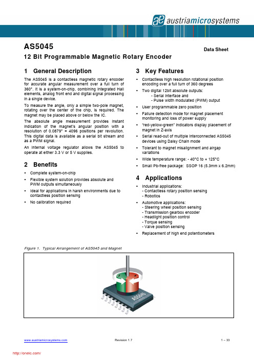
1 General DescriptionThe AS5045 is a contactless magnetic rotary encoder for accurate angular measurement over a full turn of 360°. It is a system-on-chip, combining integrated Hall elements, analog front end and digital signal processing in a single device.To measure the angle, only a simple two-pole magnet, rotating over the center of the chip, is required. The magnet may be placed above or below the IC.The absolute angle measurement provides instant indication of the magnet’s angular position with a resolution of 0.0879° = 4096 positions per revolution. This digital data is available as a serial bit stream and as a PWM signal.An internal voltage regulator allows the AS5045 to operate at either 3.3 V or 5 V supplies.2 BenefitsComplete system-on-chipFlexible system solution provides absolute andPWM outputs simultaneously Ideal for applications in harsh environments due tocontactless position sensing No calibration required3 Key FeaturesContactless high resolution rotational positionencoding over a full turn of 360 degrees Two digital 12bit absolute outputs:- Serial interface and- Pulse width modulated (PWM) output User programmable zero positionFailure detection mode for magnet placementmonitoring and loss of power supply “red-yellow-green” indicators display placement ofmagnet in Z-axis Serial read-out of multiple interconnected AS5045devices using Daisy Chain mode Tolerant to magnet misalignment and airgapvariations Wide temperature range: - 40°C to + 125°CSmall Pb-free package: SSOP 16 (5.3mm x 6.2mm)4 ApplicationsIndustrial applications:- Contactless rotary position sensing - Robotics Automotive applications:- Steering wheel position sensing - Transmission gearbox encoder - Headlight position control - Torque sensing- Valve position sensing Replacement of high end potentiometersFigure 1. Typical Arrangement of AS5045 and MagnetAS504512 Bit Programmable Magnetic Rotary Encoder Data SheetTable of Contents1General Description (1)2Benefits (1)3Key Features (1)4Applications (1)5Pinout (4)5.1Pin Configuration (4)5.2Pin Description (4)6Electrical Characteristics (5)6.1AS5045 Differences to AS5040 (5)6.2Absolute Maximum Ratings (non operating) (6)6.3Operating Conditions (6)6.4DC Characteristics for Digital Inputs and Outputs (7)6.4.1CMOS Schmitt-Trigger Inputs: CLK, CSn. (CSn = internal Pull-up) (7)6.4.2CMOS / Program Input: Prog (7)6.4.3CMOS Output Open Drain: MagINCn, MagDECn (7)6.4.4CMOS Output: PWM (7)6.4.5Tristate CMOS Output: DO (8)6.5Magnetic Input Specification (8)6.6Electrical System Specifications (9)6.7Timing Characteristics (10)6.7.1Synchronous Serial Interface (SSI) (10)6.7.2Pulse Width Modulation Output (11)6.8Programming Conditions (11)7Functional Description (12)8Mode Input Pin (13)8.1Synchronous Serial Interface (SSI) (13)8.1.1Data Content (14)8.1.2Z-axis Range Indication (Push Button Feature, Red/Yellow/Green Indicator) (14)8.2Daisy Chain Mode (15)9Pulse Width Modulation (PWM) Output (16)9.1Changing the PWM Frequency (17)10Analog Output (17)11Programming the AS5045 (18)11.1Zero Position Programming (18)11.2Repeated OTP Programming (18)11.3Non-permanent Programming (19)11.4Analog Readback Mode (20)12Alignment Mode (21)13 3.3V / 5V Operation (22)14Choosing the Proper Magnet (23)14.1Physical Placement of the Magnet (24)15Simulation Modeling (25)16Failure Diagnostics (26)16.1Magnetic Field Strength Diagnosis (26)16.2Power Supply Failure Detection (26)17Angular Output Tolerances (26)17.1Accuracy (26)17.2Transition Noise (28)17.3High Speed Operation (28)17.3.1Sampling Rate (28)17.4Propagation Delays (29)17.4.1Angular Error Caused by Propagation Delay (29)17.5Internal Timing Tolerance (29)17.6Temperature (30)17.6.1Magnetic Temperature Coefficient (30)17.7Accuracy over Temperature (30)17.7.1Timing Tolerance over Temperature (30)18Package Drawings and Markings (31)19Ordering Information (31)20Recommended PCB Footprint (32)5 Pinout5.1 Pin ConfigurationFigure 2. Pin Configuration SSOP165.2 Pin DescriptionTable 1 shows the description of each pin of the standard SSOP16 package (Shrink Small Outline Package, 16 leads, body size: 5.3mm x 6.2mmm; see Figure 2).Pins 7, 15 and 16 supply pins, pins 3, 4, 5, 6, 13 and 14 are for internal use and must not be connected.Pins 1 and 2 MagINCn and MagDECn are the magnetic field change indicators (magnetic field strength increase or decrease through variation of the distance between the magnet and the device). These outputs can be used to detect the valid magnetic field range. Furthermore those indicators can also be used for contact-less push-button functionality.Pin 6 Mode allows switching between filtered (slow) and unfiltered (fast mode). This pin must be tied to VSS or VDD5V, and must not be switched after power up. See chapter 8 Mode Input Pin.Pin 8 Prog is used to program the zero-position into the OTP (see chapter 11.1 Zero Position Programming).This pin is also used as digital input to shift serial data through the device in Daisy Chain configuration, (see chapter 8.2 Daisy Chain Mode).Pin 11 Chip Select (CSn; active low) selects a device within a network of AS5045 encoders and initiates serial data transfer. A logic high at CSn puts the data output pin (DO) to tri-state and terminates serial data transfer. This pin is also used for alignment mode (Figure 14) and programming mode (Figure 10).Pin 12 PWM allows a single wire output of the 10-bit absolute position value. The value is encoded into a pulse width modulated signal with 1µs pulse width per step (1µs to 4096µs over a full turn). By using an external low pass filter, the digital PWM signal is converted into an analog voltage, making a direct replacement of potentiometers possible.Table 1. Pin DescriptionPin Symbol Type Description1MagINCn DO_OD Magnet Field Mag nitude INC rease; active low, indicates a distance reduction between the magnet and the device surface. See Table 52MagDECn DO_OD Magnet Field Mag nitude DEC rease; active low, indicates a distance increase between the device and the magnet. See Table 53 NC - Must be left unconnected4 NC - Must be left unconnectedPin Symbol Type Description 5 NC - Must be left unconnected6Mode - Select between slow (low, VSS) and fast (high, VDD5V) mode. Internal pull-down resistor.7 VSS S Negative Supply Voltage (GND)8Prog_DI DI_PD OTP Prog ramming Input and Data Input for Daisy Chain mode. Internal pull-down resistor (~74kΩ). Connect to VSS if not used9 DO DO_TD ata O utput of Synchronous Serial Interface10 CLK DI,ST Cl oc k Input of Synchronous Serial Interface; Schmitt-Trigger input11 CSn DI_PU,STC hip S elect, active low; Schmitt-Trigger input, internal pull-up resistor (~50kΩ)12 PWM DO P ulse W idth M odulation of approx. 244Hz; 1µs/step (opt. 122Hz; 2µs/step)13 NC - Must be left unconnected14 NC - Must be left unconnected15VDD3V3 S 3V-Regulator Output, internally regulated from VDD5V. Connect to VDD5V for 3V supply voltage. Do not load externally.16 VDD5V S Positive Supply Voltage, 3.0 to 5.5 VDO_OD digital output open drain S supply pinDO digital output DI digital inputDI_PD digital input pull-down DO_T digital output /tri-stateDI_PU digital input pull-up ST Schmitt-Trigger input6 Electrical Characteristics6.1 AS5045 Differences to AS5040All parameters are according to AS5040 datasheet except for the parameters shown below: Building Block AS5045 AS5040Resolution 12bits, 0.088°/step. 10bit, 0.35°/stepData length Read: 18bits(12bits data + 6 bits status)OTP write: 18 bits(12bits zero position + 6 bits mode selection) Read: 16bits(10bits data + 6 bits status)OTP write: 16 bits(10bits zero position + 6 bits mode selection)Incremental encoder Not usedPin 3: not usedPin 4:not usedQuadrature, step/direction and BLDC motorcommutation modesPin 3:incremental output A_LSB_UPin 4:incremental output B_DIR_VPins 1 and 2 MagINCn, MagDECn: same feature asAS5040, additional OTP option for red-yellow-green magnetic range MagINCn, MagDECn indicate in-range or out-of-range magnetic field plus movement of magnet in z-axisPin 6 MODE pin, switch between fast and slowmodePin 6:Index outputPin 12 PWM output: frequency selectable by OTP:1µs / step, 4096 steps per revolution,f=244Hz 2µs/ step, 4096 steps perrevolution, f=122Hz PWM output:1µs / step, 1024 steps per revolution, 976Hz PWM frequencySampling frequency Selectable by MODE input pin:2.5kHz, 10kHzFixed at 10kHz @10bit resolutionBuilding Block AS5045AS5040 Propagation delay 384µs (slow mode) 96µs (fast mode)48µs Transition noise (rms; 1sigma) 0.03 degrees max. (slow mode) 0.06 degrees max. (fast mode)0.12 degreesOTP programming options Zero position, rotational direction, PWMdisable, 2 Magnetic Field indicator modes, 2 PWM frequenciesZero position, rotational direction, incremental modes, index bit width6.2 Absolute Maximum Ratings (non operating)Stresses beyond those listed under “Absolute Maximum Ratings“ may cause permanent damage to the device. These are stress ratings only. Functional operation of the device at these or any other conditions beyond those indicated under “Operating Conditions” is not implied. Exposure to absolute maximum rating conditions for extended periods may affect device reliability. ParameterSymbol Min Max Unit Note DC supply voltage at pin VDD5V VDD5V -0.3 7 V DC supply voltage at pin VDD3V3 VDD3V35VInput pin voltageV in -0.3VDD5V+0.3 V Except VDD3V3 Input current (latchup immunity) I scr -100 100 mA Norm: JEDEC 78Electrostatic discharge ESD ± 2 kV Norm: MIL 883 E method 3015 Storage temperature T strg-55125°CMin – 67°F ; Max +257°FBody temperature (Lead-free package)T Body 260°C t=20 to 40s,Norm: IPC/JEDEC J-Std-020 Lead finish 100% Sn “matte tin” Humidity non-condensing H585%6.3 Operating ConditionsParameterSymbol Min Typ Max UnitNoteAmbient temperature T amb -40125 °C -40°F…+257°FSupply currentI supp 1621 mA Supply voltage at pin VDD5V Voltage regulator output voltage at pin VDD3V3VDD5V VDD3V3 4.53.0 5.03.3 5.5 3.6 V 5V operationSupply voltage at pin VDD5V Supply voltage at pin VDD3V3 VDD5V VDD3V33.03.03.33.33.6 3.6V3.3V operation(pin VDD5V and VDD3V3 connected)6.4 DC Characteristics for Digital Inputs and Outputs6.4.1 CMOS Schmitt-Trigger Inputs: CLK, CSn. (CSn = internal Pull-up)(operating conditions: T amb = -40 to +125°C, VDD5V = 3.0-3.6V (3V operation) VDD5V = 4.5-5.5V (5V operation) unless otherwise noted) ParameterSymbol Min Max Unit NoteHigh level input voltage V IH 0.7 * VDD5VV Normal operation Low level input voltage V IL0.3 * VDD5VVSchmitt Trigger hysteresis V Ion- V Ioff 1V-1 1 CLK only Input leakage current Pull-up low level input current I LEAK I iL-30 -100µA µA CSn only, VDD5V: 5.0V6.4.2 CMOS / Program Input: Prog(operating conditions: T amb = -40 to +125°C, VDD5V = 3.0-3.6V (3V operation) VDD5V = 4.5-5.5V (5V operation)unless otherwise noted) ParameterSymbol Min Max Unit Note High level input voltage VIH 0.7 * VDD5VVDD5VVHigh level input voltage VPROG See Programming ConditionsV During programming Low level input voltage VIL 0.3 * VDD5VVHigh level input current IiL30100µAVDD5V: 5.5V6.4.3 CMOS Output Open Drain: MagINCn, MagDECn(operating conditions: T amb = -40 to +125°C, VDD5V = 3.0-3.6V (3V operation) VDD5V = 4.5-5.5V (5V operation)unless otherwise noted) ParameterSymbolMinMax UnitNote Low level output voltage V OL VSS+0.4 V Output currentI O4 2mAVDD5V: 4.5V VDD5V: 3VOpen drain leakage current I OZ 1 µA6.4.4 CMOS Output: PWM(operating conditions: T amb = -40 to +125°C, VDD5V = 3.0-3.6V (3V operation) VDD5V = 4.5-5.5V (5V operation)unless otherwise noted) ParameterSymbolMinMax UnitNoteHigh level output voltage V OH VDD5V-0.5 V Low level output voltage V OL VSS+0.4 V Output current I O4 2mA mAVDD5V: 4.5V VDD5V: 3V6.4.5 Tristate CMOS Output: DO(operating conditions: T amb = -40 to +125°C, VDD5V = 3.0-3.6V (3V operation) VDD5V = 4.5-5.5V (5V operation) unless otherwise noted) ParameterSymbolMinMax UnitNoteHigh level output voltage V OH VDD5V –0.5VLow level output voltage V OL VSS+0.4 VOutput currentI O4 2mAmAVDD5V: 4.5V VDD5V: 3VTri-state leakage current I OZ 1 µA6.5 Magnetic Input Specification(operating conditions: T amb = -40 to +125°C, VDD5V = 3.0-3.6V (3V operation) VDD5V = 4.5-5.5V (5V operation)unless otherwise noted)Two-pole cylindrical diametrically magnetised source: ParameterSymbolMinTypMaxUnitNoteDiameter d mag 4 6 mm Thickness t mag 2.5 mm Recommended magnet: Ø 6mm x 2.5mm forcylindrical magnets Magnetic input fieldamplitude B pk 4575 mTRequired vertical component of the magnetic field strength on the die’s surface, measured along a concentric circle with a radius of 1.1mm Magnetic offset B off ± 10mT Constant magnetic stray field Field non-linearity5 %Including offset gradient2.44146 rpm @ 4096 positions/rev.; fast modeInput frequency (rotational speed of magnet)f mag_abs0.61Hz36.6rpm @ 4096 positions/rev.; slow mode Displacement radiusDisp0.25mmMax. offset between defined device center and magnet axis (see Figure 18) Eccentricity Ecc 100µm Eccentricity of magnet center to rotational axis-0.12NdFeB (Neodymium Iron Boron) Recommended magnetmaterial andtemperature drift -0.035%/KSmCo (Samarium Cobalt)6.6 Electrical System Specifications(operating conditions: T amb = -40 to +125°C, VDD5V = 3.0~3.6V (3V operation) VDD5V = 4.5~5.5V (5V operation) unless otherwise noted) ParameterSymbolMinTypMaxUnitNoteResolution RES 12 bit 0.088 deg Integral non-linearity (optimum)INL opt± 0.5 deg Maximum error with respect to the best line fit. Centered magnet without calibration, T amb =25 °C. Integral non-linearity (optimum)INL temp± 0.9 degMaximum error with respect to the best line fit. Centered magnetwithout calibration, T amb = -40 to +125°CIntegral non-linearity INL ± 1.4 degBest line fit =(Err max – Err min ) / 2Over displacement tolerance with 6mm diameter magnet, without calibration,T amb = -40 to +125°C Differential non-linearity DNL ±0.044 deg 12bit, no missing codes 0.06 1 sigma, fast mode (MODE = 1)Transition noiseTN0.03deg RMS1 sigma, slow mode (MODE=0 or open)Power-on reset thresholds On voltage; 300mV typ. hysteresisOff voltage; 300mV typ. hysteresisV on V off 1.37 1.08 2.2 1.9 2.9 2.6VDC supply voltage 3.3V (VDD3V3)DC supply voltage 3.3V (VDD3V3)20Fast mode (Mode = 1); until status bit OCF = 1Power-up timet PwrUp80msSlow mode (Mode = 0 or open); until OCF = 196Fast mode (MODE=1)System propagation delay absolute output : delay of ADC, DSP and absolute interfacet delay384µsSlow mode (MODE=0 or open) 2.48 2.61 2.74T amb = 25°C, slow mode (MODE=0 or open)Internal sampling rate for absolute output:f S2.35 2.61 2.87 kHzT amb = -40 to +125°C, slow mode (MODE=0 or open) 9.90 10.42 10.94T amb = 25°C, fast mode (MODE = 1)Internal sampling rate forabsolute outputf S9.38 10.42 11.46kHz T amb = -40 to +125°C, : fast mode (MODE = 1)Read-out frequency CLK1MHz Max. clock frequency to read out serial dataFigure 3. Integral and Differential Non-linearity (example)Integral Non-Linearity (INL) is the maximum deviation between actual position and indicated position. Differential Non-Linearity (DNL) is the maximum deviation of the step length from one position to the next. Transition Noise (TN) is the repeatability of an indicated position6.7 Timing Characteristics6.7.1Synchronous Serial Interface (SSI)(operating conditions: T amb = -40 to +125°C, VDD5V = 3.0~3.6V (3V operation) VDD5V = 4.5~5.5V (5V operation) unless otherwise noted) ParameterSymbol MinTypMaxUnitNoteData output activated (logic high)t DO active 100 nsTime between falling edge of CSn and dataoutput activated First data shifted to output registert CLK FE500 nsTime between falling edge of CSn and firstfalling edge of CLKStart of data output T CLK / 2 500nsRising edge of CLK shifts out one bit at a timeData output valid t DO valid357 375 394 nsTime between rising edge of CLK and dataoutput validData output tristate t DO tristate100 nsAfter the last bit DO changes back to“tristate”Pulse width of CSn t CSn 500ns CSn = high; To initiate read-out of next angular position Read-out frequencyf CLK>01MHzClock frequency to read out serial data分销商库存信息:AMSAS5045-ASST AS5045-ASSU AS5045 PB AS5045 DB V2AS5045 AB。


2SC系列三极管参数2SC系列三极管参数2SC系列三极管参数2SC1000 SI-N 55V 0.1A 0.2W 80MHz2SC1008 SI-N 80V 0.7A 0.8W 75MHz | 2SC1012A SI-N 250V 60mA0.75W >80MHz2SC1014 SI-N 50V 1.5A 7W | 2SC1017 SI-N 75V 1A 60mW 120MHz2SC1030 SI-N 150V 6A 50W | 2SC1046 SI-N 1000V 3A 25W2SC1047 SI-N 30V 20mA 0.4W 650MHz | 2SC1050 SI-N 300V 1A 40W2SC1051 SI-N 150V 7A 60W 8MHz | 2SC1061 SI-N 50V 3A 25W 8MHz=H1062SC1070 SI-N 30V 20mA 900MHz | 2SC1080 SI-N 110V 12A100W 4MHz2SC109 SI-N 50V 0.6A 0.6W | 2SC1096 SI-N 40V 3A 10W60MHz2SC1106 SI-N 350V 2A 80W | 2SC1114 SI-N 300V 4A 100W 10MHz2SC1115 SI-N 140V 10A 100W 10MHz | 2SC1116 SI-N 180V 10A 100W 10MHz 2SC1161 SI-P 160V 12A 120W | 2SC1162 SI-N 35V 1.5A 10W 180MHz2SC1172 SI-N 1500V 5A 50W | 2SC1195 SI-N 200V 2.5A 100W2SC1213C SI-N 50V 0.5A 0.4W UNI | 2SC1214 SI-N 50V 0.5A 0.6W 50MHz2SC1215 SI-N 30V 50mA 0.4W 1.2GHZ | 2SC1216 SI-N 40V 0.2A0.3W <20/402SC1226 SI-N 40/50V 2A 10W 150MHz | 2SC1238 SI-N 35V 0.15A 5W 1.7GHz 2SC1247A SI-N 50V 0.5A 0.4W 60MHz | 2SC1308 SI-N 1500V 7A 50W2SC1312 SI-N 35V 0.1A 0.15W 100MHz | 2SC1318 SI-N 60V 0.5A0.6W 200MHz2SC1343 SI-N 150V 10A 100W 14MHz | 2SC1345 SI-N 55V 0.1A0.1W 230MHz2SC1359 SI-N 30V 30mA 0.4W 250MHz | 2SC1360 SI-N 50V 0.05A 1W >300MHz 2SC1362 SI-N 50V 0.2A 0.25W 140MHz | 2SC1368 SI-N 25V 1.5A 8W 180MHz 2SC1382 SI-N 80V 0.75A 5W 100MHz | 2SC1384 SI-N 60V 1A 1W 200MHz2SC1393 SI-N 30V 20mA 250 mW 700MHz | 2SC1398 SI-N 70V 2A15W2SC1413A SI-N 1200V 5A 50W | 2SC1419 SI-N 50V 2A 20W5MHz2SC1426 SI-N 35V 0.2A 2.7GHz | 2SC1431 SI-N 110V 2A 23W80MHz2SC1432 N-DARL 30V 0.3A 0.3W B=40 | 2SC1439 SI-N 150V 50mA 0.5W 130MHz 2SC1445 SI-N 100V 6A 40W 10MHz | 2SC1446 SI-N 300V 0.1A10W 55MHz2SC1447 SI-N 300V 0.15A 20W 80MHz | 2SC1448 SI-N 150V 1.5A 25W 3MHz2SC1449 SI-N 40V 2A 5W 60MHz | 2SC1450 SI-N 150V 0.4A 20W2SC1454 SI-N 300V 4A 50W 10MHz | 2SC1474-4 SI-N 20V 2A 0.75W 80MHz2SC1501 SI-N 300V 0.1A 10W 55MHz | 2SC1505 SI-N 300V 0.2A15W2SC1507 SI-N 300V 0.2A 15W 80MHz | 2SC1509 SI-N 80V 0.5A 1W 120MHz2SC1515 SI-N 200V 0.05A 0.2W 110MHz | 2SC1520 SI-N 300V 0.2A 12,5W2SC1545 N-DARL 40V 0.3A 0.3W B=1K | 2SC1567 SI-N 100V 0.5A5W 120MHz2SC1570 SI-N 55V 0.1A 0.2W 100MHz | 2SC1571 SI-N 40V 0.1A0.2W 100MHz2SC1573 SI-N 200V 0.1A 1W 80MHz | 2SC1577 SI-N 500V 8A 80W 7MHz2SC1583 SI-N 50V 0.1A 0.4W 100MHz | 2SC1619 SI-N 100V 6A 50W 10MHz2SC1623 SI-N 60V 0.1A 0.2W 250MHz | 2SC1624 SI-N 120V 1A 15W 30MHz2SC1627 SI-N 80V 0.4A 0.8W 100MHz | 2SC1674 SI-N 30V .02A600MC RF/IF2SC1675 SI-N 50V .03A 0.25W | 2SC1678 SI-N 65V 3A 3W2SC1685 SI-N 60V 0.1A 150MC UNI | 2SC1688 SI-N 50V 30mA0.4W 550MHz2SC1708A SI-N 120V 50mA 0.2W 150MHz | 2SC1729 SI-N 35V 3.5A 16W 500MHz 2SC1730 SI-N 30V 0.05A 1.1GHz UHF | 2SC1740 SI-N 40V 100mA 0.3W2SC1741 SI-N 40V 0.5A 0.3W 250MHz | 2SC1756 SI-N 300V0.2A >50MHz2SC1760 SI-N 100V 1A 7.9W 80MHz | 2SC1775A SI-N 120V 0.05A 0.2W UNI2SC1781 SI-N 50V 0.5A 0.35W | 2SC1815 SI-N 50V 0.15A 0.4W 80MHz2SC1815BL SI-N 60V 0.15A 0.4W B>350 | 2SC1815GR SI-N 60V 0.15A 0.4W B>200 2SC1815Y SI-N 60V 0.15A 0.4W B>120 | 2SC1827 SI-N 100V 4A 30W 10MHz2SC1832 N-DARL 500V 15A 150W B>10 | 2SC1841 SI-N 120V 0.05A 0.5W2SC1844 SI-N 60V 0.1A 0.5W 100MHz | 2SC1845 SI-N 120V 0.05A 0.5W2SC1846 SI-N 120V 0.05A 0.5W | 2SC1847 SI-N 50V 1.5A 1.2W2SC1855 SI-N 20V 20mA 0.25W 550MHz | 2SC1871 SI-N 450V 15A 150W <1/3us2SC1879 N-DARL+D 120V 2A 0.8W B>1 | 2SC1890 SI-N 90V 0.05A 0.3W 200MHz2SC1895 SI-N 1500V 6A 50W 2MHz | 2SC1906 SI-N 19V 0.05A0.3W2SC1907 SI-N 30V 0.05A 1100MHz | 2SC1913 SI-N 150V 1A 15W 120MHz2SC1914 SI-N 90V 50mA 0.2W 150MHz | 2SC1921 SI-N 250V 0.05A 0.6W2SC1922 SI-N 1500V 2.5A 50W | 2SC1923 SI-N 30V 20mA 10mW550MHz2SC1929 SI-N 300V 0.4A 25W 80MHz | 2SC1941 SI-N 160V 50mA 0.8W2SC1944 SI-N 80V 6A PQ=16W | 2SC1945 SI-N 80V 6A 20W2SC1946A SI-N 35V 7A 50W | 2SC1947 SI-N 35V 1A4W/175MHz2SC1953 SI-N 150V 0.05A 1.2W 70MHz | 2SC1957 SI-N 40V 1A1.8W/27MHz2SC1959 SI-N 30V 0.5A 0.5W 200MHz | 2SC1967 SI-N 35V 2A 8W 470MHz2SC1968 SI-N 35V 5A 3W 470MHz | 2SC1969 SI-N 60V 6A 20W2SC1970 SI-N 40V 0.6A 5W | 2SC1971 SI-N 35V 2A 12.5W2SC1972 SI-N 35V 3.5A 25W | 2SC1975 SI-N 120V 2A 3.8W50MHz2SC1980 SI-N 120V 20mA 0.25W 200MHz | 2SC1984 SI-N 100V 3A 30W B=700 2SC1985 SI-N 80V 6A 40W 10MHz | 2SC2023 SI-N 300V 2A 40W 10MHz2SC2026 SI-N 30V 0.05A 0.25W | 2SC2027 SI-N 1500/800V 5A 50W2SC2036 SI-N 80V 1A PQ=1..4W | 2SC2053 SI-N 40V 0.3A 0.6W 500MHz2SC2055 SI-N 18V 0,3A 0,5W | 2SC2058 SI-N 40V 0.05A 0.25W2SC2060 SI-N 40V 0.7A 0.75W 150MHz | 2SC2061 SI-N 80V 1A0.75W 120MHz2SC2068 SI-N 300V 0.05A 95MHz | 2SC2073 SI-N 150V 1.5A 25W 4MHz2SC2078 SI-N 80V 3A 10W 150MHz | 2SC2086 SI-N 75V 1A0.45W/27MHz2SC2092 SI-N 75V 3A 5W 27MHz | 2SC2094 SI-N 40V 3.5A PQ>15W 175MHz 2SC2097 SI-N 50V 15A PQ=85W | 2SC2120 SI-N 30V 0.8A 0.6W 120MHz2SC2122 SI-N 800V 10A 50W | 2SC2166 SI-N 75V 4A 12.5W RFPOWER2SC2168 SI-N 200V 2A 30W 10MHz | 2SC2200 SI-N 500V 7A 40W1US2SC2209 SI-N 50V 1.5A 10W 150MHz | 2SC2216 SI-N 45V 50mA 0.3W 300MHz 2SC2228 SI-N 160V 0.05A 0.75W >50 | 2SC2229 SI-N 200V 50mA 0.8W 120MHz 2SC2230 SI-N 200V 0.1A 0.8W 50MHz | 2SC2233 SI-N 200V 4A 40W 8MHz2SC2235 SI-N 120V 0.8A 0.9W 120MHz | 2SC2236 SI-N 30V 1.5A0.9W 120MHz2SC2237 SI-N 35V 2A PQ>7.5W 175MHz | 2SC2238 SI-N 160V 1.5A 25W 100MHz 2SC2240 SI-N 120V 50mA .3W 100MHz | 2SC2261 SI-N 180V 8A80W 15MHz2SC2267 SI-N 400/360V 0.1A 0.4W | 2SC2270 SI-N 50V 5A 10W 100MHz2SC2271 SI-N 300V 0.1A 0.9W 50MHz | 2SC2275 SI-N 120V 1.5A25W 200MHz2SC2283 SI-N 38V 0.75A 2.8W(500MHz | 2SC2287 SI-N 38V 1.5A 7.1W 175MHz2SC2295 SI-N 30V 0.03A 0.2W 250MHz | 2SC2307 SI-N 500V 12A 100W 18MHz2SC2308 SI-N 55V 0.1A 0.2W 230MHz | 2SC2310 SI-N 55V 0.1A0.2W 230MHz2SC2312 SI-N 60V 6A 18.5W/27MHz | 2SC2314 SI-N 45V 1A 5W2SC2320 SI-N 50V 0,2A 0,3W | 2SC2329 SI-N 38V 0.75A 2W 175MHz2SC2331 SI-N 150V 2A 15W POWER | 2SC2333 SI-N 500/400V 2A 40W2SC2334 SI-N 150V 7A 40W POWER | 2SC2335 SI-N 500V 7A 40W POWER2SC2336B SI-N 250V 1.5A 25W 95MHz | 2SC2344 SI-N 180V 1.5A 25W 120MHz2SC2347 SI-N 15V 50mA 250mW 650MHz | 2SC2362 SI-N 120V50mA 0.4W 130MHz2SC2363 SI-N 120V 50mA 0.5W 130MHz | 2SC2365 SI-N 600V 6A50W POWER2SC2369 SI-N 25V 70mA 0.25W 4.5GHz | 2SC2383 SI-N 160V 1A2SC2389 SI-N 120V 50mA 0.3W 140MHz | 2SC2407 SI-N 35V 0.15A 0.16W 500MHz 2SC2412 SI-N 50V 0.1A 180MHz | 2SC2433 SI-N 120V 30A 150W 80MHz2SC2440 SI-N 450V 5A 40W | 2SC2458 SI-N 50V 0.15A 0.2W 80MHz2SC2466 SI-N 30V 0.05A 2.2GHz | 2SC2482 SI-N 300V 0.1A 0.9W 50MHz2SC2485 SI-N 100V 6A 70W 15MHz | 2SC2486 SI-N 120V 7A 80W 15MHz2SC2491 SI-N 100V 6A 40W 15MHz | 2SC2497 SI-N 70V 1.5A 5W 150MHz2SC2498 SI-N 30V 0.05A 0.3W 3.5GHz | 2SC2508 SI-N 40V 6A 50W 175MHz2SC2510 SI-N 55V 20A 250W(28MHz) | 2SC2512 SI-N 30V 50mA 900MHz TUNE2SC2516 SI-N 150V 5A 30W <0.5/2us | 2SC2517 SI-N 150V 5A 30W <0.5/2us2SC2538 SI-N 40V 0.4A 0.7W | 2SC2539 SI-N 35V 4A 17W175MHz2SC2542 SI-N 450V 5A 40W | 2SC2547 SI-N 120V 0.1A 0.4W2SC2551 SI-N 300V 0.1A 0.4W 80MHz | 2SC2552 SI-N 500V 2A 20W2SC2553 SI-N 500V 5A 40W 1us | 2SC2562 SI-N 60V 5A 25W0.1us2SC2563 SI-N 120V 8A 80W 90MHz | 2SC2570A SI-N 25V 70mA 0.6W2SC2579 SI-N 160V 8A 80W 20MHz | 2SC2581 SI-N 200V 10A100W2SC2590 SI-N 120V 0.5A 5W 250MHz | 2SC2592 SI-N 180V 1A 20W 250MHz2SC2603 SI-N 50V 0.2A 0.3W | 2SC2610 SI-N 300V 0.1A 0.8W 80MHz2SC2611 SI-N 300V 0.1A 0.8W 80MHz | 2SC2621E SI-N 300V 0.2A 10W >50MHz 2SC2625 SI-N 450V 10A 80W | 2SC2630 SI-N 35V 14A 100W2SC2631 SI-N 150V 50mA 0,75W 160MHz | 2SC2632 SI-N 150V 50mA2SC2634 SI-N 60V 0.1A 0.4W 200MHz | 2SC2653 SI-N 350V 0.2A15W >50MHz2SC2654 SI-N 40V 7A 40W | 2SC2655 SI-N 50V 2A 0.9W 0.1us2SC2656 SI-N 450V 7A 80W <1.5/4.5 | 2SC2660 SI-N 200V 2A 30W 30MHz2SC2668 SI-N 30V 20mA 0.1W 550MHz | 2SC2671 SI-N 15V 80mA 0.6W 5.5GHz 2SC2682 SI-N 180V 0.1A 8W 180MHz | 2SC2690 SI-N 120V 1.2A20W 160MHz2SC2694 SI-N 35V 20A 140W | 2SC2705 SI-N 150V 50mA 0.8W 200MHz2SC2706 SI-N 140V 10A 100W 90MHz | 2SC2712 SI-N 50V 0.15A 0.15W 80MHz 2SC2714 SI-N 30V 20mA 0.1W 550MHz | 2SC2717 SI-N 30V 50mA 0.3W 300MHz 2SC2724 SI-N 30V 30mA 200MHz | 2SC2749 SI-N 500V 10A100W 50MHz2SC2750 SI-N 150V 15A 100W POWER | 2SC2751 SI-N 500V 15A 120W 50MHz 2SC2752 SI-N 500V 0.5A 10W <1/3.5 | 2SC2753 SI-N 17V 0.07A0.3W 5GHz2SC2759 SI-N 30V 50mA 0.2W 2.3GHz | 2SC2786 SI-N 20V 20mA 600MHz2SC2787 SI-N 50V 30mA 0.3W 250MHz | 2SC2791 SI-N 900V 5A 100W2SC2792 SI-N 850V 2A 80W | 2SC2793 SI-N 900V 5A 100W2SC2802 SI-N 300V 0.2A 10W 80MHz | 2SC2808 SI-N 100V 50mA 0.5W 140MHz 2SC2810 SI-N 500V 7A 50W 18MHz | 2SC2812 SI-N 55V 0.15A0.2W 100MHz2SC2814 SI-N 30V 0.03A 320MHz F | 2SC2825 SI-N 80V 6A 70W B>5002SC2837 SI-N 150V 10A 100W 70MHz | 2SC2839 SI-N 20V 30mA 0.15W 320MHz 2SC2851 SI-N 36V 0.3A 1W 1.5GHz | 2SC2873 SI-N 50V 2A 0.5W 120MHz2SC2878 SI-N 20V 0.3A 0.4W 30MHz | 2SC2879 SI-N 45V 25APEP=100W 28MHz2SC2882 SI-N 90V 0.4A 0.5W 100MHz | 2SC288A SI-N 35V 20mA 0.15W2SC2898 SI-N 500V 8A 50W | 2SC2901 SI-N 40V 0.2A 0.6W<12/182SC2908 SI-N 200V 5A 50W 50MHz | 2SC2910 SI-N 160V 70mA 0.9W 150MHz2SC2911 SI-N 180V 140mA 10W 150MHz | 2SC2912 SI-N 200V140mA 10W 150MHz2SC2922 SI-N 180V 17A 200W 50MHz | 2SC2923 SI-N 300V 0.1A 140MHz2SC2928 SI-N 1500V 5A 50W | 2SC2939 SI-N 500V 10A 100W 2.5us2SC2958 SI-N 160V 0.5A 1W | 2SC2979 SI-N 800V 3A 40W2SC2987 SI-N 140V 12A 120W 60MHz | 2SC2988 SI-N 36V 0.5A 175MHz2SC2999 SI-N 20V 30mA 750MHz | 2SC3001 SI-N 20V 3APQ=7W(175MHz)2SC3019 SI-N 35V 0.4A 0.6W 520MHz | 2SC3020 SI-N 35V 1A 10W2SC3022 SI-N 35V 7A 50W | 2SC3026 SI-N 1700V 5A 50W POWER2SC3030 N-DARL 900V 7A 80W | 2SC3039 SI-N 500V 7A 52W2SC3042 SI-N 500/400V 12A 100W | 2SC3052F SI-N 50V 0.2A0.15W 200MHz2SC3063 SI-N 300V 0.1A 1.2W 140MHz | 2SC3067 2xSI-N 130V50mA 0.5W 1602SC3068 SI-N 30V 0.3A Ueb=15V B>8 | 2SC3071 SI-N 120V 0.2A Ueb=15V B>2SC3073 SI-N 30V 3A 15W 100MHz | 2SC3074 SI-N 60V 5A 20W 120MHz2SC3075 SI-N 500V 0.8A 10W 1/1.5us | 2SC3089 SI-N 800V 7A 80W2SC3101 SI-N 250V 30A 200W 25MHz | 2SC3102 SI-N 35V 18A 170W 520MHz2SC3112 SI-N 50V 0.15A 0.4W 100MHz | 2SC3116 SI-N 180V 0.7A 10W 120MHz 2SC3117 SI-N 180V 1.5A 10W 120MHz | 2SC3133 SI-N 60V 6A 1.5W27MHz2SC3148 SI-N 900V 3A 40W 1us | 2SC3150 SI-N 900V 3A 50W 15MHz2SC3153 SI-N 900V 6A 100W | 2SC3157 SI-N 150V 10A 60W2SC3158 SI-N 500V 7A 60W | 2SC3164 SI-N 500V 10A 100W2SC3169 SI-N 500V 2A 25W >8MHz | 2SC3175 SI-N 400V 7A 50W 40MHz2SC3178 SI-N 1200V 2A 60W | 2SC3179 SI-N 60V 4A 30W15MHz2SC3180N SI-N 80V 6A 60W 30MHz | 2SC3181N SI-N 120V 8A 80W 30MHz2SC3182N SI-N 140V 10A 100W 30MHz | 2SC3195 SI-N 30V 20mA 0.1W 550MHz2SC3199 SI-N 60V 0.15A 0.2W 130MHz | 2SC3200 SI-N 120V 0.1A 0.3W 100MHz 2SC3202 SI-N 35V 0.5A 0.5W 300MHz | 2SC3203 SI-N 35V 0.8A0.6W 120MHz2SC3205 SI-N 30V 2A 1W 120MHz2SC4544参数:Si-NPN 300V 0.1A 8W 70MHz| 2SC3206 SI-N 150V 0.5A 0.8W 120MHz2SC3210 SI-N 500V 10A 100W 1us | 2SC3211 SI-N 800V 5A70W >3MHz2SC3212 SI-N 800V 7A 3W 3.5MHz | 2SC3225 SI-N 40V 2A 0.9W 1us2SC3231 SI-N 200V 4A 40W 8MHz | 2SC3240 SI-N 50V 25A 110W 30MHz2SC3242 SI-N 20V 2A 0.9W 80MHz | 2SC3244E SI-N 100V 0.5A 0.9W 130MHz2SC3245A SI-N 150V 0.1A 0.9W 200MHz | 2SC3246 SI-N 30V 1.5A 0.9W 130MHz 2SC3247 SI-N 50V 1A .9W 130MHz B> | 2SC3257 SI-N 250V 10A40W 1/3.5us2SC3258 SI-N 100V 5A 30W 120MHz | 2SC3260 N-DARL 800V 3A 50W B>102SC3262 N-DARL 800V 10A 100W | 2SC3263 SI-N 230V 15A130W2SC3264 SI-N 230V 17A 200W 60MHz | 2SC3271 SI-N 300V 1A 5W 80MHz2SC3277 SI-N 500V 10A 90W 20MHz | 2SC3279 SI-N 10V 2A 0.75W 150MHz2SC3280 SI-N 160V 12A 120W 30MHz | 2SC3281 SI-N 200V 15A 150W 30MHz 2SC3284 SI-N 150V 14A 125W 60MHz | 2SC3293 N-DARL+D 50V 1.2A 20W 180 2SC3297 SI-N 30V 3A 15W 100MHz | 2SC3299 SI-N 60V 5A 20W 0.1us2SC3300 SI-N 100V 15A 100W | 2SC3303 SI-N 100V 5A 20W 0.2us2SC3306 SI-N 500V 10A 100W 1us | 2SC3307 SI-N 900V 10A150W 1us2SC3309 SI-N 500V 2A 20W 1us | 2SC3310 SI-N 500V 5A 30W1us2SC3311 SI-N 60V 0.1A 0.3W 150MHz | 2SC3320 SI-N 500V 15A80W2SC3326 SI-N 20V 0.3A 0.15W 30MHz | 2SC3327 SI-N 50V 0.3A0.2W 30MHz2SC3328 SI-N 80V 2A 0.9W 100MHz | 2SC3330 SI-N 60V 0.2A 0.3W 200MHz2SC3331 SI-N 60V 0.2A 0.5W 200MHz | 2SC3332 SI-N 180V 0.7A 0.7W 120MHz 2SC3334 SI-N 250V 50mA 0.9W 100MHz | 2SC3345 SI-N 60V 12A40W 90MHz2SC3346 SI-N 80V 12A 40W 0.2us | 2SC3355 SI-N 20V 0.1A 0.6W 6.5GHz2SC3356 SI-N 20V 0.1A 0.2W 7GHz | 2SC3377 SI-N 40V 1A 0.6W 150MHz2SC3378 SI-N 120V 0.1A 0.2W 100MHz | 2SC3379 SI-N 20V 1.5APQ=3W2SC3381 2xSI-N 80V 0.1A 0.4W 170MHz | 2SC3383 SI-N 60V 0.2A 0.5W 250MHz 2SC3397 SI-N 50V 0.1A 250MHz 46K/ | 2SC3399 SI-N 50V 0.1A250MHz2SC3400 SI-N 50V 0.1A 250MHz 22K/ | 2SC3401 SI-N 50V .1A46K/23KOHM2SC3402 SI-N 50V 0.1A 250MHz 10K/ | 2SC3405 SI-N 900V 0.8A20W 1us2SC3409 SI-N 900V 2A 80W .8uS | 2SC3416 SI-N 200V 0.1A 5W 70MHz2SC3419 SI-N 40V 0.8A 5W 100MHz | 2SC3420 SI-N 50V 5A 10W 100MHz2SC3421O SI-N 120V 1A 1.5W BJT O-G | 2SC3421Y SI-N 120V 1A10W 120MHz2SC3422Y SI-N 40V 3A 10W 100MHz | 2SC3423 SI-N 150V 50mA 5W 200MHz 2SC3425 SI-N 500V 0.8A 10W | 2SC3446 SI-N 800V 7A 40W18MHz2SC3447 SI-N 800V 5A 50W 18MHz | 2SC3456 SI-N 1100/800V 1.5A 40W2SC3457 SI-N 1100V 3A 50W | 2SC3460 SI-N 1100V 6A 100W2SC3461 SI-N 1100/800V 8A 120W | 2SC3466 SI-N 1200/650V 8A 120W2SC3467 SI-N 200V 0.1A 1W 150MHz | 2SC3468 SI-N 300V 0.1A 1W 150MHz2SC3486 SI-N 1500V 6A 120W | 2SC3502 SI-N 200V 0.1A 1.2W2SC3503 SI-N 300V 0.1A 7W 150MHz | 2SC3504 SI-N 70V 0.05A 0.9W 500MHz 2SC3505 SI-N 900V 6A 80W | 2SC3507 SI-N 1000/800V 5A80W2SC3509 N-DARL+D 900V 10A 100W 0. | 2SC3514 SI-N 180V 0.1A 10W 200MHz 2SC3518 SI-N 60V 5A 10W | 2SC3520 SI-N 500V 18A 130W 18MHz2SC3526 SI-N 110V 0.15A 7A 30W 1us | 2SC3528 SI-N 500V 20A 125W2SC3549 SI-N 900V 3A 40W | 2SC3552 SI-N 1100V 12A 150W 15MHz2SC3568 SI-N 150V 10A 30W | 2SC3571 SI-N 500V 7A 30W2SC3577 SI-N 850V 5A 80W 6MHz | 2SC3581 SI-N 55V 0.4A 0.9W 150MHz2SC3591 SI-N 400V 7A 50W | 2SC3595 SI-N 30V 0.5A 5W2SC3596 SI-N 80V 0.3A 8W 700MHz | 2SC3597 SI-N 80V 0.5A 10W 800MHz2SC3599 SI-N 120V 0.3A 8W 500MHz | 2SC3600 SI-N 200V 0.1A 7W 400MHz2SC3601 SI-N 200V 0.15A 7W 400MHz | 2SC3608 SI-N 20V 0.08A 6.5GHz2SC3611 SI-N 50V 0.15A 4W 300MHz | 2SC3616 SI-N 25V 0.7A250MHz2SC3621 SI-N 150V 1.5A 10W 100MHz | 2SC3623 SI-N 60V 0.15A 0.25W B=1K2SC3632 SI-N 600V 1A 10W 30MHz | 2SC3636 SI-N 900/500V 7A 80W2SC3642 SI-N 1200V 6A 100W 200ns | 2SC3655 SI-N 50V 0.1A0.4W 46/23K2SC3656 SI-N 50V 0.1A 0.4W 10K/10 | 2SC3659 SI-N+D 1700/800V 5A 50W2SC3668 SI-N 50V 2A 1W 100MHz | 2SC3669 SI-N 80V 2A 1W 0.2us2SC3675 SI-N 1500/900V 0.1A 10W | 2SC3678 SI-N 900V 3A 80W2SC3679 SI-N 900/800V 5A 100W | 2SC3680 SI-N 900/800V 7A 120W 6MHz2SC3684 SI-N+D 1500V 10A 150W | 2SC3688 SI-N 1500V 10A 150W 0.2us2SC3692 SI-N 100V 7A 30W <300/180 | 2SC373 SI-N 35V 0.1A 0.2W B>2002SC3746 SI-N 80V 5A 20W 100MHz | 2SC3748 SI-N 80V 10A 30W 100/600ns2SC3752 SI-N 1100/800V 3A 30W | 2SC3781 SI-N 120V 0.4A 15W 500MHz2SC3782 SI-N 200V 0.2A 15W 400MHz | 2SC3783 SI-N 800V 5A100W2SC3787 SI-N 180V 0.14A 10W 150MHz | 2SC3788 SI-N 200V 0.1A 5W 150MHz 2SC3789 SI-N 300V 0.1A 7W 70MHz | 2SC3790 SI-N 300V 0.1A 7W 150MHz2SC3792 SI-N 50V 0.5A 0.5W 250MHz | 2SC3795A SI-N 900V 5A2SC3807 SI-N 30V 2A 15W 260MHz | 2SC3808 N-DARL 80V 2A 170MHz B>802SC380TM SI-N 30V 50mA 0.3W 100MHz | 2SC3811 SI-N 40V 0.1A 0.4W 450MHz 2SC3831 SI-N 500V 10A 100W | 2SC3833 SI-N 500/400V 12A 100W2SC3842 SI-N 600V 10A 70W 32MHz | 2SC3844 SI-N 600V 15A75W 30MHz2SC3851 SI-N 80V 4A 25W 15MHz | 2SC3852 SI-N 80V 3A 25W 15MHz2SC3855 SI-N 200V 10A 100W 20MHz | 2SC3857 SI-N 200V 15A 150W 20MHz2SC3858 SI-N 200V 17A 200W 20MHz | 2SC3866 SI-N 900V 3A 40W2SC3868 SI-N 500V 1.5A 25W 0.7us | 2SC3883 SI-N+D 1500V 6A 50W2SC3884A SI-N 1500V 6A 50W | 2SC3886A SI-N 1500V 8A 50W 0.1us2SC388A SI-N 25V 50mA 0.3W 300MHz | 2SC3890 SI-N 500V 7A30W 500NS2SC3892A SI-N+D 1500V 7A 50W 0.4us | 2SC3893A SI-N+D 1500V8A 50W2SC3895 SI-N 1500/800V 8A 70W | 2SC3896 SI-N 1500V 8A 70W2SC3897 SI-N 1500V 10A 70W | 2SC3902 SI-N 180V 1.5A 10W 120MHz2SC3907 SI-N 180V 12A 130W 30MHz | 2SC3927 SI-N 900V 10A 120W2SC394 SI-N 25V 0.1A 200MC RF | 2SC3940 SI-N 30V 1A 1W200MHz2SC3943 SI-N 110V 0.15A 2W 300MHz | 2SC3944 SI-N 150V 1A 40W 300MHz 2SC3948 SI-N 850V 10A 75W 20MHz | 2SC3950 SI-N 30V 0.5A 5W2SC3952 SI-N 80V 0.5A 10W 700MHz | 2SC3953 SI-N 120V 0.2A 8W 400MHz2SC3954 SI-N 120V 0.3A 8W 400MHz | 2SC3955 SI-N 200V 0.1A 7W 300MHz2SC3956 SI-N 200V 0.2A 7W 70MHz | 2SC3964 SI-N 40V 2A 1.5W2SC3972 SI-N 800/500V 5A 40W | 2SC3973A SI-N 900V 7A 45W2SC3979A SI-N 800V 3A 2W 10MHz | 2SC3987 N-DARL+D 50V 3A 15W2SC3996 SI-N 1500/800V 15A 180W | 2SC3998 SI-N 1500V 25A 250W POWER 2SC3999 SI-N 300V 0.1A 0.75W 300MHz | 2SC4004 SI-N 900/800V 1A 30W <1/4 2SC4020 SI-N 900V 3A 50W 1us | 2SC4024 SI-N 100V 10A 35W B>3002SC4029 SI-N 230V 15A 150W 30MHz | 2SC4043 SI-N 20V 50mA 0.15W 3.2GHz 2SC4046 SI-N 120V 0.2A 8W 350MHz | 2SC4052 SI-N 600V 3A 40W 20MHz2SC4056 SI-N 600V 8A 45W | 2SC4059 SI-N 600/450V 15A 130W2SC4064 SI-N 50V 12A 35W 40MHz | 2SC4107 SI-N 500/400V 10A 60W2SC4119 N-DARL+D 1500V 15A 250W B | 2SC4123 SI-N+D 1500V 7A 60W2SC4125 SI-N+D 1500/800V 10A 70W | 2SC4131 SI-N 100V 15A60W 18MHz2SC4135 SI-N 120V 2A 15W 200MHz | 2SC4137 SI-N 25V 0.1A300MHz2SC4138 SI-N 500V 10A 80W <1/3.5us | 2SC4153 SI-N 200V 7A 30W 0.5us2SC4157 SI-N 600V 10A 100W | 2SC4159 SI-N 180V 1.5A 15W 100MHz2SC4161 SI-N 500V 7A 30W | 2SC4169 N-DARL+D 50V 1.2A1W B=4K2SC4199 SI-N 1400V 10A 100W | 2SC4200 SI-N 20V 0.6A 5W 2.5GHz2SC4204 SI-N 30V 0.7A 0.6W | 2SC4231 SI-N 1200/800V 2A30W2SC4235 SI-N 1200/800V 3A 80W | 2SC4236 SI-N 1200/800V 6A 100W2SC4237 SI-N 1200/800V 10A 150W | 2SC4242 SI-N 450/400V 7A2SC4256 SI-N 1500V 10A 175W 6MHz | 2SC4278 SI-N 150V 10A 100W 30MHz 2SC4288A SI-N1600/600V 12A 200W | 2SC4289A SI-N 1500V 16A 200W2SC4290A SI-N 1500V 20A 200W | 2SC4297 SI-N 500V 12A 75W 10MHz2SC4298 SI-N 500V 15A 80W 10MHz | 2SC4300 SI-N 900V 5A 75W 1/6us2SC4304 SI-N 800V 3A 35W | 2SC4308 SI-N 30V 0.3A 0.6W 2.5GHz2SC4313 SI-N 900V 10A 100W 0.5us | 2SC4381 SI-N 150V 2A 25W 15MHz2SC4382 SI-N 200V 2A 25W 15MHz | 2SC4386 SI-N 160/120V 8A 75W 20MHz 2SC4387 SI-N 200V 10A 80W 20MHz | 2SC4388 SI-N 200V 15A85W 20MHz2SC4408 SI-N 80V 2A 0.9W 100/600ns | 2SC4429 SI-N 1100/800V 8A 60W2SC4430 SI-N 1100V 12A 65W 15MHz | 2SC4431 SI-N 120V 1.5A 20W 150MHz 2SC4439 SI-N 180V 0.3A 8W 400MHz | 2SC4467 SI-N 160/120V 8A 80W 20MHz 2SC4468 SI-N 200V 10A 80W 20MHz | 2SC4484 SI-N 30V 2.5A 1W 250MHz2SC4488 SI-N 120V 1A 1W 120MHz | 2SC4511 SI-N 120V 6A 30W 20MHz2SC4512 SI-N 120V 6A 50W 20MHz | 2SC4517 SI-N 900V 3A 30W 6MHz2SC4517A SI-N 1000V 3A 30W 0.5us | 2SC4531 SI-N+D 1500V 10A 50W2SC4532 SI-N 1700V 10A 200W 2uS | 2SC4538 SI-N 900V 5A 80W2SC454 SI-N 30V 0.1A 230MHz | 2SC4542 SI-N 1500V 10A 50W2SC4547 N-DARL+D 85V 3A 30W B>2K | 2SC4557 SI-N 900V 10A 80W <1/5.5us 2SC4560 SI-N 1500V 10A 80W | 2SC458 SI-N 30V 0.1A 230MC UNI0.2W 230MHz2SC461 SI-N 30V 0.1A 0.2W 230MHz | 2SC4744 SI-N 1500V 6A POWER2SC4745 SI-N 1500V 6A | 2SC4747 SI-N 1500V 10A 50W0.3us2SC4758 SI-N 1500V 8A 50W HI-RES | 2SC4769 SI-N+D 1500V 7A 60W2SC4770 SI-N 1500/800V 7A 60W | 2SC4793 SI-N 230V 1A 2W 100MHz2SC4804 SI-N 900V 3A 30W 0.3us | 2SC4820 SI-N 450V 6A 30W 12MHz2SC4826 SI-N 200V 3A 1.3W 300MHz | 2SC4834 SI-N 500V 8A 45W <0.3/1.42SC4883A SI-N 180V 2A 20W 120MHz | 2SC4891 SI-N 1500V 15A 75W2SC4908 SI-N 900V 3A 35W 1us | 2SC4924 SI-N 800V 10A 70W2SC4977 SI-N 450V 7A 40W | 2SC5002 SI-N 1500V 7A 80W2SC5003 SI-N+D 1500V 7A 80W | 2SC5027 SI-N 1100V 3A 50W 0.3us2SC5030 SI-N 50V 5A 1.3W 150MHz | 2SC5045 SI-N 1600V 15A75W2SC5047 SI-N 1600V 25A 250W | 2SC5048 SI-N 1500V 12A 50W 0.3us2SC5070 SI-N 30V 2A 1.5W B>800 | 2SC5086 SI-N 20V 80MA7GHZ2SC509 SI-N 35V 0.5A 0.6W 60MHz | 2SC5144 SI-N 1700V 20A 200W2SC5148 SI-N 1500V 8A 50W 0.2us | 2SC5149 SI-N+D 1500V 8A 50W 0.2us 2SC5150 SI-N 1700V 10A 50W 03us | 2SC5171 SI-N 180V 2A 20W 200MHz 2SC5198 SI-N 140V 10A 100W 30MHz | 2SC5207 SI-N 1500V 10A 50W 0.4us 2SC5242 SI-N 230V 15A 130W 30MHz | 2SC5244A SI-N 1600V 30A 200W2SC5296 SI-N+D 1500V 8A 60W | 2SC5297 SI-N 1500V 8A 60W0.1W 0.700M2SC536 SI-N 40V 0.1A 180MC UNI | 2SC620 SI-N 50V 0.2A 0.25W UNI2SC643 SI-N 1100V 2.5A 50W | 2SC644 SI-N 30V 50mA 0.25W2SC645 SI-N 30V 30mA 0.14W 200MHz | 2SC710 SI-N 30V 0.03A 200MHz2SC711 SI-N 30V 0.05A 150MHz | 2SC712 SI-N 30V 0.5A150MHz2SC717 SI-N 30V 50mA 0.2W 600MHz | 2SC730 SI-N 40V 0.4APQ=1.5W2SC732 SI-N 50V 0.15A 0.4W 150MHz | 2SC735 SI-N 35V 0.4A 0.3W UNI2SC752 SI-N 15V 100mA 0.1W | 2SC756 SI-N 40V 4A 10W65MHz2SC784 SI-N 40V 0.02A 500MC RF | 2SC815 SI-N 60V 0.2A 0.25W 200MHz 2SC828 SI-N 30V 0.05A 0.25W UNI | 2SC829 SI-N 30V 30mA 0.4W 230MHz 2SC839 SI-N 50V 0.03A 250MHz | 2SC867 SI-N 400V 1A 23W8MHz2SC869 SI-N 160V 30mA 0.2W 150MHz | 2SC898A SI-N 150V 7A80W 15MHz2SC900 SI-N 30V 0.03A 100MHz | 2SC930 SI-N 15V 0.03A300MC RF2SC936 SI-N 1000V 1A 22W POWER | 2SC941 SI-N 35V 20mA 0.2W 120MHz 2SC943 SI-N 60V 0.2A 0.3W 220MHz | 2SC945 SI-N 50V 0.1A250MC UNI2SC982 N-DARL 40V 0.3A 0.4W。