MAX6347XR44-T中文资料
- 格式:pdf
- 大小:159.68 KB
- 文档页数:8


M A X471M A X472的中文资料大全(总4页)-本页仅作为预览文档封面,使用时请删除本页-MAX471/MAX472的特点、功能美国美信公司生产的精密高端电流检测放大器是一个系列化产品,有MAX471/MA X472、 MAX4172/MAX4173等。
它们均有一个电流输出端,可以用一个电阻来简单地实现以地为参考点的电流/电压的转换,并可工作在较宽电压内。
MAX471/MAX472具有如下特点:●具有完美的高端电流检测功能;●内含精密的内部检测电阻(MAX471);●在工作温度范围内,其精度为2%;●具有双向检测指示,可监控充电和放电状态;●内部检测电阻和检测能力为3A,并联使用时还可扩大检测电流范围;●使用外部检测电阻可任意扩展检测电流范围(MAX472);●最大电源电流为100μA;●关闭方式时的电流仅为5μA;●电压范围为3~36V;●采用8脚DIP/SO/STO三种封装形式。
MAX471/MAX472的引脚排列如图1所示,图2所示为其内部功能框图。
表1为MAX471/MAX472的引脚功能说明。
MAX471的电流增益比已预设为500μA/A,由于2kΩ的输出电阻(ROUT)可产生1V/A的转换,因此±3A时的满度值为3V.用不同的ROUT电阻可设置不同的满度电压。
但对于MAX471,其输出电压不应大于VRS+。
对于MAX472,则不能大于。
MAX471引脚图如图1所示,MAX472引脚图如图2所示。
MAX471/MAX472的引脚功能说明引脚名称功能MAX471MAX47211SHDN关闭端。
正常运用时连接到地。
当此端接高电平时,电源电流小于5μA2,3-RS+内部电流检测电阻电池(或电源端)。
“+”仅指示与SIGN输出有关的流动方向。
封装时已将2和3连在了一起-2空脚-3RG1增益电阻端。
通过增益设置电阻连接到电流检测电阻的电池端44GND地或电池负端55SIGN集电极开路逻辑输出端。

A3 BAP64-03 Phi I SOD323 3 GHz pin diodeA3 HSMS-2803 HP D SOT23 HP2800 ser pairA3 MMBD1005 Mot A SOT23 dual ca Si diode low leakage A3 BAS16 Zet C Si sw 75V 100mAA3 BAT17 Phi C SOT23 BA481A3p BAT17 Phi C SOT23 BA481A3t BAT17 Phi C SOT23 BA481A3 MBT3906DW Mot N SOT363 dual 2N3906A3X MMBD2835 Mot A SOT23 dual ca sw 35V 100 mA 15nS A4 HSMS-2804 HP B SOT23 dual cc HP2800 schottkyA4s BAV70W Sie B SOT323 dual cc BAW62A4s BAV70 Sie B SOT23 dual cc BAW62A4s BAV70TSie B SOT416 dual cc BAW62_________________A4s BAV70U Sie B SC74 dual cc BAW62BAV70W Phi B SOT323 dual cc BAW62A4 qA4p BAV70 Phi B SOT23 dual cc BAW62A4t BAV70 Phi B SOT23 dual cc BAW62A4t BAV70 Phi B SOT363 dual cc BAW62A4X MBAV70 Mot B dittoA5 BAP51-03 Phi I SOD323 GP RF pin diodeA5p BRY61 Phi SOT143A5t BRY61 Phi SOT143A5 nHSMS-2805 HP S SOT143 dual HP2800 schottkyA5 MMBD1010 Mot B SOT23 dual cc Si diodesA5 MMBD2837 Mot B SOT23 dual cc diodes 30V 150mAA6s BAS16W Sie C SOT323 BAW62 (1N4148)A6s BAS16 Sie C SOT23 BAW62 (1N4148)A6s BAS16U Sie C SC74 BAW62 (1N4148)A6 BAS16W Phi C SOT323 BAW62 (1N4148)A6p BAS16 Phi C SOT23 BAW62 (1N4148)A6t BAS16 Phi C SOT23 BAW62 (1N4148)A6 BAS16T Phi C SOT416 BAW62 (1N4148)A6 BAS216 Phi I SOD110 BAW62 (1N4148)A6p BAS316 Phi I SOD323 BAW62 (1N4148)A6 MMBD2836 Mot B SOT23 dual sw diode cc 75V A6A MMUN2111 Mot N SOT23 pnp dtr 1Ok+1OkA6B MMUN2112 Mot N SOT23 pnp dtr 22k+22kA6C MMUN2113 Mot N SOT23 pnp dtr 47k+47kA6D MMUN2114 Mot N SOT23 pnp dtr 100k+100kA6E MMUN2115 Mot N SOT23 pnp dtr R1 10kA6F MMUN2116 Mot N SOT23 pnp dtr R1 4k7A6G MMUN2130 Mot N SOT23 pnp dtr 1k0+1k0A6H MMUN2131 Mot N SOT23 pnp dtr 2k2+2k2A6J MMUN2132 Mot N SOT23 pnp dtr 4k7+4k7Mot N SOT23 pnp dtr 4k7+47kA6K MMUN2133_________________A6L MMUN2134 Mot N SOT23 pnp dtr 22k+47kA6X MMBD2838 Mot B SOT23 dual sw 50 V 100mAA7s BAV99 Sie D SOT23 dual ser BAW92A7s BAV99W Sie D SOT323 dual ser BAW92A7s BAV99T Sie D SC75 dual ser BAW92A7s BAV99U Sie D SC74 dual ser BAW92A7 BAV99W Phi D SOT323 dual ser BAW92A7 BAV99 Phi D SOT23 dual ser BAW92A7 HSMS-2807 HP RQ SOT143 HP2800 ring quadA8 nHSMS-2808 HP BQ SOT143 HP2800 bridge quadA8 BAP50-03 Phi I SOD323 GP RF pin diodeA8 BAS19 Phi C SOT23 BAV19A8 SI2308DS Sil M SOT23 N-ch mosfet, 60 V 0.1A A8A MMUN2211 Mot N SOT23 npn dtr 10k +10kA8B MMUN2212 Mot N SOT23 npn dtr 22k +22kA8C MMUN2213 Mot N SOT23 npn dtr 47k+47kA8D MMUN2214 Mot N SOT23 npn dtr 100k+100kA8E MMUN2215 Mot N SOT23 npn dtr R1 10kA8F MMUN2216 Mot N SOT23 npn dtr R1 4k7A8G MMUN2230 Mot N SOT23 npn dtr 1k0 +1k0A8H MMUN2231 Mot N SOT23 npn dtr 2k2+2k2A8J MMUN2232 Mot N SOT23 npn dtr 4k7+4k7A8K MMUN2233 Mot N SOT23 npn dtr 4k7+47kA8L MMUN2234 Mot N SOT23 npn dtr 22k+47kA9 SI2309DS Sil M SOT23 P-ch mosfet, 60V 0.1AA11 MMBD1501A Fch C SOT23 180V 200mA diodeA13 MMBD1503A Fch D SOT23 180V 200mA dual diode seriesA14 MMBD1504A Fch B SOT23 180V 200mA dual diode ccA15 MMBD1505A Fch A SOT23 180V 200mA dual diode caA16 ZC934A Zet C SOT23 25-95pF hyperabrupt varicapA17 ZC933A Zet C SOT23 12-42pF hyperabrupt varicapA51 BRY62 Phi SOT143A81 BAS20 Phi C SOT23 BAV20A82 BAS21 Phi C SOT23 BAV21A91 BAS17 Phi C SOT23 BA314AA BCX51 Sie P SOT89 pnp 45V audio comp BCX54AA BCW60A TT N SOT23 BCY58-viiAA ZMV829A Zet I SOD323 varicap hyperabrupt 28V 8.2pF@2V AAs BCW60A Sie N SOT23 BCY58-viiAAA MMBF4856 Mot F SOT23 2N4856 n-ch chopper jfetAAG MMBR951AL Mot N SOT23 npn RF 8GHzAAH MAX6326_R22-T Max ZB SC70 microproc -ve reset gen 2.200V AAI MAX6327 R22-T Max ZB SC70 microproc +ve reset gen 2.200V AAJ MAX6328 R22-T Max ZB SC70 microproc -ve reset gen 2.200V AAN MAX809LXR Max ZB SC70 microproc -ve reset gen 5.0VAAO MAX809MXR Max ZB SC70 microproc -ve reset gen 5.0VAAP MAX809TXR Max ZB SC70 microproc -ve reset gen 3.3VAAQ MAX809SXR Max ZB SC70 microproc -ve reset gen 3.3VAAR MAX809RXR Max ZB SC70 microproc -ve reset gen 3.0VAAS MAX803ZXR Max ZB SC70 microproc -ve reset gen 2.5VAAU MAX810MXR Max ZB SC70 microproc +-ve reset gen 5.0V AAV MAX810TXR Max ZB SC70 microproc +ve reset gen 3.3V AAW MAX810RXR Max ZB SC70 microproc +ve reset gen 3.0VAAX MAX810SXR Max ZB SC70 microproc +ve reset gen 3.3VAAY MAX810ZXR Max ZB SC70 microproc +ve reset gen 2.5VAAZ MAX803LXR Max ZB SC70 microproc -ve reset gen 5.0VAB BCW60B ITT N SOT23 BCY58-viiiAB ZMV830A Zet I SOD323 varicap hyperabrupt 28V 10pF@2V ABs BCW60B Sie N SOT23 BCY58-viiiABp BCW60B Phi N SOT23 BCY58-viiiABt BCW60B Phi N SOT23 BCY58-viiiABA MAX803TXR Max ZB SC70 microproc -ve reset gen 5.0VABB MAX803MXR Max ZB SC70 microproc -ve reset gen 3.3VABC MAX803SXR Max ZB SC70 microproc -ve reset gen 3.3VABD MAX803RXR Max ZB SC70 microproc -ve reset gen 3.0VABE MAX803ZXR Max ZB SC70 microproc -ve reset gen 2.5VABF LM4041AIX3-1.2 Max L SC70 1.225V 0.1% shu nt V refABG LM4041BIX3-1.2 Max L SC70 1.225V 0.2% shu nt V refABH LM4041DIX3-1.2 Max L SC70 1.225V 0.5% shu nt V refABI LM4041DIX3-1.2 Max L SC70 1.225V 1.5% shu nt V refABJ LM4040AIX3-2.1 Max L SC70 2.048V 0.1% shu nt V refABK LM4040BIX3-2.1 Max L SC70 2.048V 0.2% shu nt V refABL LM4040CIX3-2.1 Max L SC70 2.048V 0.5% shu nt V refABM LM4040DIX3-2.1 Max L SC70 2.048V 1% shu nt V refABN LM4040AIX3-2.5 Max L SC70 2.5001% shu nt V refABO LM4040BIX3-2.5 Max L SC70 2.500V 0.2% shu nt V refABP LM4040CIX3-2.5 Max L SC70 2.500V 0.5% shu nt V refABQ LM4040DIX3-2.5 Max L SC70 2.500V 1% shu nt V refABR LM4040AIX3-3.0 Max L SC70 3.000V 0.1% shu nt V refABS LM4040BIX3-3.0 Max SC70 3.000V 0.2% shu nt V refABT LM4040CIX3-3.0 Max L SC70 3.000V 0.5% shu nt V refABU LM4040DIX3-3.0 Max L SC70 3.000V 1% shu nt V refABV LM4040AIX3-4.1 Max L SC70 4.096V 0.1% shu nt V refABW LM4040BIX3-4.1 Max L SC70 4.096V 0.2% shu nt V refABX LM4040CIX3-4.1 Max L SC70 4.096V 0.5% shu nt V refABY LM4040DIX3-4.1 Max L SC70 4.096V 1% shu nt V refABZ LM4040AIX3-5.0 Max J SC70 5.000V 0.1% shu nt V refAC BCX51-100 Sie P SOT89 45V pnp audio hfe 100AC BCX51-10 Phi P SOT89 45V pnp audio hfe 100AC BCW60C Phi N SOT23 BCY58-ixAC ZMV831A Zet I SOD323 varicap hyperabrupt 28V 15pF@2V ACs BCW60C Sie N SOT23 BCY58-ixACp BCW60C Phi N SOT23 BCY58-ixACt BCW60C Phi N SOT23 BCY58-ixACA LM4040BIX3-5.0_________________Max L SC70 5.000V 0.2% shu nt V refACB LM4040CIX3-5.0 Max L SC70 5.000V 0.5% shu nt V refACC LM4040DIX3-5.0 Max L SC70 5.000V 1% shu nt V refACE MAX6326_R31-T Max ZB SC70 microproc -ve reset gen 3.080V ACF MAX6347_R46-T Max ZB SC70 microproc +ve reset gen 4.630V ACH MAX6326_R23-T Max ZB SC70 microproc -ve reset gen 2.320V ACI MAX6326_R26-T Max ZB SC70 microproc -ve reset gen 2.630V ACJ MAX6328_R26-T Max ZB SC70 microproc -ve reset gen 2.630V ACK MAX6346_R44-T Max ZB SC70 microproc -ve reset gen 4.380V ACL MAX6347_R44-T Max ZB SC70 microproc +ve reset gen 4.380V ACM MAX6348_R46-T Max ZB SC70 microproc -ve reset gen 4.630V ACN MAX6348_R44-T Max ZB SC70 microproc -ve reset gen 4.380V ACO MAX6346 R46-T Max ZB SC70 microproc -ve reset gen 4.630V ACP MAX6326_R29-T Max ZB SC70 microproc -ve reset gen 2.930V ACQ MAX6327_R23-T Max ZB SC70 microproc +ve reset gen 2.320VACR MAX6327 R26-T—Max ZB SC70 microproc +ve reset gen 2.630V ACS MAX6327 R29-T Max ZB SC70 microproc +ve reset gen 2.930V ACT MAX6327_R31-T Max ZB SC70 microproc +ve reset gen 3.080VACU MAX6328 R23-T—Max ZB SC70 microproc -ve reset gen 2.320VACV MAX6328 R29-T—Max ZB SC70 microproc -ve reset gen 2.930VACW MAX6326_R31-T Max ZB SC70 microproc -ve reset gen 3.080V AD BCX51-160 Sie P SOT89 45V pnp audio hfe 160AD BCX51-16 Phi P SOT89 45V pnp audio hfe 160AD BCW60D Phi N SOT23 BCY58-XAD ZMV832A Zet J SOD323 varicap hyperabrupt 28V 22pF@2V ADs BCW60D Sie N SOT23 BCY58-XADp BCW60D Phi N SOT23 BCY58-XADt BCW60D Ph N SOT23 BCY58-XADN 2SC3838K Roh N npn 11V 3.2GHz TV tunersAE BCX52 Sie P SOT89 pnp 60V audio comp BCX55AE ZMV833A Zet I SOD323 varicap hyperabrupt 28V 33pF@2V AEN 2SC3839K Roh N npn 20V 2.0GHz TV tun ersAF ZMV834AZet I SOD323 varicap hyperabrupt 28V 47pF@2V _________________AFs BCW60FF Sie N SOT23 BCY58ZMV835A Zet I SOD323 varicap hyperabrupt 28V 68pF@2V AG qAG BCX70G Phi N SOT23 BCY59-vii BC107AGs BCX70G Sie N SOT23 BCY59-vii BC107AGp BCX70G Phi N SOT23 BCY59-vii BC107AGt BCX70G Phi N SOT23 BCY59-vii BC107AG BCX52-10 Sie P SOT89 60V pnp BCX52 hfe 100AH BCX70H Phi N SOT23 BCY59-viii BC107BAHs BCX70H Sie N SOT23 BCY59-viii BC107BAHp BCX70H Phi N SOT23 BCY59-viii BC107BAHt BCX70H Phi N SOT23 BCY59-viii BC107BAH BCP53 Mot P SOT223 pnp amp 80V 150mAAH BCX53 Sie P SOT89 pnp 80V audio comp BCX56AH ZMV930 Zet I SOD323 2.9-8.3pF hyperabrupt varicapAJ BCX70J Phi N SOT23 BCY59-ix BC107AJ s BCX70J Sie N SOT23 BCY59-ix BC107AJp BCX70J Phi N SOT23 BCY59-ix BC107AJt BCX70J Phi N SOT23 BCY59-ix BC107AJ ZMV931 Zet I SOD323 4 -13.5pF hyperabrupt varicapAK BCX70K Phi N SOT23 BCY59-X BC107AK ZMV932 Zet I SOD323 5.5-17pF hyperabrupt varicap AKs BCX70K Sie N SOT23 BCY59-X BC107AKp BCX70K Phi N SOT23 BCY59-X BC107AKp BCX70K Phi N SOT23 BCY59-X BC107AK BCX53-10 Sie P SOT89 pnp 80V BCX53 hfe 100AL BCX53-16 Sie P SOT89 80V pnp BCX53 hfe 100AL MMBTA55L Mot N SOT23 pnp 25V (MPSA55)AL ZMV933 Zet I SOD323 12-42pF hyperabrupt varicap ALs BFP405 Sie MQ SOT343AM MMBT3904W Mot N SOT323 2N3904AM BCX52-16 Sie P SOT89 pnp 60V BCX52 hfe 160Sie MQ SOT343 npn fT 25GHz 4.5V 35mAAMs BFP420_________________AM BSS64 Mot N SOT23 npn 80V 0.1A fT 60MHzAMs BSS64 Sie N SOT23 npn 80V 0.1A fT 60MHzAMp BSS64 Phi N SOT23 npn 80V 0.1A fT 60MHzAMt BSS64 Phi N SOT23 npn 80V 0.1A fT 60MHzAM ZMV933A Zet I SOD323 12-42pF hyperabrupt varicap AN BCW60FN Sie N SOT23 gp npn 35V 0.2AANs BFP450 Sie MQ SOT343 npn fT 25GHz 4.5V 100mAAN ZMV934 Zet I SOD323 25-95pF hyperabrupt varicap AO BCW60AR ITT R SOT23 R BCY58-viiAO nZMV934A Zet I SOD323 25-95pF hyperabrupt varicap AP BCW60BR ITT R SOT23 R BCY58-viiiAPs BFP520 Sie MQ SOT343 npn fT 40GHz 2.5V 40mAA-Q 2PD1820AQ Phi N SOT323 gp sw amp 50V npn hfe 85-170 AtQ 2PD1820AQ Phi N SOT323 gp sw amp 50V npn hfe 85-170 AR BCW60CR ITT R SOT23 R BCY58-ixAR MSD709R Mot N pnp gp 25VAR1 BSR40 Phi P SOT89 npn 70V 1A 1.35W hfe 40-120 AR2 BSR41 Phi P SOT89 npn 70V 1A 1.35W hfe 100-300 AR3 BSR42 Phi P SOT89 npn 90V 1A 1.35W hfe 40-120AR4 BSR43 Phi P SOT89 npn 90V 1A 1.35W hfe 100-300 A-Q 2PD1820AR Phi N SOT323 gp sw amp 50V npn hfe 120-240 AtQ 2PD1820AR Phi N SOT323 gp sw amp 50V npn hfe 120-240 A-S 2PD1820AS Phi N SOT323 gp sw amp 50V npn hfe 170-340 AtS 2PD1820AS Phi N SOT323 gp sw amp 50V npn hfe 170-340 AS BCW60DR ITT R SOT23 R BCY58-XAS MSD709S Mot N pnp gp 25VASs BAT18-05 Sie B SOT23 dual BAT18 RF pinAS1 BST50 Mot P SOT89 npn darli ngto n 0.5A 60VAS2 BST51 Mot P SOT89 npn darlington 0.5A 80VAS3 BST52 Mot P SOT89 npn darli ngto n 0.5A 90VAS3 BSP52 Mot P SOT223 npn darlington 0.5A hfe 2000 ATs BAT18-06 Sie A SOT23 dual ca BAT18 RF pinATs BFP540 Sie MQ SOT343 npn microwaveAUs BAT18-04 Sie D _ ,SOT23dual BAT18 RF pinAU BCW60GR ITT R SOT23 R BCY58AV DAN212K Roh C 80V 100mA swAW BCW60HR ITT R SOT23 R BCY58AX BCX70JR ITT R SOT23 R BCY59-ixAY BCX70KR ITT R SOT23 R BCY59-XAY MMBD1000 Mot C SOT23 Si sw diode 30V 0.2A补充:元器件标示代号封装形式实际元件型号制造工厂替换型号2 SCD-80 BA892 IFA 2SOD-323 BA597 IF4 105-P MSA-1105 AV4 HPAC-100X HXTR-3104 HP 2N6839a 4 nRadial-4B NE329S01 NEA* 4 |1412 MGA-725M4 AVA* 6 JLPCC-6 ALM-1106 AVA## 30402 VMMK-1225 AV A -Q 3 SOT-323 2PD1820AQ PHA -R 3 SOT-323 2PD1820AR PHA -S 3 SOT-323 2PD1820AS PHAO 3 SOT-23 HSMS-2800 HP 5082-28003 SOT-323 HSMS-280B AV Avt0706AO** 5 SOT-23 /5 TC1014-4.0VCT713 MIAOOA 5 SOT-23 /5 LMC7101AIM5 NS LMC7101AIN AOOB 5 SOT-23 /5 LMC7101BIM5 NS LMC7101BIN AO1 4 86-P MSA-0186 HPAO1B 5 SOT-23 /5 LMC7111BIM5 NS LMC7111BIN A02 4 86-P MSA-0286 AV HPA02A 5 SOT-23 /5 LM7131ACM5 NS LM7131ACN A02B 5 SOT-23 /5 LM7131BCM5 NS LM7131BCN A03 4 86-P MSA-0386 AVA03* 4 SOT-143 MSA-0311 AVA04 4 86-P MSA-0486 AV HPA04A5SOT-23 /5 LM7301IM5 NS LM7121INA052SOD-6 SMBYW02-50 ST BYW02-50A06 4 86-P MSA-0686 AV HPA06* 4 SOT-143 MSA-0611 AVA074 86-P MSA-0786 AV HP8 MSOP-8 LMC272CMM NS LMC272CN A07* 4 SOT-143 MSA-0711 AVA08 4 86-P MSA-0886 AV HPA09 4 86-P MSA-0986 AV2 SOD-11O BAS240 PHA1 2 SOD-123F BAS16H PH2 SOD-323 BA591 PH2 SOD-523 BB208-02 PH2 SOD-882 BZX884-B2V4 PH3 SC-75 2SJ243 NE3 SOT-23 BAW56 MO NSVAL 2x BAW62 3 SOT-23 HSMS-2801 HP 5082-2800 3 SOT-323 BAW56W PH3 SOT-416 BAW56T PH4SOT-343R BGA2001 PH5 SOT-665 PESD5V0L4UW PHA1** 5 SOT-23 /5 TC1014-2.5VCT713 MIA10 2 SOD-6 SMBYW02-100 ST BYW02-100 A113 SOT-23 MMBD1501A NS5 SOT-23 /5 MIC6211BM5 MRA12 5 SC-70/5 LMV321M7 NSA13 3 SC-59 1SS220 NE 3 SOT-23 MMBD1503A NS 5 SOT-23 /5 LMV321M5 NSA14 3 SC-59 1SS221 NE 3 SC-70 1SS305 NE 3 SOT-23 MMBD1504A NSA152 SOD-6 SMBYW02-150 ST BYW02-1503 SOT-23 MMBD1505A NSA16 3 SOT-23 ZC934A ZEA17 3 SOT-23 ZC933A ZEA1p3 SOT-23 BAW56 PH 2x BAW624 SOT-343R BFG310W/XR PHA1s 3 SOT-23 BAW56 SM 3 SOT-323 BAW56W IF 6 SC-74 BAW56U IF 6 SOT-363 BAW56S IFAlt3 SOT-23 BAW56 PH6 SOT-363 BAW56S PH A1W 3 SOT-23 BAW56 PHA2 2 SOD-323 BB208-03 PH2 SOD-523 BB184 PH2 SOD-882 BZX884-B2V7 PH3 SOT-23 BAT18 PH TH VAL BA4823 SOT-23 FMMD2836 ZE3 SOT-23 HSMS-2802 HP 2x 5082-2800 3 SOT-23 ZC833 FER3 SOT-323 HSMS-280C AV4SOT-143 CFY30 SM5 SOT-665 PESD3V3L4UW PHA2** 5 SOT-23 /5 TC1014-2.7VCT713 MIA202 SOD-6 SMBYW02-200 ST BYW02-2004 86-P MSA-2086 AVA20* 4 SOT-143 MSA-2011 AVA21* 4 SOT-143 MSA-2111 AVA27 3 SOT-89 PXTA27 PHA2p3 SOT-23 BAT18 PH BA4826 SOT-363 BGA2022 PHA2s 3 SOT-23 BAT18 IFA3 2 SOD-323 BAP64-03 PH2 SOD-882 BZX884-B3V0 PH3 SC-59 1S2835 NE3 SOT-23 BAS16 FER3 SOT-23 BAT17 TH VAL BA480, BA481 3 SOT-23 HSMS-2803 HP 2x 5082-28003 SOT-323 HSMS-280E AV4 SOT-343R BGA2003 PHA3** 5 SOT-23 /5 TC1014-3.0VCT713 MIA3 - 6 SOT-363 BGA2031/1 PHA31 4 86-P MSA-3186 AVA31* 4 SOT-143 MSA-3111 AVA3p 3 SOT-23 BAT17 PH BA480 A3t 3 SOT-23 BAT17 PHA3W 3 SOT-23 BAT17 PHA4 2 SOD-323 BAT760 PH2 SOD-882 BZX884-B3V3 PH3 SC-59 1S2836 NE3 SC-70 1SS303 NE3 SC-75 KA4A4M NE3 SOT-23 BAV70 MO NS SM VAL 2x BAW623 SOT-23 HSMS-2804 HP 2x 5082-2800 3 SOT-323 BAV70W PH3SOT-323 HSMS-280F AV3 SOT-416 BAV70T PH4 SOT-343R BFU540 PHA46 3 SOT-23 BAR46A STA4p 3 SOT-23 BAV70 PH 2x BAW62A4s 3 SC-75 BAV70T IF3SOT-23 BAV70 IF SM 3SOT-323 BAV70W IF6 SC-74 BAV70U IF6 SOT-363 BAV70S IFA4t3 SOT-23 BAV70 PH6 SOT-363 BAV70S PHA4W 3 SOT-23 BAV70 PH2 SOD-323 BAP51-03 PH2 SOD-882 BZX884-B3V6 PH3 SC-59 1S2837 NEA5 3 SOT-23 BRY61 VAL BRY563 SOT-23 FMMD2837 ZE4 SOT-143 HSMS-2805 HP 2x 5082-28004 SOT-343R BFU510 PHA5** 5 SOT-23 /5 TC1014-3.3VCT713 MIA5 - 6 SOT-363 BGA2011 PHA51 4 SOT-143 BRY62 PH VAL BRY394 SOT-143B BRY62 PH BRY395 SOT-23 /5 MIC6251BM5 MRA52 5 SOT-23 /5 MIC6252BM5 MRA5p 3 SOT-23 BRY61 PH BRY56 A5t 3 SOT-23 BRY61 PH BRY56A6 2 SOD-110 BAS216 PH2 SOD-323 BAS316 PH2 SOD-882 BZX884-B3V9 PH3 SC-59 1S2838 NE3 SC-70 1SS304 NE3 SOT-23 BAS16 MO NS ZE BAW623 SOT-23 FMMD2838 ZE3 SOT-323 BAS16W PH3 SOT-416 BAS16T PH4 SOT-343R BGU2003 PHA6 - 6 SOT-363 BGA2012 PHA61 4 SOT-143 BAS28 PH VAL 2x BAW62 A6A3 SC-59 MMUN2111 MO3 SOT-23 MMUN2111L MOA6B3 SC-59 MMUN2112 MO3 SOT-23 MMUN2112L MOA6C3 SC-59 MMUN2113 MO3 SOT-23 MMUN2113L MOA6D3 SC-59 MMUN2114 MO3 SOT-23 MMUN2114L MOA6E 3 SOT-23 MMUN2115L MOA6F 3 SOT-23 MMUN2116L MOA6G 3 SOT-23 MMUN2130L MOA6H 3 SOT-23 MMUN2131L MOA6J 3 SOT-23 MMUN2132L MOA6K 3 SOT-23 MMUN2133L MOA6L 3 SOT-23 MMUN2134L MOA6p 3 SOT-23 BAS16 PH BAW62A6s 3 SOT-23 BAS16 SM 3 SOT-323 BAS16W IF 6SC-74 BAS16U IF 6SOT-363 BAS16S IFA6t 3 SOT-23 BAS16 PH BAW62 A6W 3 SOT-23 BAS16 PH BAW62A7 2 SOD-323 BAS321 PH2 SOD-882 BZX884-B4V3 PH3 SC-59 1SS123 NE3 SC-75 KN4A4M NE3 SOT-23 BAV99 MO NS SM VAL 2x BAW62 3 SOT-323 BAV99W PH4 SOT-143 HSMS-2807 HP A7**5 SOT-23 /5 TC1014-5.0VCT713 MI A7p 3 SOT-23 BAV99 PHA7s 3 SC-75 BAV99T IF 3 SOT-323 BAV99W IF 6 SC-74 BAV99U IF 6 SOT-363 BAV99S IFA7t3 SOT-23 BAV99 PH6 SOT-363 BAV756S PH A7W 3 SOT-23 BAV99 PHA8 2 SOD-323 BAP50-03 PH2 SOD-882 BZX884-B4V7 PH3 SOT-23 BAS19 FER VAL ZE BAV194 SOT-143 HSMS-2808 HP 4x 5082-2800A8** 5 SOT-23 /5 TC1014-2.85VCT713 MIA81 3 SOT-23 BAS20 FER NS VAL ZE BAV20 A82 3 SOT-23 BAS21 NS VAL ZE BAV21 A85 3 SOT-23 MMBD1701A NSA87 3 SOT-23 MMBD1703A NSA88 3 SOT-23 MMBD1704A NSA89 3 SOT-23 MMBD1705A NSA8A 3 SC-59 MMUN2211 MOA8B 3 SC-59 MMUN2212 MOA8C 3 SC-59 MMUN2213 MOA8D 3 SC-59 MMUN2214 MOA8p 4 SOT-343R BFG325W/XR PHA9 2 SOD-323 BAP70-03 PH2 SOD-882 BZX884-B5V1 PH3 SOT-23 FMMD2835 FER ZEA9** 5SOT-23 /5 TC1014-3.6VCT713 MIA91 3SOT-23 BAS17 PH VAL BA314。


General DescriptionThe MAX6335/MAX6336/MAX6337 microprocessor (µP)supervisory circuits monitor the power supplies in 1.8V to 3.3V µP and digital systems. They increase circuit reli-ability and reduce cost by eliminating external compo-nents and adjustments. They also feature a debounced manual-reset input.These devices perform a single function: they assert a reset signal whenever the V CC supply voltage declines below a preset threshold or whenever manual reset is asserted. Reset remains asserted for a preset timeout period after V CC has risen above the reset threshold or after manual reset is deasserted. The only difference among the three devices is their output. The MAX6336(push/pull) and MAX6337 (open-drain) have an active-low RESET output, while the MAX6335 (push/pull) has an active-high RESET output. The MAX6335/MAX6336are guaranteed to be in the correct state for V CC down to 0.7V. The MAX6337 is guaranteed to be in the cor-rect state for V CC down to 1.0V.The reset comparator in these ICs is designed to ignore fast transients on V CC . Reset thresholds are factory-trimmable between 1.6V and 2.5V, in approximately 100mV increments. There are 15 standard versions available (2500 piece minimum-order quantity); contact the factory for availability of nonstandard versions (10,000 piece minimum-order quantity). For space-criti-cal applications, the MAX6335/MAX6336/MAX6337come packaged in a 4-pin SOT143.ApplicationsPentium II™ Computers Computers ControllersIntelligent InstrumentsCritical µP/µC Power Monitoring Portable/Battery-Powered Equipment AutomotiveFeatures♦Ultra-Low 0.7V Operating Supply Voltage♦Low 3.3µA Supply Current♦Precision Monitoring of 1.8V and 2.5V Power-Supply Voltages ♦Reset Thresholds Available from 1.6V to 2.5V,in Approximately 100mV Increments ♦Debounced Manual Reset ♦Fully Specified over Temperature♦Three Power-On Reset Pulse Widths Available (1ms min, 20ms min, 100ms min)♦Low Cost♦Three Available Output Structures: Push/Pull RESET , Push/Pull RESET, Open-Drain RESET ♦Guaranteed RESET/RESET Valid to V CC = 0.7V (MAX6335/MAX6336)♦Power-Supply Transient Immunity ♦No External Components ♦4-Pin SOT143 Package♦Pin Compatible with MAX811/MAX812 and MAX6314/MAX6315MAX6335/MAX6336/MAX63374-Pin, Ultra-Low-Voltage, Low-Power µP Reset Circuits with Manual Reset________________________________________________________________Maxim Integrated Products 119-1412; Rev 2; 12/05Ordering Information* These devices are available in factory-set V CC reset thresh-olds from 1.6V to 2.5V, in approximately 0.1V increments.Choose the desired reset threshold suffix from Table 1 and insert it in the blanks following “US” in the part number.Factory-programmed reset timeout periods are also available.Insert the number corresponding to the desired nominal reset timeout period (1 = 1ms min, 2 = 20ms min, 3 = 100ms min) in the blank following “D” in the part number. There are 15 stan-dard versions with a required order increment of 2500 pieces.Sample stock is generally held on the standard versions only (see Selector Guide). Contact the factory for availability of non-standard versions (required order increment is 10,000 pieces).All devices available in tape-and-reel only.Devices are available in both leaded and lead-free packaging.Specify lead-free by replacing “-T” with “+T” when ordering.Typical Operating Circuit and Pin Configuration appear at end of data sheet.Selector Guide appears at end of data sheet.Pentium II is a trademark of Intel Corp.For pricing, delivery, and ordering information,please contact Maxim/Dallas Direct!at 1-888-629-4642, or visit Maxim’s website at .M A X 6335/M A X 6336/M A X 63374-Pin, Ultra-Low-Voltage, Low-Power µP Reset Circuits with Manual Reset 2_______________________________________________________________________________________ABSOLUTE MAXIMUM RATINGSELECTRICAL CHARACTERISTICS(V CC = full range, MR = V CC or unconnected, T A = -40°C to +125°C, unless otherwise noted. Typical values are at T A = +25°C and V CC = 3V, reset not asserted.)Stresses beyond those listed under “Absolute Maximum Ratings” may cause permanent damage to the device. These are stress ratings only, and functional operation of the device at these or any other conditions beyond those indicated in the operational sections of the specifications is not implied. Exposure to absolute maximum rating conditions for extended periods may affect device reliability.Terminal Voltage (with respect to GND)V CC ......................................................................-0.3V to +6V Push/Pull RESET or RESET , MR ............-0.3V to (V CC + 0.3V)Open-Drain RESET ..............................................-0.3V to +6V Input Current (V CC ).............................................................20mA Output Current (RESET, RESET ).........................................20mAContinuous Power Dissipation (T A = +70°C)SOT143 (derate 4mW/°C above +70°C).....................320mW Operating Temperature Range .........................-40°C to +125°C Storage Temperature Range.............................-65°C to +160°C Lead Temperature (soldering, 10s).................................+300°C4-Pin, Ultra-Low-Voltage, Low-Power µP Reset Circuits with Manual Reset_______________________________________________________________________________________32.02.62.23.03.63.83.43.24.0-602.4-40-202.820406080100SUPPLY CURRENT vs. TEMPERATURETEMPERATURE (°C)I C C (µA )0.9500.9900.9701.0001.0301.0401.0201.0101.050-60-400.980-200.96020406080100NORMALIZED RESET TIMEOUT PERIODvs. TEMPERATURETEMPERATURE (°C)N O R M A L I Z E D R E S E T T I M E O U T P E R I O D 020103060705040800.501.001.502.002.503.00OUTPUT VOLTAGE LOW vs. SUPPLY VOLTAGEV CC (V)O U T P U T V O L T A G E L O W (m V )402080601001201401600.5 1.0 1.250.75 1.5 1.75 2.0 2.25 2.5OUTPUT VOLTAGE HIGH vs. SUPPLY VOLTAGEV CC (V)O U T P U T V O L T A G E H I G H (V C C - V O H ) (m V )100100001002004003005006000.1110MAXIMUM TRANSIENT DURATION vs. RESET COMPARATOR OVERDRIVERESET COMPARATOR OVERDRIVE (mV)M A X I M U M T R A N S I E N T D U RA T I O N (µs )1020-20403070605080-600-4020406080100V CC FALLING PROPAGATION DELAYvs. TEMPERATURETEMPERATURE (°C)P R O P A G A T I O N D E L A Y (µs )__________________________________________Typical Operating Characteristics(Reset not asserted, T A = +25°C, unless otherwise noted.)MAX6335/MAX6336/MAX6337M A X 6335/M A X 6336/M A X 63374-Pin, Ultra-Low-Voltage, Low-Power µP Reset Circuits with Manual Reset 4_______________________________________________________________________________________Pin DescriptionApplications InformationManual-Reset InputsMany µP-based products require manual-reset capabil-ity, allowing the operator, a test technician, or external logic circuitry to initiate a reset. A logic low on MR asserts reset. Reset remains asserted while MR is low,and for the reset active timeout period after MR returns high. MR has an internal 20k Ωpull-up resistor, so it can be left unconnected if not used. Connect a normally open momentary switch from MR to G ND to create a manual-reset function; external debounce circuitry is not required.Interfacing to µPs with Bidirectional Reset PinsSince the RESET output on the MAX6337 is open-drain,this device interfaces easily with µPs that have bidirec-tional reset pins, such as the Motorola 68HC11.Connecting the µP supervisor’s RESET output directly to the microcontroller’s (µC’s) RESET pin with a single pull-up resistor allows either device to assert reset (Figure 1).Negative-Going V CC TransientsIn addition to issuing a reset to the µP during power-up,power-down, and brownout conditions, these devices are relatively immune to short-duration, negative-going V CC transients (glitches). The Typical Operating Characteristics show the Maximum Transient Duration vs. Reset Comparator Overdrive graph. The graph shows the maximum pulse width that a negative-going V CC transient may typically have without issuing a resetsignal. As the amplitude of the transient increases, the maximum allowable pulse width decreases.Ensuring a Valid Reset Outputdown to V CC = 0When V CC falls below 1V and approaches the minimum operating voltage of 0.7V, push/pull-structured reset sinking (or sourcing) capabilities decrease drastically.High-impedance CMOS-logic inputs connected to the RESET pin can drift to indeterminate voltages. This does not present a problem in most cases, since most µPs and circuitry do not operate at V CC below 1V. For the MAX6336, where RESET must be valid down to 0,adding a pull-down resistor between RESET and GND removes stray leakage currents, holding RESET lowFigure 1. Interfacing to µPs with Bidirectional Reset Pins4-Pin, Ultra-Low-Voltage, Low-Power µP Reset Circuits with Manual Reset_______________________________________________________________________________________5MAX6335/MAX6336/MAX6337*Factory-trimmed reset thresholds are available in approximately 100mV increments, with a ±1.8% room-temperature variance.Table 1. Factory-Trimmed Reset Thresholds*Figure 2. Ensuring Reset Valid down to V CC = 0(Figure 2a). The pull-down resistor value is not critical;100k Ωis large enough not to load RESET , and small enough to pull it low. For the MAX6335, where RESET must be valid to V CC = 0, a 100k Ωpull-up resistor between RESET and V CC will hold RESET high when V CC falls below 0.7V (Figure 2b).Since the MAX6337 has an open-drain, active-low out-put, it typically uses a pull-up resistor. With this device,RESET will most likely not maintain an active condition,but will drift to a non-active level due to the pull-up resistor and the reduced sinking capability of the open-drain device. Therefore, this device is not recommend-ed for applications where the RESET pin is required to be valid down to V CC = 0.M A X 6335/M A X 6336/M A X 63374-Pin, Ultra-Low-Voltage, Low-Power µP Reset Circuits with Manual Reset 6_______________________________________________________________________________________PARTOUTPUT STAGE NOMINAL V TH (V)MINIMUM RESET TIMEOUT (ms)SOT TOP MARKMAX6335US23D3-T Push/Pull RESET 2.30100KABQ MAX6335US22D3-T Push/Pull RESET 2.20100KAAR MAX6335US20D3-T Push/Pull RESET 2.00100KABP MAX6335US18D3-T Push/Pull RESET 1.80100KAAQ MAX6335US16D3-T Push/Pull RESET 1.60100KAAP MAX6336US23D3-T Push/PullRESET 2.30100KAAW MAX6336US22D3-T Push/Pull RESET 2.20100KAAV MAX6336US20D3-T Push/Pull RESET 2.00100KAAU MAX6336US18D3-T Push/Pull RESET 1.80100KAAT MAX6336US16D3-T Push/Pull RESET 1.60100KAAS MAX6337US23D3-T Open-Drain RESET 2.30100KABS MAX6337US22D3-T Open-Drain RESET 2.20100KAAZ MAX6337US20D3-T Open-Drain RESET 2.00100KABRMAX6337US18D3-T Open-Drain RESET 1.80100KAAY MAX6337US16D3-TOpen-Drain RESET1.60100KAAXSelector Guide (standard versions *)Pin ConfigurationTypical Operating Circuit* Sample stock is generally held on all standard versions.4-Pin, Ultra-Low-Voltage, Low-Power µP Reset Circuits with Manual ResetTRANSISTOR COUNT:505Chip InformationPackage Information(The package drawing(s) in this data sheet may not reflect the most current specifications. For the latest package outline information,go to /packages .)Maxim cannot assume responsibility for use of any circuitry other than circuitry entirely embodied in a Maxim product. No circuit patent licenses are implied. Maxim reserves the right to change the circuitry and specifications without notice at any time.Maxim Integrated Products, 120 San Gabriel Drive, Sunnyvale, CA 94086 408-737-7600 _____________________7©2005 Maxim Integrated ProductsPrinted USAis a registered trademark of Maxim Integrated Products, Inc.MAX6335/MAX6336/MAX6337。


贴片三极管上的印字,与真实名称的对照表2印字器件厂商类型封装器件用途及参数A MRF947 Mot N SOT323 npn RF 8 GHzA BA892 Sie I SCD80 35V 100mA pinA 1SS355 Roh I USM 100V 50mA swA0 HSMS-2800 HP C SOT23 HP2800 schottkyA0 HSMS-280B HP C SOT323 HP2800 schottkyA03 VAM-03 MC AQ - modamp MAR 3 SimilarA06 VAM-06 MC AQ - modamp MAR 6 SimilarA07 VAM-07 MC AQ - modamp MAR 7 SimilarA1 HSMS-2801 HP K - HP2800 schottkyA1 BAW56W Phi A SOT323 dual ca BAW62 (1N4148)A1 BAW56 Phi A SOT23 dual ca BAW62 (1N4148)A1 BAW56 Phi A SOT23 dual ca BAW62 (1N4148)A11 MMBD1501A Fch C SOT23 180V 200mA diodeA13 MMBD1503A Fch D SOT23 180V 200mA dual diode seriesA14 MMBD1504A Fch B SOT23 180V 200mA dual diode ccA15 MMBD1505A Fch A SOT23 180V 200mA dual diode caA16 ZC934A Zet C SOT23 25-95pF hyperabrupt varicapA17 ZC933A Zet C SOT23 12-42pF hyperabrupt varicapA1p BAW56 Phi A SOT23 dual ca BAW62 (1N4148)A1s BAW56W Sie A SOT323 dual ca BAW62 (1N4148)A1s BAW56 Sie A SOT23 dual ca BAW62 (1N4148)A1s BAW56U Sie A SC74 dual ca BAW62 (1N4148)A1t BAW56T Phi A SOT416 dual ca BAW62 (1N4148)A1t BAW56S Phi SOT363 dual ca BAW62 (1N4148)A1X MBAW56 Mot A - dittoA2 HSMS-2802 HP D SOT23 dual HP2800A2 HSMS-280C HP D SOT323 dual HP2800A2 BAT18 Phi C SOT23 BA482A2 MMBD2836 Mot A SOT23 dual ca sw diode 75VA2 CFY30 Sie CQ SOT143 n-ch GaAsfet 6 GHzA2 MBT3906DW1 Mot DO SOT363 dual 2N3906A22 BAS21 Phi C SOD27 BAV21A2s BAT18 Sie C SOT23 BA482A2X MMBD2836 Mot A SOT23 dual ca sw 75V 100mA 15nsA3 BAP64-03 Phi I SOD323 3 GHz pin diodeA3 HSMS-2803 HP D SOT23 HP2800 ser pairA3 MMBD1005 Mot A SOT23 dual ca Si diode low leakageA3 BAS16 Zet C - Si sw 75V 100mAA3 BAT17 Phi C SOT23 BA481A3 MBT3906DW Mot N SOT363 dual 2N3906A3p BAT17 Phi C SOT23 BA481A3t BAT17 Phi C SOT23 BA481A3X MMBD2835 Mot A SOT23 dual ca sw 35V 100mA 15nS A4 HSMS-2804 HP B SOT23 dual cc HP2800 schottkyA4 BAV70W Phi B SOT323 dual cc BAW62A4p BAV70 Phi B SOT23 dual cc BAW62A4s BAV70W Sie B SOT323 dual cc BAW62A4s BAV70 Sie B SOT23 dual cc BAW62A4s BAV70T Sie B SOT416 dual cc BAW62A4s BAV70U Sie B SC74 dual cc BAW62A4t BAV70 Phi B SOT23 dual cc BAW62A4t BAV70 Phi B SOT363 dual cc BAW62A4X MBAV70 Mot B - dittoA5 BAP51-03 Phi I SOD323 GP RF pin diodeA5 HSMS-2805 HP S SOT143 dual HP2800 schottkyA5 MMBD1010 Mot B SOT23 dual cc Si diodesA5 MMBD2837 Mot B SOT23 dual cc diodes 30V 150mAA51 BRY62 Phi - SOT143 -A5p BRY61 Phi - SOT143 -A5t BRY61 Phi - SOT143 -A6 BAS16W Phi C SOT323 BAW62 (1N4148)A6 BAS16T Phi C SOT416 BAW62 (1N4148)A6 BAS216 Phi I SOD110 BAW62 (1N4148)A6 MMBD2836 Mot B SOT23 dual sw diode cc 75VA6A MMUN2111 Mot N SOT23 pnp dtr 10k+10kA6B MMUN2112 Mot N SOT23 pnp dtr 22k+22kA6C MMUN2113 Mot N SOT23 pnp dtr 47k+47kA6D MMUN2114 Mot N SOT23 pnp dtr 100k+100kA6E MMUN2115 Mot N SOT23 pnp dtr R1 10kA6F MMUN2116 Mot N SOT23 pnp dtr R1 4k7A6G MMUN2130 Mot N SOT23 pnp dtr 1k0+1k0A6H MMUN2131 Mot N SOT23 pnp dtr 2k2+2k2A6J MMUN2132 Mot N SOT23 pnp dtr 4k7+4k7A6K MMUN2133 Mot N SOT23 pnp dtr 4k7+47kA6L MMUN2134 Mot N SOT23 pnp dtr 22k+47kA6p BAS16 Phi C SOT23 BAW62 (1N4148)A6p BAS316 Phi I SOD323 BAW62 (1N4148)A6s BAS16W Sie C SOT323 BAW62 (1N4148)A6s BAS16 Sie C SOT23 BAW62 (1N4148)A6s BAS16U Sie C SC74 BAW62 (1N4148)A6t BAS16 Phi C SOT23 BAW62 (1N4148)A6X MMBD2838 Mot B SOT23 dual sw 50V 100mAA7 BAV99W Phi D SOT323 dual ser BAW92A7 BAV99 Phi D SOT23 dual ser BAW92A7 HSMS-2807 HP RQ SOT143 HP2800 ring quadA7s BAV99 Sie D SOT23 dual ser BAW92A7s BAV99W Sie D SOT323 dual ser BAW92A7s BAV99T Sie D SC75 dual ser BAW92A7s BAV99U Sie D SC74 dual ser BAW92A8 HSMS-2808 HP BQ SOT143 HP2800 bridge quadA8 BAP50-03 Phi I SOD323 GP RF pin diodeA8 BAS19 Phi C SOT23 BAV19A8 SI2308DS Sil M SOT23 "N-ch mosfet, 60V 0.1A"A81 BAS20 Phi C SOT23 BAV20A82 BAS21 Phi C SOT23 BAV21A8A MMUN2211 Mot N SOT23 npn dtr 10k +10kA8B MMUN2212 Mot N SOT23 npn dtr 22k +22kA8C MMUN2213 Mot N SOT23 npn dtr 47k+47kA8D MMUN2214 Mot N SOT23 npn dtr 100k+100kA8E MMUN2215 Mot N SOT23 npn dtr R1 10kA8F MMUN2216 Mot N SOT23 npn dtr R1 4k7A8G MMUN2230 Mot N SOT23 npn dtr 1k0 +1k0A8H MMUN2231 Mot N SOT23 npn dtr 2k2+2k2A8J MMUN2232 Mot N SOT23 npn dtr 4k7+4k7A8K MMUN2233 Mot N SOT23 npn dtr 4k7+47kA8L MMUN2234 Mot N SOT23 npn dtr 22k+47kA9 SI2309DS Sil M SOT23 "P-ch mosfet, 60V 0.1A"A91 BAS17 Phi C SOT23 BA314AA BCX51 Sie P SOT89 pnp 45V audio comp BCX54AA BCW60A TT N SOT23 BCY58-viiAA ZMV829A Zet I SOD323 varicap hyperabrupt 28V 8.2pF@2VAAA MMBF4856 Mot F SOT23 2N4856 n-ch chopper jfetAAAA MAX809LXR MAX ZB SOT23 microproc -ve reset gen 5.0VAAAX MAX2470 MAX DT SOT23-6 VCO Buffer AmplifiersAAAY MAX2471 MAX DT SOT23-6 VCO Buffer AmplifiersAAG MMBR951AL Mot N SOT23 npn RF 8GHzAAH MAX6326_R22-T Max ZB SC70 microproc -ve reset gen 2.200VAAI MAX6327_R22-T Max ZB SC70 microproc +ve reset gen 2.200VAAJ MAX6328_R22-T Max ZB SC70 microproc -ve reset gen 2.200VAAK MAX6410BS33-T Max UC4 UCSP-4 "Volt. Detect. (3.300 V / Push-Pull,Active-High)" AAL MAX6410BS34-T Max UC4 UCSP-4 "Volt. Detect. (3.400 V / Push-Pull,Active-High)" AAM MAX6410BS35-T Max UC4 UCSP-4 "Volt. Detect. (3.500 V / Push-Pull,Active-High)" AAN MAX6410BS36-T Max UC4 UCSP-4 "Volt. Detect. (3.600 V / Push-Pull,Active-High)" AAN MAX809LXR Max ZB SC70 microproc -ve reset gen 5.0VAAO MAX6410BS37-T Max UC4 UCSP-4 "Volt. Detect. (3.700 V / Push-Pull,Active-High)" AAO MAX809MXR Max ZB SC70 microproc -ve reset gen 5.0VAAP MAX6410BS38-T Max UC4 UCSP-4 "Volt. Detect. (3.800 V / Push-Pull,Active-High)" AAP MAX809TXR Max ZB SC70 microproc -ve reset gen 3.3VAAQ MAX6410BS39-T Max UC4 UCSP-4 "Volt. Detect. (3.900 V / Push-Pull,Active-High)" AAQ MAX809SXR Max ZB SC70 microproc -ve reset gen 3.3VAAR MAX6410BS40-T Max UC4 UCSP-4 "Volt. Detect. (4.000 V / Push-Pull,Active-High)" AAR MAX809RXR Max ZB SC70 microproc -ve reset gen 3.0VAAs BCW60A Sie N SOT23 BCY58-viiAAS MAX6410BS41-T Max UC4 UCSP-4 "Volt. Detect. (4.100 V / Push-Pull,Active-High)" AAS MAX803ZXR Max ZB SC70 microproc -ve reset gen 2.5VAAT MAX6410BS42-T Max UC4 UCSP-4 "Volt. Detect. (4.200 V / Push-Pull,Active-High)" AAT MAX810LXR Max ZB SC70 microproc +ve reset gen 5.0VAAU MAX6410BS43-T Max UC4 UCSP-4 "Volt. Detect. (4.300 V / Push-Pull,Active-High)" AAU MAX810MXR Max ZB SC70 microproc +-ve reset gen 5.0VAAV MAX6410BS44-T Max UC4 UCSP-4 "Volt. Detect. (4.380 V / Push-Pull,Active-High)" AAV MAX810TXR Max ZB SC70 microproc +ve reset gen 3.3VAAW MAX6410BS45-T Max UC4 UCSP-4 "Volt. Detect. (4.500 V / Push-Pull,Active-High)" AAW MAX810RXR Max ZB SC70 microproc +ve reset gen 3.0VAAX MAX6410BS46-T Max UC4 UCSP-4 "Volt. Detect. (4.630 V / Push-Pull,Active-High)" AAX MAX810SXR Max ZB SC70 microproc +ve reset gen 3.3VAAY MAX6411BS33-T Max UC4 UCSP-4 "Volt. Detect. (3.300 V/Open Drain,Active-Low)" AAY MAX810ZXR Max ZB SC70 microproc +ve reset gen 2.5VAAZ MAX6411BS34-T Max UC4 UCSP-4 "Volt. Detect. (3.400 V/Open Drain,Active-Low)" AAZ MAX803LXR Max ZB SC70 microproc -ve reset gen 5.0VAB BCW60B ITT N SOT23 BCY58-viiiAB ZMV830A Zet I SOD323 varicap hyperabrupt 28V 10pF@2VABA MAX6411BS35-T Max UC4 UCSP-4 "Volt. Detect. (3.500 V/Open Drain,Active-Low)" ABA MAX803TXR Max ZB SC70 microproc -ve reset gen 5.0VABAA MAX809MXR Max ZB SOT23 microproc -ve reset gen 5.0VABB MAX6411BS36-T Max UC4 UCSP-4 "Volt. Detect. (3.600 V/Open Drain,Active-Low)" ABB MAX803MXR Max ZB SC70 microproc -ve reset gen 3.3VABC MAX6411BS37-T Max UC4 UCSP-4 "Volt. Detect. (3.700 V/Open Drain,Active-Low)" ABC MAX803SXR Max ZB SC70 microproc -ve reset gen 3.3VABD MAX6411BS38-T Max UC4 UCSP-4 "Volt. Detect. (3.800 V/Open Drain,Active-Low)" ABD MAX803RXR Max ZB SC70 microproc -ve reset gen 3.0VABE MAX6411BS39-T Max UC4 UCSP-4 "Volt. Detect. (3.900 V/Open Drain,Active-Low)" ABE MAX803ZXR Max ZB SC70 microproc -ve reset gen 2.5VABF MAX6411BS40-T Max UC4 UCSP-4 "Volt. Detect. (4.000 V/Open Drain,Active-Low)" ABF LM4041AIX3-1.2 Max L SC70 1.225V 0.1% shunt V refABG MAX6411BS41-T Max UC4 UCSP-4 "Volt. Detect. (4.100 V/Open Drain,Active-Low)" ABG LM4041BIX3-1.2 Max L SC70 1.225V 0.2% shunt V refABH MAX6411BS42-T Max UC4 UCSP-4 "Volt. Detect. (4.200 V/Open Drain,Active-Low)" ABH LM4041DIX3-1.2 Max L SC70 1.225V 0.5% shunt V refABI MAX6411BS43-T Max UC4 UCSP-4 "Volt. Detect. (4.300 V/Open Drain,Active-Low)" ABI LM4041DIX3-1.2 Max L SC70 1.225V 1.5% shunt V refABJ MAX6411BS44-T Max UC4 UCSP-4 "Volt. Detect. (4.380 V/Open Drain,Active-Low)" ABJ LM4040AIX3-2.1 Max L SC70 2.048V 0.1% shunt V refABK MAX6411BS45-T Max UC4 UCSP-4 "Volt. Detect. (4.500 V/Open Drain,Active-Low)" ABK LM4040BIX3-2.1 Max L SC70 2.048V 0.2% shunt V refABL MAX6411BS46-T Max UC4 UCSP-4 "Volt. Detect. (4.640 V/Open Drain,Active-Low)" ABL LM4040CIX3-2.1 Max L SC70 2.048V 0.5% shunt V refABM LM4040DIX3-2.1 Max L SC70 2.048V 1% shunt V refABN LM4040AIX3-2.5 Max L SC70 2.5001% shunt V refABO LM4040BIX3-2.5 Max L SC70 2.500V 0.2% shunt V refABp BCW60B Phi N SOT23 BCY58-viiiABP LM4040CIX3-2.5 Max L SC70 2.500V 0.5% shunt V refABQ LM4040DIX3-2.5 Max L SC70 2.500V 1% shunt V refABR LM4040AIX3-3.0 Max L SC70 3.000V 0.1% shunt V refABs BCW60B Sie N SOT23 BCY58-viiiABS LM4040BIX3-3.0 Max L SC70 3.000V 0.2% shunt V refABt BCW60B Phi N SOT23 BCY58-viiiABT LM4040CIX3-3.0 Max L SC70 3.000V 0.5% shunt V refABU LM4040DIX3-3.0 Max L SC70 3.000V 1% shunt V refABV LM4040AIX3-4.1 Max L SC70 4.096V 0.1% shunt V refABW LM4040BIX3-4.1 Max L SC70 4.096V 0.2% shunt V refABX LM4040CIX3-4.1 Max L SC70 4.096V 0.5% shunt V refABY LM4040DIX3-4.1 Max L SC70 4.096V 1% shunt V refABZ LM4040AIX3-5.0 Max L SC70 5.000V 0.1% shunt V refAC BCX51-100 Sie P SOT89 45V pnp audio hfe 100AC BCX51-10 Phi P SOT89 45V pnp audio hfe 100AC BCW60C Phi N SOT23 BCY58-ixAC ZMV831A Zet I SOD323 varicap hyperabrupt 28V 15pF@2VACA LM4040BIX3-5.0 Max L SC70 5.000V 0.2% shunt V refACAA MAX809TXR Max ZB SOT23 microproc -ve reset gen 3.3VACB LM4040CIX3-5.0 Max L SC70 5.000V 0.5% shunt V refACC LM4040DIX3-5.0 Max L SC70 5.000V 1% shunt V refACE MAX6326_R31-T Max ZB SC70 microproc -ve reset gen 3.080VACF MAX6347_R46-T Max ZB SC70 microproc +ve reset gen 4.630VACH MAX6326_R23-T Max ZB SC70 microproc -ve reset gen 2.320VACI MAX6326_R26-T Max ZB SC70 microproc -ve reset gen 2.630VACJ MAX6328_R26-T Max ZB SC70 microproc -ve reset gen 2.630VACK MAX6346_R44-T Max ZB SC70 microproc -ve reset gen 4.380VACL MAX6347_R44-T Max ZB SC70 microproc +ve reset gen 4.380VACM MAX6348_R46-T Max ZB SC70 microproc -ve reset gen 4.630VACN MAX6348_R44-T Max ZB SC70 microproc -ve reset gen 4.380VACO MAX6346_R46-T Max ZB SC70 microproc -ve reset gen 4.630VACp BCW60C Phi N SOT23 BCY58-ixACP MAX6326_R29-T Max ZB SC70 microproc -ve reset gen 2.930VACQ MAX6327_R23-T Max ZB SC70 microproc +ve reset gen 2.320VACR MAX6327_R26-T Max ZB SC70 microproc +ve reset gen 2.630VACs BCW60C Sie N SOT23 BCY58-ixACS MAX6327_R29-T Max ZB SC70 microproc +ve reset gen 2.930VACt BCW60C Phi N SOT23 BCY58-ixACT MAX6327_R31-T Max ZB SC70 microproc +ve reset gen 3.080VACU MAX6328_R23-T Max ZB SC70 microproc -ve reset gen 2.320VACV MAX6328_R29-T Max ZB SC70 microproc -ve reset gen 2.930VACW MAX6326_R31-T Max ZB SC70 microproc -ve reset gen 3.080VAD BCX51-160 Sie P SOT89 45V pnp audio hfe 160AD BCX51-16 Phi P SOT89 45V pnp audio hfe 160AD BCW60D Phi N SOT23 BCY58-xAD ZMV832A Zet I SOD323 varicap hyperabrupt 28V 22pF@2VADAA MAX809SXR Max ZB SOT23 microproc -ve reset gen 3.3VADN 2SC3838K Roh N - npn 11V 3.2GHz TV tunersADp BCW60D Phi N SOT23 BCY58-xADs BCW60D Sie N SOT23 BCY58-xADt BCW60D Ph N SOT23 BCY58-xADW MAX6406BS22-T Max UC4 UCSP-4 "Volt. Detect. (2.200 V / Push-Pull, Active-Low)" ADX MAX6406BS23-T Max UC4 UCSP-4 "Volt. Detect. (2.320 V / Push-Pull, Active-Low)" ADY MAX6406BS24-T Max UC4 UCSP-4 "Volt. Detect. (2.400 V / Push-Pull, Active-Low)" ADZ MAX6406BS25-T Max UC4 UCSP-4 "Volt. Detect. (2.500 V / Push-Pull, Active-Low)" AE BCX52 Sie P SOT89 pnp 60V audio comp BCX55AE ZMV833A Zet I SOD323 varicap hyperabrupt 28V 33pF@2VAEA MAX6406BS26-T MAX UC4 UCSP-4 "Volt. Detect. (2.630 V / Push-Pull, Active-Low)" AEB MAX6406BS27-T MAX UC4 UCSP-4 "Volt. Detect. (2.700 V / Push-Pull, Active-Low)" AEC MAX6406BS28-T MAX UC4 UCSP-4 "Volt. Detect. (2.800 V / Push-Pull, Active-Low)" AED MAX6406BS29-T MAX UC4 UCSP-4 "Volt. Detect. (2.930 V / Push-Pull, Active-Low)" AEE MAX6406BS30-T MAX UC4 UCSP-4 "Volt. Detect. (3.000 V / Push-Pull, Active-Low)" AEF MAX6406BS31-T MAX UC4 UCSP-4 "Volt. Detect. (3.080 V / Push-Pull, Active-Low)" AEG MAX6407BS22-T MAX UC4 UCSP-4 "Volt. Detect. (2.200 V / Push-Pull, Active-High)" AEH MAX6407BS23-T MAX UC4 UCSP-4 "Volt. Detect. (2.300 V / Push-Pull, Active-High)" AEI MAX6407BS24-T MAX UC4 UCSP-4 "Volt. Detect. (2.400 V / Push-Pull, Active-High)" AEJ MAX6407BS25-T MAX UC4 UCSP-4 "Volt. Detect. (2.500 V / Push-Pull, Active-High)" AEK MAX6407BS26-T MAX UC4 UCSP-4 "Volt. Detect. (2.630 V / Push-Pull, Active-High)" AEL MAX6407BS27-T MAX UC4 UCSP-4 "Volt. Detect. (2.700 V / Push-Pull, Active-High)" AEM MAX6407BS28-T MAX UC4 UCSP-4 "Volt. Detect. (2.800 V / Push-Pull, Active-High)" AEN MAX6407BS29-T MAX UC4 UCSP-4 "Volt. Detect. (2.930 V / Push-Pull, Active-High)" AEN 2SC3839K Roh N - npn 20V 2.0GHz TV tunersAEO MAX6407BS30-T Max UC4 UCSP-4 "Volt. Detect. (3.000 V / Push-Pull,Active-High)" AEP MAX6407BS31-T Max UC4 UCSP-4 "Volt. Detect. (3.000 V / Push-Pull,Active-High)" AEQ MAX6408BS22-T Max UC4 UCSP-4 "Volt. Detect. (2.200 V/Open Drain,Active-Low)" AER MAX6408BS23-T Max UC4 UCSP-4 "Volt. Detect. (2.320 V/Open Drain,Active-Low)" AES MAX6408BS24-T Max UC4 UCSP-4 "Volt. Detect. (2.400 V/Open Drain,Active-Low)" AET MAX6408BS25-T Max UC4 UCSP-4 "Volt. Detect. (2.500 V/Open Drain,Active-Low)" AEU MAX6408BS26-T Max UC4 UCSP-4 "Volt. Detect. (2.630 V/Open Drain,Active-Low)" AEV MAX6408BS27-T Max UC4 UCSP-4 "Volt. Detect. (2.700 V/Open Drain,Active-Low)" AEW MAX6138AEXR12-T Max L SC70-3 Shunt Voltage Ref. (output 1.2205 V / 0.1%) AEW MAX6408BS28-T Max UC4 SC70-3 "Volt. Detect. (2.800 V/Open Drain,Active-Low)"AEX MAX6138BEXR12-T Max L SC70-3 Shunt Voltage Ref. (output 1.2205 V / 0.2%) AEX MAX6408BS29-T Max UC4 UCSP-4 "Volt. Detect. (2.930 V/Open Drain,Active-Low)" AEY MAX6138CEXR12-T Max L SC70-3 Shunt Voltage Ref. (output 1.2205 V / 0.5%) AEY MAX6408BS30-T Max UC4 UCSP-4 "Volt. Detect. (3.000 V/Open Drain,Active-Low)" AEZ MAX6408BS31-T Max UC4 UCSP-4 "Volt. Detect. (3.080 V/Open Drain,Active-Low)" AF ZMV834A Zet I SOD323 varicap hyperabrupt 28V 47pF@2VAFA MAX6138AEXR21-T Max L SC70-3 Shunt Voltage Ref. (output 2.0480 V / 0.1%) AFA MAX6409BS33-T Max - UCSP-4 "Volt. Detect. (3.300 V / Push-Pull, Active-Low)" AFAA MAX809RXR Max ZB SOT23 microproc -ve reset gen 3.0VAFB MAX6138BEXR21-T Max L SC70-3 Shunt Voltage Ref. (output 2.0480 V / 0.2%) AFB MAX6409BS34-T Max UC4 UCSP-4 "Volt. Detect. (3.400 V / Push-Pull, Active-Low)" AFC MAX6138CEXR21-T Max L SC70-3 Shunt Voltage Ref. (output 2.0480 V / 0.5%) AFC MAX6409BS35-T Max UC4 UCSP-4 "Volt. Detect. (3.500 V / Push-Pull, Active-Low)" AFD MAX6409BS36-T Max UC4 UCSP-4 "Volt. Detect. (3.600 V / Push-Pull, Active-Low)" AFE MAX6138AEXR25-T Max L SC70-3 Shunt Voltage Ref. (output 2.5000 V / 0.1%) AFE MAX6409BS37-T Max UC4 UCSP-4 "Volt. Detect. (3.700 V / Push-Pull, Active-Low)" AFF MAX6138BEXR25-T Max L SC70-3 Shunt Voltage Ref. (output 2.5000 V / 0.2%) AFF MAX6409BS38-T Max UC4 UCSP-4 "Volt. Detect. (3.800 V / Push-Pull, Active-Low)" AFG MAX6138CEXR25-T Max L SC70-3 Shunt Voltage Ref. (output 2.5000 V / 0.5%) AFG MAX6409BS39-T Max UC4 UCSP-4 "Volt. Detect. (3.900 V / Push-Pull, Active-Low)" AFH MAX6409BS40-T Max UC4 UCSP-4 "Volt. Detect. (4.000 V / Push-Pull, Active-Low)" AFI MAX6138AEXR30-T Max L SC70-3 Shunt Voltage Ref. (output 3.0000 V / 0.1%)AFI MAX6409BS41-T Max UC4 UCSP-4 "Volt. Detect. (4.100 V / Push-Pull, Active-Low)" AFJ MAX6138BEXR30-T Max L SC70-3 Shunt Voltage Ref. (output 3.0000 V / 0.2%)AFJ MAX6409BS42-T Max UC4 UCSP-4 "Volt. Detect. (4.200 V / Push-Pull, Active-Low)" AFK MAX6138CEXR30-T Max L SC70-3 Shunt Voltage Ref. (output 3.0000 V / 0.5%) AFK MAX6409BS43-T Max UC4 UCSP-4 "Volt. Detect. (4.300 V / Push-Pull, Active-Low)" AFL MAX6409BS44-T Max UC4 UCSP-4 "Volt. Detect. (4.380 V / Push-Pull, Active-Low)" AFM MAX6138AEXR41-T Max L SC70-3 Shunt Voltage Ref. (output 4.0960 V / 0.1%) AFM MAX6409BS45-T Max UC4 UCSP-4 "Volt. Detect. (4.500 V / Push-Pull, Active-Low)" AFN MAX6138BEXR41-T Max L SC70-3 Shunt Voltage Ref. (output 4.0960 V / 0.2%) AFN MAX6409BS46-T Max UC4 UCSP-4 "Volt. Detect. (4.630 V / Push-Pull, Active-Low)" AFO MAX6138CEXR41-T Max L SC70-3 Shunt Voltage Ref. (output 4.0960 V / 0.5%) AFQ MAX6138AEXR50-T Max L SC70-3 Shunt Voltage Ref. (output 5.0000 V / 0.1%) AFR MAX6138BEXR50-T Max L SC70-3 Shunt Voltage Ref. (output 5.0000 V / 0.2%) AFs BCW60FF Sie N SOT23 BCY58AFS MAX6138CEXR50-T Max L SC70-3 Shunt Voltage Ref. (output 5.0000 V / 0.5%)AG ZMV835A Zet I SOD323 varicap hyperabrupt 28V 68pF@2VAG BCX70G Phi N SOT23 BCY59-vii BC107AG BCX52-10 Sie P SOT89 60V pnp BCX52 hfe 100AGAA MAX810LXR Max ZB SOT23 microproc +ve reset gen 5.0VAGp BCX70G Phi N SOT23 BCY59-vii BC107AGs BCX70G Sie N SOT23 BCY59-vii BC107AGt BCX70G Phi N SOT23 BCY59-vii BC107AH BCX70H Phi N SOT23 BCY59-viii BC107BAH BCP53 Mot P SOT223 pnp amp 80V 150mAAH BCX53 Sie P SOT89 pnp 80V audio comp BCX56AH ZMV930 Zet I SOD323 2.9-8.3pF hyperabrupt varicapAHAA MAX810MXR Max ZB SOT23 microproc +-ve reset gen 5.0V AHp BCX70H Phi N SOT23 BCY59-viii BC107BAHs BCX70H Sie N SOT23 BCY59-viii BC107BAHt BCX70H Phi N SOT23 BCY59-viii BC107BAJ BCX70J Phi N SOT23 BCY59-ix BC107AJ ZMV931 Zet I SOD323 4 -13.5pF hyperabrupt varicapAJ s BCX70J Sie N SOT23 BCY59-ix BC107AJAA MAX810TXR MAX ZB SOT23 microproc +ve reset gen 3.3V AJp BCX70J Phi N SOT23 BCY59-ix BC107AJt BCX70J Phi N SOT23 BCY59-ix BC107AK BCX70K Phi N SOT23 BCY59-x BC107AK ZMV932 Zet I SOD323 5.5-17pF hyperabrupt varicapAK BCX53-10 Sie P SOT89 pnp 80V BCX53 hfe 100AKAA MAX810SXR MAX ZB SOT23 microproc +ve reset gen 3.3V AKp BCX70K Phi N SOT23 BCY59-x BC107AKp BCX70K Phi N SOT23 BCY59-x BC107AKs BCX70K Sie N SOT23 BCY59-x BC107AL BCX53-16 Sie P SOT89 80V pnp BCX53 hfe 100AL MMBTA55L Mot N SOT23 pnp 25V (MPSA55)AL ZMV933 Zet I SOD323 12-42pF hyperabrupt varicapALAA MAX810SXR MAX ZB SOT23 microproc +ve reset gen 3.0V ALs BFP405 Sie MQ SOT343 -AM MMBT3904W Mot N SOT323 2N3904AM BCX52-16 Sie P SOT89 pnp 60V BCX52 hfe 160AM BSS64 Mot N SOT23 npn 80V 0.1A fT 60MHzAM ZMV933A Zet I SOD323 12-42pF hyperabrupt varicapAMp BSS64 Phi N SOT23 npn 80V 0.1A fT 60MHzAMs BFP420 Sie MQ SOT343 npn fT 25GHz 4.5V 35mAAMs BSS64 Sie N SOT23 npn 80V 0.1A fT 60MHzAMt BSS64 Phi N SOT23 npn 80V 0.1A fT 60MHzAN BCW60FN Sie N SOT23 gp npn 35V 0.2AAN ZMV934 Zet I SOD323 25-95pF hyperabrupt varicapANs BFP450 Sie MQ SOT343 npn fT 25GHz 4.5V 100mAAO BCW60AR ITT R SOT23R BCY58-viiAO ZMV934A Zet I SOD323 25-95pF hyperabrupt varicapAP BCW60BR ITT R SOT23R BCY58-viiiAPs BFP520 Sie MQ SOT343 npn fT 40GHz 2.5V 40mAA-Q 2PD1820AQ Phi N SOT323 gp sw amp 50V npn hfe 85-170A-Q 2PD1820AR Phi N SOT323 gp sw amp 50V npn hfe 120-240 AR BCW60CR ITT R SOT23R BCY58-ixAR MSD709R Mot N - pnp gp 25VAR1 BSR40 Phi P SOT89 npn 70V 1A 1.35W hfe 40-120AR2 BSR41 Phi P SOT89 npn 70V 1A 1.35W hfe 100-300AR3 BSR42 Phi P SOT89 npn 90V 1A 1.35W hfe 40-120AR4 BSR43 Phi P SOT89 npn 90V 1A 1.35W hfe 100-300AS BCW60DR ITT R SOT23R BCY58-xAS MSD709S Mot N - pnp gp 25VA-S 2PD1820AS Phi N SOT323 gp sw amp 50V npn hfe 170-340 AS1 BST50 Mot P SOT89 npn darlington 0.5A 60VAS2 BST51 Mot P SOT89 npn darlington 0.5A 80VAS3 BST52 Mot P SOT89 npn darlington 0.5A 90VAS3 BSP52 Mot P SOT223 npn darlington 0.5A hfe 2000ASs BAT18-05 Sie B SOT23 dual BAT18 RF pinAtQ 2PD1820AQ Phi N SOT323 gp sw amp 50V npn hfe 85-170 AtQ 2PD1820AR Phi N SOT323 gp sw amp 50V npn hfe 120-240 AtS 2PD1820AS Phi N SOT323 gp sw amp 50V npn hfe 170-340 ATs BAT18-06 Sie A SOT23 dual ca BAT18 RF pinATs BFP540 Sie MQ SOT343 npn microwaveAU BCW60GR ITT R SOT23R BCY58AUs BAT18-04 Sie D SOT23 dual BAT18 RF pinAV DAN212K Roh C - 80V 100mA swAW BCW60HR ITT R SOT23R BCY58AX BCX70JR ITT R SOT23R BCY59-ixAY BCX70KR ITT R SOT23R BCY59-xAY MMBD1000 Mot C SOT23 Si sw diode 30V 0.2AB MRF957 Mot N SOT323 npn RF fT 9GHzB BAS16-03W Sie I SOD323 Varicap 18pF 1VB BB555 Sie I SCD80 Varicap 18pF 1VB0 BZX399C4V3 Phi I SOD323 4.3V 0.3W zenerB0 HSMS-2810 HP C SOT23 HP2810 schottkyB0 HSMS-281B HP C SOT323 HP2810 schottkyB08 SST6908 Sil ZQ - 2N6908 prot n-ch jfetB09 SST6909 Sil ZQ - 2N6909 prot n-ch jfetB1 BZX399C1V8 Phi I SOD323 1.8V 0.3W zenerB1 HSMS-2811 HP K SOT23 HP2811 schottkyB1 BAS40 Mot C SOT23 schottky sw diodeB10 SST6910 Sil ZQ - 2N6910 prot n-ch jfetB2 BZX399C2V0 Phi I SOD323 2.0V 0.3W zenerB2 BSV52 Phi N SOT23 BSX20 12V fT 400MHz swB2 HSMS-2812 HP D SOT23 dual HP2810 schottkyB2 HSMS-281C HP D SOT323 dual HP2810 schottkyB26 BF570 Phi SOT23 -B2p BSV52 Phi N SOT23 BSX20 12V fT 400MHz swB2t BSV52 Phi N SOT23 BSX20 12V fT 400MHz swB3 BZX399C2V2 Phi I SOD323 2.2V 0.3W zenerB3 HSMS-2813 HP A SOT23 dual ca HP2810 schottky B3 MMBD717L Mot A SOT323 dual ca schottkyB4 BZX399C2V4 Phi I SOD323 2.4V 0.3W zenerB4 BSV52R Phi R SOT23R BSX20B4 HSMS-2814 HP B SOT23 dual cc HP2810 schottky B5 BZX399C2V7 Phi I SOD323 2.7V 0.3W zenerB5 HSMS-2815 HP S SOT143 dual HP2810 schottkyB6 BZX399C3V0 Phi I SOD323 3.0V 0.3W zenerB6 BAT54A Mot A SOT23 dual ca 30V schottkyB7 BZX399C3V3 Phi I SOD323 3.3V 0.3W zenerB7 HSMS-2817 HP RQ SOT143 HP2810 ring quadB8 BZX399C3V6 Phi I SOD323 3.6V 0.3W zenerB8 HSMS-2818 HP BQ SOT143 HP2810 bridge quadB9 BZX399C3V9 Phi I SOD323 3.9V 0.3W zenerB9 2SC4617 Mot N SC90 npn gpBA BCX54 Sie P SOT89 npn AF 45V comp BCX51BA BCW61A Phi N SOT23 BCY78-viiBA DAN217 Roh D - 80V 100mA dualBA BZX399C4V7 Phi I SOD323 4.7V 0.3W zenerBAp BCW61A Phi N SOT23 BCY78-viiBAt BCW61A Phi N SOT23 BCY78-viiBB BCW61B Phi N SOT23 BCY78-viiiBB BAR81 Sie NQ SOT143 Dual pin shunt switchBB BZX399C5V1 Phi I SOD323 5.1V 0.3W zenerBBp BCW61B Phi N SOT23 BCY78-viiiBBs BCW61B Sie N SOT23 BCY78-viiiBBs BAR81W Sie NQ SOT343 Dual pin shunt switch BBt BCW61B Phi N SOT23 BCY78-viiiBC BCW61C Phi N SOT23 BCY78-ixBC BCX54-10 Sie Phi P SOT89 npn hfe100BC BZX399C5V6 Phi I SOD323 5.6V 0.3W zenerBCp BCW61C Phi N SOT23 BCY78-ixBCs BCW61C Sie N SOT23 BCY78-ixBCt BCW61C Phi N SOT23 BCY78-ixBD BCW61D Phi N SOT23 BCY78-xBD BCX54-16 Sie P SOT89 npn hfe160 comp BCX51-16 BD BZX399C6V2 Phi I SOD323 6.2V 0.3W zenerBD ZHCS400 Zet E SOT23 40V 0.4A schottky diode BDp BCW61D Phi N SOT23 BCY78-xBDs BCW61D Sie N SOT23 BCY78-xBDt BCW61D Phi N SOT23 BCY78-xBE BAS70 Mot C SOT23 schottky sw diodeBE BCX55 Sie P SOT89 npn AF 60V comp BCX52BE BZX399C6V8 Phi I SOD323 6.8V 0.3W zenerBF BCW61FF Sie N SOT23 low noise BCW61BF BZX399C7V5 Phi I SOD323 7.5V 0.3W zenerBG BCX71G Phi N SOT23 BCY79-viiBG BCX55-10 Sie Phi P SOT89 npn hfe 100BG BZX399C8V2 Phi I SOD323 8.2V 0.3W zenerBGp BCX71G Phi N SOT23 BCY79-viiBGs BCX71G Sie N SOT23 BCY79-viiBGt BCX71G Phi N SOT23 BCY79-viiBH BCP56 Mot P SOT223 npn amp 80V 150mABH BCX56 Sie P SOT89 npn AF 80VBH BZX399C9V1 Phi I SOD323 9.1V 0.3W zener iBH BCX71H Phi N SOT23 BCY79-viiiBHp BCX71H Phi N SOT23 BCY79-viiiBHs BCX71H Sie N SOT23 BCY79-viiiBHt BCX71H Phi N SOT23 BCY79-viiiBJ BCX71J Phi N SOT23 BCY79-ixBJ BZX399C10 Phi I SOD323 10V 0.3W zenerBJp BCX71J Phi N SOT23 BCY79-ixBJs BCX71J Sie N SOT23 BCY79-ixBJt BCX71J Phi N SOT23 BCY79-ixBK BCP56-10 Mot P SOT223 npn amp 80V 150mABK BCX71K Phi N SOT23 BCY79BK BCX56-10 Sie P SOT89 npn hfe 100BK BZX399C11 Phi I SOD323 11V 0.3W zenerBKp BCX71K Phi N SOT23 BCY79BKs BCX71K Sie N SOT23 BCY79BKt BCX71K Phi N SOT23 BCY79BL MBD54DW Mot DL SOT363 2x schottky detector diodes BL BCP56-16 Mot P SOT223 npn amp 80V 150mABL BCX56-16 Sie P SOT89 npn hfe 160BL BZX399C12 Phi I SOD323 12V 0.3W zenerBL BGA310 Sie GQ SOT143 MMIC amp 9dB @1GHz************************************** BM BSS63L Mot N SOT23 100v pnp comp BSS64BM BCX55-16 Sie P SOT89 npn hfe 160BM BGA312 Sie GQ SOT143 MMIC amp 11dB @1GHz BM BZX399C13 Phi I SOD323 13V 0.3W zenerBMp BSS63 Phi N SOT23 100v pnp comp BSS64************************************* BMt BSS63 Phi N SOT23 100v pnp comp BSS64BN BZX399C15 Phi I SOD323 15V 0.3W zenerBN BGA318 Sie GQ SOT143 MMIC amp 16dB @1GHz BNs BCW61FN Sie N SOT23 low noise BCW61BO BCW61AR Phi N SOT23 "BCX78, BCY78-vii"BP BCW61BR Phi N SOT23 BCY78-viiiBP BZX399C16 Phi I SOD323 16V 0.3W zenerBQ BZX399C18 Phi I SOD323 18V 0.3W zener in SOD323 BQ 2PB709AQ Phi N SC-59 PNP 45V 0.1A hfe 160-260 BR BCW61CR Phi N SOT23 BCY78-ixBR 2SC2412K Roh N - npn 50V 150mA min hfe 180BR 2SC4081 Roh N UMT 2SC2412K aboveBR 2SC4617 Roh N EM3 2SC2412K aboveBR MSB1218A Mot N SOT323 gp pnp 45VBR BZX399C20 Phi I SOD323 20V 0.3W zenerBR 2PB709AR Phi N SC-59 pnp45V 0.1A hfe 210-340BR1 BSR30 Phi P SOT89 pnp 70V 1A 1.35W hfe 40-120 BR2 BSR31 Phi P SOT89 pnp 70V 1A 1.35W hfe 100-300 BR4 BSR33 Phi P SOT89 pnp 90V 1A 1.35W hfe 100-300 BS BCW61DR Phi R SOT23 BCY78-xBS BZX399C22 Phi I SOD323 22V 0.3W zenerBS 2PB709AS Phi N SC-59 pnp 45V 0.1A hfe 290-460BS1 BST60 Mot P SOT89 pnp darlington 0.5A 60VBS2 BST61 Mot P SOT89 pnp darlington 0.5A 80VBS3 BST62 Mot P SOT89 pnp darlington 0.5A 90VBS3 BSP62 Mot P SOT89 pnp darlington 0.5A hfe 2000 BT BZX399C24 Phi I SOD323 24V 0.3W zenerBT2 BSP16 Mot P SOT223 pnp –300V 1ABT2 BST16 Phi P SOT89 pnp –300V 1ABU BCX71GR Phi N SOT23 BCX79-viiBU BZX399C27 Phi I SOD323 27V 0.3W zenerBV BZX399C30 Phi I SOD323 30V 0.3W zenerBW BCW71HR Phi N SOT23R BCX79-viiiBW BZX399C33 Phi I SOD323 33V 0.3W zenerBX BCW71JR Phi N SOT23R BCX79-ixBX BZX399C36 Phi I SOD323 36V 0.3W zenerBY BCW71KR Phi N SOT23R BCX79-xBY BZX399C39 Phi I SOD323 39V 0.3W zenerBZ BZX399C43 Phi I SOD323 43V 0.3W zenerC BB565 Sie I SCD80 uhf varicap 2-20pFC KV1832E Tok I URD uhf varicap 4-17pfC white BAT165 Sie I - 40V 750mA sw SchottkyC0 HSMS-2820 HP C SOT23 HP2835 schottkyC0 HSMS-282B HP C SOT323 HP2835 schottkyC1 HSMS-2821 HP K SOT23 HP2835 schottkyC1 BCW29 Phi N SOT23 BC178AC1 BFQ51C Phi CX SOT173 pnp BFR90A complementC11 SST111 Sil F SOT23 J111 n-ch fet。

Home My Account Support Contact Features &Benefits:Plug-In & PowerRelaysSocketsAccessoriesSolid State RelaysTime Delay & SensorRelaysPower RelaysLatching &Sequencing RelaysPrinted Circuit BoardRelays-- Quick Search--Search DistributorInventory &Buy OnlineLocate A DistributorCross-Reference APart NumberProduct SearchSelect one of the QuickSearch categories toconduct a search3D Modeling & 2DDrawingsOrder SolutionsGuideOrder FreeSamplesTell Us How We'reDoingRoHS CompliantProductsAll Categories > Relays > Solid State > Item # 6340AXXMDS-DC3Item # 6340AXXMDS-DC3 Class 6 Solid State Relay / SPST-NO, 40 AmpRatingDownload PDFEmail This PageSave To FavoritesClass 6 Solid State Relay / SPST-NO, 40 Amp RatingClass 6 Series:q Hockey puck designq Finger-safe cover*q LED status indicatorq Optically coupled circuitry*Available for products up to 40 Amps (AC) and 12 Amps (DC).larger imagelarger imageSpecifications · Output Characteristics · Input Characteristics · PerformanceCharacteristics · Environment · Miscellaneous Characteristics · Product CertificationsSpecificationsComponent Type Solid StateMounting Type Panel MountSuperceding Part No.W6240DDX-1Contact Rating40 AContact Configuration SPST-NOOutput Voltage Range 3 to 200 VDCLoad Type DCSwitching Type DC SwitchingOutput CharacteristicsMORE IMAGES· 6 Wiring Diagram· 6 Part Description· Max. AmbientTemperature at 40 & 50AVIEW CAD DRAWING· Front View· Right Side View· 3DDOWNLOADSCatalog PDF(PDF)Heat SinkSSR-HS-1Heat SinkSwitching Device MOSFET Switching Voltage 3 to 200 VDC Min. Load Current toMaintain On20 mANon-Repetitive SurgeCurrent (1 cycle)90 AMax. Off StateLeakage Current [rms]8 mATypical On StateVoltage Drop [rms]1.6 VMax. On State VoltageDrop [rms]2.83Input CharacteristicsVoltage Range 3 to 32 VDC Must Release Voltage 1 VDC Nominal InputImpedance1000 Ohm Reverse PolarityProtectionNoPerformance Characteristics Electrical Life (UL508),Operations at RatedCurrent (Resistive)100000Mechanical Life,Unpowered10000000 Operating Time(Response Time) - On600 µs Operating Time(Response Time) - Off2.6 msRated InsulationVoltage, Input toOutput2500 VACDielectric Strength,Terminals to Chassis2500 VACEnvironmentAmbient AirTemperature aroundthe Device - Storage-40 to +100 °CAmbient AirTemperature aroundthe Device - Operation-40 to +80 °CDegree of Protection IP 20Miscellaneous Characteristics Thermal Resistance(Junction to Case)1.06 °C/W LED Input GreenInput Terminal M3.5Output Terminal M4Product CertificationsAgency Approvals UL CE CSA4Magnecraft Solution Guide 105ADefinition: A SSR (solid state relay) can perform many tasks that an EMR (electromechanical relay) can perform. The SSR differs in that it has no moving mechanical parts within it. It is essentially an electronic device that relies on the electrical, magnetic and optical properties of semiconductors, and electrical components to achieve its isolation and relay switching function.Principle of Operation: Solid State Relays are similar to electromechanical relays, in that both use a control circuit and a separate circuit for switching the load. When voltage is applied to the input of the SSR, the relay is energized by a light emitting diode. The light from the diode is beamed into a light sensitive semiconductor which, in the case of zero voltage crossover relays, conditions the control circuit to turn on the output solid state switch at the next zero voltage crossover. In the case of nonzero voltage crossover relays, the output solid state switch is turned on at the precise voltage occurring at the time. Removal of the input power disables the control circuit and the solid state switch is turned off when the load current passes through the zero point of its cycle.Applications: Since its introduction the SSR, as a technology, has gained acceptance in many areas, which had previously been the sole domain of the EMR or the Contactor. The major growth areas have come from Industrial Process Control applications; particularly heat/cool temperature control, motors, lamps, solenoids, valves, and transformers. The list of applications for the SSR is almost limitless.The following are typical examples of SSR applications: industrial automation, electronic appliances, industrial appliances, packaging machines, tooling machines, manufacturing equipment, food equipment, security systems, industrial lighting, fire and security systems, dispensing machines, production equipment, on-board power control, traffic control, instrumentation systems, vending machines, test systems, office machines, medical equipment, display lighting, elevator control, metrology equipment, and entertainment lighting.Advantages: When used correctly in the intended application, the SSR provides many of the characteristics that are often difficult to find in the EMR; a high degree of reliability, long service life, significantly reduced electromagnetic interference, fast response and high vibration resistance are significant benefits of the SSR. The SSR has no moving parts to wear out or arcing contacts to deteriorate, which are often the primary cause of failure with an EMR.Thermal Considerations: One of the major considerations when using a SSR is properly managing the heat that is generated when switching currents higher than about 5 amps. In this scenario one must mount the base plate of the SSR onto a good heat conductor, typically aluminum; along with utilizing a good thermal transfer medium such as thermal grease or heat transfer pad. Using this technique, the SSR case to heat sink thermal resistance is reduced to a negligible value of 0.1 ˚C/W.INDUSTRIALALARM ELECTRONIC PACKING MEDICAL INDUSTRIAL TOOLING • Long life (reliability) > 109 operations • Zero voltage turn on, low EMI / RFI • Shock and Vibration resistant• Random turn-on, proportional control • No contact bounce• Arc-less switching • No acoustical noise• Microprocessor compatible • Fast response • No moving partsSolid State Relays – Application Data4/2S E C T I O N 4Magnecraft Solution Guide 105ALegacyOptional Heat Sink(SSR-HS-1)Section 3 p.20Optional Thermal Pad(SSR-TP-1)Section 3 p.21We at Magnecraft strive to be your one-stop-shop for all of your solid state relay needs. The new line of 6 series solid-state relays give industrial relay users an energy-efficient current switching alternative. Depending on the application, these solid-state relays offer a number of advantages over electromechanical relays, including longer life cycles, less energy consumption and reduced maintenance costs. This is why great care and attention was given when developing the next generation of “Hockey Puck” style SSRs. These new SSRs will be finger-safe , fit a pre-cut heat transfer thermal pad (sold separately) and have the ability to be mounted onto a factory tested pre-drilled and tapped heat sink (sold separately).Magnecraft’s expertise in both SSR design and thermal management enables us to provide customers with a solution to their solid state relay requirements. This solution comes ready-to-use, virtually eliminating in-house assembly and complex heat sink calculations . Furthermore, each SSR , thermal pad (sold separately) and heat sink assembly (sold separately) utilizes the reliability and technology only available in our 6 series solid state relays. These features, coupled with Magnecraft’s superior customer service and engineering support team, provide our customers with a level of convenience not easily found in the market today!4/18Magnecraft Solution Guide 105AInput Indication Green LED.Optically Coupled Circuit NO Interference between seperate circuits.Panel MountingInternal SnubberProtects from Transients.Solid State Circuitry No Moving Parts Involved.Finger SafeProtects Operators from live circuits.NewThe new finger-safe Class 6* “Hockey Puck” Style Solid State Relay (SSR) expands and enhances the current Magnecraft Solid State Relay product line.This product features a finger-safe cover and LED Status Indicator . The optically coupled circuitry isolates the input from the output to give pure solid state performance. This product carries with it agency certifications from UL, CSA, and CE.*Available for products up to 40 Amps (AC Load) and 12 Amps (DC Load).S E C T I O N 44/19S E C T I O N 4Magnecraft Solution Guide 105AHeat Sink (SSR-HS-1)Section 3 p.20Thermal Pad (SSR-TP-1)Section 3 p.21*Blade TerminalBlade Terminals DPST-NO 4/23Blade Terminals 2.284Magnecraft Solution Guide 105ANEWWHITESolid State Circuitry.No Moving PartsPanel MountingInternal SnubberGreen LED Status Lamp。


For free samples & the latest literature: , or phone 1-800-998-8800.For small orders, phone 408-737-7600 ext. 3468.General DescriptionThe MAX6305–MAX6313 CMOS microprocessor (µP)supervisory circuits are designed to monitor more than one power supply. Ideal for monitoring both 5V and 3.3V in personal computer systems, these devicesFeatureso Small 5-Pin SOT23 Packageo Precision Factory-Set V CC Reset Thresholds;Available in 0.1V Increments from 2.5V to 5V o Immune to Short V TransientsMAX6305–MAX63135-Pin, Multiple-Input,Programmable Reset ICs________________________________________________________________Maxim Integrated Products 119-1145; Rev 1; 8/98M A X 6305–M A X 63135-Pin, Multiple-Input, Programmable Reset ICs 2_______________________________________________________________________________________ABSOLUTE MAXIMUM RATINGSELECTRICAL CHARACTERISTICSV CC = +2.5V to +5.5V for the MAX6305/MAX6308/MAX6311, V CC = (V TH + 2.5%) to +5.5V for the MAX6306/MAX6307/MAX6309/MAX6310/MAX6312/MAX6313; T A = 0°C to +70°C; unless otherwise noted. Typical values are at T A = +25°C.)Stresses beyond those listed under “Absolute Maximum Ratings” may cause permanent damage to the device. These are stress ratings only, and functional operation of the device at these or any other conditions beyond those indicated in the operational sections of the specifications is not implied. Exposure to absolute maximum rating conditions for extended periods may affect device reliability.V CC ...........................................................................-0.3V to +6V All Other Pins..............................................-0.3V to (V CC + 0.3V)Input/Output Current, All Pins.............................................20mA Rate of Rise, V CC ............................................................100V/µsContinuous Power Dissipation (T A = +70°C)SOT23-5 (derate 7.1mW/°C above +70°C).................571mW Operating Temperature Range...............................0°C to +70°C Storage Temperature Range.............................-65°C to +160°C Lead Temperature (soldering, 10sec).............................+300°CMAX6305–MAX63135-Pin, Multiple-Input, Programmable Reset ICs_______________________________________________________________________________________3ELECTRICAL CHARACTERISTICS (continued)(V CC = +2.5V to +5.5V for the MAX6305/MAX6308/MAX6311, V CC = (V TH + 2.5%) to +5.5V for the MAX6306/MAX6307/MAX6309/MAX6310/MAX6312/MAX6313; T A = 0°C to +70°C; unless otherwise noted. Typical values are at T A = +25°C.)Note 1: The MAX6305/MAX6308/MAX6311 switch from undervoltage reset to normal operation between 1.5V < V CC < 2.5V.Note 2: The MAX6306/MAX6307/MAX6309/MAX6310/MAX6312/MAX6313 monitor V CC through an internal factory-trimmed voltagedivider, which programs the nominal reset threshold. Factory-trimmed reset thresholds are available in approximately 100mV increments from 2.5V to 5V (Table 1).M A X 6305–M A X 63135-Pin, Multiple-Input, Programmable Reset ICs 4_________________________________________________________________________________________________________________________________Typical Operating Characteristics(V CC = +5V, T A = +25°C, unless otherwise noted.)5.05.56.06.57.07.58.08.59.09.5-60-40-2020406080100SUPPLY CURRENT vs. TEMPERATURETEMPERATURE (°C)S U P P L Y C U R R E N T (µA )01020304050607080-60-40-2020406080100V CC FALLING PROPAGATION DELAYvs. TEMPERATURETEMPERATURE (°C)P R O P A G A T I O N D E L A Y (n s )010203040506070-60-40-20020406080100OVRST IN RISING PROPAGATION DELAY vs. TEMPERATURE (OVERVOLTAGE RESET INPUT)TEMPERATURE (°C)P R O P A G A T I O N D E L A Y (n s )020406080100120-60-40-2020406080100RST IN_ FALLING PROPAGATION DELAY vs. TEMPERATURETEMPERATURE (°C)R S T I N _ P R O P A G A T I O N D E L A Y (n s )104001200800MAXIMUM TRANSIENT DURATION vs.V CC RESET THRESHOLD OVERDRIVE10OVERDRIVE, V TH - V CC (mV)T R A N S I E N T D U R A T I O N (µs )100100010,0000.900.920.940.960.981.001.021.041.061.081.10-60-40-20020406080100RESET TIMEOUT vs. TEMPERATURE6305 T O C 05TEMPERATURE (°C)N O R M A L I Z E D R E S E T T I M E O U T0.9900.9920.9940.9960.9981.0001.0021.0041.0061.0081.010-60-40-2020406080100RESET THRESHOLD vs. TEMPERATURE6305 T O C 06TEMPERATURE (°C)N O R M A L I Z E D R E S E T T H R E S H O L D (V /V )104001200800MAXIMUM TRANSIENT DURATION vs.OVRST IN THRESHOLD OVERDRIVE10OVERDRIVE, V OVRST IN - V REF (mV)T R A N S I E N T D U R A T I O N (µs )100100010,000104001200800MAXIMUM TRANSIENT DURATION vs.RST IN_ THRESHOLD OVERDRIVE10OVERDRIVE, V REF - V RST IN (mV)T R A N S I E N T D U R A T I O N (µs )100100010,000_______________Detailed DescriptionThe MAX6305–MAX6313 CMOS microprocessor (µP)supervisory circuits are designed to monitor more than one power supply and issue a system reset when any monitored supply falls out of regulation. The MAX6305/MAX6308/MAX6311 have two adjustable undervoltage reset inputs (RST IN1 and RST IN2). The MAX6306/MAX6307/MAX6309/MAX6310/MAX6312/MAX6313 mon-itor V CC through an internal, factory-trimmed voltage divider. The MAX6306/MAX6309/MAX6312 have, in addition, an adjustable undervoltage reset input and a manual-reset input. The internal voltage divider sets the reset threshold as specified in the device part number (Table 1). The MAX6307/MAX6310/ MAX6313 feature an adjustable undervoltage reset input (RST IN) and an adjustable overvoltage reset input (OVRST IN) in addition to the factory-trimmed reset threshold on the V CC moni-tor. Program the adjustable reset inputs with an external resistor divider (see Adjustable Reset Inputs section).Reset OutputsA µP’s reset input starts the µP in a known state. These µP supervisory circuits assert reset to prevent code-execution errors during power-up, power-down, or brownout conditions.RESET (MAX6305–MAX6310) and RESET (MAX6311/MAX6312/MAX6313) are guaranteed to be asserted at a valid logic level for V CC > 1V (see Electrical Characteristics ). Once all monitored voltages exceed their programmed reset thresholds, an internal timer keeps reset asserted for the reset timeout period (t RP );after this interval, reset deasserts.If a brownout condition occurs (any or all monitored volt-ages dip outside their programmed reset threshold),reset asserts (RESET goes high; RESET goes low). Any time any of the monitored voltages dip below their reset threshold, the internal timer resets to zero and reset asserts. The internal timer starts when all of the moni-tored voltages return above their reset thresholds, and reset remains asserted for a reset timeout period. The MAX6305/MAX6306/MAX6307 feature an active-low,MAX6305–MAX63135-Pin, Multiple-Input, Programmable Reset ICs_______________________________________________________________________________________5______________________________________________________________Pin DescriptionM A X 6305–M A X 6313open-drain, N-channel output. The MAX6308/MAX6309/MAX6310 feature an active-low, complementary output structure that both sinks and sources current, and the MAX6311/MAX6312/MAX6313 have an active-high com-plementary reset output.The MAX6305/MAX6308/MAX6311 switch from under-voltage lockout operation to normal operation between 1.5V < V CC < 2.5V. Below 1.5V, V CC undervoltage-lockout mode asserts RESET . Above 2.5V, V CC normal-operation mode asserts reset if RST IN_ falls below the RST IN_ threshold.Manual-Reset Input(MAX6306/MAX6309/MAX6312)Many µP-based products require manual-reset capability,allowing an operator or external logic circuitry to initiate a reset. A logic low on MR asserts reset. Reset remains asserted while MR is low, and for a reset active timeout period (t RP ) after MR returns high. This input has an inter-nal 63.5k Ωpull-up resistor, so it can be left open if it is not used. MR can be driven with TTL-logic levels in 5V sys-tems, with CMOS-logic levels in 3V systems, or with open-drain/collector output devices. Connect a normally open momentary switch from MR to GND to create a manual-reset function; external debounce circuitry is not required.If MR is driven from long cables or if the device is used in a noisy environment, connecting a 0.1µF capacitor from MR to ground provides additional noise immunity.The MR pin has internal ESD-protection circuitry that may be forward biased under certain conditions, drawing excessive current. For example, assume the circuitry driv-ing MR uses a +5V supply other than V CC . If V CC drops or browns out lower than +4.7V, MR ’s absolute maximum rat-ing is violated (-0.3V to (V CC + 0.3V)), and undesirable current flows through the ESD structure from MR to V CC .To avoid this, it is recommended that the supply for the MR pin be the same as the supply monitored by V CC . In this way, the voltage at MR will not exceed V CC .Adjustable Reset InputsThe MAX6305–MAX6313 each have one or more reset inputs (RST IN_ /OVRST IN). These inputs are com-pared to the internal reference voltage (Figure 1).Connect a resistor voltage divider to RST IN_ such that V RST IN_falls below V RSTH (1.23V) when the monitored voltage (V IN ) falls below the desired reset threshold (V TH ) (Figure 2). Calculate the desired reset voltage with the following formula:R1 + R2V TH = ________x V RSTHR25-Pin, Multiple-Input, Programmable Reset ICs 6_______________________________________________________________________________________Figure 1. Functional DiagramMAX6305–MAX63135-Pin, Multiple-Input, Programmable Reset ICs_______________________________________________________________________________________7The ±25nA max input leakage current allows resistors on the order of megohms. Choose the pull-up resistor in the divider to minimize the error due to the input leakage cur-rent. The error term in the calculated threshold is simply:±25nA x R1If you choose R1 to be 1M Ω, the resulting error is ±25 x 10-9x 1 x 106= ±25mV.Like the V CC voltage monitors on the MAX6306/MAX6307/MAX6309/MAX6310/MAX6312/MAX6313, the RST IN_inputs (when used with a voltage divider) are designed to ignore fast voltage transients. Increase the noise immunity by connecting a capacitor on the order of 0.1µF between RST IN and GND (Figure 2). This creates a single-pole lowpass filter with a corner frequency given by:f = (1/2π) / (R1 + R2)(R1 x R2 x C)For example, if R1 = 1M Ωand R2 = 1.6M Ω, adding a 0.1µF capacitor from RST IN_ to ground results in a lowpass corner frequency of f = 2.59Hz. Note that adding capacitance to RST IN slows the circuit’s overall response time.__________Applications InformationInterfacing to µPs with Bidirectional Reset PinsSince the RESET output on the MAX6305/MAX6306/MAX6307 is open drain, these devices interface easily with µPs that have bidirectional reset pins, such as the Motorola 68HC11. Connecting the µP supervisor’s RESET output directly to the microcontroller’s RESET pin with a single pull-up resistor allows either device to assert reset (Figure 3).Negative-Going V CC TransientsIn addition to issuing a reset to the µP during power-up,power-down, and brownout conditions, these devices are relatively immune to short-duration, negative-going V CC transients (glitches).The Typical Operating Characteristics show the Maximum Transient Duration vs. V CC Reset Threshold Overdrive, for which reset pulses are not generated.The graph was produced using negative-going pulses,starting at V TH max, and ending below the pro-grammed reset threshold by the magnitude indicated (reset threshold overdrive). The graph shows the maxi-mum pulse width that a negative-going V CC transient may typically have without causing a reset pulse to be issued. As the amplitude of the transient increases (i.e.,goes farther below the reset threshold), the maximum allowable pulse width decreases.RST IN_/OVRST IN are also immune to negative/positive-going transients (see Typical Operating Characteristics ).A 0.1µF bypass capacitor mounted close to the RST IN_,OVRST IN, and/or the V CC pin provides additional tran-sient immunity.Ensuring a Valid RESET /RESETOutput Down to V CC = 0VWhen V CC falls below 1V, push/pull structured RESET /RESET current sinking (or sourcing) capabilities decrease drastically. High-impedance CMOS-logic inputs connected to RESET can drift to undetermined voltages. This presents no problem in most applica-tions, since most µPs and other circuitry do not operate with V CC below 1V. In those applications where RESET must be valid down to 0V, adding a pull-down resistor between RESET and ground sinks any stray leakageFigure 2. Increasing Noise ImmunityFigure 3. Interfacing to µPs with Bidirectional Reset I/Ocurrents, holding RESET low (Figure 4). The pull-down resistor’s value is not critical; 100k Ωis large enough not to load RESET and small enough to pull RESET to ground. For applications where RESET must be valid to V CC , a 100k Ωpull-up resistor between RESET and V CC will hold RESET high when V CC falls below 1V (Figure 5).Since the MAX6305/MAX6306/MAX6307 have open-drain, active-low outputs, they typically use a pull-up resistor. With these devices and under these conditions (V CC < 1V), RESET will most likely not maintain an active condition, but will drift toward a nonactive level due to the pull-up resistor and the RESET output’s reduction in sinking capability. These devices are not recommended for applications that require a valid RESET output below 1V.* Factory-trimmed reset thresholds are available in approximately 100mV increments with a ±1.5% room-temperature variance.M A X 6305–M A X 63135-Pin, Multiple-Input, Programmable Reset ICs 8_______________________________________________________________________________________Figure 4. Ensuring RESET Valid to V CC = 0VFigure 5. Ensuring RESET Valid to V CC = 0VTable 1. Factory-Trimmed Reset Thresholds *MAX6305UK00D1-T ABAK MAX6306UK41D3-T ABCA MAX6306UK30D1-T ABDQ MAX6307UK46D3-T ABFG MAX6305UK00D2-T ABAL MAX6306UK41D4-T ABCB MAX6306UK30D2-T ABDR MAX6307UK46D4-T ABFH MAX6305UK00D3-T ABAM MAX6306UK40D1-T ABCC MAX6306UK30D3-T ABDS MAX6307UK45D1-T ABFI MAX6305UK00D4-T ABAN MAX6306UK40D2-T ABCD MAX6306UK30D4-T ABDT MAX6307UK45D2-T ABFJ MAX6306UK50D1-T ABAO MAX6306UK40D3-T ABCE MAX6306UK29D1-T ABDU MAX6307UK45D3-T ABFK MAX6306UK50D2-T ABAP MAX6306UK40D4-T ABCF MAX6306UK29D2-T ABDV MAX6307UK45D4-T ABFL MAX6306UK50D3-T ABAQ MAX6306UK39D1-T ABCG MAX6306UK29D3-T ABDW MAX6307UK44D1-T ABFM MAX6306UK50D4-T ABAR MAX6306UK39D2-T ABCH MAX6306UK29D4-T ABDX MAX6307UK44D2-T ABFN MAX6306UK49D1-T ABAS MAX6306UK39D3-T ABCI MAX6306UK28D1-T ABDY MAX6307UK44D3-T ABFO MAX6306UK49D2-T ABAT MAX6306UK39D4-T ABCJ MAX6306UK28D2-T ABDZ MAX6307UK44D4-T ABFP MAX6306UK49D3-T ABAU MAX6306UK38D1-T ABCK MAX6306UK28D3-T ABEA MAX6307UK43D1-T ABFQ MAX6306UK49D4-T ABAV MAX6306UK38D2-T ABCL MAX6306UK28D4-T ABEB MAX6307UK43D2-T ABFR MAX6306UK48D1-T ABAW MAX6306UK38D3-T ABCM MAX6306UK27D1-T ABEC MAX6307UK43D3-T ABFS MAX6306UK48D2-T ABAX MAX6306UK38D4-T ABCN MAX6306UK27D2-T ABED MAX6307UK43D4-T ABFT MAX6306UK48D3-T ABAY MAX6306UK37D1-T ABCO MAX6306UK27D3-T ABEE MAX6307UK42D1-T ABFU MAX6306UK48D4-T ABAZ MAX6306UK37D2-T ABCP MAX6306UK27D4-T ABEF MAX6307UK42D2-T ABFV MAX6306UK47D1-T ABBA MAX6306UK37D3-T ABCQ MAX6306UK26D1-T ABEG MAX6307UK42D3-T ABFW MAX6306UK47D2-T ABBB MAX6306UK37D4-T ABCR MAX6306UK26D2-T ABEH MAX6307UK42D4-T ABFX MAX6306UK47D3-T ABBC MAX6306UK36D1-T ABCS MAX6306UK26D3-T ABEI MAX6307UK41D1-T ABFY MAX6306UK47D4-T ABBD MAX6306UK36D2-T ABCT MAX6306UK26D4-T ABEJ MAX6307UK41D2-T ABFZ MAX6306UK46D1-T ABBE MAX6306UK36D3-T ABCU MAX6306UK25D1-T ABEK MAX6307UK41D3-T ABGA MAX6306UK46D2-T ABBF MAX6306UK36D4-T ABCV MAX6306UK25D2-T ABEL MAX6307UK41D4-T ABGB MAX6306UK46D3-T ABBG MAX6306UK35D1-T ABCW MAX6306UK25D3-T ABEM MAX6307UK40D1-T ABGC MAX6306UK46D4-T ABBH MAX6306UK35D2-T ABCX MAX6306UK25D4-T ABEN MAX6307UK40D2-T ABGD MAX6306UK45D1-T ABBI MAX6306UK35D3-T ABCY MAX6307UK50D1-T ABEO MAX6307UK40D3-T ABGE MAX6306UK45D2-T ABBJ MAX6306UK35D4-T ABCZ MAX6307UK50D2-T ABEP MAX6307UK40D4-T ABGF MAX6306UK45D3-T ABBK MAX6306UK34D1-T ABDA MAX6307UK50D3-T ABEQ MAX6307UK39D1-T ABGG MAX6306UK45D4-T ABBL MAX6306UK34D2-T ABDB MAX6307UK50D4-T ABER MAX6307UK39D2-T ABGH MAX6306UK44D1-T ABBM MAX6306UK34D3-T ABDC MAX6307UK49D1-T ABES MAX6307UK39D3-T ABGI MAX6306UK44D2-T ABBN MAX6306UK34D4-T ABDD MAX6307UK49D2-T ABET MAX6307UK39D4-T ABGJ MAX6306UK44D3-T ABBO MAX6306UK33D1-T ABDE MAX6307UK49D3-T ABEU MAX6307UK38D1-T ABGK MAX6306UK44D4-T ABBP MAX6306UK33D2-T ABDF MAX6307UK49D4-T ABEV MAX6307UK38D2-T ABGL MAX6306UK43D1-T ABBQ MAX6306UK33D3-T ABDG MAX6307UK48D1-T ABEW MAX6307UK38D3-T ABGM MAX6306UK43D2-T ABBR MAX6306UK33D4-T ABDH MAX6307UK48D2-T ABEX MAX6307UK38D4-T ABGN MAX6306UK43D3-T ABBS MAX6306UK32D1-T ABDI MAX6307UK48D3-T ABEY MAX6307UK37D1-T ABGO MAX6306UK43D4-T ABBT MAX6306UK32D2-T ABDJ MAX6307UK48D4-T ABEZ MAX6307UK37D2-T ABGP MAX6306UK42D1-T ABBU MAX6306UK32D3-T ABDK MAX6307UK47D1-T ABFA MAX6307UK37D3-T ABGQ MAX6306UK42D2-T ABBV MAX6306UK32D4-T ABDL MAX6307UK47D2-T ABFB MAX6307UK37D4-T ABGR MAX6306UK42D3-T ABBW MAX6306UK31D1-T ABDM MAX6307UK47D3-T ABFC MAX6307UK36D1-T ABGS MAX6306UK42D4-T ABBX MAX6306UK31D2-T ABDN MAX6307UK47D4-T ABFD MAX6307UK36D2-T ABGT MAX6306UK41D1-T ABBY MAX6306UK31D3-T ABDO MAX6307UK46D1-T ABFE MAX6307UK36D3-T ABGU MAX6306UK41D2-TABBZMAX6306UK31D4-TABDPMAX6307UK46D2-TABFFMAX6307UK36D4-TABGVMAX6305–MAX63135-Pin, Multiple-Input, Programmable Reset ICs_______________________________________________________________________________________9Table 2. Device Marking CodesDEVICECODE DEVICECODE DEVICECODE DEVICECODEM A X 6305–M A X 63135-Pin, Multiple-Input, Programmable Reset ICs 10______________________________________________________________________________________Table 2. Device Marking Codes (continued)MAX6307UK35D1-T ABGW MAX6307UK25D3-T ABIM MAX6309UK41D1-T ABKC MAX6309UK31D3-T ABLS MAX6307UK35D2-T ABGX MAX6307UK25D4-T ABIN MAX6309UK41D2-T ABKD MAX6309UK31D4-T ABLT MAX6307UK35D3-T ABGY MAX6308UK00D1-T ABIO MAX6309UK41D3-T ABKE MAX6309UK30D1-T ABLU MAX6307UK35D4-T ABGZ MAX6308UK00D2-T ABIP MAX6309UK41D4-T ABKF MAX6309UK30D2-T ABLV MAX6307UK34D1-T ABHA MAX6308UK00D3-T ABIQ MAX6309UK40D1-T ABKG MAX6309UK30D3-T ABLW MAX6307UK34D2-T ABHB MAX6308UK00D4-T ABIR MAX6309UK40D2-T ABKH MAX6309UK30D4-T ABLX MAX6307UK34D3-T ABHC MAX6309UK50D1-T ABIS MAX6309UK40D3-T ABKI MAX6309UK29D1-T ABLY MAX6307UK34D4-T ABHD MAX6309UK50D2-T ABIT MAX6309UK40D4-T ABKJ MAX6309UK29D2-T ABLZ MAX6307UK33D1-T ABHE MAX6309UK50D3-T ABIU MAX6309UK39D1-T ABKK MAX6309UK29D3-T ABMA MAX6307UK33D2-T ABHF MAX6309UK50D4-T ABIV MAX6309UK39D2-T ABKL MAX6309UK29D4-T ABMB MAX6307UK33D3-T ABHG MAX6309UK49D1-T ABIW MAX6309UK39D3-T ABKM MAX6309UK28D1-T ABMC MAX6307UK33D4-T ABHH MAX6309UK49D2-T ABIX MAX6309UK39D4-T ABKN MAX6309UK28D2-T ABMD MAX6307UK32D1-T ABHI MAX6309UK49D3-T ABIY MAX6309UK38D1-T ABKO MAX6309UK28D3-T ABME MAX6307UK32D2-T ABHJ MAX6309UK49D4-T ABIZ MAX6309UK38D2-T ABKP MAX6309UK28D4-T ABMF MAX6307UK32D3-T ABHK MAX6309UK48D1-T ABJA MAX6309UK38D3-T ABKQ MAX6309UK27D1-T ABMG MAX6307UK32D4-T ABHL MAX6309UK48D2-T ABJB MAX6309UK38D4-T ABKR MAX6309UK27D2-T ABMH MAX6307UK31D1-T ABHM MAX6309UK48D3-T ABJC MAX6309UK37D1-T ABKS MAX6309UK27D3-T ABMI MAX6307UK31D2-T ABHN MAX6309UK48D4-T ABJD MAX6309UK37D2-T ABKT MAX6309UK27D4-T ABMJ MAX6307UK31D3-T ABHO MAX6309UK47D1-T ABJE MAX6309UK37D3-T ABKU MAX6309UK26D1-T ABMK MAX6307UK31D4-T ABHP MAX6309UK47D2-T ABJF MAX6309UK37D4-T ABKV MAX6309UK26D2-T ABML MAX6307UK30D1-T ABHQ MAX6309UK47D3-T ABJG MAX6309UK36D1-T ABKW MAX6309UK26D3-T ABMM MAX6307UK30D2-T ABHR MAX6309UK47D4-T ABJH MAX6309UK36D2-T ABKX MAX6309UK26D4-T ABMN MAX6307UK30D3-T ABHS MAX6309UK46D1-T ABJI MAX6309UK36D3-T ABKY MAX6309UK25D1-T ABMO MAX6307UK30D4-T ABHT MAX6309UK46D2-T ABJJ MAX6309UK36D4-T ABKZ MAX6309UK25D2-T ABMP MAX6307UK29D1-T ABHU MAX6309UK46D3-T ABJK MAX6309UK35D1-T ABLA MAX6309UK25D3-T ABMQ MAX6307UK29D2-T ABHV MAX6309UK46D4-T ABJL MAX6309UK35D2-T ABLB MAX6309UK25D4-T ABMR MAX6307UK29D3-T ABHW MAX6309UK45D1-T ABJM MAX6309UK35D3-T ABLC MAX6310UK50D1-T ABMS MAX6307UK29D4-T ABHX MAX6309UK45D2-T ABJN MAX6309UK35D4-T ABLD MAX6310UK50D2-T ABMT MAX6307UK28D1-T ABHY MAX6309UK45D3-T ABJO MAX6309UK34D1-T ABLE MAX6310UK50D3-T ABMU MAX6307UK28D2-T ABHZ MAX6309UK45D4-T ABJP MAX6309UK34D2-T ABLF MAX6310UK50D4-T ABMV MAX6307UK28D3-T ABIA MAX6309UK44D1-T ABJQ MAX6309UK34D3-T ABLG MAX6310UK49D1-T ABMW MAX6307UK28D4-T ABIB MAX6309UK44D2-T ABJR MAX6309UK34D4-T ABLH MAX6310UK49D2-T ABMX MAX6307UK27D1-T ABIC MAX6309UK44D3-T ABJS MAX6309UK33D1-T ABLI MAX6310UK49D3-T ABMY MAX6307UK27D2-T ABID MAX6309UK44D4-T ABJT MAX6309UK33D2-T ABLJ MAX6310UK49D4-T ABMZ MAX6307UK27D3-T ABIE MAX6309UK43D1-T ABJU MAX6309UK33D3-T ABLK MAX6310UK48D1-T ABNA MAX6307UK27D4-T ABIF MAX6309UK43D2-T ABJV MAX6309UK33D4-T ABLL MAX6310UK48D2-T ABNB MAX6307UK26D1-T ABIG MAX6309UK43D3-T ABJW MAX6309UK32D1-T ABLM MAX6310UK48D3-T ABNC MAX6307UK26D2-T ABIH MAX6309UK43D4-T ABJX MAX6309UK32D2-T ABLN MAX6310UK48D4-T ABND MAX6307UK26D3-T ABII MAX6309UK42D1-T ABJY MAX6309UK32D3-T ABLO MAX6310UK47D1-T ABNE MAX6307UK26D4-T ABIJ MAX6309UK42D2-T ABJZ MAX6309UK32D4-T ABLP MAX6310UK47D2-T ABNF MAX6307UK25D1-T ABIK MAX6309UK42D3-T ABKA MAX6309UK31D1-T ABLQ MAX6310UK47D3-T ABNG MAX6307UK25D2-TABILMAX6309UK42D4-TABKBMAX6309UK31D2-TABLRMAX6310UK47D4-TABNHDEVICECODE DEVICECODE DEVICECODE DEVICECODEMAX6305–MAX6313Programmable Reset ICs______________________________________________________________________________________11Table 2. Device Marking Codes (continued)MAX6310UK46D1-T ABNI MAX6310UK36D3-T ABOY MAX6310UK25D1-T ABQO MAX6312UK42D3-T ABSE MAX6310UK46D2-T ABNJ MAX6310UK36D4-T ABOZ MAX6310UK25D2-T ABQP MAX6312UK42D4-T ABSF MAX6310UK46D3-T ABNK MAX6310UK35D1-T ABPA MAX6310UK25D3-T ABQQ MAX6312UK41D1-T ABSG MAX6310UK46D4-T ABNL MAX6310UK35D2-T ABPB MAX6310UK25D4-T ABQR MAX6312UK41D2-T ABSH MAX6310UK45D1-T ABNM MAX6310UK35D3-T ABPC MAX6311UK00D1-T ABQS MAX6312UK41D3-T ABSI MAX6310UK45D2-T ABNN MAX6310UK35D4-T ABPD MAX6311UK00D2-T ABQT MAX6312UK41D4-T ABSJ MAX6310UK45D3-T ABNO MAX6310UK34D1-T ABPE MAX6311UK00D3-T ABQU MAX6312UK40D1-T ABSK MAX6310UK45D4-T ABNP MAX6310UK34D2-T ABPF MAX6311UK00D4-T ABQV MAX6312UK40D2-T ABSL MAX6310UK44D1-T ABNQ MAX6310UK34D3-T ABPG MAX6311UK50D1-T ABQW MAX6312UK40D3-T ABSM MAX6310UK44D2-T ABNR MAX6310UK34D4-T ABPH MAX6312UK50D2-T ABQX MAX6312UK40D4-T ABSN MAX6310UK44D3-T ABNS MAX6310UK33D1-T ABPI MAX6312UK50D3-T ABQY MAX6312UK39D1-T ABSO MAX6310UK44D4-T ABNT MAX6310UK33D2-T ABPJ MAX6312UK50D4-T ABQZ MAX6312UK39D2-T ABSP MAX6310UK43D1-T ABNU MAX6310UK33D3-T ABPK MAX6312UK49D1-T ABRA MAX6312UK39D3-T ABSQ MAX6310UK43D2-T ABNV MAX6310UK33D4-T ABPL MAX6312UK49D2-T ABRB MAX6312UK39D4-T ABSR MAX6310UK43D3-T ABNW MAX6310UK32D1-T ABPM MAX6312UK49D3-T ABRC MAX6312UK38D1-T ABSS MAX6310UK43D4-T ABNX MAX6310UK32D2-T ABPN MAX6312UK49D4-T ABRD MAX6312UK38D2-T ABST MAX6310UK42D1-T ABNY MAX6310UK32D3-T ABPO MAX6312UK48D1-T ABRE MAX6312UK38D3-T ABSU MAX6310UK42D2-T ABNZ MAX6310UK32D4-T ABPP MAX6312UK48D2-T ABRF MAX6312UK38D4-T ABSV MAX6310UK42D3-T ABOA MAX6310UK31D1-T ABPQ MAX6312UK48D3-T ABRG MAX6312UK37D1-T ABSW MAX6310UK42D4-T ABOB MAX6310UK31D2-T ABPR MAX6312UK48D4-T ABRH MAX6312UK37D2-T ABSX MAX6310UK41D1-T ABOC MAX6310UK31D3-T ABPS MAX6312UK47D1-T ABRI MAX6312UK37D3-T ABSY MAX6310UK41D2-T ABOD MAX6310UK31D4-T ABPT MAX6312UK47D2-T ABRJ MAX6312UK37D4-T ABSZ MAX6310UK41D3-T ABOE MAX6310UK30D1-T ABPU MAX6312UK47D3-T ABRK MAX6312UK36D1-T ABTA MAX6310UK41D4-T ABOF MAX6310UK30D2-T ABPV MAX6312UK47D4-T ABRL MAX6312UK36D2-T ABTB MAX6310UK40D1-T ABOG MAX6310UK30D3-T ABPW MAX6312UK46D1-T ABRM MAX6312UK36D3-T ABTC MAX6310UK40D2-T ABOH MAX6310UK30D4-T ABPX MAX6312UK46D2-T ABRN MAX6312UK36D4-T ABTD MAX6310UK40D3-T ABOI MAX6310UK29D1-T ABPY MAX6312UK46D3-T ABRO MAX6312UK35D1-T ABTE MAX6310UK40D4-T ABOJ MAX6310UK29D2-T ABPZ MAX6312UK46D4-T ABRP MAX6312UK35D2-T ABTF MAX6310UK39D1-T ABOK MAX6310UK29D3-T ABQA MAX6312UK45D1-T ABRQ MAX6312UK35D3-T ABTG MAX6310UK39D2-T ABOL MAX6310UK29D4-T ABQB MAX6312UK45D2-T ABRR MAX6312UK35D4-T ABTH MAX6310UK39D3-T ABOM MAX6310UK28D1-T ABQC MAX6312UK45D3-T ABRS MAX6312UK34D1-T ABTI MAX6310UK39D4-T ABON MAX6310UK28D2-T ABQD MAX6312UK45D4-T ABRT MAX6312UK34D2-T ABTJ MAX6310UK38D1-T ABOO MAX6310UK28D3-T ABQE MAX6312UK44D1-T ABRU MAX6312UK34D3-T ABTK MAX6310UK38D2-T ABOP MAX6310UK28D4-T ABQF MAX6312UK44D2-T ABRV MAX6312UK34D4-T ABTL MAX6310UK38D3-T ABOQ MAX6310UK27D1-T ABQG MAX6312UK44D3-T ABRW MAX6312UK33D1-T ABTM MAX6310UK38D4-T ABOR MAX6310UK27D2-T ABQH MAX6312UK44D4-T ABRX MAX6312UK33D2-T ABTN MAX6310UK37D1-T ABOS MAX6310UK27D3-T ABQI MAX6312UK43D1-T ABRY MAX6312UK33D3-T ABTO MAX6310UK37D2-T ABOT MAX6310UK27D4-T ABQJ MAX6312UK43D2-T ABRZ MAX6312UK33D4-T ABTP MAX6310UK37D3-T ABOU MAX6310UK26D1-T ABQK MAX6312UK43D3-T ABSA MAX6312UK32D1-T ABTQ MAX6310UK37D4-T ABOV MAX6310UK26D2-T ABQL MAX6312UK43D4-T ABSB MAX6312UK32D2-T ABTR MAX6310UK36D1-T ABOW MAX6310UK26D3-T ABQM MAX6312UK42D1-T ABSC MAX6312UK32D3-T ABTS MAX6310UK36D2-TABOXMAX6310UK26D4-TABQNMAX6312UK42D2-TABSDMAX6312UK32D4-TABTTDEVICECODE DEVICECODE DEVICECODE DEVICECODEM A X 6305–M A X 6313Programmable Reset ICs 12______________________________________________________________________________________Table 2. Device Marking Codes (continued)MAX6313UK49D2-T ABVB MAX6313UK49D3-T ABVC MAX6313UK49D4-T ABVD MAX6313UK48D1-T ABVE MAX6313UK48D2-T ABVF MAX6313UK48D3-T ABVG MAX6313UK48D4-T ABVH MAX6313UK47D1-T ABVI MAX6313UK47D2-T ABVJ MAX6313UK47D3-T ABVK MAX6313UK47D4-T ABVL MAX6313UK46D1-T ABVM MAX6313UK46D2-T ABVN MAX6313UK46D3-T ABVO MAX6313UK46D4-T ABVP MAX6313UK45D1-T ABVQ MAX6313UK45D2-T ABVR MAX6313UK45D3-T ABVS MAX6313UK45D4-T ABVT MAX6313UK44D1-T ABVU MAX6313UK44D2-T ABVV MAX6313UK44D3-T ABVW MAX6313UK44D4-T ABVX MAX6313UK43D1-T ABVY MAX6313UK43D2-T ABVZ MAX6313UK43D3-T ABWA MAX6313UK43D4-T ABWB MAX6313UK42D1-T ABWC MAX6313UK42D2-T ABWD MAX6313UK42D3-T ABWE MAX6313UK42D4-T ABWF MAX6313UK41D1-T ABWG MAX6313UK41D2-TABWHDEVICECODE DEVICECODE DEVICECODE DEVICECODE MAX6313UK33D4-T ABXP MAX6313UK32D1-T ABXQ MAX6313UK32D2-T ABXR MAX6313UK32D3-T ABXS MAX6313UK32D4-T ABXT MAX6313UK31D1-T ABXU MAX6313UK31D2-T ABXV MAX6313UK31D3-T ABXW MAX6313UK31D4-T ABXX MAX6313UK30D1-T ABXY MAX6313UK30D2-T ABXZ MAX6313UK30D3-T ABYA MAX6313UK30D4-T ABYB MAX6313UK29D1-T ABYC MAX6313UK29D2-T ABYD MAX6313UK29D3-T ABYE MAX6313UK29D4-T ABYF MAX6313UK28D1-T ABYG MAX6313UK28D2-T ABYH MAX6313UK28D3-T ABYI MAX6313UK28D4-T ABYJ MAX6313UK27D1-T ABYK MAX6313UK27D2-T ABYL MAX6313UK27D3-T ABYM MAX6313UK27D4-T ABYN MAX6313UK26D1-T ABYO MAX6313UK26D2-T ABYP MAX6313UK26D3-T ABYQ MAX6313UK26D4-T ABYR MAX6313UK25D1-T ABYS MAX6313UK25D2-T ABYT MAX6313UK25D3-T ABYU MAX6313UK25D4-TABYVMAX6313UK41D3-T ABWI MAX6313UK41D4-T ABWJ MAX6313UK40D1-T ABWK MAX6313UK40D2-T ABWL MAX6313UK40D3-T ABWM MAX6313UK40D4-T ABWN MAX6313UK39D1-T ABWO MAX6313UK39D2-T ABWP MAX6313UK39D3-T ABWQ MAX6313UK39D4-T ABWR MAX6313UK38D1-T ABWS MAX6313UK38D2-T ABWT MAX6313UK38D3-T ABWU MAX6313UK38D4-T ABWV MAX6313UK37D1-T ABWW MAX6313UK37D2-T ABWX MAX6313UK37D3-T ABWY MAX6313UK37D4-T ABWZ MAX6313UK36D1-T ABXA MAX6313UK36D2-T ABXB MAX6313UK36D3-T ABXC MAX6313UK36D4-T ABXD MAX6313UK35D1-T ABXE MAX6313UK35D2-T ABXF MAX6313UK35D3-T ABXG MAX6313UK35D4-T ABXH MAX6313UK34D1-T ABXI MAX6313UK34D2-T ABXJ MAX6313UK34D3-T ABXK MAX6313UK34D4-T ABXL MAX6313UK33D1-T ABXM MAX6313UK33D2-T ABXN MAX6313UK33D3-TABXOMAX6312UK31D1-T ABTU MAX6312UK31D2-T ABTV MAX6312UK31D3-T ABTW MAX6312UK31D4-T ABTX MAX6312UK30D1-T ABTY MAX6312UK30D2-T ABTZ MAX6312UK30D3-T ABUA MAX6312UK30D4-T ABUB MAX6312UK29D1-T ABUC MAX6312UK29D2-T ABUD MAX6312UK29D3-T ABUE MAX6312UK29D4-T ABUF MAX6312UK28D1-T ABUG MAX6312UK28D2-T ABUH MAX6312UK28D3-T ABUI MAX6312UK28D4-T ABUJ MAX6312UK27D1-T ABUK MAX6312UK27D2-T ABUL MAX6312UK27D3-T ABUM MAX6312UK27D4-T ABUN MAX6312UK26D1-T ABUO MAX6312UK26D2-T ABUP MAX6312UK26D3-T ABUQ MAX6312UK26D4-T ABUR MAX6312UK25D1-T ABUS MAX6312UK25D2-T ABUT MAX6312UK25D3-T ABUU MAX6312UK25D4-T ABUV MAX6313UK50D1-T ABUW MAX6313UK50D2-T ABUX MAX6313UK50D3-T ABUY MAX6313UK50D4-T ABUZ MAX6313UK49D1-TABVA。


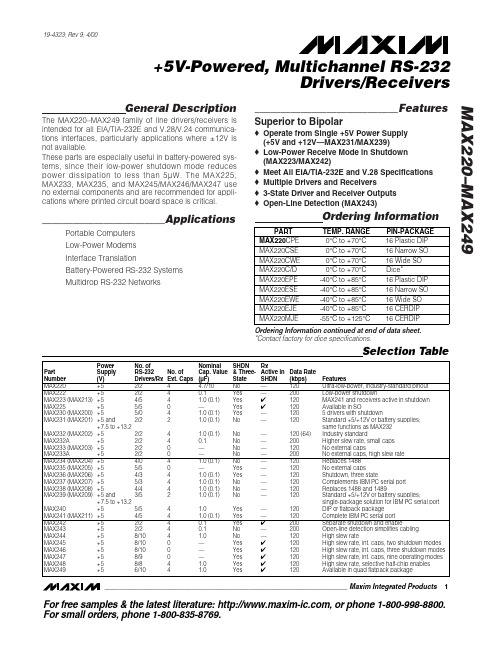
General DescriptionThe MAX220–MAX249 family of line drivers/receivers is intended for all EIA/TIA-232E and V.28/V.24 communica-tions interfaces, particularly applications where ±12V is not available.These parts are especially useful in battery-powered sys-tems, since their low-power shutdown mode reduces power dissipation to less than 5µW. The MAX225,MAX233, MAX235, and MAX245/MAX246/MAX247 use no external components and are recommended for appli-cations where printed circuit board space is critical.________________________ApplicationsPortable Computers Low-Power Modems Interface TranslationBattery-Powered RS-232 Systems Multidrop RS-232 Networks____________________________Features Superior to Bipolaro Operate from Single +5V Power Supply (+5V and +12V—MAX231/MAX239)o Low-Power Receive Mode in Shutdown (MAX223/MAX242)o Meet All EIA/TIA-232E and V.28 Specifications o Multiple Drivers and Receiverso 3-State Driver and Receiver Outputs o Open-Line Detection (MAX243)Ordering InformationOrdering Information continued at end of data sheet.*Contact factory for dice specifications.MAX220–MAX249+5V-Powered, Multichannel RS-232Drivers/Receivers________________________________________________________________Maxim Integrated Products 1Selection Table19-4323; Rev 9; 4/00Power No. of NominalSHDN RxPart Supply RS-232No. of Cap. Value & Three-Active in Data Rate Number (V)Drivers/Rx Ext. Caps (µF)State SHDN (kbps)FeaturesMAX220+52/24 4.7/10No —120Ultra-low-power, industry-standard pinout MAX222+52/2 4 0.1Yes —200Low-power shutdownMAX223 (MAX213)+54/54 1.0 (0.1)Yes ✔120MAX241 and receivers active in shutdown MAX225+55/50—Yes ✔120Available in SOMAX230 (MAX200)+55/04 1.0 (0.1)Yes —120 5 drivers with shutdownMAX231 (MAX201)+5 and2/2 2 1.0 (0.1)No —120Standard +5/+12V or battery supplies; +7.5 to +13.2same functions as MAX232MAX232 (MAX202)+52/24 1.0 (0.1)No —120 (64)Industry standardMAX232A+52/240.1No —200Higher slew rate, small caps MAX233 (MAX203)+52/20— No —120No external capsMAX233A+52/20—No —200No external caps, high slew rate MAX234 (MAX204)+54/04 1.0 (0.1)No —120Replaces 1488MAX235 (MAX205)+55/50—Yes —120No external capsMAX236 (MAX206)+54/34 1.0 (0.1)Yes —120Shutdown, three stateMAX237 (MAX207)+55/34 1.0 (0.1)No —120Complements IBM PC serial port MAX238 (MAX208)+54/44 1.0 (0.1)No —120Replaces 1488 and 1489MAX239 (MAX209)+5 and3/52 1.0 (0.1)No —120Standard +5/+12V or battery supplies;+7.5 to +13.2single-package solution for IBM PC serial port MAX240+55/54 1.0Yes —120DIP or flatpack package MAX241 (MAX211)+54/54 1.0 (0.1)Yes —120Complete IBM PC serial port MAX242+52/240.1Yes ✔200Separate shutdown and enableMAX243+52/240.1No —200Open-line detection simplifies cabling MAX244+58/104 1.0No —120High slew rateMAX245+58/100—Yes ✔120High slew rate, int. caps, two shutdown modes MAX246+58/100—Yes ✔120High slew rate, int. caps, three shutdown modes MAX247+58/90—Yes ✔120High slew rate, int. caps, nine operating modes MAX248+58/84 1.0Yes ✔120High slew rate, selective half-chip enables MAX249+56/1041.0Yes✔120Available in quad flatpack packageFor free samples & the latest literature: , or phone 1-800-998-8800.For small orders, phone 1-800-835-8769.M A X 220–M A X 249+5V-Powered, Multichannel RS-232Drivers/ReceiversABSOLUTE MAXIMUM RATINGS—MAX220/222/232A/233A/242/243ELECTRICAL CHARACTERISTICS—MAX220/222/232A/233A/242/243(V CC = +5V ±10%, C1–C4 = 0.1µF‚ MAX220, C1 = 0.047µF, C2–C4 = 0.33µF, T A = T MIN to T MAX ‚ unless otherwise noted.)Note 1:Input voltage measured with T OUT in high-impedance state, SHDN or V CC = 0V.Note 2:For the MAX220, V+ and V- can have a maximum magnitude of 7V, but their absolute difference cannot exceed 13V.Stresses beyond those listed under “Absolute Maximum Ratings” may cause permanent damage to the device. These are stress ratings only, and functional operation of the device at these or any other conditions beyond those indicated in the operational sections of the specifications is not implied. Exposure to absolute maximum rating conditions for extended periods may affect device reliability.Supply Voltage (V CC )...............................................-0.3V to +6V Input VoltagesT IN ..............................................................-0.3V to (V CC - 0.3V)R IN (Except MAX220)........................................................±30V R IN (MAX220).....................................................................±25V T OUT (Except MAX220) (Note 1).......................................±15V T OUT (MAX220)...............................................................±13.2V Output VoltagesT OUT ...................................................................................±15V R OUT .........................................................-0.3V to (V CC + 0.3V)Driver/Receiver Output Short Circuited to GND.........Continuous Continuous Power Dissipation (T A = +70°C)16-Pin Plastic DIP (derate 10.53mW/°C above +70°C)....842mW 18-Pin Plastic DIP (derate 11.11mW/°C above +70°C)....889mW20-Pin Plastic DIP (derate 8.00mW/°C above +70°C)..440mW 16-Pin Narrow SO (derate 8.70mW/°C above +70°C)...696mW 16-Pin Wide SO (derate 9.52mW/°C above +70°C)......762mW 18-Pin Wide SO (derate 9.52mW/°C above +70°C)......762mW 20-Pin Wide SO (derate 10.00mW/°C above +70°C)....800mW 20-Pin SSOP (derate 8.00mW/°C above +70°C)..........640mW 16-Pin CERDIP (derate 10.00mW/°C above +70°C).....800mW 18-Pin CERDIP (derate 10.53mW/°C above +70°C).....842mW Operating Temperature RangesMAX2_ _AC_ _, MAX2_ _C_ _.............................0°C to +70°C MAX2_ _AE_ _, MAX2_ _E_ _..........................-40°C to +85°C MAX2_ _AM_ _, MAX2_ _M_ _.......................-55°C to +125°C Storage Temperature Range.............................-65°C to +160°C Lead Temperature (soldering, 10sec).............................+300°CMAX220–MAX249+5V-Powered, Multichannel RS-232Drivers/Receivers_______________________________________________________________________________________3Note 3:MAX243 R2OUT is guaranteed to be low when R2IN is ≥0V or is floating.ELECTRICAL CHARACTERISTICS—MAX220/222/232A/233A/242/243 (continued)(V= +5V ±10%, C1–C4 = 0.1µF‚ MAX220, C1 = 0.047µF, C2–C4 = 0.33µF, T = T to T ‚ unless otherwise noted.)M A X 220–M A X 249+5V-Powered, Multichannel RS-232Drivers/Receivers 4_________________________________________________________________________________________________________________________________Typical Operating CharacteristicsMAX220/MAX222/MAX232A/MAX233A/MAX242/MAX243108-1051525OUTPUT VOLTAGE vs. LOAD CURRENT-4-6-8-2642LOAD CURRENT (mA)O U T P U T V O L T A G E (V )1002011104104060AVAILABLE OUTPUT CURRENTvs. DATA RATE65798DATA RATE (kbits/sec)O U T P U T C U R R E N T (m A )203050+10V-10VMAX222/MAX242ON-TIME EXITING SHUTDOWN+5V +5V 0V0V 500µs/div V +, V - V O L T A G E (V )MAX220–MAX249+5V-Powered, Multichannel RS-232Drivers/Receivers_______________________________________________________________________________________5V CC ...........................................................................-0.3V to +6V V+................................................................(V CC - 0.3V) to +14V V-............................................................................+0.3V to -14V Input VoltagesT IN ............................................................-0.3V to (V CC + 0.3V)R IN ......................................................................................±30V Output VoltagesT OUT ...................................................(V+ + 0.3V) to (V- - 0.3V)R OUT .........................................................-0.3V to (V CC + 0.3V)Short-Circuit Duration, T OUT ......................................Continuous Continuous Power Dissipation (T A = +70°C)14-Pin Plastic DIP (derate 10.00mW/°C above +70°C)....800mW 16-Pin Plastic DIP (derate 10.53mW/°C above +70°C)....842mW 20-Pin Plastic DIP (derate 11.11mW/°C above +70°C)....889mW 24-Pin Narrow Plastic DIP(derate 13.33mW/°C above +70°C)..........1.07W24-Pin Plastic DIP (derate 9.09mW/°C above +70°C)......500mW 16-Pin Wide SO (derate 9.52mW/°C above +70°C).........762mW20-Pin Wide SO (derate 10 00mW/°C above +70°C).......800mW 24-Pin Wide SO (derate 11.76mW/°C above +70°C).......941mW 28-Pin Wide SO (derate 12.50mW/°C above +70°C) .............1W 44-Pin Plastic FP (derate 11.11mW/°C above +70°C).....889mW 14-Pin CERDIP (derate 9.09mW/°C above +70°C)..........727mW 16-Pin CERDIP (derate 10.00mW/°C above +70°C)........800mW 20-Pin CERDIP (derate 11.11mW/°C above +70°C)........889mW 24-Pin Narrow CERDIP(derate 12.50mW/°C above +70°C)..............1W24-Pin Sidebraze (derate 20.0mW/°C above +70°C)..........1.6W 28-Pin SSOP (derate 9.52mW/°C above +70°C).............762mW Operating Temperature RangesMAX2 _ _ C _ _......................................................0°C to +70°C MAX2 _ _ E _ _...................................................-40°C to +85°C MAX2 _ _ M _ _ ...............................................-55°C to +125°C Storage Temperature Range.............................-65°C to +160°C Lead Temperature (soldering, 10sec).............................+300°CABSOLUTE MAXIMUM RATINGS—MAX223/MAX230–MAX241ELECTRICAL CHARACTERISTICS—MAX223/MAX230–MAX241(MAX223/230/232/234/236/237/238/240/241, V CC = +5V ±10; MAX233/MAX235, V CC = 5V ±5%‚ C1–C4 = 1.0µF; MAX231/MAX239,V CC = 5V ±10%; V+ = 7.5V to 13.2V; T A = T MIN to T MAX ; unless otherwise noted.)Stresses beyond those listed under “Absolute Maximum Ratings” may cause permanent damage to the device. These are stress ratings only, and functional operation of the device at these or any other conditions beyond those indicated in the operational sections of the specifications is not implied. Exposure to absolute maximum rating conditions for extended periods may affect device reliability.M A X 220–M A X 249+5V-Powered, Multichannel RS-232Drivers/Receivers 6_______________________________________________________________________________________ELECTRICAL CHARACTERISTICS—MAX223/MAX230–MAX241 (continued)(MAX223/230/232/234/236/237/238/240/241, V CC = +5V ±10; MAX233/MAX235, V CC = 5V ±5%‚ C1–C4 = 1.0µF; MAX231/MAX239,V CC = 5V ±10%; V+ = 7.5V to 13.2V; T A = T MIN to T MAX ; unless otherwise noted.)MAX220–MAX249+5V-Powered, Multichannel RS-232Drivers/Receivers_______________________________________________________________________________________78.56.54.55.5TRANSMITTER OUTPUT VOLTAGE (V OH ) vs. V CC7.08.0V CC (V)V O H (V )5.07.57.46.02500TRANSMITTER OUTPUT VOLTAGE (V OH )vs. LOAD CAPACITANCE AT DIFFERENT DATA RATES6.46.27.27.0LOAD CAPACITANCE (pF)V O H (V )1500100050020006.86.612.04.02500TRANSMITTER SLEW RATE vs. LOAD CAPACITANCE6.05.011.09.010.0LOAD CAPACITANCE (pF)S L E W R A T E (V /µs )1500100050020008.07.0-6.0-9.04.55.5TRANSMITTER OUTPUT VOLTAGE (V OL ) vs. V CC-8.0-8.5-6.5-7.0V CC (V)V O L (V )5.0-7.5-6.0-7.62500TRANSMITTER OUTPUT VOLTAGE (V OL )vs. LOAD CAPACITANCE AT DIFFERENT DATA RATES-7.0-7.2-7.4-6.2-6.4LOAD CAPACITANCE (pF)V O L (V )150010005002000-6.6-6.810-105101520253035404550TRANSMITTER OUTPUT VOLTAGE (V+, V-)vs. LOAD CURRENT-2-6-4-886CURRENT (mA)V +, V - (V )420__________________________________________Typical Operating CharacteristicsMAX223/MAX230–MAX241*SHUTDOWN POLARITY IS REVERSED FOR NON MAX241 PARTSV+, V- WHEN EXITING SHUTDOWN(1µF CAPACITORS)MAX220-13SHDN*V-O V+500ms/divM A X 220–M A X 249+5V-Powered, Multichannel RS-232Drivers/Receivers 8_______________________________________________________________________________________ABSOLUTE MAXIMUM RATINGS—MAX225/MAX244–MAX249ELECTRICAL CHARACTERISTICS—MAX225/MAX244–MAX249(MAX225, V CC = 5.0V ±5%; MAX244–MAX249, V CC = +5.0V ±10%, external capacitors C1–C4 = 1µF; T A = T MIN to T MAX ; unless oth-erwise noted.)Note 4:Input voltage measured with transmitter output in a high-impedance state, shutdown, or V CC = 0V.Stresses beyond those listed under “Absolute Maximum Ratings” may cause permanent damage to the device. These are stress ratings only, and functional operation of the device at these or any other conditions beyond those indicated in the operational sections of the specifications is not implied. Exposure to absolute maximum rating conditions for extended periods may affect device reliability.Supply Voltage (V CC )...............................................-0.3V to +6V Input VoltagesT IN ‚ ENA , ENB , ENR , ENT , ENRA ,ENRB , ENTA , ENTB ..................................-0.3V to (V CC + 0.3V)R IN .....................................................................................±25V T OUT (Note 3).....................................................................±15V R OUT ........................................................-0.3V to (V CC + 0.3V)Short Circuit (one output at a time)T OUT to GND............................................................Continuous R OUT to GND............................................................ContinuousContinuous Power Dissipation (T A = +70°C)28-Pin Wide SO (derate 12.50mW/°C above +70°C).............1W 40-Pin Plastic DIP (derate 11.11mW/°C above +70°C)...611mW 44-Pin PLCC (derate 13.33mW/°C above +70°C)...........1.07W Operating Temperature RangesMAX225C_ _, MAX24_C_ _ ..................................0°C to +70°C MAX225E_ _, MAX24_E_ _ ...............................-40°C to +85°C Storage Temperature Range.............................-65°C to +160°C Lead Temperature (soldering,10sec)..............................+300°CMAX220–MAX249+5V-Powered, Multichannel RS-232Drivers/Receivers_______________________________________________________________________________________9Note 5:The 300Ωminimum specification complies with EIA/TIA-232E, but the actual resistance when in shutdown mode or V CC =0V is 10M Ωas is implied by the leakage specification.ELECTRICAL CHARACTERISTICS—MAX225/MAX244–MAX249 (continued)(MAX225, V CC = 5.0V ±5%; MAX244–MAX249, V CC = +5.0V ±10%, external capacitors C1–C4 = 1µF; T A = T MIN to T MAX ; unless oth-erwise noted.)M A X 220–M A X 249+5V-Powered, Multichannel RS-232Drivers/Receivers 10________________________________________________________________________________________________________________________________Typical Operating CharacteristicsMAX225/MAX244–MAX24918212345TRANSMITTER SLEW RATE vs. LOAD CAPACITANCE86416LOAD CAPACITANCE (nF)T R A N S M I T T E R S L E W R A T E (V /µs )14121010-105101520253035OUTPUT VOLTAGEvs. LOAD CURRENT FOR V+ AND V--2-4-6-88LOAD CURRENT (mA)O U T P U T V O L T A G E (V )64209.05.012345TRANSMITTER OUTPUT VOLTAGE (V+, V-)vs. LOAD CAPACITANCE AT DIFFERENT DATA RATES6.05.58.5LOAD CAPACITANCE (nF)V +, V (V )8.07.57.06.5MAX220–MAX249Drivers/Receivers______________________________________________________________________________________11Figure 1. Transmitter Propagation-Delay Timing Figure 2. Receiver Propagation-Delay TimingFigure 3. Receiver-Output Enable and Disable Timing Figure 4. Transmitter-Output Disable TimingM A X 220–M A X 249Drivers/Receivers 12______________________________________________________________________________________ENT ENR OPERATION STATUS TRANSMITTERSRECEIVERS00Normal Operation All Active All Active 01Normal Operation All Active All 3-State10Shutdown All 3-State All Low-Power Receive Mode 11ShutdownAll 3-StateAll 3-StateTable 1a. MAX245 Control Pin ConfigurationsENT ENR OPERATION STATUS TRANSMITTERS RECEIVERSTA1–TA4TB1–TB4RA1–RA5RB1–RB500Normal Operation All Active All Active All Active All Active 01Normal Operation All Active All Active RA1–RA4 3-State,RA5 Active RB1–RB4 3-State,RB5 Active 1ShutdownAll 3-StateAll 3-StateAll Low-Power Receive Mode All Low-Power Receive Mode 11Shutdown All 3-State All 3-StateRA1–RA4 3-State,RA5 Low-Power Receive ModeRB1–RB4 3-State,RB5 Low-Power Receive ModeTable 1b. MAX245 Control Pin ConfigurationsTable 1c. MAX246 Control Pin ConfigurationsENA ENB OPERATION STATUS TRANSMITTERS RECEIVERSTA1–TA4TB1–TB4RA1–RA5RB1–RB500Normal Operation All Active All Active All Active All Active 01Normal Operation All Active All 3-State All Active RB1–RB4 3-State,RB5 Active 1ShutdownAll 3-StateAll ActiveRA1–RA4 3-State,RA5 Active All Active 11Shutdown All 3-State All 3-StateRA1–RA4 3-State,RA5 Low-Power Receive ModeRB1–RB4 3-State,RA5 Low-Power Receive ModeMAX220–MAX249Drivers/Receivers______________________________________________________________________________________13Table 1d. MAX247/MAX248/MAX249 Control Pin ConfigurationsM A X 220–M A X 249_______________Detailed DescriptionThe MAX220–MAX249 contain four sections: dual charge-pump DC-DC voltage converters, RS-232 dri-vers, RS-232 receivers, and receiver and transmitter enable control inputs.Dual Charge-Pump Voltage ConverterThe MAX220–MAX249 have two internal charge-pumps that convert +5V to ±10V (unloaded) for RS-232 driver operation. The first converter uses capacitor C1 to dou-ble the +5V input to +10V on C3 at the V+ output. The second converter uses capacitor C2 to invert +10V to -10V on C4 at the V- output.A small amount of power may be drawn from the +10V (V+) and -10V (V-) outputs to power external circuitry (see the Typical Operating Characteristics section),except on the MAX225 and MAX245–MAX247, where these pins are not available. V+ and V- are not regulated,so the output voltage drops with increasing load current.Do not load V+ and V- to a point that violates the mini-mum ±5V EIA/TIA-232E driver output voltage when sourcing current from V+ and V- to external circuitry. When using the shutdown feature in the MAX222,MAX225, MAX230, MAX235, MAX236, MAX240,MAX241, and MAX245–MAX249, avoid using V+ and V-to power external circuitry. When these parts are shut down, V- falls to 0V, and V+ falls to +5V. For applica-tions where a +10V external supply is applied to the V+pin (instead of using the internal charge pump to gen-erate +10V), the C1 capacitor must not be installed and the SHDN pin must be tied to V CC . This is because V+is internally connected to V CC in shutdown mode.RS-232 DriversThe typical driver output voltage swing is ±8V when loaded with a nominal 5k ΩRS-232 receiver and V CC =+5V. Output swing is guaranteed to meet the EIA/TIA-232E and V.28 specification, which calls for ±5V mini-mum driver output levels under worst-case conditions.These include a minimum 3k Ωload, V CC = +4.5V, and maximum operating temperature. Unloaded driver out-put voltage ranges from (V+ -1.3V) to (V- +0.5V). Input thresholds are both TTL and CMOS compatible.The inputs of unused drivers can be left unconnected since 400k Ωinput pull-up resistors to V CC are built in (except for the MAX220). The pull-up resistors force the outputs of unused drivers low because all drivers invert.The internal input pull-up resistors typically source 12µA,except in shutdown mode where the pull-ups are dis-abled. Driver outputs turn off and enter a high-imped-ance state—where leakage current is typically microamperes (maximum 25µA)—when in shutdownmode, in three-state mode, or when device power is removed. Outputs can be driven to ±15V. The power-supply current typically drops to 8µA in shutdown mode.The MAX220 does not have pull-up resistors to force the ouputs of the unused drivers low. Connect unused inputs to GND or V CC .The MAX239 has a receiver three-state control line, and the MAX223, MAX225, MAX235, MAX236, MAX240,and MAX241 have both a receiver three-state control line and a low-power shutdown control. Table 2 shows the effects of the shutdown control and receiver three-state control on the receiver outputs.The receiver TTL/CMOS outputs are in a high-imped-ance, three-state mode whenever the three-state enable line is high (for the MAX225/MAX235/MAX236/MAX239–MAX241), and are also high-impedance whenever the shutdown control line is high.When in low-power shutdown mode, the driver outputs are turned off and their leakage current is less than 1µA with the driver output pulled to ground. The driver output leakage remains less than 1µA, even if the transmitter output is backdriven between 0V and (V CC + 6V). Below -0.5V, the transmitter is diode clamped to ground with 1k Ωseries impedance. The transmitter is also zener clamped to approximately V CC + 6V, with a series impedance of 1k Ω.The driver output slew rate is limited to less than 30V/µs as required by the EIA/TIA-232E and V.28 specifica-tions. Typical slew rates are 24V/µs unloaded and 10V/µs loaded with 3Ωand 2500pF.RS-232 ReceiversEIA/TIA-232E and V.28 specifications define a voltage level greater than 3V as a logic 0, so all receivers invert.Input thresholds are set at 0.8V and 2.4V, so receivers respond to TTL level inputs as well as EIA/TIA-232E and V.28 levels.The receiver inputs withstand an input overvoltage up to ±25V and provide input terminating resistors withDrivers/Receivers 14Table 2. Three-State Control of ReceiversMAX220–MAX249Drivers/Receivers______________________________________________________________________________________15nominal 5k Ωvalues. The receivers implement Type 1interpretation of the fault conditions of V.28 and EIA/TIA-232E.The receiver input hysteresis is typically 0.5V with a guaranteed minimum of 0.2V. This produces clear out-put transitions with slow-moving input signals, even with moderate amounts of noise and ringing. The receiver propagation delay is typically 600ns and is independent of input swing direction.Low-Power Receive ModeThe low-power receive-mode feature of the MAX223,MAX242, and MAX245–MAX249 puts the IC into shut-down mode but still allows it to receive information. This is important for applications where systems are periodi-cally awakened to look for activity. Using low-power receive mode, the system can still receive a signal that will activate it on command and prepare it for communi-cation at faster data rates. This operation conserves system power.Negative Threshold—MAX243The MAX243 is pin compatible with the MAX232A, differ-ing only in that RS-232 cable fault protection is removed on one of the two receiver inputs. This means that control lines such as CTS and RTS can either be driven or left floating without interrupting communication. Different cables are not needed to interface with different pieces of equipment.The input threshold of the receiver without cable fault protection is -0.8V rather than +1.4V. Its output goes positive only if the input is connected to a control line that is actively driven negative. If not driven, it defaults to the 0 or “OK to send” state. Normally‚ the MAX243’s other receiver (+1.4V threshold) is used for the data line (TD or RD)‚ while the negative threshold receiver is con-nected to the control line (DTR‚ DTS‚ CTS‚ RTS, etc.). Other members of the RS-232 family implement the optional cable fault protection as specified by EIA/TIA-232E specifications. This means a receiver output goes high whenever its input is driven negative‚ left floating‚or shorted to ground. The high output tells the serial communications IC to stop sending data. To avoid this‚the control lines must either be driven or connected with jumpers to an appropriate positive voltage level.Shutdown—MAX222–MAX242On the MAX222‚ MAX235‚ MAX236‚ MAX240‚ and MAX241‚ all receivers are disabled during shutdown.On the MAX223 and MAX242‚ two receivers continue to operate in a reduced power mode when the chip is in shutdown. Under these conditions‚ the propagation delay increases to about 2.5µs for a high-to-low input transition. When in shutdown, the receiver acts as a CMOS inverter with no hysteresis. The MAX223 and MAX242 also have a receiver output enable input (EN for the MAX242 and EN for the MAX223) that allows receiver output control independent of SHDN (SHDN for MAX241). With all other devices‚ SHDN (SH DN for MAX241) also disables the receiver outputs.The MAX225 provides five transmitters and five receivers‚ while the MAX245 provides ten receivers and eight transmitters. Both devices have separate receiver and transmitter-enable controls. The charge pumps turn off and the devices shut down when a logic high is applied to the ENT input. In this state, the supply cur-rent drops to less than 25µA and the receivers continue to operate in a low-power receive mode. Driver outputs enter a high-impedance state (three-state mode). On the MAX225‚ all five receivers are controlled by the ENR input. On the MAX245‚ eight of the receiver out-puts are controlled by the ENR input‚ while the remain-ing two receivers (RA5 and RB5) are always active.RA1–RA4 and RB1–RB4 are put in a three-state mode when ENR is a logic high.Receiver and Transmitter EnableControl InputsThe MAX225 and MAX245–MAX249 feature transmitter and receiver enable controls.The receivers have three modes of operation: full-speed receive (normal active)‚ three-state (disabled)‚ and low-power receive (enabled receivers continue to function at lower data rates). The receiver enable inputs control the full-speed receive and three-state modes. The transmitters have two modes of operation: full-speed transmit (normal active) and three-state (disabled). The transmitter enable inputs also control the shutdown mode. The device enters shutdown mode when all transmitters are disabled. Enabled receivers function in the low-power receive mode when in shutdown.M A X 220–M A X 249Tables 1a–1d define the control states. The MAX244has no control pins and is not included in these tables. The MAX246 has ten receivers and eight drivers with two control pins, each controlling one side of the device. A logic high at the A-side control input (ENA )causes the four A-side receivers and drivers to go into a three-state mode. Similarly, the B-side control input (ENB ) causes the four B-side drivers and receivers to go into a three-state mode. As in the MAX245, one A-side and one B-side receiver (RA5 and RB5) remain active at all times. The entire device is put into shut-down mode when both the A and B sides are disabled (ENA = ENB = +5V).The MAX247 provides nine receivers and eight drivers with four control pins. The ENRA and ENRB receiver enable inputs each control four receiver outputs. The ENTA and ENTB transmitter enable inputs each control four drivers. The ninth receiver (RB5) is always active.The device enters shutdown mode with a logic high on both ENTA and ENTB .The MAX248 provides eight receivers and eight drivers with four control pins. The ENRA and ENRB receiver enable inputs each control four receiver outputs. The ENTA and ENTB transmitter enable inputs control four drivers each. This part does not have an always-active receiver. The device enters shutdown mode and trans-mitters go into a three-state mode with a logic high on both ENTA and ENTB .The MAX249 provides ten receivers and six drivers with four control pins. The ENRA and ENRB receiver enable inputs each control five receiver outputs. The ENTA and ENTB transmitter enable inputs control three dri-vers each. There is no always-active receiver. The device enters shutdown mode and transmitters go into a three-state mode with a logic high on both ENTA and ENTB . In shutdown mode, active receivers operate in a low-power receive mode at data rates up to 20kbits/sec.__________Applications InformationFigures 5 through 25 show pin configurations and typi-cal operating circuits. In applications that are sensitive to power-supply noise, V CC should be decoupled to ground with a capacitor of the same value as C1 and C2 connected as close as possible to the device.Drivers/Receivers16______________________________________________________________________________________。

General DescriptionThe MAX6326/MAX6327/MAX6328/MAX6346/MAX6347/MAX6348 microprocessor (µP) supervisory circuits moni-tor the power supplies in µP and digital systems. These devices provide excellent circuit reliability and low cost by eliminating external components and adjustments when used with 2.5V, 3V, 3.3V, and 5V powered circuits.These circuits perform a single function: they assert a reset signal whenever the V CC supply voltage declines below a preset threshold, keeping it asserted for at least 100ms after V CC has risen above the reset threshold.The only difference between the devices is their output.The MAX6326/MAX6346 (push-pull) and MAX6328/MAX6348 (open-drain) have an active-low reset output.The MAX6327/MAX6347 have an active-high push-pull reset output. All of these parts are guaranteed to be in the correct state for V CC down to 1V. The reset compara-tor is designed to ignore fast transients on V CC . Reset thresholds are factory-trimmable between 2.2V and 4.63V, in approximately 100mV increments. Twenty-one standard versions are available. Contact the factory for availability of nonstandard versions.Ultra-low supply currents (1µA max for the MAX6326/MAX6327/MAX6328) make these parts ideal for use in portable equipment. All six devices are available in space-saving SOT23 and SC70 packages.ApplicationsComputers Intelligent Instruments Controllers AutomotiveCritical µP and µC Portable/Battery-Powered Power MonitoringEquipmentFeatures♦Ultra-Low 1µA (max) Supply Current (MAX6326/MAX6327/MAX6328)♦Precision Monitoring of 2.5V, 3V, 3.3V, and 5V Power-Supply Voltages♦Reset Thresholds Available from 2.2V to 4.63V ♦Fully Specified Over Temperature♦100ms (min) Power-On Reset Pulse Width ♦Low Cost♦Available in Three Versions: Push-Pull RESET ,Push-Pull RESET, and Open-Drain RESET ♦Power-Supply Transient Immunity ♦No External Components ♦3-Pin SC70/SOT23 Packages♦Pin Compatible with MAX803/MAX809/MAX810MAX6326/MAX6327/MAX6328/MAX6346/MAX6347/MAX63483-Pin, Ultra-Low-Power SC70/SOTµP Reset Circuits________________________________________________________________Maxim Integrated Products 1Pin Configuration19-1294; Rev 4; 12/05†The MAX6326/MAX6327/MAX6328/MAX6346/MAX6347/MAX6348 are available in factory-set V CC reset thresholds from 2.2V to 4.63V, in approximately 0.1V increments. Choose the desired reset-threshold suffix from Table 1 and insert it in the blank spaces following “R.”There are 21 standard versions with a required order increment of 2500 pieces. Sample stock is gen-erally held on the standard versions only (see the SelectorGuide). Required order increment is 10,000 pieces for nonstan-dard versions (Table 2). Contact factory for availability. All devices available in tape-and-reel only.Devices are available in both leaded and lead-free packaging.Specify lead-free by replacing “-T” with “+T” when ordering.Selector Guide appears at end of data sheet.For pricing, delivery, and ordering information,please contact Maxim/Dallas Direct!at 1-888-629-4642, or visit Maxim’s website at .M A X 6326/M A X 6327/M A X 6328/M A X 6346/M A X 6347/M A X 63483-Pin, Ultra-Low-Power SC70/SOT µP Reset Circuits 2_______________________________________________________________________________________ABSOLUTE MAXIMUM RATINGSELECTRICAL CHARACTERISTICS(V CC = full range, T A = -40°C to +85°C, unless otherwise noted. Typical values are at T A = +25°C and V CC = 3V.) (Note 1)Stresses beyond those listed under “Absolute Maximum Ratings” may cause permanent damage to the device. These are stress ratings only, and functional operation of the device at these or any other conditions beyond those indicated in the operational sections of the specifications is not implied. Exposure to absolute maximum rating conditions for extended periods may affect device reliability.Terminal Voltage (with respect to GND)V CC ...........................................................................-0.3V to +6V RESET, RESET (push-pull).........................-0.3V to (V CC + 0.3V)RESET (open drain)..................................................-0.3V to +6V Input Current (V CC ).............................................................20mA Output Current (RESET, RESET ).........................................20mA Rate of Rise (V CC )...........................................................100V/µsContinuous Power Dissipation (T A = +70°C)3-Pin SC70 (derate 2.7mW/°C above +70°C)...............174mW 3-Pin SOT23 (derate 4mW/°C above +70°C)................320mW Operating Temperature Range ...........................-40°C to +85°C Storage Temperature Range.............................-65°C to +150°C Lead Temperature (soldering, 10s).................................+300°CNote 1:Overtemperature limits are guaranteed by design and not production tested.MAX6326/MAX6327/MAX6328/MAX6346/MAX6347/MAX63483-Pin, Ultra-Low-Power SC70/SOTµP Reset Circuits_______________________________________________________________________________________3__________________________________________Typical Operating Characteristics(T A = +25°C, unless otherwise noted.)00.30.20.10.40.50.60.70.80.91.0-400-2020406080SUPPLY CURRENT vs. TEMPERATURE TEMPERATURE (°C)S U P P L Y C U R R E N T(µA)050100150200-400-2020406080POWER-DOWN RESET DELAY vs. TEMPERATURE TEMPERATURE (°C)R E S E T D E L A Y(µs)130150140160170180190200210-400-2020406080POWER-UP RESET TIMEOUT vs. TEMPERATURE M A X6326-03TEMPERATURE (°C)P O W E R-U P R E S E T T I M E O U T(m s)500011001000MAXIMUM TRANSIENT DURATION vs. RESET THRESHOLD OVERDRIVE (SC70)100300400200M A X6326-04RESET THRESHOLD OVERDRIVE,V TH - V CC (mV)M A X I M U M T R A N S I E N T D U R A T I O N(µs)10______________________________________________________________Pin DescriptionM A X 6326/M A X 6327/M A X 6328/M A X 6346/M A X 6347/M A X 63483-Pin, Ultra-Low-Power SC70/SOT µP Reset Circuits 4___________________________________________________________________________________________________Applications InformationInterfacing to µPs with Bidirectional Reset PinsSince the RESET output on the MAX6328/MAX6348 is open drain, these devices interface easily with micro-processors (µPs) that have bidirectional reset pins,such as the Motorola 68HC11. Connecting the µP supervisor’s RESET output directly to the microcon-troller’s (µC’s) RESET pin with a single pull-up resistor allows either device to assert reset (Figure 1).Negative-Going V CC TransientsIn addition to issuing a reset to the µP during power-up,power-down, and brownout conditions, these devices are relatively immune to short-duration, negative-going V CC transients (glitches).The Typical O perating Characteristics show the Maxi-mum Transient Duration vs. Reset Threshold Overdrive graph, for which reset pulses are not generated. The graph shows the maximum pulse width that a negative-going V CC transient may typically have when issuing a reset signal. As the amplitude of the transient increas-es, the maximum allowable pulse width decreases.Figure 1. Interfacing to µPs with Bidirectional Reset PinsTable 1. Factory-Trimmed Reset Thresholds ‡‡Factory-trimmed reset thresholds are available in approximately 100mV increments with a 1.5% room-temperature variance.MAX6326/MAX6327/MAX6328/MAX6346/MAX6347/MAX63483-Pin, Ultra-Low-Power SC70/SOTµP Reset Circuits_______________________________________________________________________________________5Table 1. Factory-Trimmed Reset Thresholds‡(continued)‡Factory-trimmed reset thresholds are available in approximately 100mV increments with a 1.5% room-temperature variance.Table 2. Device Marking Codes and Minimum Order IncrementsM A X 6326/M A X 6327/M A X 6328/M A X 6346/M A X 6347/M A X 63483-Pin, Ultra-Low-Power SC70/SOT µP Reset Circuits 6__________________________________________________________________________________________________________Chip InformationTRANSISTOR COUNT: 419Table 2. Device Marking Codes and Minimum Order Increments (continued)Selector Guide(standard versions*)*Sample stock is generally held on all standard versions.Package Information MAX6326/MAX6327/MAX6328/MAX6346/MAX6347/MAX63483-Pin, Ultra-Low-Power SC70/SOTµP Reset Circuits_______________________________________________________________________________________ (The package drawing(s) in this data sheet may not reflect the most current specifications. For the latest package outline information,go to /packages.)7M A X 6326/M A X 6327/M A X 6328/M A X 6346/M A X 6347/M A X 63483-Pin, Ultra-Low-Power SC70/SOT µP Reset Circuits Maxim cannot assume responsibility for use of any circuitry other than circuitry entirely embodied in a Maxim product. No circuit patent licenses are implied. Maxim reserves the right to change the circuitry and specifications without notice at any time.8_____________________Maxim Integrated Products, 120 San Gabriel Drive, Sunnyvale, CA 94086 408-737-7600©2005 Maxim Integrated ProductsPrinted USAis a registered trademark of Maxim Integrated Products, Inc.Package Information (continued)(The package drawing(s) in this data sheet may not reflect the most current specifications. For the latest package outline information,go to /packages .)。