EMIF02-MIC03C2;中文规格书,Datasheet资料
- 格式:pdf
- 大小:304.11 KB
- 文档页数:8

MIC3003GFLFOM Management IC with Internal CalibrationMLF and MicroLead Frame are registered trademarks of Amkor Technology, Inc.General DescriptionThe MIC3003GFL is a fiber optic module controller which enables the implementation of sophisticated, hot-pluggable fiber optic transceivers with intelligent laser control and an internally calibrated Digital Diagnostic Monitoring Interface per SFF-8472. It essentially integrates all non-data path functions of an SFP/SFP+ transceiver into a tiny (3mm x 3mm ) MLF ® package. It also works well as a microcontroller peripheral in transponders or 10Gbps transceivers. The MIC3003GFL uses the same die as the MIC3003 with all its functions, but in a smaller package and different pin out. A highly configurable automatic power control (APC) circuit controls laser bias. Bias and modulation are temperature compensated using dual DACs, an on-chip temperature sensor, and NVRAM look-up tables. A programmable internal feedback resistor provides a wide dynamic range for the APC. Controlled laser turn-on.An analog-to-digital converter converts the measured temperature, voltage, bias current, transmit power, and received power from analog to digital. An EEPOT provides front-end adjustment of RX power. Each parameter is compared against user-programmed warning and alarm thresholds. Analog comparators and DACs provide fast monitoring of received power and critical laser operating parameters. Data can be reported as either internally calibrated or externally calibrated.An interrupt output, power-on hour meter, and data-ready bits add user friendliness beyond SFF-8472. The interrupt output and data-ready bits reduce overhead in the host system. The power-on hour meter logs operating hours using an internal real-time clock and stores the result in NVRAM.In addition to the features listed above, the MIC3003 features an extended temperature range, options to mask alarms and warnings interrupt and TXFAULT, a reset signal source, and the ability to support up to four chips with the same address on the serial interface. It also supports eight-byte SMBus block writes.Communication with the MIC3003 is via an industry standard 2-wire SMBus serial interface. Nonvolatile memory is provided for serial ID, configuration, and separate OEM and user scratchpad spaces.Datasheets and support documentation can be found on Micrel’s web site at: .Features• Packaged in a ultra small (3mm x 3mm) 24-pin MLF ® package • Extended temperature range• Alarms and warnings interrupt and TXFAULT masks • Capability to support up to four devices on one SMBus • APC or constant-current laser bias• Turbo mode for APC loop start-up and shorter laser turn on time • Supports multiple laser types and bias circuit topologies • Integrated digital temperature sensor• Temperature compensation of modulation, bias, bias fault and alarm thresholds via NVRAM look-up tables • NVRAM to support GBIC/SFP serial ID function • User writable EEPROM scratchpad• Reset signal compatible with some new systems requirements • Diagnostic monitoring interface per SFF-8472 – Monitors and reports critical parameters:temperature, bias current, TX and RX optical power, and supply voltage– S/W control and monitoring of TXFAULT, RXLOS, RATESELECT, and TXDISABLE – Internal or external calibration– EEPOT for adjusting RX power measurement • Power-on hour meter • Interrupt capability• Extensive test and calibration features • 2-wire SMBus-compatible serial interface • SFP/SFP+ MSA and SFF-8472 compliant • 3.0V to 3.6V power supply range • 5V-tolerant I/OApplications• SFP/SFP+ optical transceivers• SONET/SDH transceivers and transponders • Fibre Channel transceivers • 10Gbps transceivers• Free space optical communications • Proprietary optical linksTypical ApplicationOrdering InformationPart NumberPackage Marking Junction Temp.RangePackage Type Lead FinishMIC3003GFL GFL 3003 with Pb-Free bar-line indicator–45°C to +105°C24-pin (3mm x 3mm) MLF ® Pb-Free,NiPdAuMIC3003GFLTR (1) GFL 3003 with Pb-Free bar-line indicator–45°C to +105°C24-pin (3mm x 3mm) MLF ® Pb-Free,NiPdAuNote:1. Tape and Reel.ContentsGeneral Description (1)Features (1)Pin Configuration (8)Pin Configuration (8)Pin Description (MIC3003GFL only) (8)Absolute Maximum Ratings (10)Operating Ratings (10)Electrical Characteristics (10)Electrical Characteristics (12)Electrical Characteristics (13)Serial Interface Timing Diagram (14)Serial Interface Address Maps (15)Block Diagram (18)Analog-to-Digital Converter/Signal Monitoring (18)Alarms and Warnings Interrupt Source Masking (19)Alarms and Warnings as TXFAULT Source (21)Latching of Alarms and Warnings (21)SMBus Multipart Support (21)QGOP Pin Function (21)Calibration Modes (22)A/ External Calibration (22)Voltage (22)Temperature (22)Bias Current (22)TX Power (22)RX Power (23)B/ Internal Calibration (23)Computing Internal Calibration Results (23)C/ Reading the ADC Result Registers (25)RXPOT (25)Laser Diode Bias Control (25)Laser Modulation Control (26)Power On and Laser Start-Up (27)Fault Comparators (28)SHDN and TXFIN (29)Temperature Measurement (30)Diode Faults (30)Temperature Compensation (30)Alarms and Warning Flags (32)Control and Status I/O (32)System Timing (34)Warm Resets (36)Power-On Hour Meter (36)Test and Calibration Features (37)Serial Port Operation (38)Block Writes (38)Acknowledge Polling (39)Write Protection and Data Security (39)OEM Password (39)OEM Mode and User Mode (39)Detailed Register Descriptions (40)Alarm Threshold Registers (40)Temperature High Alarm Threshold (40)Temperature Low Alarm Threshold (40)Voltage High Alarm Threshold (40)D[7] read/write (40)Bias Current High Alarm Threshold (41)Bias Current Low Alarm Threshold (41)TX Optical Power High Alarm Threshold (41)TX Optical Power Low Alarm Threshold (42)RX Optical Power High Alarm Threshold (42)RX Optical Power Low Alarm Threshold (42)Warning Threshold Registers (43)Temperature High Warning Threshold (43)Temperature Low Warning Threshold (43)Voltage High Warning Threshold (43)Voltage Low Warning Threshold (44)Bias Current High Warning Threshold (44)Bias Current Low Warning Threshold (44)TX Optical Power High Warning (44)TX Optical Power Low Warning (45)RX Optical Power High Warning Threshold (45)RX Optical Power Low Warning Threshold (45)Checksum (CHKSUM) Checksum of bytes 0 - 94 at serial address A2h (45)ADC Result Registers (46)Temperature Result (46)Voltage (46)Laser Diode Bias Current (46)Transmitted Optical Power (47)Received Optical Power (47)Control and Status (CNTRL) (47)Application Select Control Mode (ASCM) (48)Alarm Flags (50)Alarm Status Register 0 (ALARM0) (50)Alarm Status Register 1 (ALARM1) (50)Warning Flags (51)Warning Status Register 0 (WARN0) (51)Warning Status Register 1 (WARN1) (51)Extended Control and Status (ECNTRL) (52)OEM Password Entry (OEMPW) (52)Power-On Hours (POHh and POHl) (53)Data Ready Flags (DATARDY) (53)User Control Register (USRCTL) (54)RESETOUT (54)OEM Configuration Register 0 (OEMCFG0) (55)OEM Configuration Register 1 (OEMCFG1) (56)OEM Configuration Register 2 (OEMCFG2) (57)APC Setpoint 0, 1, and 2 (APCSET0, APCSET1, APCSET2) Automatic Power Control Setpoint (58)Modulation Setpoint 0, 1, and 2 (MODSET0, MODSET1, and MODSET2) Nominal V MOD Setpoint (58)I BIAS Fault Threshold (IBFLT) Bias Current Fault Threshold (59)Transmit Power Fault Threshold (TXFLT) (59)Loss-Of-Signal Threshold (LOSFLT) (59)Fault Suppression Timer (FLTTMR) Fault Suppression Interval in Increments of 0.5 ms (60)Fault Mask (FLTMSK) (60)OEM Password Setting (OEMPWSET) (61)OEM Calibration 0 (OEMCAL0) (61)OEM Calibration 1 (OEMCAL1) (63)LUT Index (LUTINDX) (64)OEM Configuration 3 (OEMCFG3) (64)BIAS DAC Setting (APCDAC) Current VBIAS Setting (65)Modulation DAC Setting (MODDAC) Current VMOD Setting (66)OEM Readback Register (OEMRD) (66)OEM Configuration 4 (OEMCFG4) (67)OEM Configuration 5 (OEMCFG5) (68)OEM Configuration 6 (OEMCFG6) (69)Power-On Hour Meter Data (POHDATA) (70)OEM Scratchpad Registers (SCRATCHn) (71)RX Power Coefficient Look-up Table (RXLUTn) (71)Calibration Constants (CALCOEFn) (72)Manufacturer ID Register (MFG_ID) Identifies Micrel as the manufacturer of the device. Always returns 2Ah (72)Device ID Register (DEV_ID) (73)Package Information (74)Figure 1. MIC3003 Block Diagram (18)Figure 2. Analog-to-Digital Converter Block Diagram (18)Figure 3. Internal Calibration RX Power Linear Approximation (25)Figure 4. RXPOT Block Diagram (25)Figure 5. APC and Modulation Control Block Diagram (26)Figure 6. Programmable Feedback Resistor (26)Figure 7. Transmitter Configurations Supported by MIC3003 (26)Figure 8. V MOD Configured as Voltage Output with Gain (27)Figure 9. MIC3003 Power-On Timing (OE = 1) (28)Figure 10. Fault Comparator Logic (28)Figure 11. Saturation Detector (29)Figure 12. RXLOS Comparator Logic (29)Figure 14. Transmitter On-Off Timing (34)Figure 15. Initialization Timing with TXDISABLE Asserted (34)Figure 16. Initialization Timing with TXDISABLE Not Asserted (34)Figure 17. Loss-of-Signal (LOS) Timing (35)Figure 19. Successfully Clearing a Fault Condition (36)Figure 20. Unsuccessful Attempt to Clear a Fault (36)Figure 21. Write Byte Protocol (38)Figure 22. Read Byte Protocol (38)Figure 23. Read_Word Protocol (38)Figure 24. Eight-Byte Block Write Protocol (39)Table 1. Serial Interface Address Map, Device Address = A0h (15)Table 2. Serial Interface Address Map, Device Address = A2 (15)Table 3. Serial Interface Address Map (Temperature Compensation Tables), Device Address = A4h (16)Table 4. Serial Interface Address Map (OEM Configuration Registers), Device Address = A6h (17)Table 5. A/D Input Signal Ranges and Resolutions (19)Table 6. V AUX Input Signal Ranges and Resolutions (19)Table 7. Alarms Interrupt Sources Masking Bits (20)Table 8. Warnings Interrupt Sources Masking Bits (20)Table 9. RESETOUT Clear Delay (21)Table 10. LSB Values of Offset Coefficients (23)Table 11. Internal Calibration Coefficient Memory Map – Part I (24)Table 12. Internal Calibration Coefficient Memory Map – Part II (24)Table 13. Shutdown State of SHDN vs. Configuration Bits (27)Table 14. Shutdown State of V BIAS vs. Configuration Bits (27)Table 15. Shutdown State of V MOD vs. Configuration Bits (27)Table 16. Temperature Compensation Look-up Tables (30)Table 17. APC Temperature Compensation Look-Up Table (31)Table 18. I MOD Temperature Compensation Look-Up Table (31)Table 19. I BIAS Comparator Temperature Compensation Look-Up Table (31)Table 20. BIAS Current High Alarm Temperature Compensation Table (31)Table 21. MIC3003 Alarm and Warning Events (33)Table 22. Test and Diagnostic Features (37)Pin Configuration24-Pin MLF® (ML)Pin Description (MIC3003GFL only)Pin Number Pin Name Pin Function1 VDDD Power supply input for digital functions.Open-drain output. Can be selected (via OEMCFG3 bit 7) to be an open-drain GPO or an active-2 QGPOlow, open-drain, pulsed reset signal output controlled by the status of bits [0-2] of byte A2h: FFh.3 GNDD Ground return for digital functions.Digital input. Receiver Rate Select input. OR’ed with soft rate select bit SRS0 to determine the4 RS0state of the RRSOUT pin. The state of this pin is always reflected in the RS0S bit.If bit 4 (IE) in the USRCTL register is set to 0 (its default value), this pin is configured as an analog5 VIN/INTinput. If IE bit is set to 1, this pin is configured as an open-drain output.Analog input: Multiplexed A/D input for monitoring supply voltage, with a 0V to 5.5V input range.Open-drain output: outputs the internally generated active-low interrupt signal /INT.6 CLK Digital input. Serial clock input.7 DATA Digital I/O, open-drain, bi-directional serial data input/output.Digital input; Active high. The transmitter is disabled when this input is high or the STXDIS bit is8 TXDISABLEset to 1. The state of this input is always reflected in the TXDIS bit.Digital Output; Open-Drain, with programmable polarity. If OEMCFG5 bit 4 is set to 0, a high level9 TXFAULTindicates a hardware fault impeding transmitter operation. If OEMCFG5 bit 4 is set to 1, a low levelindicates a hardware fault impeding transmitter operation. The state of this pin is always reflectedin the TXFLT bit.Digital Input; Transmitter Rate Select Input; OR’ed with soft rate select bit SRS1 to determine the10 RS1state of the TRSOUT pin. The state of this pin is always reflected in the RS1S bit.Analog Input. Multiplexed A/D converter input for monitoring received optical power. The input11 VRXrange is 0 to V REF. A 5-bit programmable EEPOT on this pin provides coarse calibration andranging of the RX power measurement.Pin Number Pin Name Pin Function12 SHDN/TXFINDigital output/Input; programmable polarity. When used as shutdown output (SHDN), OEMCFG3bit 2 set to 0, SHDN is asserted at the detection of a fault condition if OEMCFG4 bit 7 is set to 0. IfOEMCFG4 bit 7 is set to 1, a fault condition will not assert SHDN. When programmed as TXFIN, itis an input for external fault signals to be OR’ed with the internal fault sources to drive TXFAULT.13 VILD+Analog Input. Multiplexed A/D input for monitoring laser bias current via a sense resistor (signalinput); accommodates inputs referenced to V DD or GND (see pin 14 description).14 VILD–Analog Input. Reference terminal for the multiplexed pseudo-differential A/D converter inputs formonitoring laser bias current via a sense resistor (VILD+ is the sensing input). Tie to V DD or GNDto reference the voltage sensed on VILD+ to V DD or GND, respectively.15 VDDA Power supply input for analog functions.16 GNDA Ground return for analog functions.17 VMPDAnalog Input. Multiplexed A/D converter input for monitoring transmitted optical power via amonitor photodiode. In most applications, VMPD will be connected directly to FB. The input rangeis 0 - V REF or 0 - V REF/4 depending upon the setting of the APC configuration bits18 FBAnalog Input. Feedback voltage for the APC loop op-amp. Polarity and scale are programmablevia the APC configuration bits I OEMCFG1. Connect to V BIAS if APC is not used.19 VMODAnalog Output. Buffered DAC output to set the modulation current on the laser driver IC. Operateswith either a 0– V REF or a (V DD–V REF) – V DD output swing so as to generate either a ground-referenced or a V DD referenced programmed voltage. A simple external circuit can be used togenerate a programmable current for those drivers that require a current rather than a voltageinput.20 VMOD–Analog input. This pin is the inverting terminal of the VMOD buffer op-amp. Connect to VMOD(gain = 1) or a feedback resistor network to set a different gain value.21 VBIASAnalog output. Buffered DAC output capable of sourcing or sinking up to 10mA under control ofthe APC function to drive an external transistor or the APCSET pin of a laser diode driver for laserdiode DC bias. The output and feedback polarity are programmable to accommodate either anNPN or a PNP transistor to drive a common-anode or common-cathode laser diode.22 COMPAnalog output. Compensation terminal for the APC loop. Connect a capacitor between this pin andGNDA or V DDA with the appropriate value to tune the APC loop time constant to a desirable value.23 RRSOUT/GPO Digital Output. Open-Drain or push-pull.If OEMCFG3 bit 4 is set to 0, RRSOUT is selected. It represents the receiver rate select as per SFF. This output is controlled by the SRS0 bit OR’ed with RS0 input and is open drain only.If OEMCFG3 bit 4 is set to 1, GPO is selected. General-purpose, non-volatile output, it is controlled by the GPO configuration bits in OEMCFG3.24 RXLOS/TRSOUT Digital output. This programmable polarity, open-drain outputs has two purposes:If OEMCFG6 bit 2 = 0, indicates the loss of the received signal as indicated by a level of received optical power below the programmed RXLOS comparator threshold; may be wire-OR’ed with external signals. Normal operation is indicated by a low level when OEMCFG6 bit 3 is set to 0 and a high level when OEMCFG6 bit 3 is set to 1. RXLOS is de-asserted when VRX > LOSFLTn. The LOS bit reflects the state of RXLOS whether driven by the MIC3003 or an external circuit.If OEMCFG6 bit 2 = 1, TRSOUT is selected. This signal represents the transmitter rate select as per the SFF specification. This output is controlled by the SRS1 bit OR’ed with the RS1 input.Absolute Maximum Ratings(1)Power Supply Voltage, V DD.......................................+3.8V Voltage on CLK, DATA, TXFAULT, VIN, RXLOS, TXDISABLE, RS0, RS1.........................–0.3V to +6.0V Voltage On Any Other Pin.....................–0.3V to V DD+0.3V Power Dissipation, T A = 85°C....................................1.5W Junction Temperature (T J).......................................150°C Storage Temperature (T S).......................–65°C to +150°C Soldering (20 sec.)...................................................260ºC ESD Ratings(3)Human Body Model..................................................2kV Machine Model.......................................................300V Operating Ratings(2)Power Supply Voltage, V DDA/V DDD...........+3.0V to +3.6V Ambient Temperature Range (T A) .......–40°C to +105°C Package Thermal ResistanceMLF® (θJA).................................................60°C/WElectrical CharacteristicsFor typical values, T A = 25°C, V DDA = V DDD = +3.3V, unless otherwise noted. Bold values are guaranteed for +3.0V ≤ (V DDA = V DDD)≤ 3.6V, T(min)≤ T A≤ T(min), (8)Symbol Parameter Condition Min Typ Max Units Power SupplyCLK = DATA = V DDD= V DDA; TXDISABLE low; all DACs at full-scale; all A/D inputs at full-scale; all other pins open. 2.3 3.5 mAI DD SupplyCurrentCLK = DATA = V DDD= V DDA; TXDISABLEhigh; FLTDAC at full-scale; all A/D inputsat full-scale; all other pins open.2.33.5 mAV POR Power-on Reset Voltage All registers reset to default values;A/D conversions initiated. 2.92.98 VVUVLOUnder-Voltage Lockout Threshold Note 5 2.5 2.73 VVHYSTPower-on Reset Hysteresis Voltage 170 mVtPORPower-on Reset Time V DD > V POR, Note 4 50 µs V REF ReferenceVoltage 1.2101.2251.240 V ΔV REF/ΔV DDAVoltage Reference Line Regulation 1.7 mV/V Temperature-to-Digital Converter CharacteristicsLocal Temperature MeasurementError–40°C ≤ T A≤ +105°C, Note 6 ±1 ±3 °Ct CONV Conversion Time Note 4 60 mst SAMPLE SamplePeriod 100 ms Voltage-to-Digital Converter Characteristics (V RX, V AUX, V BIAS, V MPD, V ILD±)Voltage Measurement Error –40°C ≤ T A≤ +105°C, Note 6 ±1 ±2.0 %fst CONV Conversion Time Note 4 10 mst SAMPLE Sample Period Note 4 100 ms Notes:1. Exceeding the absolute maximum rating may damage the device.2. The device is not guaranteed to function outside its operating rating.3. Devices are ESD sensitive. Handling precautions recommended. Human body model, 1.5k in series with 100pF.4. Guaranteed by design and/or testing of related parameters. Not 100% tested in production.5. The MIC3003 will attempt to enter its shutdown state when V DD falls below V UVLO. This operation requires time to complete. If the supply voltage fallstoo rapidly, the operation may not be completed.6. Does not include quantization error.分销商库存信息:MICRELMIC3003GFL MIC3003GFL TR。

Multi-contact, Labor-saving, Environment-friendly, Next-generation Safety-door Switch•Lineup includes three contact models with 2NC/1NO and 3NC contact forms and MBB models in addition to the previous contact forms 1NC/1NO, and 2NC.•M12-connector models are available, saving on labor and simplifying replacement.•Standardized gold-clad contacts provide high contact reliability.Applicable to both standard loads and micro -loads.•Variety of metallic heads available.•Conforms to ISO 14119.Model Number StructureModel Number LegendSwitch (Standard type)1.Conduit/Connector size 1:Pg13.5 (1-conduit)2:G1/2 (1-conduit)4:M20 (1-conduit)6:G1/2 (2-conduit)8:M20 (2-conduit)9:M12 connector (1-conduit)2.Built-in SwitchA:1NC/1NO (slow-action)B:2NC (slow-action)C:2NC/1NO (slow-action)D:3NC (slow-action)E:1NC/1NO (MBB contact)F:2NC/1NO (MBB contact)3.Head Mounting DirectionF:Four mounting directions possible (Front-side mounting atshipping)/plasticD:Four mounting directions possible (Front-side mounting atshipping)/metal Note:An order for the head part or the switch part alone cannot beaccepted. (The Operation Key is sold separately.)Switch (High pull-force type)1.Conduit size2:G1/2 (1-conduit)4:M20 (1-conduit)2.Built-in SwitchA:1NC/1NO (slow-action)B:2NC (slow-action)C:2NC/1NO (slow-action)D:3NC (slow-action)Operation Key1.Operation Key Type 1:Horizontal mounting 2:Vertical mounting3:Adjustable mounting (Horizontal)5:Adjustable mounting (Horizontal/Vertical)Be sure to read the “Safety Precautions” on page 13.Slide keysSafety Door S w itchsFor the most recent information on models that have been certified for safety standards, refer to your OMRON website.123D4NS-@@@1 2D4NS-@@F-SJ1D4DS-K @Ordering InformationSwitches (Operation Keys are sold separately.)Consult with your OMRON representative when ordering any models that are not listed in this table.*Models with Korean S-mark certification.TypeContact configurationConduit opening/ConnectorModel 1-ConduitSlow-action1NC/1NOPg13.5D4NS-1AF *G1/2D4NS-2AF *M20D4NS-4AF 2NCPg13.5D4NS-1BF *G1/2D4NS-2BF *M20D4NS-4BF 2NC/1NOPg13.5D4NS-1CF *G1/2D4NS-2CF *M20D4NS-4CF 3NCPg13.5D4NS-1DF *G1/2D4NS-2DF *M20D4NS-4DF Slow-action MBB contact1NC/1NOPg13.5D4NS-1EF G1/2D4NS-2EF M20D4NS-4EF 2NC/1NOPg13.5D4NS-1FF G1/2D4NS-2FF M20D4NS-4FF 2-ConduitSlow-action1NC/1NO G1/2D4NS-6AF M20D4NS-8AF 2NCG1/2D4NS-6BF M20D4NS-8BF 2NC/1NOG1/2D4NS-6CF M20D4NS-8CF 3NC G1/2D4NS-6DF M20D4NS-8DF Slow-action MBB contact1NC/1NOG1/2D4NS-6EF M20D4NS-8EF 2NC/1NOG1/2D4NS-6FF M20D4NS-8FF 1-Conduit, with connectorSlow-action 1NC/1NO M12 connector D4NS-9AF 2NC D4NS-9BF Slow-action MBB contact1NC/1NO D4NS-9EF 1-Conduit(High pull-force type)Slow-action1NC/1NO G1/2D4NS-2AF-SJ *M20D4NS-4AF-SJ *2NCG1/2D4NS-2BF-SJ *M20D4NS-4BF-SJ *2NC/1NO G1/2D4NS-2CF-SJ *M20D4NS-4CF-SJ *3NCG1/2D4NS-2DF-SJ *M20D4NS-4DF-SJ *: Models w ith certified direct opening contacts.Operation KeysSlide KeysAppearanceSpecificationsContentsModelApplicable DoorSwitchWeight: 422 g Mechanical durability: 20,000 operations min.Slide Key: 1Auxiliary mounting bracket: 1Receptacle bracket: 1D4NS-SK01D4NS1-conduit typeWeight: 2,800 g Mechanical durability: 20,000 operations min.Slide Key: 1D4NS mounting tool: 1Inner lever: 1Inner lever mounting screws: 2Door Switch mounting one-way screws: 2Switch protective cover: 1Switch protective cover screws: 4Disable-prevention cover(already mounted on Slide Key): 1D4NS-SK30D4NS1-conduit typenting ntingSlide Keys D4NS-SK01ConfigrationIdeal for 20 x 20-mmal u min u m frame doorsD4N S 1-cond u it typeD4NS-SK01Can be mounted directly to a20 x 20 mm aluminum frame.Note: T he D4NS-9AF Safety-door Switch(with M12 connector) is sold separately.Can be mounted directly to a20 x 20 mm aluminum frame.Release door lock.1Open door.2Close door.3Lock door.4Note: A ssess risk before implementingsafety measures for the equipment.D4NS-SK30ConfigrationANSI/RIA R15.06-1999 8.4 Protection of personnel within the safeguarded spacePersonnel required to perform tasks within the safeguarded space shall be protected by:a) Preventing the re-initiation of any motion or hazardous process while personnel are within the safeguarded space, for example locking a gate open;For safety meas u res on large doorsD4N S 1-cond u it typeD4N S-SK30Open door.Close door.Magnetic catches pre v ent the operator from accidentally opening the door.Operation displayw indo w lets yo u v is u confirm Key insertion.L-shaped key g u ard pre v ents Key from b eing damaged.Open door.Set the disa b le- v ention co v er ith a pad lock toD4NS/D4NS-SK SpecificationsStandards and EC DirectivesConforms to the following EC Directives:•Machinery Directive•Low Voltage Directive•EN50047•EN60204-1•EN ISO 14119•GS-ET-15Certified Standards*1.Certification for CSA C22.2 No. 14 is authorized by the UL mark.*2.Only certain models have been certified.Certified Standard RatingsTÜV (EN60947-5-1), CCC (GB14048.5)Note:Use a 10 A fuse type gI or gG that conforms to IEC60269 as ashort-circuit protection device. This fuse is not built into theSwitch.UL/CSA (UL508, CSA C22.2 No. 14)A300Q300 Characteristics Note:1.The above values are initial values.2.The Switch contacts can be used with either standard loadsor microloads. Once the contacts have been used to switcha load, however, they cannot be used to switch smallerloads. The contact surfaces will become rough once theyhave been used and contact reliability for smaller loads maybe reduced.*1.The degree of protection is tested using the method specified by the standard (EN60947-5-1). Confirm that sealing properties are sufficient for the operating conditions and environmentbeforehand. Although the switch box is protected from dust or water penetration, do not use the D4NS in places where foreign material may enter through the key hole on the head, otherwise Switch damage or malfunctioning may occur.*2.The durability is for an ambient temperature of 5 to 35°C and an ambient humidity of 40% to 70%. For more details, consult your OMRON representative.*3.Do not pass the 3 A, 250 VAC load through more than 2 circuits. *4.These figures are minimum requirements for safe operation.*5.This value will vary with the switching frequency, environment, and reliability level. Confirm that correct operation is possible with the actual load beforehand.Certification body Standard File No.TÜV SÜD EN60947-5-1(certified direct opening)Consult yourOMRON representativefor details.UL *1UL508, CSA C22.2 No.14E76675 CQC (CCC)GB14048.52003010305077330KOSHA *2EN60947-5-1Consult your OMRON representativefor details.Item UtilizationcategoryAC-15DC-13Rated operating current (I e) 3 A0.27 A Rated operating voltage (U e)240 V250 VRated voltage Carry currentCurrent (A)Volt-amperes (VA)Make Break Make Break120 VAC10 A 6067,200720240 VAC303Rated voltage Carry currentCurrent (A)Volt-amperes (VA)Make Break Make Break125 VDC2.5 A 0.550.556969250 VDC0.270.27Degree of protection *1IP67 (EN60947-5-1) Durability *2Mechanical<Standard type>1,000,000 operations min.<High pull-force type>100,000 operations min.Electrical<Standard type>500,000 operations min. (3 Aresistive load at 250 VAC) *3300,000 operations min. (10 Aresistive load at 250 VAC)<High pull-force type>100,000 operations min. (10 Aresistive load at 250 VAC) Operating speed0.05 to 0.5 m/sDirect opening force *4<Standard type>60 N min.<High pull-force type>80 N min.Direct opening travel *410 mm min.Contact resistance25 mΩ max.Minimum applicable load *5 1 mA resistive load at 5 VDC (N-level reference value)Rated insulation voltage (U i)300 VRated frequency50/60 HzProtection against electricshockClass II (double insulation)Pollution degree (operatingenvironment)3 (EN60947-5-1)Impulsewithstandvoltage(EN60947-5-1)Betweenterminals ofsame polarity2.5 kVBetweenterminals ofdifferentpolarity4 kVBetween eachterminal andnon-currentcarryingmetallic parts6 kVInsulation resistance100 MΩ min.Contact gap 2 × 2 mm min.VibrationresistanceMalfunction10 to 55 Hz, 0.75 mm singleamplitudeShockresistanceDestruction1,000 m/s2 min.Malfunction300 m/s2 min.Conditional short-circuitcurrent100 A (EN60947-5-1)Conventional free air thermalcurrent (I th)10 A (EN60947-5-1)Ambient operatingtemperature−30 to 70°C (with no icing) Ambient operating humidity95% max.Weight Approx. 96 g (D4NS-1CF)Structure and NomenclatureStructureContact FormDiagrams Show State with Key Inserted.*MBB (Make Before Break) contacts have an overlapping structure, so that before the normally closed contact (NC) opens, the normallyopen contact (NO) closes.Note: The 2-cond u it models ha v e the same terminal arrangement.HeadThe head can b e mo u nted in fo u r directions.Sealing propertiesThe s w itch casing ens u res IP67D4NS-@C @, D4NS-@D @, D4NS-@F @, D4NS-@CF-SJ, D4NS-@DF-SJD4NS-@A @, D4NS-@B @, D4NS-@E @, D4NS-@AF-SJ, D4NS-@BF-SJDimensions(Unit: mm)Dimensions and Operating Characteristics1-Conduit Models2-Conduit Models1-Conduit Connector ModelsNote:1.Unless otherwise specified, a tolerance of ±0.4 mm applies to all dimensions.2.There are fluctuations in the contact ON/OFF timing for Switches with multiple poles (2NC, 2NC/1NO, or 3NC). Confirm performance beforeapplication.D4NS-1@F D4NS-2@F D4NS-4@F D4NS-2@F-SJ D4NS-4@F-SJ0.05R 0w o, 4+0.15 dia. holes * Al w ays maintain the a b o v e operating characteristics for safe u se.b oth sides)D4NS-6@FD4NS-8@F0 +0.15 dia. holes * Al w ays maintain the a b o v e operating characteristics for safe u se.× 1D4NS-9@F0 Two, 4+0.15 dia. holes depth: 5* Always maintain the above operating characteristics for safe use.Operation KeysSlide KeysD4NS-SK01D4NS-SK30Open DoorClosed DoorWith Operation Key Inserted (Relationship between Insertion Radius and Key Hole)Note:Unless otherwise specified, a tolerance of ±0.4 mm applies to all dimensions.D4NS-1@F + D4DS-K1(with Front-inserted Operation Key)±1.2001.D4NS-1@F + D4DS-K1(with Top-inserted Operation Key)D4NS-1@F + D4DS-K2(with Front-inserted Operation Key)1.200D4NS-1@F + D4DS-K2(with Top-inserted Operation Key)Note:Unless otherwise specified, a tolerance of ±0.4 mm applies to all dimensions.D4NS-1@F + D4DS-K3(with Front-inserted Operation Key)±1.±1.200Horizontal key insertion D4NS-1@F + D4DS-K3(with Top-inserted Operation Key)D4NS-1@F + D4DS-K5(with Front-inserted Operation Key)51.9 to 54.4±1.R ≥50≥ 50radius R ≥ 50D4NS-1@F + D4DS-K5(with Top-inserted Operation Key)<Safety-door Switch D4NS>!CAUTION•Do not use the Switch submersed in oil or water or in locations continuously subject to splashes of oil or water. Doing so may result in oil or water entering the Switch. (The IP67 degree of protection of the Switch specifies the amount of water penetration after the Switch is submerged in water for a certain period of time.)•Always attach the cover after completing wiring and before using the Switch. Also, do not turn ON the Switch with the cover open. Doing so may result in electric shock.•Do not switch circuits for two or more standard loads (250 VAC, 3A). Doing so may adversely affect insulation performance.Stopper InstallationDo not use a Switch as a stopper. Be sure to install a stopper as shown in the following illustration to ensure that the base of theOperation Key does not strike the Head, and adjust the stopper to be within the setting zone (0.5 to 3 mm) of the base of the Operation Key. Do not subject the Switch to a shock that exceeds the Switch's shock resistance of 1,000 m/s 2.The Switch contacts can be used with either standard loads or microloads. Once the contacts have been used to switch a load, however, they cannot be used to switch smaller loads. The contact surfaces will become rough once they have been used and contact reliability for smaller loads may be reduced.tool while pressing down on the screw head, do not continue turning the screw past the point where the threads disengage. Doing so may strip the end of the threads.Mounting Holes•Use M4 screws and spring washers to mount the Switch and Operation Key, and tighten the screws to a suitable torque. To ensure safety, use screws that cannot be easily removed or another means to prevent the Switch and Operation Key from easily being removed.•As shown below, two studs with a maximum height of 4.8mm anda diameter of 4 mm can be provided, the studs inserted into the holes on the bottom of the Switch, and the Switch secured at four locations to increase the mounting strength.•Set the Operation Key so that it is within 1 mm of the center of the key hole. If the Operation Key is offset or at an angle, accelerated wear or breaking may result.•Observe the specified insertion radius for the Operation Key and insert it in a direction perpendicular to the key hole.Electric shock may occasionally occur.Do not use metal connectors or metal conduits.Precautions for Safe UsePrecautions for Correct Use−0.05−0.15Switch Mounting Holes and Studs •1-Conduit Modules2.5 -0.05-0.15 dia.Height: 4.8 max.4-0.15 dia.Height: 4.8 max.•2-Conduit Moduleso, M4o, M4o, M4Operation Key Mounting Holes•Horizontal/Vertical Mounting (D4DS-K1/-K2)•Horizontal Adjustable Mounting (D4DS-K3)•Horizontal/Vertical Adjustable Mounting (D4DS-K5)D4NS/D4NS-SKHead Direction•The rotation of the Switch head may be adjusted to any of the four directions by loosening the head mounting screws at the four corners of the head. Make sure that no foreign materials enter through the head.•Do not insert or remove the Operation Key with the Switch head removed. Doing so may make it impossible to insert the Operation Key.Securing the DoorWhen the door is closed (with the Operation Key inserted), theOperation Key may exceed the set zone because of, for example, the door's own weight, machine vibration, or the door cushion rubber. Secure the door with a stopper so that the Operation Key remains within the set zone.WiringWiring•When connecting with insulation tubes and M3.5 crimp terminals, connect the terminals as shown in the following figure and wire without overriding to the case and the cover. Adequate conductor size is AWG 20 to AWG18 (0.5 to 0.75 mm 2).Prepare lead wires using the lengths given in the following diagrams. If lead wires are too long, they will press against the cover causing the cover to not close properly.•Do not push the crimp terminal and the likes into the opening between the parts to prevent the case from being broken and deformed.•Use terminals having the thickness of 0.5 mm or less to avoid the contact between the terminal and the Switch case inside.<Reference>The crimp terminals listed below have a thickness of 0.5 mm or less.J.S.T is a Japanese manufacturer.Pin arrangement of connector type•Suitable socket is XS2F-D421 series (OMRON).•Refer to the Connector Catalog for corresponding Socket pin numbers and lead wire colors.Socket Tightening (Models with Connectors)•Turn the tightening screws on the Socket by hand and tighten them until the gap between the Socket and Plug essentially disappears.•Make sure that the Socket’s connector is tightened securely, otherwise the rated degree of protection (IP67) of the D4NS may not be maintained, or the Socket connector may be loosened by vibration.Conduit Opening•Use cables with suitable diameters for the connector being used.•When wiring, place the enclosed cap screw on unused conduit openings (for 2-Conduit Switches) and tighten them to the suitable tightening torque.Recommended ConnectorsUse the connector with thread section of 9 mm long or less. If a connector with a longer thread section is used, the protruding part may interfere with the other parts inside the body. Use the connectors listed below to ensure IP67 degree of protection.When use LAPP's products, use together with a Seal Packing which is sold separately (Type names, JPK-16, GP-13.5, or GPM20) and tighten with proper tightening torque.•LAPP is a German manufacturer.1-Cond u2-Cond u±2 mmManufacture TypeJ.S.T. Mfg Co.FN0.5-3.7 (F Type)N0.5-3.7 (Straight Type)Size Manufacture Model Applicable cablediameter G1/2LAPP ST-PF1/25380-1002 6.0 to 12.0mm Pg13.5LAPP S-13.55301-5030 6.0 to 12.0mm M20LAPPST-M20 × 1.55311-10207.0 to 13.0mmt: 0.5 dz dia.:D dia.:B:L:19 mm F:I: 8Correct Incorrect1 324D4N S-9BF (2N C)1 (11) 3 (31)D4N S-9AF (1N C/1N O)D4N S-9EF (1N C/1N O (MBB))Pin N o. (Terminal N o.)Z bD4NS/D4NS-SK<Slide Keys D4NS-SK01/SK30>•Do not drop the Switch. Doing so may prevent the Switch from functioning to full capacity.•Mount the Switch securely to prevent it from falling. Otherwise, injuries may occur.•Do not attempt to disassemble or modify the Switch. Doing so may cause the Switch to malfunction.•Make sure that the gap between the short bolt and guide is (±3 mm. Otherwise, excessive wear or damage may cause malfunction.•To ensure safety, do not operate the Switch with anything other than a Slide Key.•Be careful to avoid pinching your hand when operating the Switch.•Be sure to mount the Switch protective cover. Otherwise, your hand may be injured by being pinched between the shot bolt and Switch when closing the door with your hand on the Switch.•When opening the door, be sure to lower the disable-prevention cover into position, attach a padlock, or take other steps to prevent other people from operating the Switch.•The durability of the Switch is greatly influenced by the switching conditions. Always test the Switch under actual working conditions before application and use it in a switching circuit for which there are no problems with performance.•The user must not maintain or repair equipment incorporating the Switch. Contact the manufacturer of the equipment for any maintenance or repairs required.•Do not shut the door while the shot bolt is extended. The Switch may be damaged, preventing proper operation.•Do not apply excessive force in the direction of the slide. This may damage the product and cause it to malfunction.•Insert the slide handle until the red operation indicator is completely displayed in the operation display window.•Loose screws may result in malfunction. Use washers and tighten the screws to the specified torques. Also, when mounting the Switch to a door for disable-prevention purposes, purchase and use tamper-resistant screws.Tightening Torque•Use the D4NS-SK30 only with the D4NS Safety-door Switch head in the direction shown below.Technical Specifications•Do not store the Switch where corrosive gases (e.g., H 2S, SO 2,NH 3, HNO 3, or CL 2) or dust are present, or in locations subject to high temperature or humidity.•Perform maintenance inspections periodically.•This product is for use only with OMRON Safety-door Switches. Do not use it with door switches made by other manufacturers.Mounting Holes (Unit: mm)D4NS-SK30AssemblySwitch partD4NS-SK30Handle partD4NS-SK30Incorrect operation may cause injury. Also, the product is designed to be mounted so that it slides horizontally. Do not mount the product in a vertically sliding configuration.(excluding the D4NS-SK01)Precautions for Safe UsePrecautions for Correct UseSlide Key mounting screw (M6) 6.0 to 7.0 N·m Switch mounting screw (included with product)0.5 to 0.7 N·m Switch protective covermounting screw (included with product)1.2 to 1.4 N·m Lever mounting screw (included with product)1.2 to 1.4 N·mN ormal Ins u fficient insertionOperation display w indo wD4NS-SK30Ambient operating temperature −10 to 55°C (with no icing)Ambient operating humidity95% max.Mechanical durability 20,000 operations min.WeightApprox. 2.8 kg(not including D4NS Safety-door Switch)Operation KeyS w itch protecti mo u nting scre Fo u r, M4 × 6v ention co v erideS w itch mo u (one-w ay scre w )T w o, M4 × 25T w o, M4 × 8Terms and Conditions of SaleCertain Precautions on Specifications and UseOMRON CANADA, INC. • HEAD OFFICEToronto, ON, Canada • 416.286.6465 • 866.986.6766 • OMRON ELECTRONICS DE MEXICO • HEAD OFFICEMéxico DF • 52.55.59.01.43.00 •01-800-226-6766•**************OMRON ELECTRONICS DE MEXICO • SALES OFFICEApodaca,N.L.•52.81.11.56.99.20•01-800-226-6766•**************OMRON ELETRÔNICA DO BRASIL LTDA • HEAD OFFICE São Paulo, SP , Brasil • 55.11.2101.6300 • .brOMRON ARGENTINA • SALES OFFICE Cono Sur • 54.11.4783.5300OMRON CHILE • SALES OFFICE Santiago • 56.9.9917.3920OTHER OMRON LATIN AMERICA SALES 54.11.4783.5300Authorized Distributor:C23I -E-02 07/15 Note: Specifications are subject to change.© 2015 Omron Electronics LLC Printed in U.S.A.Automation Control Systems• Machine Automation Controllers (MAC) • Programmable Controllers (PLC) • Operator interfaces (HMI) • Distributed I/O • Software Drives & Motion Controls• Servo & AC Drives • Motion Controllers & Encoders Temperature & Process Controllers • Single and Multi-loop ControllersSensors & Vision• Proximity Sensors • Photoelectric Sensors • Fiber-Optic Sensors • Amplified Photomicrosensors • Measurement Sensors • Ultrasonic Sensors • Vision SensorsIndustrial Components• RFID/Code Readers • Relays • Pushbuttons & Indicators• Limit and Basic Switches • Timers • Counters • Metering Devices • Power SuppliesSafety• Laser Scanners • Safety Mats • Edges and Bumpers • Programmable Safety Controllers • Light Curtains • Safety Relays • Safety Interlock SwitchesOMRON AUTOMATION AND SAFETY • THE AMERICAS HEADQUARTERS • Chicago, IL USA • 847.843.7900 • 800.556.6766 • OMRON EUROPE B.V. • Wegalaan 67-69, NL-2132 JD, Hoofddorp, The Netherlands. • +31 (0) 23 568 13 00 • www.industrial.omron.eu。

+5V Precision VOLTAGE REFERENCEFEATURESq OUTPUT VOLTAGE: +5V ±0.2% maxq EXCELLENT TEMPERATURE STABILITY: 10ppm/°C max (–40°C to +85°C)q LOW NOISE: 10µV PP max (0.1Hz to 10Hz) q EXCELLENT LINE REGULATION:0.01%/V maxq EXCELLENT LOAD REGULATION:0.008%/mA maxq LOW SUPPLY CURRENT: 1.4mA maxq SHORT-CIRCUIT PROTECTEDq WIDE SUPPLY RANGE: 8V to 40Vq INDUSTRIAL TEMPERATURE RANGE:–40°C to +85°Cq PACKAGE OPTIONS: DIP-8, SO-8APPLICATIONSq PRECISION REGULATORSq CONSTANT CURRENT SOURCE/SINKq DIGITAL VOLTMETERSq V/F CONVERTERSq A/D AND D/A CONVERTERSq PRECISION CALIBRATION STANDARDq TEST EQUIPMENT DESCRIPTIONThe REF02 is a precision 5V voltage reference. The drift is laser trimmed to 10ppm/°C max over the extended industrial and military temperature range. The REF02 provides a stable 5V output that can be externally adjusted over a ±6% range with minimal effect on temperature stability. The REF02 operates from a single supply with an input range of 8V to 40V with a very low current drain of 1mA, and excellent temperature stability due to an improved design. Excellent line and load regulation, low noise, low power, and low cost make the REF02 the best choice whenever a 5V voltage reference is required. Available package options are DIP-8 and SO-8. The REF02 is an ideal choice for portable instrumentation, temperature transducers, Analog-to-Digital (A/D) and Digital-to-Analog (D/A) converters, and digital voltmeters.+5V Reference with Trimmed OutputR E F02R E F02REF02SBVS003B – JANUARY 1993 – REVISED JANUARY 2005Please be aware that an important notice concerning availability, standard warranty, and use in critical applications of Texas Instruments semiconductor products and disclaimers thereto appears at the end of this data sheet.All trademarks are the property of their respective owners.SPECIFICATIONSELECTRICALAt T A = +25°C and V IN = +15V power supply, unless otherwise noted.REF02A REF02BPARAMETER CONDITIONS MIN TYP MAX MIN TYP MAX UNITS OUTPUT VOLTAGE I LOAD = 0mA 4.985 5.0 5.015 4.990✻ 5.010V Change with Temperature(1, 2) (∆V OT)–40°C to +85°C0.050.190.050.13% OUTPUT VOLTAGE DRIFT(3)–40°C to +85°C (TCV O)415410±ppm/°C LONG-TERM STABILITY2000h TestFirst 1000h100100±ppm Second 1000h5050±ppm OUTPUT ADJUSTMENTRANGE R POT = 10kΩ(6)±3±6✻✻% CHANGE IN V O TEMPCOEFFICIENT WITHOUTPUT ADJUSTMENT(–55°C to +125°C)R POT = 10kΩ0.7✻ppm/% OUTPUT VOLTAGE NOISE0.1Hz to 10Hz(5)410✻✻µV PP LINE REGULATION(4)V IN = 8V to 33V0.0060.010✻✻%/V–40°C to +85°C V IN = 8.5V to 33V0.0080.012✻✻LOAD REGULATION(4)I L = 0mA to +10mA0.0050.010✻0.008%/mA–40°C to +85°C I L = 0mA to +10mA0.0070.012✻0.010TURN-ON SETTLING TIME To ±0.1%5✻µsof Final ValueQUIESCENT CURRENT No Load 1.0 1.4✻✻mA LOAD CURRENT (SOURCE)1021✻✻mA LOAD CURRENT (SINK)–0.3–0.5✻✻mA SHORT-CIRCUIT CURRENT V OUT = 030✻mA POWER DISSIPATION No Load1521✻✻mW TEMPERATURE VOLTAGEOUTPUT(7)630✻mV TEMPERATURE COEFFICIENTof Temperature Pin Voltage–55°C to +125°C 2.1mV/°C TEMPERATURE RANGESpecificationREF02A, B, C–40+85✻✻°C NOTES: (1) ∆V OT is defined as the absolute difference between the maximum output and the minimum output voltage over the specified temperature range expressedas a percentage of 5V:∆V V VVOMAX MIN=−×5100(2) ∆V OT specification applies trimmed to +5.000V or untrimmed.(3) TCV O is defined as ∆V OT divided by the temperature range.(4) Line and load regulation specifications include the effect of self heating.(5) Sample tested.(6) 10kΩ potentiometer connected between V OUT and ground with wiper connected to Trim pin. See figure on page 1.(7) Pin 3 is insensitive to capacitive loading. The temperature voltage will be modified by 7mV for each µA of loading.Input Voltage .....................................................................................+40V Operating TemperatureP, U................................................................................–40°C to +85°C Storage Temperature RangeP, U................................................................................–65°C to +125°Output Short Circuit Duration (to Ground or V IN )........................Indefinite Junction Temperature.......................................................–65°C to +150°θJA P .........................................................................................120°C/WU ...........................................................................................80°C/W Lead Temperature (soldering, 60s)...............................................+300°CABSOLUTE MAXIMUM RATINGSPIN CONFIGURATIONSTop ViewDIP/SONC V IN Temp GNDNC NC V OUT Trim12348765This integrated circuit can be damaged by ESD. Texas Instru-ments recommends that all integrated circuits be handled with appropriate precautions. Failure to observe proper handling and installation procedures can cause damage.ESD damage can range from subtle performance degradation to complete device failure. Precision integrated circuits may be more susceptible to damage because very small parametric changes could cause the device not to meet its published specifications.PACKAGE/ORDERING INFORMATION (1)PACKAGE SPECIFICATION MAX DRIFT DRAWING TEMPERATUREPRODUCT V OUT at 25°C (ppm/°C)PACKAGE DESIGNATORRANGE REF02AU 5V ±15mV ±15SO-8D –40°C to +85°C REF02BU 5V ±10mV ±10SO-8D –40°C to +85°C REF02AP 5V ±15mV ±15DIP-8P –40°C to +85°C REF02BP5V ±10mV±10DIP-8P–40°C to +85°CNOTE: (1) For the most current package and ordering information, see the Package Option Addendum located at the end of this data sheet, or see the TI website at .TYPICAL PERFORMANCE CURVESAT T A = +25°C, unless otherwise noted.OUTPUT WIDEBAND NOISEvs BANDWIDTH (0.1Hz to frequency indicated)Frequency (Hz)O u t p u t N o i s e (µV P P )101001k10k100k1M1k100101OUTPUT CHANGE DUE TO THERMAL SHOCKTime (s)P e r c e n t C h a n g e i n O u t p u t V o l t a g e (%)0.0350.030.0250.020.0150.010.0050–10102030405060MAXIMUM LOAD CURRENT vs INPUT VOLTAGEM a x i m u m L o a d C u r r e n t (m A )Input Voltage (V)35302520151050LINE REGULATION vs SUPPLY VOLTAGEInput Voltage (V)654321L i n e R e g u l a t i o n (%/V )66.577.588.599.510LINE REGULATION vs SUPPLY VOLTAGEInput Voltage (V)0.030.0250.020.0150.010.005L i n e R e g u l a t i o n (%/V )51015202530LINE REGULATION vs FREQUENCYL i n e R e g u l a t i o n (d B )Frequency (Hz)101001k10k100k1ML i n e R e g u l at i o n (%/V )96867666564636261660.00030.0010.0030.010.0310.10.311.03.110.0TYPICAL PERFORMANCE CURVES (Cont.)At T A = +25°C, unless otherwise noted.NORMALIZED LOAD REGULATION (∆IL = 10mA)vs TEMPERATURE–601.61.51.41.31.21.11.00.90.80.70.6Temperature (°C)–40–2020406080100120140L o a d R e g (T ) / L o a d R e g (25°C)NORMALIZED LINE REGULATION vs TEMPERATURE–601.41.31.21.11.00.90.80.70.60.50.4Temperature (°C)–40–2020406080100120140L i n e R e g (T ) / L i n e R e g (25°C)REF02 V OUTTemperatureV o l t5.0025.00155.0015.000554.99954.9994.99854.9984.9975–60–40–2020406080100120140MAXIMUM LOAD CURRENT vs TEMPERATURETemperature (°C)302520151050M a x i m u m L o a d C u r r e n t (m A )–60–40–20020406080100120140QUIESCENT CURRENT vs TEMPERATURETemperature (°C)1.11.081.061.041.021.00.98Q u i e s c e n t C u r r e n t (m A )–60–40–2020406080100120140TYPICAL TEMPERATURE VOLTAGE OUTPUTvs TEMPERATURET e m p e r a t u r e V o l t a g e O u t p u t (m V )Temperature (°C)–60–40–20020406080100120140830780730680630580530480430TYPICAL PERFORMANCE CURVES (Cont.)At T A = +25°C, unless otherwise noted.LONG-TERM STABILITY (1st 1000h)Hours244872961681922403364085045766967448649121008p p m200150100500–50–100–150–200–250LONG-TERM STABILITY (2nd 1000h)Hours100810801176127213441440153616081680177618481944p p m200150100500–50–100–150–200–25019441008504LONG TERM STABILITY (2000h)Hoursp p m3002001000–100–200–300OUTPUT ADJUSTMENTThe REF02 trim terminal can be used to adjust the voltage over a 5V ±150mV range. This feature allows the system designer to trim system errors by setting the reference to a voltage other than 5V, including 5.12V (1) for binary applica-tions (see circuit on page 1).Adjustment of the output does not significantly affect the temperature performance of the device. The temperature coefficient change is approximately 0.7ppm/°C for 100mV of output adjustment.NOTE: (1) 20mV LSB for 8-bit applications.TYPICAL APPLICATIONSFIGURE 2. ±5V Precision Reference.FIGURE 1. Burn-In Circuit.REFERENCE STACKINGPROVIDES OUTSTANDING LINE REGULATION By stacking two REF01s and one REF02, a systems designer can achieve 5V, 15V, and 25V outputs. One very important advantage of this circuit is the near-perfect line regulation at 5V and 15V outputs. This circuit can accept a 27V to 55V change to the input with less than the noise voltage as a change to the output voltage. R B , a load bypass resistor,supplies current I SY for the 15V regulator.Any number of REF01s and REF02s can be stacked in this configuration. For example, if ten devices are stacked in this configuration, ten 5V or five 10V outputs are achieved. The line voltage may range from 100V to 130V. Care should be exercised to insure that the total load currents do not exceed the maximum usable current, which is typically 21mA.PACKAGING INFORMATIONOrderable Device Status(1)PackageType PackageDrawingPins PackageQtyEco Plan(2)Lead/Ball Finish MSL Peak Temp(3)REF02AP ACTIVE PDIP P850Green(RoHS&no Sb/Br)CU NIPDAU N/A for Pkg TypeREF02APG4ACTIVE PDIP P850Green(RoHS&no Sb/Br)CU NIPDAU N/A for Pkg TypeREF02AU ACTIVE SOIC D8100Green(RoHS&no Sb/Br)CU NIPDAU Level-3-260C-168HRREF02AU/2K5ACTIVE SOIC D82500Pb-Free(RoHS)CU NIPDAU Level-3-260C-168HRREF02AU/2K5E4ACTIVE SOIC D82500Green(RoHS&no Sb/Br)CU NIPDAU Level-3-260C-168HRREF02AUE4ACTIVE SOIC D8100Green(RoHS&no Sb/Br)CU NIPDAU Level-3-260C-168HRREF02AUG4ACTIVE SOIC D8100Green(RoHS&no Sb/Br)CU NIPDAU Level-3-260C-168HRREF02BP ACTIVE PDIP P850Green(RoHS&no Sb/Br)CU NIPDAU N/A for Pkg TypeREF02BPG4ACTIVE PDIP P850Green(RoHS&no Sb/Br)CU NIPDAU N/A for Pkg TypeREF02BU ACTIVE SOIC D8100Green(RoHS&no Sb/Br)CU NIPDAU Level-3-260C-168HRREF02BU/2K5ACTIVE SOIC D82500Pb-Free(RoHS)CU NIPDAU Level-3-260C-168HRREF02BU/2K5E4ACTIVE SOIC D82500Pb-Free(RoHS)CU NIPDAU Level-3-260C-168HRREF02BUE4ACTIVE SOIC D8100Pb-Free(RoHS)CU NIPDAU Level-3-260C-168HRREF02BUG4ACTIVE SOIC D8100Green(RoHS&no Sb/Br)CU NIPDAU Level-3-260C-168HR(1)The marketing status values are defined as follows:ACTIVE:Product device recommended for new designs.LIFEBUY:TI has announced that the device will be discontinued,and a lifetime-buy period is in effect.NRND:Not recommended for new designs.Device is in production to support existing customers,but TI does not recommend using this part in a new design.PREVIEW:Device has been announced but is not in production.Samples may or may not be available.OBSOLETE:TI has discontinued the production of the device.(2)Eco Plan-The planned eco-friendly classification:Pb-Free(RoHS),Pb-Free(RoHS Exempt),or Green(RoHS&no Sb/Br)-please check /productcontent for the latest availability information and additional product content details.TBD:The Pb-Free/Green conversion plan has not been defined.Pb-Free(RoHS):TI's terms"Lead-Free"or"Pb-Free"mean semiconductor products that are compatible with the current RoHS requirements for all6substances,including the requirement that lead not exceed0.1%by weight in homogeneous materials.Where designed to be soldered at high temperatures,TI Pb-Free products are suitable for use in specified lead-free processes.Pb-Free(RoHS Exempt):This component has a RoHS exemption for either1)lead-based flip-chip solder bumps used between the die and package,or2)lead-based die adhesive used between the die and leadframe.The component is otherwise considered Pb-Free(RoHS compatible)as defined above.Green(RoHS&no Sb/Br):TI defines"Green"to mean Pb-Free(RoHS compatible),and free of Bromine(Br)and Antimony(Sb)based flame retardants(Br or Sb do not exceed0.1%by weight in homogeneous material)(3)MSL,Peak Temp.--The Moisture Sensitivity Level rating according to the JEDEC industry standard classifications,and peak solder temperature.Important Information and Disclaimer:The information provided on this page represents TI's knowledge and belief as of the date that it isprovided.TI bases its knowledge and belief on information provided by third parties,and makes no representation or warranty as to the accuracy of such information.Efforts are underway to better integrate information from third parties.TI has taken and continues to take reasonable steps to provide representative and accurate information but may not have conducted destructive testing or chemical analysis on incoming materials and chemicals.TI and TI suppliers consider certain information to be proprietary,and thus CAS numbers and other limited information may not be available for release.In no event shall TI's liability arising out of such information exceed the total purchase price of the TI part(s)at issue in this document sold by TI to Customer on an annual basis.IMPORTANT NOTICETexas Instruments Incorporated and its subsidiaries (TI) reserve the right to make corrections, modifications, enhancements, improvements, and other changes to its products and services at any time and todiscontinue any product or service without notice. Customers should obtain the latest relevant informationbefore placing orders and should verify that such information is current and complete. All products are soldsubject to TI’s terms and conditions of sale supplied at the time of order acknowledgment.TI warrants performance of its hardware products to the specifications applicable at the time of sale inaccordance with TI’s standard warranty. Testing and other quality control techniques are used to the extentTI deems necessary to support this warranty. Except where mandated by government requirements, testingof all parameters of each product is not necessarily performed.TI assumes no liability for applications assistance or customer product design. Customers are responsiblefor their products and applications using TI components. To minimize the risks associated with customerproducts and applications, customers should provide adequate design and operating safeguards.TI does not warrant or represent that any license, either express or implied, is granted under any TI patentright, copyright, mask work right, or other TI intellectual property right relating to any combination, machine,or process in which TI products or services are used. Information published by TI regarding third-partyproducts or services does not constitute a license from TI to use such products or services or a warranty orendorsement thereof. Use of such information may require a license from a third party under the patents orother intellectual property of the third party, or a license from TI under the patents or other intellectualproperty of TI.Reproduction of information in TI data books or data sheets is permissible only if reproduction is withoutalteration and is accompanied by all associated warranties, conditions, limitations, and notices.Reproduction of this information with alteration is an unfair and deceptive business practice. TI is notresponsible or liable for such altered documentation.Resale of TI products or services with statements different from or beyond the parameters stated by TI forthat product or service voids all express and any implied warranties for the associated TI product or serviceand is an unfair and deceptive business practice. TI is not responsible or liable for any such statements.Following are URLs where you can obtain information on other Texas Instruments products and applicationsolutions:Products ApplicationsAmplifiers Audio /audioData Converters Automotive /automotive/broadbandBroadbandDSP DigitalControl /digitalcontrol Interface Military /military Logic Power Mgmt Optical Networking /opticalnetworkSecurity /security Microcontrollers Low Power Wireless /lpw Telephony /telephonyVideo & Imaging /video/wirelessWirelessMailing Address: Texas InstrumentsPost Office Box 655303 Dallas, Texas 75265Copyright © 2007, Texas Instruments Incorporated。


Descriptions:1. Delta will not guarantee the performance of the products if the application condition fallsoutside the parameters set forth in the specification.2. A written request should be submitted to Delta prior to approval if deviation from thisspecification is required.3. Please exercise caution when handling fans. Damage may be caused when pressure is appliedto the impeller, if the fans are handled by the lead wires, or if the fans are hard-dropped to the production floor.4. Except as pertains to some special designs, there is no guarantee that the products will be freefrom any such safety problems or failures as caused by the introduction of powder, droplets of water or encroachment of insect into the hub.5. The above-mentioned conditions are representative of some unique examples and viewed as thefirst point of reference prior to all other information.6. It is very important to establish the correct polarity before connecting the fan to the powersource. Positive (+) and Negative (-). Damage may be caused to the fans if connection is with reverse polarity, as there is no foolproof method to protect against such error.7. Delta fans are not suitable where any corrosive fluids are introduced to their environment.8. Please ensure all fans are stored according to the storage temperature limits specified. Do notstore fans in a high humidity environment. We highly recommend performance testing is conducted before shipping, if the fans have been stored over 6 months.9. Not all fans are provided with the Lock Rotor Protection feature. If you impair the rotation ofthe impeller for the fans that do not have this function, the performance of those fans will lead to failure.10. Please be cautious when mounting the fan. Incorrect mounting of fans may cause excessresonance, vibration and subsequent noise.11. It is important to consider safety when testing the fans. A suitable fan guard should be fitted tothe fan to guard against any potential for personal injury.12. Except where specifically stated, all tests are carried out at relative (ambient) temperature andhumidity conditions of 25o C, 65%. The test value is only for fan performance itself.13. Be certain to connect an “over 4.7µF” capacitor to the fan externally when the application callsfor using multiple fans in parallel, to avoid any unstable power.分销商库存信息: DELTA-PRODUCT-GROUPS AFB1212HHE。

FANGKA ESF-03感应卡售饭机使用说明目录机器概述------------------------------------------------------------------------------系统安装------------------------------------------------------------------------------售饭机消费----------------------------------------------------硬件系统功能设置--------------------------------------------------------------------通讯方式--------------------------------------------------------------------------------周边设备--------------------------------------------------------------------------------技术支持--------------------------------------------------------------------------------产品配置详细表--------------------------------------------------------------------------------一、机器概述1.概述ESF-03收费机是以IC感应卡技术为核心的新一代食堂管理设备,方便易用,结合现代管理而设计,具有技术先进、可靠安全、无需维护、投资一步到位等优点,是广大学校、企事业单位提高管理水平,实现电脑作业的最佳选择。
2.机器面板(1)显示屏未操作时显示0元,一段时间未操作则显示时间屏保;(2)指示灯POWER工作电源指示(3)键盘统计:查询累计消费额/记录数功能键取消键确认键1-9数字键(4)刷卡区(在机器最顶端)(7)三针接口为通讯接口,采用RS485通讯方式(8)后备电池开关3.参数外形尺寸:24.5*18.5*13.5 cm工作电压:220V功率:5-8W工作温度:0℃~70℃后备电源:4-6小时通讯方式:RS485存储容量:16000条记录卡片:Mifare1 IC卡读卡距离:5至10厘米二、系统安装系统构成:ESF-03收费机,IC感应卡,发卡器,网卡,网线,计算机,收费管理软件。

LM321LM321 Low Power Single Op AmpLiterature Number: SNOS935A 芯天下--/LM321Low Power Single Op AmpGeneral DescriptionThe LM321brings performance and economy to low power systems.With a high unity gain frequency and a guaranteed 0.4V/µs slew rate,the quiescent current is only 430µA/amplifier (5V).The input common mode range in-cludes ground and therefore the device is able to operate in single supply applications as well as in dual supply applica-tions.It is also capable of comfortably driving large capaci-tive loads.The LM321is available in the SOT23-5package.Overall the LM321is a low power,wide supply range performance op amp that can be designed into a wide range of applications at an economical price without sacrificing valuable board space.Features(V CC =5V,T A =25˚C.Typical values unless specified).n Gain-Bandwidth product 1MHz n Low supply current 430µA n Low input bias current 45nA n Wide supply voltage range +3V to +32V n Stable with high capacitive loads n Single version of LM324Applicationsn Chargersn Power suppliesn Industrial:controls,instruments n DesktopsnCommunications infrastructureConnection DiagramSOT23-520007601Top ViewApplication CircuitDC Summing Amplifier (V IN’s ≥0V DC and V O ≥V DC )20007607Where:V 0=V 1+V 2-V 3-V 4,(V 1+V 2)≥(V 3+V 4)to keep V O>0V DCOrdering InformationPackage Part Number Package MarkingTransport Media NSC Drawing5-Pin SOT-23LM321MF A63A1k Units Tape and Reel MF05ALM321MFX3k Units Tape and ReelApril 2001LM321Low Power Single Op Amp©2001National Semiconductor Corporation Absolute Maximum Ratings(Note 1)If Military/Aerospace specified devices are required,please contact the National Semiconductor Sales Office/Distributors for availability and specifications.Differential Input Voltage±Supply VoltageInput Current (V IN <−0.3V)(Note 6)50mA Supply Voltage (V +-V −)32VInput Voltage−0.3V to +32V Output Short Circuit to GND,V +≤15V and T A =25˚C (Note 2)Continuous Storage Temperature Range−65˚C to 150˚CJunction Temperature (Note 3)150˚C Mounting TemperatureLead Temp (Soldering,10sec)260˚C Infrared (10sec)215˚C Thermal Resistance to Ambient (θJA )265˚C/WESD Tolerance (Note 10)300VOperating Ratings (Note 1)Temperature Range −40˚C to 85˚CSupply Voltage3V to 30VElectrical CharacteristicsUnless otherwise specified,all limits guaranteed for at T A =25˚C;V +=5V,V −=0V,V O =1.4V.Boldface limits apply at temperature extremes.Symbol ParameterConditionsMin (Note 5)Typ (Note 4)Max (Note 5)Units V OS Input Offset Voltage (Note 7)279mV I OS Input Offset Current 550150nA I B Input Bias Current (Note 8)45250500nA V CM Input Common-Mode Voltage Range V +=30V (Note 9)For CMRR >=50dB 0V +-1.5V +-2V A V Large Signal Voltage Gain (V +=15V,R L =2k ΩV O =1.4V to 11.4V)2515100V/mV PSRR Power Supply Rejection Ratio R S ≤10k Ω,V +≤5V to 30V 65100dB CMRR Common Mode Rejection Ratio R S ≤10k Ω6585dB V OOutput SwingV OH V +=30V,R L =2k Ω26V V +=30V,R L =10k Ω2728V OLV +=5V,R L =10k Ω520mV I SSupply Current,No LoadV +=5V 0.4300.7 1.151.2mAV +=30V0.6601.52.853I SOURCE Output Current Sourcing V ID =+1V,V +=15V,V O =2V20104020mAI SINKOutput Current SinkingV ID =−1VV +=15V,V O =2V 105208mA V ID =−1VV +=15V,V O =0.2V12100µA I O Output Short Circuit to Ground (Note 2)V +=15V4085mASRSlew RateV +=15V,R L =2k Ω,V IN =0.5to 3VC L =100pF,Unity Gain 0.4V/µsGBW Gain Bandwidth ProductV +=30V,f =100kHz,V IN =10mV,R L =2k Ω,C L =100pF1MHz φm Phase Margin60degL M 321 2Electrical Characteristics Unless otherwise specified,all limits guaranteed for at TA=25˚C;V+=5V,V−= 0V,V O=1.4V.Boldface limits apply at temperature extremes.(Continued)Symbol Parameter Conditions Min(Note5)Typ(Note4)Max(Note5)UnitsTHD Total Harmonic Distortion f=1kHz,A V=20dBR L=2kΩ,V O=2V PP,C L=100pF,V+=30V0.015%e n Equivalent Input Noise Voltage f=1kHz,R S=100ΩV+=30V40nV/Typical Performance CharacteristicsUnless otherwise specified,V S =+5V,single supply,T A =25˚C.Small Signal Pulse ResponseLarge Signal Pulse Response2000760420007605Supply Current vs.Supply Voltage Sinking Current vs.Output Voltage2000761220007613Source Current vs.Output Voltage Open Loop Frequency Response2000761720007614L M 321 4Application HintsThe LM321op amp can operate with a single or dual power supply voltage,has true-differential inputs,and remain in the linear mode with an input common-mode voltage of0V DC. This amplifier operates over a wide range of power supply voltages,with little change in performance characteristics.At 25˚C amplifier operation is possible down to a minimum supply voltage of3V.Large differential input voltages can be easily accommo-dated and,as input differential voltage protection diodes are not needed,no large input currents result from large differ-ential input voltages.The differential input voltage may be larger than V+without damaging the device.Protection should be provided to prevent the input voltages from going negative more than−0.3V DC(at25˚C).An input clamp diode with a resistor to the IC input terminal can be used.To reduce the power supply drain,the amplifier has a class A output stage for small signal levels which converts to class B in a large signal mode.This allows the amplifiers to both source and sink large output currents.Therefore both NPN and PNP external current boost transistors can be used to extend the power capability of the basic amplifiers.The output voltage needs to raise approximately1diode drop above ground to bias the on-chip vertical PNP transistor for output current sinking applications.For AC applications,where the load is capacitively coupled to the output of the amplifier,a resistor should be used,from the output of the amplifier to ground to increase the class A bias current and to reduce distortion.Capacitive loads which are applied directly to the output of the amplifier reduce the loop stability margin.Values of50pF can be accommodated using the worst-case non-inverting unity gain rge closed loop gains or resistive isolation should be used if large load capacitance must be driven by the amplifier.The bias network of the LM321establishes a supply current which is independent of the magnitude of the power supply voltage over the range of from3V DC to30V DC.Output short circuits either to ground or to the positive power supply should be of short time duration.Units can be de-stroyed,not as a result of the short circuit current causing metal fusing,but rather due to the large increase in IC chip dissipation which will cause eventual failure due to exces-sive junction temperatures.The larger value of output source current which is available at25˚C provides a larger output current capability at elevated temperatures than a standard IC op amp.The circuits presented in the section on typical applications emphasize operation on only a single power supply voltage. If complementary power supplies are available,all of the standard op amp circuits can be used.In general,introduc-ing a pseudo-ground(a bias voltage reference of V+/2)will allow operation above and below this value in single power supply systems.Many application circuits are shown which take advantage of the wide input common-mode voltage range which includes ground.In most cases,input biasing is not required and input voltages which range to ground can easily be accommodated.Typical ApplicationsNon-Inverting DC Gain(0V Input=0V Output)20007606LM3215Typical Applications(Continued)Amplitude Modulator CircuitDC Summing Amplifier (V IN’s ≥0V DC and V O ≥V DC )2000760220007607Where:V 0=V 1+V 2-V 3-V 4,(V 1+V 2)≥(V 3+V 4)to keep V O >0V DCPower Amplifier LED Driver20007608V 0=0V DC for V IN =0V DC ,A V =1020007609Fixed Current Sources Lamp Driver2000761020007611L M 321 6SOT23-5Tape and Reel SpecificationTAPE DIMENSIONS200076158mm0.130(3.3)0.124(3.15)0.130(3.3)0.126(3.2)0.138±0.002(3.5±0.05)0.055±0.004(1.4±0.11)0.157(4)0.315±0.012(8±0.3)Tape Size DIM A DIM Ao DIM B DIM Bo DIM F DIM Ko DIM P1DIM WLM3217SOT23-5Tape and Reel Specification(Continued)REEL DIMENSIONS200076168mm 7.00330.000.0591.500.51213.000.79520.20 2.16555.000.331+0.059/−0.0008.40+1.50/−0.000.56714.40W1+0.078/−0.039W1+2.00/−1.00Tape SizeABCDNW1W2W3L M 321 8Physical Dimensionsinches (millimeters)unless otherwise noted5-Pin SOT23NS Package Number MF05ALIFE SUPPORT POLICYNATIONAL’S PRODUCTS ARE NOT AUTHORIZED FOR USE AS CRITICAL COMPONENTS IN LIFE SUPPORT DEVICES OR SYSTEMS WITHOUT THE EXPRESS WRITTEN APPROVAL OF THE PRESIDENT AND GENERAL COUNSEL OF NATIONAL SEMICONDUCTOR CORPORATION.As used herein:1.Life support devices or systems are devices or systems which,(a)are intended for surgical implant into the body,or (b)support or sustain life,and whose failure to perform when properly used in accordance with instructions for use provided in the labeling,can be reasonably expected to result in a significant injury to the user.2.A critical component is any component of a life support device or system whose failure to perform can be reasonably expected to cause the failure of the life support device or system,or to affect its safety or effectiveness.National Semiconductor Corporation AmericasTel:1-800-272-9959Fax:1-800-737-7018Email:support@National Semiconductor EuropeFax:+49(0)180-5308586Email:europe.support@Deutsch Tel:+49(0)6995086208English Tel:+44(0)8702402171Français Tel:+33(0)141918790National Semiconductor Asia Pacific Customer Response Group Tel:65-2544466Fax:65-2504466Email:ap.support@National Semiconductor Japan Ltd.Tel:81-3-5639-7560Fax:81-3-5639-7507LM321Low Power Single Op AmpNational does not assume any responsibility for use of any circuitry described,no circuit patent licenses are implied and National reserves the right at any time without notice to change said circuitry and specifications.IMPORTANT NOTICETexas Instruments Incorporated and its subsidiaries(TI)reserve the right to make corrections,modifications,enhancements,improvements, and other changes to its products and services at any time and to discontinue any product or service without notice.Customers should obtain the latest relevant information before placing orders and should verify that such information is current and complete.All products are sold subject to TI’s terms and conditions of sale supplied at the time of order acknowledgment.TI warrants performance of its hardware products to the specifications applicable at the time of sale in accordance with TI’s standard warranty.Testing and other quality control techniques are used to the extent TI deems necessary to support this warranty.Except where mandated by government requirements,testing of all parameters of each product is not necessarily performed.TI assumes no liability for applications assistance or customer product design.Customers are responsible for their products and applications using TI components.To minimize the risks associated with customer products and applications,customers should provide adequate design and operating safeguards.TI does not warrant or represent that any license,either express or implied,is granted under any TI patent right,copyright,mask work right, or other TI intellectual property right relating to any combination,machine,or process in which TI products or services are rmation published by TI regarding third-party products or services does not constitute a license from TI to use such products or services or a warranty or endorsement e of such information may require a license from a third party under the patents or other intellectual property of the third party,or a license from TI under the patents or other intellectual property of TI.Reproduction of TI information in TI data books or data sheets is permissible only if reproduction is without alteration and is accompanied by all associated warranties,conditions,limitations,and notices.Reproduction of this information with alteration is an unfair and deceptive business practice.TI is not responsible or liable for such altered rmation of third parties may be subject to additional restrictions.Resale of TI products or services with statements different from or beyond the parameters stated by TI for that product or service voids all express and any implied warranties for the associated TI product or service and is an unfair and deceptive business practice.TI is not responsible or liable for any such statements.TI products are not authorized for use in safety-critical applications(such as life support)where a failure of the TI product would reasonably be expected to cause severe personal injury or death,unless officers of the parties have executed an agreement specifically governing such use.Buyers represent that they have all necessary expertise in the safety and regulatory ramifications of their applications,and acknowledge and agree that they are solely responsible for all legal,regulatory and safety-related requirements concerning their products and any use of TI products in such safety-critical applications,notwithstanding any applications-related information or support that may be provided by TI.Further,Buyers must fully indemnify TI and its representatives against any damages arising out of the use of TI products in such safety-critical applications.TI products are neither designed nor intended for use in military/aerospace applications or environments unless the TI products are specifically designated by TI as military-grade or"enhanced plastic."Only products designated by TI as military-grade meet military specifications.Buyers acknowledge and agree that any such use of TI products which TI has not designated as military-grade is solely at the Buyer's risk,and that they are solely responsible for compliance with all legal and regulatory requirements in connection with such use. TI products are neither designed nor intended for use in automotive applications or environments unless the specific TI products are designated by TI as compliant with ISO/TS16949requirements.Buyers acknowledge and agree that,if they use any non-designated products in automotive applications,TI will not be responsible for any failure to meet such requirements.Following are URLs where you can obtain information on other Texas Instruments products and application solutions:Products ApplicationsAudio /audio Communications and Telecom /communicationsAmplifiers Computers and Peripherals /computersData Converters Consumer Electronics /consumer-appsDLP®Products Energy and Lighting /energyDSP Industrial /industrialClocks and Timers /clocks Medical /medicalInterface Security /securityLogic Space,Avionics and Defense /space-avionics-defense Power Mgmt Transportation and Automotive /automotiveMicrocontrollers Video and Imaging /videoRFID OMAP Mobile Processors /omapWireless Connectivity /wirelessconnectivityTI E2E Community Home Page Mailing Address:Texas Instruments,Post Office Box655303,Dallas,Texas75265Copyright©2011,Texas Instruments Incorporated芯天下--/。

1981N9038A MXE EMI Receiver20 Hz to 8.4 and 26.5 GHzData SheetTable of ContentsDefinitions and Conditions (3)Frequency and Time Specifications (4)Amplitude Accuracy and Range Specifications (7)Dynamic Range Specifications (10)PowerSuite Measurement Specifications (15)General Specifications (16)Inputs and Outputs (18)I/Q Analyzer .....................................................................................................................20 Express your insight When you’re testing a new prod-uct, the designers are counting on your expertise and advice. That’s why the Agilent MXE is more than a CISPR-compliant EMI receiver. We’ve also included X-Series signal analysis and graphical measure-ment tools that make it easy to examine signal details. With these diagnostic capabilities, the MXE complements your knowledge and helps you advise the designers if a device fails compliance testing. Equip your lab with the MXE—and express your insight.2Definitions and Conditions Specifications describe the performance of parameters covered by the productwarranty and apply to the full temperature range of 0 to 55 °C, unless otherwise noted.95th percentile values indicate the breadth of the population (approx. 2 σ) of performance tolerances expected to be met in 95 percent of the cases with a 95 percent confidence, for any ambient temperature in the range of 20 to 30 °C. In addition to the statistical observations of a sample of instruments, these values include the effects of the uncertainties of external calibration references. These values are not warranted. These values are updated occasionally ifa significant change in the statistically observed behavior of production instruments is observed.Typical describes additional product performance information that is not covered by the product warranty. It is performance beyond specifications that 80 percent of the units exhibit with a 95 percent confidence level over the temperature range 20 to 30 °C. Typical performance does not include measurement uncertainty. Nominal values indicate expected performance, or describe product performance that is useful in the application of the product, but are not covered by the product warranty.The receiver will meet its specifications when:• It is within its calibration cycle• Under auto couple control, except when Auto Sweep Time Rules = Accy • Signal frequencies < 10 MHz, with DC coupling applied• The receiver has been stored at an ambient temperature within the allowed operating range for at least two hours before being turned on• The receiver has been turned on at least 30 minutes with Auto Align set to normal, or, if Auto Align is set to off or partial, alignments must have been run recently enough to prevent an Alert message; if the Alert condition is changed from “Time and Temperature” to one of the disabled duration choices, the receiver may fail to meet specifications without informing the user This data sheet is a summary of the complete specifications and condi-tions, which are available in the MXE EMI Receiver Specification Guide. The MXE EMI Receiver Specification Guide can be obtained on the Web at: /find/mxe_specifications For ordering information, refer to the MXE EMI Receiver Configuration Guide (5990-7419EN).3Frequency and Time Specifications1. Horizontal resolution is span/(sweep points – 1).4561. Analysis bandwidth is the instantaneous bandwidth available around a center frequency over which the input signal can be digitized for further analysis or processing in the time, frequency, or modulation domain.2. Sweep points = 101.Amplitude Accuracy and Range Specifications1. DC coupling required to meet specifications below 50 MHz. With AC coupling, specifications apply at frequencies of 50 MHz and higher. Statisticalobservations at 10 MHz with AC coupling show that most instruments meet the DC-coupled specifications, however, a small percentage of instrumentsare expected to have errors exceeding 0.5 dB at 10 MHz at the temperature extreme. The effect at 20 to 50 MHz is negligible but not warranted.781. DC coupling required to meet specifications below 50 MHz. With AC coupling, specifications apply at frequencies of 50 MHz and higher. Statisticalobservations at 10 MHz with AC coupling show that most instruments meet the DC-coupled specifications, however, a small percentage of instruments are expected to have errors exceeding 0.5 dB at 10 MHz at the temperature extreme. The effect at 20 to 50 MHz is negligible but not warranted.9Dynamic Range Specifications1. Typical DANL including NFE = Typical DANL-DANL improvement with NFE2. Specified for instruments with prefixes MY/SG5213 or greater. Nominal for instruments with earlier prefixes.101. Typical DANL including NFE = Typical DANL-DANL improvement with NFE.2. No NFE factor at this frequency.3. Specified for instruments with prefixes MY/SG5213 or greater. Nominal for instruments with earlier prefixes.1. Typical Indicated Noise including NFE = Typical DANL+ Bandwidth and Log corrrections-DANL improvement with NFE2. No NFE factor at this frequency.3. Specified for instruments with prefixes MY/SG5213 or greater. Nominal for instruments with earlier prefixes.1. Preamp input power = input power-input attenuation (–9 dB for input 2).2. For nominal values, refer to Figure 1.Figure 1. Nominal phase noise at different center frequenciesPowerSuite Measurement SpecificationsGeneral Specifications1. Noise Floor Extension (NFE) required for isolated pulse in bands C and D only.Inputs and OutputsI/Q Analyzer /find/mxe For more information on Agilent Tech-nologies’ products, applications or services, please contact your local Agilent office. The complete list is available at:/find/contactus Americas Canada (877) 894 4414 Brazil (11) 4197 3600Mexico 01800 5064 800 United States (800) 829 4444 Asia Pacific Australia 1 800 629 485China 800 810 0189Hong Kong 800 938 693India 1 800 112 929Japan 0120 (421) 345Korea 080 769 0800Malaysia 1 800 888 848Singapore 180****8100Taiwan 0800 047 866Other AP Countries (65) 375 8100 Europe & Middle East Belgium 32 (0) 2 404 93 40Denmark 45 45 80 12 15Finland 358 (0) 10 855 2100France 0825 010 700* *0.125 €/minute Germany 49 (0) 7031 464 6333 Ireland 1890 924 204I srael 972-3-9288-504/544Italy 39 02 92 60 8484Netherlands 31 (0) 20 547 2111Spain 34 (91) 631 3300Sweden 0200-88 22 55United Kingdom 44 (0) 118 927 6201For other unlisted countries: /find/contactus Revised: January 6, 2012Product specifications and descriptions in this document subject to change without notice.© Agilent Technologies, Inc. 2012Published in USA, July 26, 20125990-7421EN Agilent Advantage Services is committed to your success throughout your equip-ment’s lifetime. To keep you competitive, we continually invest in tools and processes that speed up calibration and repair and reduce your cost of ownership. You can also use Infoline Web Services to manage equipment and services more effectively. By sharing our measurement and service expertise, we help you create the products that change our /quality /find/advantageservices /find/emailupdates Get the latest information on the products and applications you select. LAN eXtensions for Instruments puts the power of Ethernet and the Web inside your test systems. Agilent is a founding member of the LXI consor-tium.Agilent Channel Partnersw w w /find/channelpartners Get the best of both worlds: Agilent’s measurement expertise and product breadth, combined with channel partner convenience.。


Cat.No.C31C-3关于欧盟RoHS指令·本产品目录中的所有产品都符合欧盟RoHS指令。
·欧盟RoHS指令是指欧盟的“关于在电子电气设备中限制使用某些有害物质指令2002/95/EC”。
Recycled Paper123456247135463667986本产品目录中的EMIFIL r 、EMIGUARD r 、“EMIFIL”和“EMIGUARD”是村田制作所的注册商标。
片状铁氧体磁珠开始BLM21BBLM41P阻抗值为100MHz时的代表值。
2DLM2HGDLW21SDLW5BS(AH)DLW31SNFM21CNFM21PNFM41PNFA31CNFE61P2220NFM55PNFE61PNFL21SNFW31SNFR21GNFA31GNFA21S片状EMIFIL r共模扼流线圈阻抗值为100MHz时的代表值。
开始开始3GHz频范围用45(附可变电阻器功能EMIFIL 6..............p.21–85............p.140–142BLM03BLM02BLA31BLM31BLM41BLM18BLM21BLM15BLA2ABL01BL02RN1BL02RN2BL03RN2o 片状铁氧体磁珠o 铁氧体磁珠电感器片状铁氧体磁珠铁氧体磁珠电感器" 片状铁氧体磁珠可在几MHz到几GHz频率范围内有效。
片状铁氧体磁珠作为通用静噪元件,被广泛应用于低噪声控制。
" 片状铁氧体磁珠可在低频范围内产生微小的电感。
但是在高频,电感器的电阻分量将成为主要阻抗。
当串联接入噪声产生电路中时,电感器的电阻性阻抗将阻止噪声传播。
7...............p.89–93p.97–99p.108–113.............p.144–151............p.114–116NFE31P NFE61P/HNFM21PNFM21CNFM3DCDS-6DS-9DS-9HNFA31C NFA18S806040201510C=2200pF501005001000 NFM18PNFA21So片状EMIFIL ro T型片状EMIFIL ro引线型EMIFIL r片状EMIFIL r引线型EMIFIL rT型片状EMIFIL r" 该电容器型EMI静噪滤波器对从几MHz到几百MHz的频率具有大噪声静噪效果。


\\深圳鼎硕奇实业有限公司Specification of ElectretCondenser Microphone(RoHS Compliance&Halogen-Free)Customer Name :Customer Model:GoerTek Model : B4013AM423GoerTek CUSTOMER APPROVALDESIGNCHKDSTANDARDAPVDTel : + 86 0755-********Fax : + 86 0755-********Adress: 深圳宝安区固戍航空路银丰工业园B栋4楼Restricted1 Security warningThe information contained in this document is the exclusive property of GoerTek Inc. and should not be disclosed to any third party without the written consent of GoerTek Inc.2 Publication historyVersion Modified P/O No. Date Design Approval Description New Design1.0/2017.7.213 Symbols ShowSymbolsShowSignify Customer's Special Characteristic. Signify GoerTek Special Characteristic.C GContents1 Test Condition4 4 45 56 2 Electrical Characteristics3 Frequency Response Curve and Limits4 Measurement Circuit5 Test Setup Drawing6 Mechanical Characteristics6.1 Appearance Drawing 6.2 Weight6 67 Laser Marking8 Reliability Test7 8 8.1 Vibration Test 8.2 Drop Test8.3 Temperature Test 8.4 Damp Heat Test 8.5 Salt Spray Test8.6 Temperature Shock Test 8.7 ESD Shock Test 8.8 Tunble Test 8.9 Reflow Test8 8 8 8 8 8 8 8 8 9 Package9 9.1 Taping Specification 9.2 Reel Dimension9.3 The Content of Box(13'' reel) 9.4 Packing Explain9 10 10 11 10 Stock and Transportation 11 Land Pattern Recommendation11 12 11.1 Soldering Surface - Land Pattern 11.2 Metal Mask Pattern12 12 12 Recommend Soldering13 12.1 Soldering Machine Condition 12.2 The Pattern of the Nozzle 12.3 Reflow Profile13 13 14 13 Cautions when Using SMD MIC15 13.1 X-ray Inspection13.2 Board Wash Restrictions 13.3 Nozzle Restrictions15 15 15 14 Output Inspection Standard15PRODUCT SPECIFICATIONSType: Electret Condenser Microphone Number: B4013AM4231 Test Condition (Vs=2.0V , RL=2.2k Ω, L= 50 cm)StandardConditions (As IEC 60268-4) Temperature HumidityAir pressureEnvironment Conditions Basic Test Conditions+15℃~+35℃+20℃±2℃25%RH ~75%RH 86kPa ~106kPa 60%RH ~70%RH 86kPa ~106kPa2 Electrical CharacteristicsItemSensitivity Output Impedance DirectivityCurrent Consumption S/N RatioSymbol S Test Conditions f=1kHz, Pin=1Pa f=1kHz, Pin=1PaOmnidirectionalMin Standard Max -39 2.2k UnitdB0dB=1V/Pa -45-42Zout D(θ) I ΩdBμA dBdB V 500f=1kHz, Pin=1PaA-Weighted Curvef=1kHz, Pin=1PaVs=2.0-1.5VS/N(A) ΔS Vs 581.0Decreasing Voltage Characteristic Operating Voltage Range 310 3DistortionTHDf=1kHz, Pin=110dB%3 Frequency Response Curve and LimitsFrequency Response+15 +10+5 +5-5+5 -5+3 -3+3 +30 -5 -10-3-3-15 -20100 2005001k 1.2k 3k 5k 10k4 Measurement CircuitC1=10NF5 Test Setup DrawingPower AmplifierFree -field 1/2"MicrophoneSpeaker50cmAudio AnalyzerMICInput OutputPower&LoadRemote ControlTurn TableAnechoic Room6 Mechanical Characteristics6.1 Appearance Drawing (Unit: mm)7. Laser MarkingYWWY WWWeekYearLaser MarkECM LOT: YWW Y-PART: Year... ...Year 2008 2009 2010 2011 2012 2013 2014 2015 2016 Marking NO.A B C D E F G H I WW-PART: Week... ...fifty-secondWeek 1st 2nd 3rd4th 045th 056th 067th 078th08Marking NO.01 02 03 528 Reliability Test (20units of each test)To be no interference in operation after vibrations,10Hz to 55 Hz for 1 minute full amplitude 1.5mm,for 1 hours at three axises in state of standard packing,sensitivity to be within ±3dB from initial sensitivity.8.1 Vibration Test(The measurement to be done after 2 hours of conditioning at +15℃~+35℃, R.H 25%~75%)Microphone in test box or in representative mechanics shall demonstrate normalperformance and maintain sensitivity within +/- 3 dB of the 'initial sensitivity' after each of the following 1.5m drops onto concrete:1.Two times on each side(2×6)2.One drop from each edge(1×12)3.Two drops from each corner(2×8)8.2 Drop Testa) After exposure at +70°C for 96 hours,sensitivity to be within ±3dB from initial sensitivity.(The measurement to be done after 2 hours of conditioning at +15℃~+35℃, R.H 25%~75%) 8.3TemperatureTestb) After exposure at -40°C for 96 hours,sensitivity to be within ±3dB from initial sensitivity. (The measurement to be done after 2 hours of conditioning at +15℃~+35℃, R.H 25%~75%)Microphone shall demonstrate normal performance and maintain sensitivity within +/-3 dB of the 'initial sensitivity' after 2 cycles: +25 ℃/ +55℃, 95% RH with 1 hour dwell time in +25 ℃and 9 hours dwell time in+55℃,and then 9 hours dwell time in +25℃,3 hours change time.Dut power on.8.4Damp Heat Test(The measurement to be done after 2 hours of conditioning at +15℃~+35℃, R.H 25%~75%)8.5 Salt Spray TestMicrophone shall be pretreatment at 35 ℃for 2 hours,and then placed in 5% brine spray environment for 8 hours.To be no interference in appearance of the microphone.8.6 Temperature Cycle Test After exposure at -40 ℃for 60 minutes, at+70 ℃for 60 minutes(change time 20 seconds),24 cycles,sensitivity to be within ±3dB from initial sensitivity.(The measurement to be done after 2 hours of conditioning at +15℃~+35℃, R.H 25%~75%) 8.7 ESD Shock TestThe microphone under test must be discharged between each ESD exposure without ground.(contact:±6kV,air:±8kV)There is no interference in operation after 10 times exposure of each pole. 8.8Tumble TestMicrophone mounted on PCB in a test block, drop from 1 meter onto steel base, 200 drops.(The measurement to be done after 2 hours of conditioning at +15℃~+35℃, R.H 25%~75%)8.9 Reflow TestAdopt the reflow curve of item12.3,after two reflows,sensitivity to be within ±3dB .(The measurement to be done after 2 hours of conditioning at +15℃~+35℃, R.H 25%~75%)9 Package9.1 Taping SpecificationP0ØD0EP2B FWBA AP1 ØD110°10° B0TM0A0 N0K0A-A B-Bthe dimensions as follows:ITEM W E FØD0ØD1DIM(mm) 12.0±0.30 1.75±0.1010P0 5.50±0.05 1.50±0.10 1.55±0.10ITEM P0 A0B0P1DIM(mm) 4.00±0.10 40.00±0.208.00±0.10 4.20±0.05 4.20±0.05ITEM K0 T M0N0P2DIM(mm) 1.70±0.10 2.00±0.050.35±0.05 3.00±0.05 1.50±0.19.2 Reel Dimension7〃 reel for sample stage13〃 reel will be provided for the mass production stage The following is 13'' reel dimensions (unit:mm)12.4±0.2inner sideDETAIL AA1.9±0.4Ø21±0.4 Ø13±0.2Ø100±0.5120°9.3 The Content of Box(13'' reel)Separation PadPlastic Bag (20000PCS) (336mm*115mm*450mm)Packing (4000PCS) 5 pcs reelsPlastic Bag (20000PCS) (336mm*115mm*450mm) Inner Box (20000PCS) (340mm*135mm*355mmTwo Inner Box(40000PCS) Outer Box(40000PCS)(370mm*300mm*390mm)9.4 Packing Explain9.4.1 The label content of the reelthe content including:product type, Lot, customer P/N;and other essential information such asQuantity, Date etc.9.4.2 The RoHS labelRoHScompliance markxxxxxxxxxxxx10 Stock and Transportation10.1 Keep ECM in warehouse with less than 75% humidity and without sudden temperature change, acid air, any other harmful air or strong magnetic field.10.2 The ECM with normal pack can be transported by ordinary conveyances. Please protect products against moist, shock, sunburn and pressure during transportation.10.3 Storage Temperature Range: -40℃~+85℃10.4 Operating Temperature Range: -30℃~+70℃12 Recommend Soldering 12.1 Soldering Machine ConditionTemperature control Heater TypeSolder Type8 zones Hot Air Lead-free12.2 The Pattern of the Nozzledimension of nozzle:504external diameter: 1.5mm;inside diameter: 1.0mm;Pick up position:bottom center of microphone12.3 Reflow ProfileTemp. °CT p eakT 3T 21Tt3 t2 t1 Time. sect soakPb-free reflow profile requirements for soldering heat resistanceParameter Reference SpecificationAverage Temperature Gradient in Preheating Soak Time --- 2.5℃/s2-3 MinutesMax 60sMax 50sMax 30st soakt1t2Time Above 217℃Time Above 230℃Time Above 250℃t3T peak 255℃ (-0/+5℃) Peak Temperature In ReflowTemperature Gradient In Cooling Max -5℃/s---When SMD MIC is soldered on PCB, the reflow profile is set according to solder paste and the thickness of PCB etc.13 Cautions when Using SMD MIC13.1 X-ray InspectionThe microphone should not be subjected to X-ray inspection. If it is absolutely necessary to do inspection using X-ray, the setting conditions with the following conditions:Distance: >0.08meter;Current: <0.080mA;Time: <30s;Voltage: <80kV.13.2 Board Wash RestrictionsIt is very important not to wash the PCB after reflow process, or this coulddamage the microphone.13.3 Nozzle RestrictionsIt is very important not to pull a nozzle over the post hole of the microphone, or this could damage the microphone.14 Output Inspection StandardOutput inspection standard is excuted according to <<ISO2859-1:1999>>.。

Applicable Outdoor Models: SUZ-KA*NA2, SUZ-KA*NAR1, MUZ-JP*, MUFZ-KJ*, MUZ-GL*, MUY-GL*, MXZ-2~8C*, MUZ-FH*, MUZ-HE*, MUZ-D*, MUY-D*Applicable Indoor Models: MSZ-JP*, MSZ-EF*, MSZ-GL*, MSY-GL*, MSZ-FH*, MSZ-HE*, SEZ-KD*NA4, SEZ-KD*NA4R1, MFZ-KJ*, SLZ-KA*NAR1, SLZ-KF*, SVZ-KP*, MVZ-A*, MLZ0KP*LIMITED WARRANTY STATEMENTMitsubishi Electric M-Series Split Air-conditioner and Heat-pump SystemsSubject to the terms and conditions of this Limited Warranty Statement (the “Limited Warranty”), MITSUBISHI ELECTRIC TRANE HVAC US LLC (“METUS”) warrants to the original purchaser of this M-Series System (as used herein, “System” shall mean M-Series outdoor and indoor components connected via refrigerant piping and electrical wiring) purchased on or after May 1, 2019 from a licensed HVAC contractor and installed by such contractor in the continental United States, Alaska and Hawaii, that:A. The parts are warranted for a period of five (5) years to the original owner of the System. If any parts shouldprove defective due to improper workmanship and/or material for a period of five (5) years from the date of installation, METUS will replace any defective part without charge for the part. Replacement parts are warranted for the remainder of the original 5-year warranty period. Parts used for replacement may be of like kind and quality and may be new or remanufactured. Defective parts must be made available to METUS in exchange for the replacement parts and become the property of METUS.B. The compressor is warranted for a period of seven (7) years to the original owner of this System. If thecompressor should prove defective due to improper workmanship and/or material for a period of seven (7) years from the date of installation, METUS will replace the defective compressor without charge for the compressor. Replacement compressors are warranted for the remainder of the original 7-year warranty period. Compressors used for replacement may be of like kind and quality and may be new or remanufactured. Defective compressors must be made available to METUS in exchange for the replacement compressor and become the property of METUS.C. Notwithstanding the foregoing, if the System is installed in a residential single-family home and registeredwithin 90 days from installation, the parts and compressor will be warranted for a period of 10 years, to the original owner, so long as the original owner resides in the home. Specifically, if any parts and/or the compressor should prove defective due to improper workmanship and/or material for a period of ten (10) years from the date of installation, METUS will replace any defective parts or compressor without charge for the part or compressor. The replacement parts and/or compressor are warranted for the remainder of the original 10-year warranty period. Parts and/or compressors used for replacement may be of like kind and quality and may be new or remanufactured. Defective parts and/or compressors must be made available to METUS in exchange for the replacement parts and become the property of METUS.D. Notwithstanding the foregoing, if the System is installed in a residential single-family home by a DIAMONDCONTRACTOR and registered within 90 days from installation, the parts and compressor will be warranted fora period of 12 years, to the original owner, so long as the original owner resides in the home. Specifically, if anyparts and/or the compressor should prove defective due to improper workmanship and/or material for a period of twelve(12) years from the date of installation, METUS will replace any defective parts or compressor without charge for thepart or compressor. The replacement parts and/or compressor are warranted for the remainder of the original 12-year warranty period. Parts and/or compressors used for replacement may be of like kind and quality and may be new or remanufactured. Defective parts and/or compressors must be made available to METUS in exchange for the replacement parts and become the property of METUS.E. NO LABOR. These limited warranties do NOT include labor or any other costs incurred for service, maintenance,repair, removing, replacing, installing, complying with local building and electric codes, shipping or handling, or replacement of the System, compressors or any other parts. For items that are designed to be maintained or replaced by the original owner, the original owner is solely responsible for all labor and other costs of maintaining, installing, replacing, disconnecting or dismantling the System and parts (such as filters or belts) in connection with owner-required maintenance. Air filter cleaning and/or replacement for each applicable indoor unit are owner-required maintenance,and labor for this procedure is not covered under warranty. Please consult the applicable technical documentation for air filter cleaning and other maintenance procedures.F. PROPER INSTALLATION. This Limited Warranty applies only to Systems that are installed by contractors who arelicensed for HVAC installation under applicable local and state law, and who install the Systems in accordance with (i) all applicable building codes and permits: (ii) METUS’s installation and operation instructions: and (iii) good trade practices.G. REGISTRATION. To receive certain benefits under this Limited Warranty, as set forth in more detail above, the productmust be registered within 90 days of installation. To register, the original owner may complete and return the postage-paid registration card by U.S. mail or may register the product online at . Diamond Contractors may submit product registration information online via the extranet portal. Residents of California or Quebec need not register the product to receive warranty benefits, but are encouraged to do so.BEFORE REQUESTING SERVICE, please review the applicable technical documentation to insure proper installation and correct customer control adjustment for the System. If the problem persists, please arrange for warranty service.1) TO OBTAIN WARRANTY SERVICE:a. Contact the licensed contractor who installed the System or the nearest licensed contractor, dealer, or distributor(whose name and address may be obtained on our website at of any defect within the applicable warranty time period.b. Proof of the installation date by a licensed contractor is required when requesting warranty service. Present the salesreceipt, building permit or other document which establishes proof and date of installation. In the absence of acceptable proof, this Limited Warranty shall be deemed to begin one hundred twenty (120) days after the date of manufacture stamped on the System.c. This Limited Warranty applies only to Systems purchased on or after May 1, 2019, only while the System remains atthe site of the original installation, and only to locations within the continental United States, Alaska and Hawaii.2) THIS LIMITED WARRANTY DOES NOT COVER: property damages, malfunction or failure of the System, or personalinjury caused by or resulting from: (a) accident, abuse, negligence or misuse; (b) operating the System in a corrosive or wet environment, including those containing chlorine, fluorine or any other hazardous or harmful chemicals or environmental factors, including sea- or salt-water; (c) installation, alteration, repair or service by anyone other than a licensed contractor or other than pursuant to the manufacturer’s instructions; (d) improper matching of System components; (e) improper sizing of the System; (f) improper or deferred maintenance contrary to the manufacturer’s instructions; (g) physical abuse to or misuse of the System (including failure to perform any maintenance as described in the Operation manual such as air filter cleaning, or any System damaged by excessive physical or electrical stress; (h) Systems that have had a serial number or any part thereof altered, defaced or removed; (i) System used in any manner contrary to the Operation Manual; (j) freight damage; or (k) events of force majeure or damage caused by other external factors such as lightning, power surges, fluctuations in or interruptions of electrical power, rodents, vermin, insects, or other animal- or pest-related issues.3) THIS LIMITED WARRANTY ALSO EXCLUDES: (a) SERVICE CALLS WHERE NO DEFECT IN THE SYSTEM COVEREDUNDER THIS WARRANTY IS FOUND: (b) System installation or set-ups; (c) Adjustments of user controls; (d) Systems purchased or installed outside the continental United States, Alaska and Hawaii; or (e) Systems purchased or installed prior to May 1, 2019. Consult the operating instructions for information regarding user controls.4) This Limited Warranty shall not be enlarged, extended or affected by, and no obligation or liability shall arise or grow out of,METUS providing, directly or indirectly, any technical advice, information and/or service to original owner in connection with the System.5) EXCEPT AS OTHERWISE PROVIDED IN THIS LIMITED WARRANTY, METUS MAKES NO OTHER WARRANTIES OFANY KIND WHATSOEVER REGARDING THE SYSTEM. METUS DISCLAIMS AND EXCLUDES ALL WARRANTIES NOT EXPRESSLY PROVIDED HEREIN AND ALL REMEDIES WHICH, BUT FOR THIS PROVISION, MIGHT ARISE BY IMPLICATION OR OPERATION OF LAW, INCLUDING, WITHOUT LIMITATION, THE IMPLIED WARRANTIES OFMERCHANTABILITY, NON-INFRINGEMENT OF THIRD PARTY RIGHTS, AND OF FITNESS FOR ANY PARTICULAR PURPOSE. NO ONE IS AUTHORIZED TO CHANGE THIS LIMITED WARRANTY IN ANY RESPECT OR TO CREATE ANY OTHER OBLIGATION OR LIABILITY FOR METUS IN CONNECTION WITH THE SYSTEM. METUS DISCLAIMS ALL LIABILITY FOR THE ACTS, OMISSIONS AND CONDUCT OF ALL THIRD PARTIES (INCLUDING, WITHOUT LIMITATION, THE INSTALLING CONTRACTOR) IN CONNECTION WITH OR RELATED TO THE SYSTEM.6) UNDER NO CIRCUMSTANCES SHALL METUS BE LIABLE FOR ANY INDIRECT, INCIDENTAL, SPECIAL, PUNITIVEOR CONSEQUENTIAL DAMAGES INCLUDING, WITHOUT LIMITATION, INFRINGEMENT OF THIRD PARTY RIGHTS, LOST GOODWILL, LOST REVENUES OR PROFITS, WORK STOPPAGE, SYSTEM FAILURE, IMPAIRMENT OF OTHER GOODS, COSTS OF REMOVAL AND REINSTALLATION OF THE SYSTEM, LOSS OF USE, INJURY TO PERSONS OR PROPERTY ARISING OUT OR RELATED TO THE SYSTEM WHETHER BASED ON BREACH OF WARRANTY, BREACH OF CONTRACT, TORT OR OTHERWISE, EVEN IF METUS HAS BEEN ADVISED OF THE POSSIBILITY OF SUCH DAMAGE. IN NO EVENT SHALL METUS’S LIABILITY EXCEED THE ACTUAL PURCHASE PRICE OF THE SYSTEM WITH RESPECT TO WHICH ANY CLAIM IS MADE.7) SOME STATES DO NOT ALLOW LIMITATIONS ON WARRANTIES OR EXCLUSIONS OR LIMITATION OFDAMAGES, SO THE ABOVE LIMITATIONS OR EXCLUSIONS MAY NOT APPLY.8) DISPUTE RESOLUTION.For any dispute with METUS, you agree to first contact us by phone (800-433-4822) or e-mail(*********************.com)orU.S.MailatMitsubishiElectricTRANEHVACUSLLCATTN:CustomerCare,1340 Satellite Blvd., Suwanee, GA 30024, and attempt to resolve the dispute with us informally by providing your name, address, and contact information and describing the nature of the dispute. In the unlikely event that METUS has not been able to resolve a dispute with you within 60 days of your original informal claim (or sooner if, in METUS’s opinion, a dispute is not likely to be resolved within 60 days), we each agree to resolve any claim, dispute, or controversy arising out of or in connection with or relating to this Limited Warranty, or the breach or alleged breach thereof (collectively, “Claims”), by binding arbitration before an arbitrator from Judicial Mediation and Arbitration Services (“JAMS”) located in Gwinnett County, Georgia. JAMS may be contacted at and will require you to pay an initial filing fee set by JAMS (unless you successfully apply for a waiver of this fee from JAMS). All other JAMS costs associated with the arbitration will be borne by METUS. The arbitration will be conducted in Gwinnett County, Georgia, unless you request an in-person hearing where you live, or if you and METUS agree otherwise. If the arbitrator decides in your favor, the award may include your costs of arbitration, your reasonable attorneys' fees and your reasonable costs for any expert and other witnesses, and any judgment on the award rendered by the arbitrator may be entered in any court of competent jurisdiction. If the arbitrator makes an award in your favor greater than METUS's last written offer, METUS will pay you the greater of the award or $500, plus your reasonable attorney's fees, if any, and reimburse any reasonable expenses (including reasonable expert witness fees and costs) that are reasonably accrued for investigating, preparing, and pursuing your claim in arbitration, as determined by the arbitrator or as agreed to by you and METUS. Any judgment on the award rendered by the arbitrator may be entered in any court of competent jurisdiction. You may sue under state law in a small claims court of competent jurisdiction without first engaging in arbitration, but you must engage in arbitration before suing under the Federal Magnuson-Moss Act.9) All claims must be brought in the parties’ individual capacity, and not as a plaintiff or class member in any purported classor representative proceeding. This waiver applies to class arbitration unless such arbitration is necessary to effectuate the enforcement of the court class action waiver or in the event that class arbitration is expressly agreed to by METUS. You agree that you and METUS are each waiving the right to a trial by jury or to participate in a class action.10) You may opt-out of the foregoing arbitration and class action/jury trial waiver provision of this Limited Warranty by notifyingMETUS in writing within 30 days of purchase. Such written notification must be sent to Mitsubishi Electric TRANE HVAC US LLC ATTN: Legal, 5900-A Katella Avenue, Cypress, CA 90630, and must include (1) your name, (2) your address, (3) your warranted product’s serial number, and (4) a clear statement indicating that you do not wish to resolve disputes through arbitration and demonstrating compliance with the 30-day time limit to opt-out.11) If any clause herein is found to be illegal or unenforceable, that clause will be severed from this Limited Warrantyand the remainder of the Limited Warranty will be given full force and effect. As noted above, if a class action waiver of both court and arbitration class actions is found unenforceable, class arbitration will be expressly allowed under the Limited Warranty.12) Residents of California and Quebec do not need to register the product in order to get all of the rights and remediesof registered original owners under this warranty.13) This Limited Warranty gives the original owner specific legal rights and the original owner may also have otherrights that vary from state to state.14) This Limited Warranty is valid only in the continental United States, Alaska and Hawaii, and it is not transferable.。

Cat.No.C31C-4关于欧盟RoHS指令・本产品目录中的所有产品都符合欧盟RoHS指令。
・欧盟RoHS指令是指欧盟的“关于在电子电气设备中限制使用某些有害物质指令2002/95/EC”。
・详情请参见本公司网站“Murata's Approach for EU RoHS”(/info/rohs.html)。
12345624713646769818592目录本产品目录中的EMIFIL r 、EMIGUARD r 、“EMIFIL”和“EMIGUARD”是村田制作所的注册商标。
EMI静噪滤波器选择指南片状铁氧体磁珠开始BLM41P阻抗值为100MHz时的代表值。
2DLW5BS(AH)DLW31SNFM41PNFA31C2220NFM55PNFE61PNFL21SNFA31GNFA21S开始开始片状EMIFIL r共模扼流线圈3EMI静噪滤波器选择指南品种一览表/有效频率范围4品种一览表/有效频率范围5品种一览表/有效频率范围6..............p.21–91............p.146–148BLM03BLM02BLA31BLM31BLM41BLM18BLM21BLM15BLA2ABL01BL02RN1BL02RN2BL03RN2片状铁氧体磁珠铁氧体磁珠电感器o 片状铁氧体磁珠o 铁氧体磁珠电感器" 片状铁氧体磁珠可在几MHz到几GHz频率范围内有效。
片状铁氧体磁珠作为通用静噪元件,被广泛应用于低噪声控制。
" 片状铁氧体磁珠可在低频范围内产生微小的电感。
但是在高频,电感器的电阻分量将成为主要阻抗。
当串联接入噪声产生电路中时,电感器的电阻性阻抗将阻止噪声传播。
DC用EMI静噪滤波器 (EMIFIL r ) 概要介绍7...............p.95–99p.103–105p.114–120.............p.150–158............p.121–122NFE31P NFE61P/HNFM21P NFM31PNFM21CNFM3DCDS-6DS-9DS-9HNFA31C NFA18S806040201510C=2200pF501005001000 NFM18PNFA21S片状EMIFIL r引线型EMIFIL rT型片状EMIFIL ro片状EMIFIL ro T型片状EMIFIL ro引线型EMIFIL r" 该电容器型EMI静噪滤波器对从几MHz到几百MHz的频率具有大噪声静噪效果。

MIC2250 Evaluation BoardHigh Efficiency, Low EMI BoostRegulatorMicrel Inc. • 2180 Fortune Drive • San Jose, CA 95131 • USA • tel +1 (408) 944-0800 • fax + 1 (408) 474-1000 • General DescriptionThe MIC2250, a high efficiency, low EMI boost regulator is optimized for noise sensitive hand held battery powered applications. The proprietary control method allows low ripple across the output voltage and current ranges. Additionally, the MIC2250’s DITH function introduces a pseudo-random dithering of the switching frequency to reduce EMI levels by up to 10dB. The MIC2250 operates from an input voltage range of 2.5 to 5.5V. This board enables the evaluation of the MIC2250, a fully integrated, general purpose boost regulator with high efficiency over a wide load range. The board includes jumpers to allow manual setting of enable and dither functions. Data sheets and support documentation can be found on Micrel’s web site at . RequirementsThe MIC2250 evaluation board requires an input power source that is able to deliver at least 3A over the desired input voltage range. For the load, a 10W, variable resistor is recommended or an electronic load (E-Load) capable of constant resistance setting can be used. Note that noise/EMI measurements must employ a resistive load as electronic loads can introduce noise at light loads.PrecautionsThe evaluation board does not have reverse polarityprotection. Applying a negative voltage to the VIN terminalmay damage the device.If the source cables are greater than 10cm long, anadditional input bulk capacitance is recommended to offsetany inductive components introduced by the cables. Inmost instances, a 100uF Tantalum capacitor is sufficient.The MIC2250 has a maximum input voltage rating of 6V therefore the supply voltage should never exceed this value.Getting Started1. Connect the input supply to the input terminals. Take note of the polarity to prevent damage. An ammeter can be used in-line with the VIN terminal to measure input current. The Input voltage should be measured at the input terminal to account for losses in the test leads and ammeter.2. Connect a load. Ensuring the Enable jumper (Ena) is in the open position; connect the load to the output terminals: Vo connects to the positive E-Load input or center/wiper connection of a variable resistor, GND connects to the negative E-Load input or the fixed end of a variable resistor. A low impedance ammeter can be connected in-line with the Vo terminal for current measurements. The output voltage should be measured at the evaluation boardterminals Vo and GND to measure converter efficiency.3. Select DITH operation. The evaluation board is providedwith a 100k (R4) pull-down resister connected to the DITH pin. The pull-down resistor will disable the dither function, to enable dithering, simply connect a jumper across the DITH pin header. The DITH pin should not be left floating, removing the DITH jumper and pull-down resistor will cause the MIC2250 to operate in an unknown state. 4. Power and Enable the MIC2250. Turn on the input supply and E-load (if applicable). Note that Vin minus one diode drop will be seen at the output terminals, this isexpected as the Schottky diode D1 always connects Vin toVout.The evaluation board is provided with a 100k (R3) pull-down resister connected to the enable pin. The pull-downresistor provides a default disable state to the MIC2250until a jumper is connected across the ENA pin header.The EN pin can not be left floating, removing the pull-downresistor, R3, and jumper will cause the MIC2250 to operate in an indeterminate state.Ordering InformationPart NumberDescriptionMIC2250YML EVHigh Efficiency, Low EMI Boost Regulator Evaluation BoardEvaluation Board DescriptionBy default, the board includes feedback resistors set to give a nominal voltage of 15V at up to 300mA. The output voltage can be set between the limits of VIN and 32V. A list of common voltages and suitable components are shown below.V OUT R1 R2 5V 90.9k 30.1k 9V 102k 16.2k 12V 243k 28k15V 910k 82k 18V 1.07M 78.7k 24V 1.37M 75k 30 1.47M 63.4kThe equation for calculating R2 given a particular value of R1 and desired output voltage is:124.1112−×=VVOUTR RThe suggested values for R1 are shown below. In situations where the input voltage is less than 5V, afeedforward capacitor may be added to improve transient performance.Diode selectionFor most applications with output voltages under 12V, a Schottky diode is recommended. However, at higher output voltages, a standard diode may deliver greater efficiency. This is due to the higher reverse leakage current of a Schottky diode becoming significant at higher voltages and especially at high operating temperatures.V OUT Suggested max.R1C FF 5V < VOUT < 10V ~100k Ω 4.7nF 10V < VOUT < 15V ~240k Ω 2.2nF 15V < VOUT < 32V~1.5M Ω470pFEvaluation Board PerformanceEvaluation Board SchematicL1EnaDithBill of MaterialsItem Part number Manufacturer Description Quantity GRM21BR60J106M Murata(1)C2012X5R0J106K TDK(2)Capacitor, 10uF, 6.3V, X5R, size 0805 1 C108056D106KAT AVX(3)VJ0805G106KXYAT Vishay(4)C2 Optional GRM21BR61E225KA12L Murata(1)Capacitor, 2.2uF, 25V, X5R, size 0805 1 C308053C225MAT AVX(3)C2012X5R1E225K TDK(2)D1 SL04 Vishay(4)Schottky diode, 40V, 1A, size SMF 1 VLF5014AT-100MR92 TDK(2)Inductor, 10uH, 1.1A, 4.5x4.5x1.4mm1 L1LPS4018-103MLB Coilcraft(5)Inductor, 10uH, 1.3A, 3.9x3.9x1.7mmCDRH4D28C-100NC Sumida(6)Inductor, 10uH, 1.25A, 5.1x5.1x3mm R1 CRCW0603910KFKEYE3 Vishay Dale(4)Resistor, 910K, 1%, 1/16W, size 0603 1 R2 CRCW060382K0FKEYE3 Vishay Dale(4)Resistor, 82K, 1%, 1/16W, size 0603 1 R3,R4 CRCW06031003FKEYE3 Vishay Dale(4)Resistor, 100K, 1%, 1/16W, size 0603 2 U1 MIC2250YML Micrel, Inc(7)High Efficiency, Low EMI boost regulator 1 Notes:1. Murata: 2. TDK: 3. AVX: 4. Vishay: 5. Coilcraft: 6. Sumida: 7. Micrel, Inc.: PCB LayoutTop SilkscreenTop LayerBottom SilkscreenBottom Layer。
MIC4426/4427/4428麦克雷尔MIC4426/4427/4428双1.5A-Peak低侧MOSFET 驱动器一般描述该MIC4426/4427/4428 系列是高度可靠的双低边MOSFET驱动器上的BiCMOS制造/ DMOS亲cess低功耗和高效率.这些司机翻译TTL或CMOS输入逻辑电平输出内正电源电压水平摆动25mV或地面.可比双极器件是摆能力,ing只有在对供应1V的.是的MIC4426/7/8提供三种配置:双路反相,双nonin -verting,一加一相同相输出.该MIC4426/4427/4428是引脚兼容的替代品为MIC426/427/428和MIC1426/1427/1428与im- 证明了电气性能和坚固的设计(参照设备在以下页面替换清单).他们可承受高达500mA的反向电流(或极性)无闭锁和高达5V噪声尖峰(无论是极性)上地面pins.主要用于驱动功率MOSFET,MIC4426/7/8司机的驾驶(其他合适的负载电容,电阻tive,或感性),需要低阻抗,高峰值电流和快速开关时间.其他应用包括驾驶重载时钟线,同轴电缆,或压电电传感器.唯一的限制是负载总驱动器功耗不得超过该包装的限制.特点双极/ CMOS / DMOS建设闭锁反向电流保护>500mA1.5A-peak输出电流4.5V到18V工作范围低静态电源电流4mA在逻辑1输入400µA在逻辑0输入在1000pF开关25ns匹配的上升和rall倍7Ω输出阻抗< 40ns典型的延迟逻辑输入阈值与电源电压无关逻辑输入保护–5V典型的等效输入电容6pF25mV 最大.从电源输出失调或地面替换MIC426/427/428和MIC1426/1427/1428 双反转,双同相,和反相/同相配置ESD保护MOSFET的驱动器时钟线驱动器同轴电缆驱动器Piezoelectic传感器驱动MIC4426/4427/4428麦克雷尔订购信息包装8-lead SOIC8-lead SOIC8-lead MSOP8-lead塑料DIP8-lead SOIC8-lead SOIC8-lead MSOP8-pin塑料DIP8-lead SOIC8-lead SOIC8-lead MSOP8-lead塑料DIP配置双反相双反相双反相双反相双同相双同相双同相双同相反相+同相反相+同相反相+同相反相+同相MIC426/427/428设备更换已停产数MIC426CMMIC426BMMIC426CNMIC426BNMIC427CMMIC427BMMIC427CNMIC427BNMIC428CMMIC428BMMIC428CNMIC428BN更换MIC4426BMMIC4426BMMIC4426BNMIC4426BNMIC4427BMMIC4427BMMIC4427BNMIC4427BNMIC4428BMMIC4428BMMIC4428BNMIC4428BNMIC1426/1427/1428设备更换已停产数MIC1426CMMIC1426BMMIC1426CNMIC1426BNMIC1427CMMIC1427BMMIC1427CNMIC1427BNMIC1428CMMIC1428BMMIC1428CNMIC1428BN更换MIC4426BMMIC4426BMMIC4426BNMIC4426BNMIC4427BMMIC4427BMMIC4427BNMIC4427BNMIC4428BMMIC4428BMMIC4428BNMIC4428BN引脚配置MIC4426NC 1INA 2GND 3INB 48 NC7 OUTAS5 OUTB 4B52A7MIC4426 NC 1 INA 2 GND 3 INB 4 MIC4427 8 NC7 OUTA 6 VS5 OUTB 42MIC4427 NC 1A7INA 2 GND 3 B5INB 4 MIC4428 8 NC7 OUTA 6 VS5 OUTB 42MIC4428 A7B5反相双同相反相+同相引脚说明接脚号码1, 8234567引脚名称NCINAGNDINBOUTBVSOUTA引脚功能在内部没有连接控制输入 A: TTL/CMOS兼容逻辑输入. 地面控制输入 B: TTL/CMOS兼容逻辑输入. 输出B: CMOS图腾柱输出.电源输入:+4.5V到+18V输出A: CMOS图腾柱输出.MIC4426/4427/44282九月1999MIC4426/4427/4428麦克雷尔绝对最大额定值(注1)电源电压(VS) .................................................... +22V 输入电压(V中) (V)S+ 0.3V到GND – 5V结温(TJ) ........................................ 150°C存储温度............................... –65°C到+150°C焊接温度(10秒)....................................... 300°CESD 额定值,注3经营额定值(注2)电源电压(VS) ..................................... +4.5V到+18V温度范围(TA)(A) ........................................................ –55°C到+125°C(B) .......................................................... –40°C到+85°C 包装热阻PDIPθJA ............................................................ 130°C/WPDIPθJC ............................................................. 42°C/WSOICθJA ........................................................... 120°C/WSOICθJC ............................................................. 75°C/WMSOPθJC ......................................................... 250°C/W电气特性4.5V≤Vs≤18V; TA= 25°C,大胆值表明足额温度范围;除非说. 符号输入VIHVILI中输出V俄亥俄州VOLROIPKI高输出电压低输出电压输出电阻峰值输出电流闭锁保护顶住逆流>500I输出= 10mA, VS= 18V681.5VS–0.0250.0251012VVΩΩAmA输入电压的逻辑1 输入电压的逻辑0 输入电流≤V中≤VS–12.42.41.41.51.11.00.80.81VVVVµA参数条件最小Typ最大单位开关时间tRtFtD1tD2tPW电源ISIS注1.注2.注3.上升时间下降时间延迟Tlme延迟时间脉冲宽度测试图1测试图1测试Flgure 1 测试图1测试图140018201529171923273040204030405060nsnsnsnsnsnsnsnsns电源电流电源电流VINA= VINB= 3.0VVINA= VINB= 0.0V1.41.50.180.194.580.40.6mAmAmAmA超过绝对最大额定值可能会损坏设备.该设备是不能保证其经营额定值函数之外. 设备是ESD敏感.处理措施建议.九月19993MIC4426/4427/4428MIC4426/4427/4428麦克雷尔功率耗散功耗应计算,以确保该驱动器不超出其经营热额定值.静态功耗可以忽略不计.一个总的实用价值功耗是由造成的损耗总和负载和过渡功耗(PL+ PT).应用信息电源旁路需要大电流充电和放电大很快容性负载.例如,改变一个1000pF在16V 25ns负载需要从电源输入0.8A.为了保证在很宽的频率低电源阻抗范围,并联电容器被推荐为电源线上,铺设绕过.低电容与电感陶瓷MLC短引线长度(< 0.5")应该被使用.阿1.0µF电影并联电容器与一个或两个0.1µF陶瓷MLC通常提供足够的旁路电容器.接地当使用在MIC4426或MIC4428,的反相驱动器输入和输出电路或个人返回地面地面平面被推荐为最佳的开关速度.电压降之间的驱动程序的地面和发生输入信号的地面,在正常的高电流开关,将表现为负反馈,并降低开关速度.控制输入未使用的驱动器输入必须连接到逻辑高(这可VS)或地面.以最低的静态电流(< 500µA) ,未使用的输入连接到地.一个逻辑高电平信号会导致驱动器制订到9mA.该驱动器设计与控制输入海斯特100mV -esis.这提供清洁,减少输出转换当改变电流峰值阶段的国家.控制输入电压阈值约为1.5V.控制输入承认1.5V高达VS为逻辑高,消耗低于1µA在此范围内.该MIC4426/7/8驱动TL494, SG1526/7, MIC38C42, TSC170和类似开关式电源供应器集成电路.负载损耗功耗引起的连续负载电流(驱动电阻负载)通过驱动程序的输出电阻是:PL= IL2RO容性负载,在驱动器功耗为:PL= f CLVS2耗散过渡在应用在高频开关,过渡权力耗散可能会很大.在开关过程中会出现这种情况转换时,P沟道和N沟道输出FETs都进行了短暂的时刻,一个是转在另一种是关闭.PT= 2 f VSQ读取充电(Q)从以下图表:1×10-88×10-9CHARGE (Q)6×10-94×10-93×10-92×10-91×10-946810 12 14 16SUPPLY VOLTAGE (V) 18每交叉过渡的能量损。
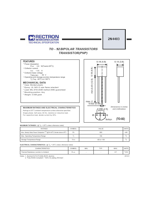
2010-5ELECTRICAL CHARACTERISTICS ( @ T A = 25C unless otherwise noted)MAXIMUM TATINGES ( @ T A = 25C unless otherwise noted)Notes :CHARACTERISTICSSYMBOL UNITS417oC/WThermal Resistance Junction to AmbientRATINGSMax. Steady State Power Dissipation (1) @TA=25oC Derate above 25CMax. Operating Temperature Range Storage Temperature RangeSYMBOL P D T J T STGR q JAVALUE MAX.-TYP.-MIN.UNITS mW6001. Alumina=0.4*0.3*0.024in.99.5% alumina2. "Fully ROHS Compliant", "100% Sn plating (Pb-free)".150-55 to +150o C oCTRANSISTOR(PNP)ELECTRICAL CHARACTERISTICS(@TA=25O C unless otherwise noted)OFF CHARACTERISTICSON CHARACTERISTICS (1)ChatacteristicCollector-Emitter Breakdown Voltage(1) (I C = -1.0 mAdc, I B = 0) Collector-Base Breakdown Voltage (I C = -0.1mAdc, I E = 0)Emitter-Base Breakdown Voltage (I E = -0.1mAdc, I C = 0)Base Cutoff Current (V CE = -35Vdc, V BE(off)= -0.4Vdc)Collector Cutoff Current (V CE = -35Vdc, V EB = -0.4Vdc)DC Current Gain (I C = -0.1mAdc, V CE = -1.0Vdc)(I C = -10mAdc, V CE = -1.0Vdc)(I C = -1.0mAdc, V CE = -1.0Vdc)V (BR)CEO -40-Vdc V (BR)CBO -40-Vdc V (BR)EBO-5.0-Vdc I CEXI BEV --0.1--0.1hFE30--60-100-100300uAdcuAdc Symbol Min Max Unit(I C = -150mAdc, V CE = -2.0Vdc)Collector-Emitter Saturation Voltage (1) (I C = -150mAdc, I B = -15mAdc)(I C = -500mAdc, I B = -50mAdc)(I C = -500mAdc, V CE = -2.0Vdc)Vdc V CE(sat)20---0.4--0.75VdcV BE(sat)-0.75-0.95--1.3Base-Emitter Saturation Voltage (1) (I C = -150mAdc, I B = -15mAdc)(I C = -500mAdc, I B =-50mAdc)SMALL-SIGNAL CHARACTERISTICSSWITCHING CHARACTERISTICSf T 200-MHz Current-Gain-Bandwidth Product (I C = -20mAdc, V CE = -10Vdc, f= 100MHz)C cb C eb -8.5pF pF t d t r t s t f----nsnsh ie -301.515kohms h re 0.18.060500X 10-4h fe 1.0100-h oe225301520umhosOutput Capacitance (V CB = -10Vdc, I E = 0, f= 1.0MHz)Input Capacitance (V EB = -0.5Vdc, I C = 0, f= 1.0MHz)Voltage Feedback Ratio (V CE = -10Vdc, I C = -1.0mAdc, f= 1.0kHz)Output Admittance (V CE = -10Vdc, I C = -1.0mAdc, f= 1.0kHz)(V CC = -30Vdc, V EB = -2.0Vdc, I C = -150mAdc, I B1= -15mAdc)(V CC = -30Vdc, I C = -150mAdc, I B1= I B2= -15mAdc)Input lmpedance (V CE = -10Vdc, I C = -1.0mAdc, f= 1.0kHz)Small-Signal Current Gain (V CE = -10Vdc, I C = -1.0mAdc, f= 1.0kHz)Delay Time Rise Time Storage Time Fall TimeNote :Pulse Test: Pulse Width <300ms,Duty Cycle <2.0%--RATING AND CHARACTERISTICS CURVES ( )Figure 1. CapacitancesFigure 3. Turn-On TimeFigure 5. Storage Time0.1 0.2 0.3 0.5 0.7 1.0 2.0 3.0 5.0 10 20 3010 20 30 50 70 100 200 300 500C A P A C I T A N C E (p F )t s ',S T O R A G E T I M E (n s )t , T I M E (n s )t , T I M E (n s )Q , C H A R G E (n C )REVERSE VOLTAGE (V)I C ,COLLECTOR CURRENT (mA)I C , COLLECTOR CURRENT (mA)I C ,COLLECTOR CURRENT (mA)Figure 4. Rise Times10203050701007.05.010 20 30 50 70 100 200 300 50010 20 30 50 70 100 200 300 500I C ,COLLECTOR CURRENT (mA)10 20 30 50 70 100 200 300 500Figure 2. Charge Data0.20.30.50.71.0100.12.03.05.07.025OC100O C2N4403RATING AND CHARACTERISTICS CURVES ()h o e , O U T P U T A D M I T T A N C E (u m h o s )h r e , V O L T A G E F E E D B A C K R A T I O (X 10-4)0.1 0.2 0.3 0.5 0.7 1.0 2.0 3.0 5.0 7.0 100.1 0.2 0.3 0.5 0.7 1.0 2.0 3.0 5.0 7.0 1050 100 200 500 1.0k 2.0k 5.0k 10k 20k 50kN F , N O I S E F I G U R E (d B )N F ,N O I S E F I G U R E (d B )Figure 6.Frequency EffectsI C , COLLECTOR CURRENT (mAdc)I C , COLLECTOR CURRENT (mAdc)Figure 8.Cuttent GainFigure 9.Input ImpedanceR S , SOURCE RESISTANCE (OHMS)Figure 7.Source Resistance EffectsI C , COLLECTOR CURRENT (mAdc)I C , COLLECTOR CURRENT (mAdc)Figure 11.Temperature CoefficientsFigure 10.Voltage Feedback Ratio 0.1 0.2 0.3 0.5 0.7 1.0 2.0 3.0 5.0 7.0 100.1 0.2 0.3 0.5 0.7 1.0 2.0 3.0 5.0 7.0 10f, FREQUENCY (KHz)46810200.01 0.02 0.05 0.1 0.2 0.5 1.0 2.0 5.0 10 20 50 100V CE = -10Vdc, T A = 25CBandwidth = 1.0Hz2N4403RATING AND CHARACTERISTICS CURVES ()Figure 12. DC Current GainFigure 13. Collector Saturation RegionFigure 14. "ON" Voltages Figure 15. Temperature Coefficients0.1 0.2 0.3 0.5 0.7 1.0 2.0 3.0 5.0 7.0 10 20 30 50 70 100 200 300 5000.005 0.01 0.02 0.03 0.05 0.07 0.1 0.2 0.3 0.5 0.7 1.0 2.0 3.0 5.0 7.0 10 20 30 500.1 0..2 0.5 1.0 2.0 5.0 10 20 50 100 200 5000.1 0..2 0.5 1.0 2.0 5.0 10 20 50 100 200 500h F E , N O R M A L I Z E D C U R R E N T G A I NV C E , C O L L E C T O R - E M I T T E R V O L T A G E (V )V O L T A G E (V )C O E F F I C I E N T (m V /OC )I C , COLLECTOR CURRENT (mA)I B , BASE CURRENT (mA)I C , COLLECTOR CURRENT (mA)I C , COLLECTOR CURRENT (mA)0.40.60.81.00.20.30.50.71.03.00.22.030442NRectron Inc reserves the right to make changes without notice to any productspecification herein, to make corrections, modifications, enhancements or other changes. Rectron Inc or anyone on its behalf assumes no responsibility or liabi- lity for any errors or inaccuracies. Data sheet specifications and its information contained are intended to provide a product description only. "Typical" paramet- ers which may be included on RECTRON data sheets and/ or specifications ca- n and do vary in different applications and actual performance may vary over ti- me. Rectron Inc does not assume any liability arising out of the application or use of any product or circuit.Rectron products are not designed, intended or authorized for use in medical, life-saving implant or other applications intended for life-sustaining or other rela- ted applications where a failure or malfunction of component or circuitry may di- rectly or indirectly cause injury or threaten a life without expressed written appr- oval of Rectron Inc. Customers using or selling Rectron components for use in such applications do so at their own risk and shall agree to fully indemnify Rect- ron Inc and its subsidiaries harmless against all claims, damages and expendit- ures.DISCLAIMER NOTICE。
November 2006 Rev 11/7EMIF02-MIC03C22 line EMI filter and ESD protectionMain product characteristicsWhere EMI filtering in ESD sensitive equipment isrequired:■Mobile phones and communication systems ■Computers and printers and MCU BoardsDescription The EMIF02-MIC03C2 is a highly integrateddevice designed to suppress EMI/RFI noise in all systems subjected to electromagneticinterference. The Flip-Chip packaging means the package size is equal to the die size.This filter includes ESD protection circuitry, which prevents damage to the application when it is subjected to ESD surges up to 15 kV .Benefits ■EMI symmetrical (I/O) low-pass filter ■High efficiency EMI filter (-35 dB @ 900 MHz)■Very low PCB space consumption: 1.07 mm x 1.47 mm■Very thin package: 0.695 mm■Coating resin on back side and lead free package■High efficiency in ESD suppression■High reliability offered by monolithic integration ■High reduction of parasitic elements through integration and wafer level packaging.Complies with following standards:IEC 61000-4-2MIL STD 883G - Method 3015-7 Class 3level 4 input pins15 kV(air discharge)8 kV (contact discharge level 1 output pins 2 kV (air discharge)2 kV(contact dischargeCoated Flip-Chip package (about 20 times real size)Ob s o l e t e P r o d uc t (s ) - P r od u c t (s ) O b s o le t e P r o d u c t (s ) - b s o l e t e P r o d u c t (s )Ob s o l e t e P r o d uc t (s ) Characteristics EMIF02-MIC03C22/71 CharacteristicsTable 1.Absolute ratings (limiting values)Symbol ParameterValue Unit T jMaximum junction temperature 125°CT opOperating temperature range -40 to +85°CT stgStorage temperature range-55 to +150°CSymbol Test conditions Min Typ Max Unit V BR I R = 1 mA68VI RMV RM = 3 V per line500nA R I/O Tolerance 68ΩC lineV R = 0 V100pFO b s o l b s o l e t e P r o d u cO b s o l e t e P r o d u c t (s ) EMIF02-MIC03C2Characteristics3/7Figure 4.ESD response to IEC 61000-4-2 (+15kV air discharge) on one input V in and one output V outFigure 5.ESD response to IEC 61000-4-2 (-15kV air discharge) on one input V in and one output V outFigure 6.Line capacitance versus applied u c t (s ) - O b s o l e t e P r o d u cO b s ol e te Pr o du ct(s)-O bs ol e te Pr o du cCharacteristics EMIF02-MIC03C24/7Figure 8.Aplac parametersaplacvar Rmic68aplacvar Lmic10paplacvar Cdiode1 100pFaplacvar Cdiode2 3.6pFaplacvar Cdiode3 1.17nFaplacvar Lbump50pHaplacvar Rbump20maplacvar Rsub0.5maplacvar Rgnd10maplacvar Lgnd50pHaplacvar Cgnd0.15pFaplacvar Lsub10pH Model D1CJO=Cdiode1BV=7IBV=1uIKF=1000IS=10fISR=100pN=1M=0.3333RS=0.7VJ=0.6TT=50nModel D2CJO=Cdiode2BV=7IBV=1uIKF=1000IS=10fISR=100pN=1M=0.3333RS=0.3VJ=0.6TT=50nModel D3CJO=Cdiode3BV=7IBV=1uIKF=1000IS=10fISR=100pN=1M=0.3333RS=0.12VJ=0.6TT=50nO b s ol e te Pr o du ct(s)-O bs ol e teO b s o ld u c t (s )EMIF02-MIC03C2Ordering information scheme5/72 Ordering information scheme3 Package informationO b s o l l e t e P rOb s o l e t e Pr o d u c t (s ) - O b s o l e t e P r o d Ordering informationEMIF02-MIC03C26/7In order to meet environmental requirements, ST offers these devices in ECOPACK®packages. These packages have a lead-free second level interconnect. The category of second level interconnect is marked on the inner box label, in compliance with JEDECStandard JESD97. The maximum ratings related to soldering conditions are also marked on the inner box label. ECOPACK is an ST trademark. ECOPACK specifications are available at: .4 Ordering information5 Revision historyOrdering code Marking Package Weight Base qty Delivery modeEMIF02-MIC03C2FWFlip-Chip 2.3 mg50007” T ape and reelDate RevisionChanges28-Nov-20061Initial release.O b s o l e t e P r o d u c t (s ) - O b s o l eOb s o l e t e P r o d uc t (s ) - O b s o l e t e P r od u c t (s ) EMIF02-MIC03C27/7Please Read Carefully:Information in this document is provided solely in connection with ST products. STMicroelectronics NV and its subsidiaries (“ST”) reserve theright to make changes, corrections, modifications or improvements, to this document, and the products and services described herein at any time, without notice.All ST products are sold pursuant to ST’s terms and conditions of sale.Purchasers are solely responsible for the choice, selection and use of the ST products and services described herein, and ST assumes no liability whatsoever relating to the choice, selection or use of the ST products and services described herein.No license, express or implied, by estoppel or otherwise, to any intellectual property rights is granted under this document. If any part of this document refers to any third party products or services it shall not be deemed a license grant by ST for the use of such third party products or services, or any intellectual property contained therein or considered as a warranty covering the use in any manner whatsoever of such third party products or services or any intellectual property contained therein.UNLESS OTHERWISE SET FORTH IN ST’S TERMS AND CONDITIONS OF SALE ST DISCLAIMS ANY EXPRESS OR IMPLIED WARRANTY WITH RESPECT TO THE USE AND/OR SALE OF ST PRODUCTS INCLUDING WITHOUT LIMITATION IMPLIED WARRANTIES OF MERCHANTABILITY, FITNESS FOR A PARTICULAR PURPOSE (AND THEIR EQUIVALENTS UNDER THE LAWS OF ANY JURISDICTION), OR INFRINGEMENT OF ANY PATENT, COPYRIGHT OR OTHER INTELLECTUAL PROPERTY RIGHT.UNLESS EXPRESSLY APPROVED IN WRITING BY AN AUTHORIZED ST REPRESENTATIVE, ST PRODUCTS ARE NOT RECOMMENDED, AUTHORIZED OR WARRANTED FOR USE IN MILITARY, AIR CRAFT, SPACE, LIFE SAVING, OR LIFE SUSTAINING APPLICATIONS, NOR IN PRODUCTS OR SYSTEMS WHERE FAILURE OR MALFUNCTION MAY RESULT IN PERSONAL INJURY,DEATH, OR SEVERE PROPERTY OR ENVIRONMENTAL DAMAGE. ST PRODUCTS WHICH ARE NOT SPECIFIED AS "AUTOMOTIVE GRADE" MAY ONLY BE USED IN AUTOMOTIVE APPLICATIONS AT USER’S OWN RISK.Resale of ST products with provisions different from the statements and/or technical features set forth in this document shall immediately void any warranty granted by ST for the ST product or service described herein and shall not create or extend in any manner whatsoever, any liability of ST.ST and the ST logo are trademarks or registered trademarks of ST in various rmation in this document supersedes and replaces all information previously supplied.The ST logo is a registered trademark of STMicroelectronics. All other names are the property of their respective owners.© 2006 STMicroelectronics - All rights reservedSTMicroelectronics group of companiesAustralia - Belgium - Brazil - Canada - China - Czech Republic - Finland - France - Germany - Hong Kong - India - Israel - Italy - Japan -Malaysia - Malta - Morocco - Singapore - Spain - Sweden - Switzerland - United Kingdom - United States of AmericaO b s o l e t e P r o d u c t (s ) - O b s o l e t e P r o d u c t (s )分销商库存信息: STMEMIF02-MIC03C2。