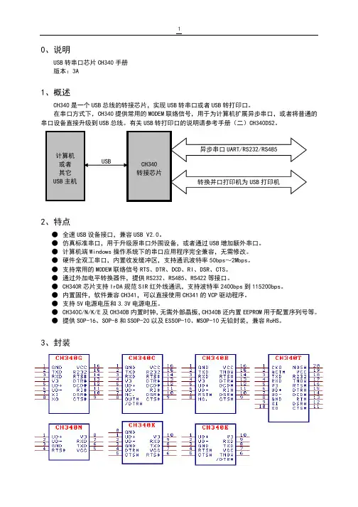
CH340 USB转串口IC 中文资料
- 格式:pdf
- 大小:138.51 KB
- 文档页数:5
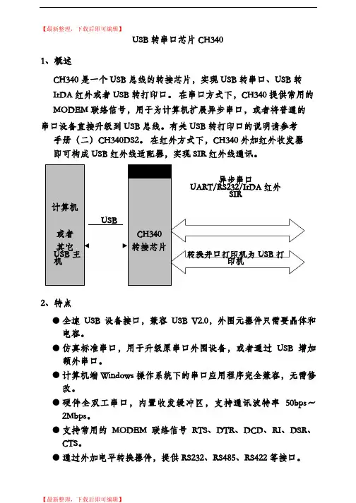
【最新整理,下载后即可编辑】USB 转串口芯片 CH3401、概述CH340 是一个 USB 总线的转接芯片,实现 USB 转串口、USB 转IrDA 红外或者 USB 转打印口。
在串口方式下,CH340 提供常用的MODEM 联络信号,用于为计算机扩展异步串口,或者将普通的串口设备直接升级到 USB 总线。
有关 USB 转打印口的说明请参考手册(二)CH340DS2。
在红外方式下,CH340 外加红外收发器即可构成 USB 红外线适配器,实现 SIR 红外线通讯。
计算机异步串口UART/RS232/IrDA 红外SIRUSB或者CH340其它转接芯片USB 主机转换并口打印机为 USB 打印机2、特点●全速USB 设备接口,兼容USB V2.0,外围元器件只需要晶体和电容。
●仿真标准串口,用于升级原串口外围设备,或者通过USB 增加额外串口。
●计算机端 Windows 操作系统下的串口应用程序完全兼容,无需修改。
●硬件全双工串口,内置收发缓冲区,支持通讯波特率50bps~2Mbps。
●支持常用的MODEM 联络信号RTS、DTR、DCD、RI、DSR、CTS。
●通过外加电平转换器件,提供 RS232、RS485、RS422 等接口。
●支持IrDA 规范SIR 红外线通讯,支持波特率2400bps 到115200bps。
●由于是通过USB 转换的串口,所以只能做到应用层兼容,而无法绝对相同。
●软件兼容 CH341,可以直接使用 CH341 的驱动程序。
●支持 5V 电源电压和 3.3V 电源电压。
●提供 SSOP-20 无铅封装,兼容 RoHS。
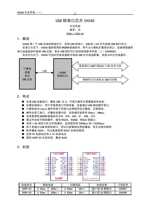
3、封装封装形式塑体宽度引脚间距封装说明订货型号SSOP-205.30mm 209mil0.65mm 25mil超小型 20 脚贴片CH340T SSOP-205.30mm 209mil0.65mm 25mil超小型 20 脚贴片CH340R4、引脚5、功能说明CH340 芯片内置了 USB 上拉电阻,UD+和 UD-引脚应该直接连接到 USB 总线上。
【CH340G】是一个USB总线的转接芯片,实现USB转串口、USB转IrDA红外或者USB转打印口。
在串口方式下,CH340G提供常用的MODEM联络信号,用于为计算机扩展异步串口,或者将普通的串口设备直接升级到USB总线。
在红外方式下,CH340G外加红外收发器即可构成USB红外线适配器,实现SIR红外线通讯。
STM32的程序下载方式因为我们现在的电脑上,已经不存在串口,所以我们一般使用USB转串口芯片,目的只有一个,把电脑的USB口映射为串口用。
常用的USB转串口芯片有CH340、CP2102、PL2303、FT232等。
我们选择哪一个呢?CH340是国产芯片,其他的是进口芯片。
CH340批量价1.5元每个,一般应用方面,性能已经足够,我使用这么多年,就没有出现过问题。
PL2303山寨货太多,买的不放心。
CP2102批量价5.2元,它是QFN封装,对于新手不易焊接。
FT232批量价在10元以上,一般用在工业级环境。
经过综合的比较,我们选择CH340作为我们开发板上使用的USB转串口芯片。
串口下载程序的过程:上电后,先把STM32的BOOT0拉高,然后就可以通过RXD和TXD引脚把要下载的程序下载到单片机,下载完程序以后,然后复位,就会运行下载到单片机中的程序。
虽然是20个引脚,不过JTAG引脚只用了6个引脚,剩下的是3.3V 和GND。
同时,STM32还支持SWD下载方式,也是在JTAG接口上,只用到了2个引脚。
无需硬件改动,只需要在程序编写软件上配置即可切换。
JTAG接口用来连接仿真器,仿真器可以是JLINK或者ULINK。
ISP和JTAG的区别:由于我们使用了USB转串口芯片,所以开发板可以直接用数据线连接电脑USB后就可以下载程序。
而JTAG,需要另外购买仿真器。
仿真器除了能够下载程序,还可以控制单片机单步运行程序或停在程序的某一条语句处,还可以随时观察单片机内部寄存器的值。
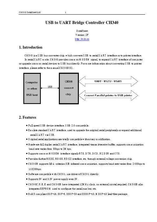
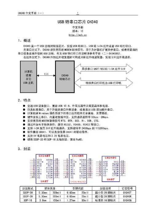
USB 转串口芯片CH340中文手册 版本:1D 1、概述CH340是一个USB 总线的转接芯片,实现USB 转串口、USB 转IrDA 红外或者USB 转打印口。
在串口方式下,CH340提供常用的MODEM 联络信号,用于为计算机扩展异步串口,或者将普通的串口设备直接升级到USB 总线。
有关USB 转打印口的说明请参考手册(二)CH340DS2。
在红外方式下,CH340外加红外收发器即可构成USB 红外线适配器,实现SIR 红外线通讯。
2、特点● 全速USB 设备接口,兼容USB V2.0,外围元器件只需要晶体和电容。
● 仿真标准串口,用于升级原串口外围设备,或者通过USB 增加额外串口。
● 计算机端Windows 操作系统下的串口应用程序完全兼容,无需修改。
● 硬件全双工串口,内置收发缓冲区,支持通讯波特率50bps ~2Mbps 。
● 支持常用的MODEM 联络信号RTS 、DTR 、DCD 、RI 、DSR 、CTS 。
● 通过外加电平转换器件,提供RS232、RS485、RS422等接口。
● 支持IrDA 规范SIR 红外线通讯,支持波特率2400bps 到115200bps 。
● 由于是通过USB 转换的串口,所以只能做到应用层兼容,而无法绝对相同。
● 软件兼容CH341,可以直接使用CH341的驱动程序。
● 支持5V 电源电压和3.3V 电源电压。
● 提供SSOP-20无铅封装,兼容RoHS 。
3、封装封装形式 塑体宽度 引脚间距 封装说明 订货型号 SSOP-20 5.30mm 209mil 0.65mm 25mil超小型20脚贴片 CH340T SSOP-205.30mm209mil0.65mm25mil超小型20脚贴片CH340R4、引脚引脚号引脚名称类型引脚说明 (括号中说明仅针对CH340R型号)19 VCC 电源正电源输入端,需要外接0.1uF电源退耦电容8 GND 电源公共接地端,直接连到USB总线的地线5 V3 电源在3.3V电源电压时连接VCC 输入外部电源,在5V电源电压时外接容量为0.01uF退耦电容9 XI 输入晶体振荡的输入端,需要外接晶体及振荡电容10 XO 输出晶体振荡的反相输出端,需要外接晶体及振荡电容6 UD+ USB信号直接连到USB总线的D+数据线7 UD- USB信号直接连到USB总线的D-数据线20 NOS# 输入禁止USB设备挂起,低电平有效,内置上拉电阻3 TXD 输出串行数据输出(CH340R型号为反相输出)4 RXD 输入串行数据输入,内置可控的上拉和下拉电阻11 CTS# 输入MODEM联络输入信号,清除发送,低(高)有效12 DSR# 输入MODEM联络输入信号,数据装置就绪,低(高)有效13 RI# 输入MODEM联络输入信号,振铃指示,低(高)有效14 DCD# 输入MODEM联络输入信号,载波检测,低(高)有效15 DTR# 输出MODEM联络输出信号,数据终端就绪,低(高)有效16 RTS# 输出MODEM联络输出信号,请求发送,低(高)有效2 ACT# 输出USB配置完成状态输出,低电平有效18 R232 输入辅助RS232使能,高电平有效,内置下拉电阻NC. 空脚CH340T:空脚,必须悬空17IR# 输入CH340R:串口模式设定输入,内置上拉电阻,低电平为SIR红外线串口,高电平为普通串口CKO 输出CH340T:时钟输出1NC. 空脚CH340R:空脚,必须悬空5、功能说明CH340芯片内置了USB上拉电阻,UD+和UD-引脚应该直接连接到USB总线上。
问题的提出。
为什么要USB转串口?昨天去看了很多电脑主板外围接口,发现现在很多主板都取消了DB25并口,甚至有些也取消了DB9串口,这是新的架构决定了。
但是现在主板都提供很多USB通道,搞电子技术开发和应用做的设备常常是ISP10并口或者232串口,所以有必要学会USB转并口、232串口、BLASTER、JTAG口的电路原理,下面是介绍CH340芯片结构的USB转串口电路,软件驱动部分以后再谈或者可以下载现成的驱动程序。
1、概述 CH340 是一个USB 总线的转接芯片,实现USB 转串口、USB 转IrDA红转打印口。
外或者USB 转打印口。
在串口方式下,CH340 提供常用的MODEM联络信号,用于为计算机扩展异步串口,(二)转打印口的说明请参考手册(二)或者将普通的串口设备直接升级到USB 总线。
有关USB 转打印口的说明请参考手册CH340DS2。
在红外方式下,CH340 外加红外收发器即可构成USB 红外线适配器,实现SIR 红外线通讯。
线通讯。
2、特点 ● 全速USB 设备接口,兼容USB V2.0,外围元器件只需要晶体和电容。
,外围元器件只需要晶体和电容。
● 仿真标准串口,用于升级原串口外围设备,或者通过USB 增加额外串口。
增加额外串口。
● 计算机端Windows 操作系统下的串口应用程序完全兼容,无需修改。
操作系统下的串口应用程序完全兼容,无需修改。
● 硬件全双工串口,内置收发缓冲区,支持通讯波特率50bps~2Mbps。
● 支持常用的MODEM 联络信号RTS、DTR、DCD、RI、DSR、CTS。
● 通过外加电平转换器件,提供RS232、RS485、RS422 等接口。
等接口。
● 支持IrDA规范SIR 红外线通讯,支持波特率2400bps 到115200bps。
● 由于是通过USB 转换的串口,所以只能做到应用层兼容,而无法绝对相同。
转换的串口,所以只能做到应用层兼容,而无法绝对相同。
0、说明USB转串口芯片CH340手册版本:3A1、概述CH340是一个USB总线的转接芯片,实现USB转串口或者USB转打印口。
在串口方式下,CH340提供常用的MODEM联络信号,用于为计算机扩展异步串口,或者将普通的串口设备直接升级到USB总线。
有关USB转打印口的说明请参考手册(二)CH340DS2。
2、特点●全速USB设备接口,兼容USB V2.0。
●仿真标准串口,用于升级原串口外围设备,或者通过USB增加额外串口。
●计算机端Windows操作系统下的串口应用程序完全兼容,无需修改。
●硬件全双工串口,内置收发缓冲区,支持通讯波特率50bps~2Mbps。
●支持常用的MODEM联络信号RTS、DTR、DCD、RI、DSR、CTS。
●通过外加电平转换器件,提供RS232、RS485、RS422等接口。
●CH340R芯片支持IrDA规范SIR红外线通讯,支持波特率2400bps到115200bps。
●内置固件,软件兼容CH341,可以直接使用CH341的VCP驱动程序。
●支持5V电源电压和3.3V电源电压。
●CH340C/N/K/E及CH340B内置时钟,无需外部晶振,CH340B还内置EEPROM用于配置序列号等。
●提供SOP-16、SOP-8和SSOP-20以及ESSOP-10、MSOP-10无铅封装,兼容RoHS。
3、封装封装形式塑体宽度引脚间距封装说明订货型号SOP-16 3.9mm 150mil 1.27mm 50mil 标准的16脚贴片CH340G SOP-16 3.9mm 150mil 1.27mm 50mil 标准的16脚贴片CH340C SOP-16 3.9mm 150mil 1.27mm 50mil 标准的16脚贴片CH340B SOP-8 3.9mm 150mil 1.27mm 50mil 标准的8脚贴片CH340N ESSOP-10 3.9mm 150mil 1.00mm 39mil 带底板的窄距10脚贴片CH340K MSOP-10 3.0mm 118mil 0.50mm 19.7mil 微小型的10脚贴片CH340E SSOP-20 5.3mm 209mil 0.65mm 25mil 缩小型20脚贴片CH340T SSOP-20 5.3mm 209mil 0.65mm 25mil 缩小型20脚贴片CH340R备注:CH340C、CH340N、CH340K、CH340E和CH340B内置时钟,无需外部晶振。
常用USB转串口芯片介绍引言USB转串口芯片是一种常见的硬件设备,广泛应用于计算机与外部串行设备之间的通信连接。
本文将介绍几种常用的USB转串口芯片,并针对它们的特性、应用领域和操作方法进行详细介绍。
CH340芯片特性•CH340芯片是一种低成本USB转串口芯片,由中国公司WCH生产。
•支持全速USB通信(12Mbps)。
•内置EEPROM,支持自定义VID/PID。
•支持5V和3.3V供电。
•可以通过使用官方提供的驱动程序在Windows、Linux和Mac OS等多种平台上使用。
应用领域•Arduino控制器和传感器模块的通信。
•工业自动化设备与计算机之间的数据传输。
•单片机与计算机的串行通信。
操作方法1.在计算机上安装CH340驱动程序。
2.将CH340芯片插入USB端口。
3.通过设备管理器(Windows)或系统信息(Mac OS)查找COM端口号。
4.使用串口通信软件进行数据传输。
PL2303芯片特性•PL2303芯片是由台湾公司Prolific Technology Inc.开发的USB转串口芯片。
•支持全速USB通信(12Mbps)。
•自动流控制和自动功耗管理。
•兼容RS-232电平标准(±5V)。
•支持5V和3.3V供电。
应用领域•GPS导航设备与计算机之间的数据传输。
•网络设备的调试和故障排除。
•打印机和POS设备的连接。
1.在计算机上安装PL2303驱动程序。
2.将PL2303芯片插入USB端口。
3.通过设备管理器(Windows)或系统信息(Mac OS)查找COM端口号。
4.使用串口通信软件进行数据传输。
FT232芯片特性•FT232芯片是由英国公司Future Technology Devices International (FTDI)开发的USB转串口芯片。
•支持高速USB通信(480Mbps)。
•内置EEPROM,支持自定义VID/PID。
•支持波特率自适应,最高可达3Mbps。
USB to UART Bridge Controller CH340DataSheetVersion: 2F1. IntroductionCH340 is a USB bus converter chip, which converts USB to serial UART interface or to printer interface.In serial UART mode, CH340 provides common MODEM signal, to expand UART interface of computer or upgrade common serial devices to USB bus directly. For more information about converting USB to printer interface, please refer to the manual CH340DS2.2. Features● Full speed USB device interface, USB 2.0 compatible.● Emulate standard UART interface, used to upgrade the original serial peripherals or expand additionalserial UART via USB.● Original serial applications are totally compatible without any modification.● Hardware full duplex serial UART interface, integrated transmit-receive buffer, supports communicationbaud rate varies from 50bps to 2Mbps.● Supports common MODEM interface signals RTS, DTR, DCD, RI, DSR and CTS.● Provides further RS232, RS485, RS422 interface, etc. through external voltage conversion chip.● CH340R supports IrDA criterion SIR infrared communication, supports baud rate varies from 2400bps to115200bps.● Software compatible with CH341, use driver of CH341 directly.● Supports 5V and 3.3V power supply even 3V.● CH340C/N/K/E and CH340B have integrated 12MHz clock, no external crystal required, CH340B alsointegrates EEPROM used to configure the serial number, etc.● RoHS compliant SOP-16, SOP-8, SSOP-20 and ESSOP-10, MSOP-10 lead-free package.3. PackagesPackage Width Of Plastic Pitch Of Pin Instruction Of PackageOrdering InformationSOP-16 3.9mm 150mil 1.27mm 50mil Small outline 16-pin patch CH340G SOP-16 3.9mm 150mil 1.27mm 50mil Small outline 16-pin patch CH340C SOP-8 3.9mm 150mil 1.27mm 50mil Small outline 8-pin patch CH340NESSOP-10 3.9mm 150mil 1.00mm 39mil Shrink Small outline 10-pin patch withbackplaneCH340KSOP-16 3.9mm 150mil 1.27mm 50mil Small outline 16-pin patch CH340B MSOP-10 3.0mm 118mil 0.50mm 19.7mil Miniature Small outline 10-pin patch CH340E SSOP-20 5.30mm 209mil 0.65mm 25mil Shrink Small outline 20-pin patch CH340T SSOP-20 5.30mm 209mil 0.65mm 25mil Shrink Small outline 20-pin patch CH340RModel differences:CH340C, CH340N, CH340K, CH340E and CH340B have integrated clock, no external crystal required.CH340B has also integrated EEPROM used to configure the serial number, etc. Some functions can be customized.The CH340K has three diodes built in to reduce current flow backwards between the I/O pins of the MCU.The backplane of the CH340K is 0# pin GND, which is an optional connection; the 3# pin GND is the necessary connection.CH340R provides reverse polarity TXD and MODEM interface signals. (Discontinued)4. Pin OutSSOP20 Pin No. SOP16Pin No.ESSOP10Pin No.SOP8Pin No.PinNamePin TypePin Description (description in bracket is only aboutCH340R)19 16 7 5 VCC POWER Power supply voltage input, requires an external0.1uF decoupling capacitor8 1 3, 0 3 GND POWER Ground5 4 10 8 V3 POWER Connect to VCC when VCC is 3V3, connect to 0.1uF decoupling capacitor when VCC is 5V9 7 NONE NONEXI INCH340T/R/G: Input of crystal oscillator, connect to12MHz crystal and capacitorNC. NONE CH340C: No Connection, must be suspended RST# INCH340B: Input of external reset, active low,integrated pull-up resistor10 8 NONE NONEXO OUTCH340T/R/G: Output of crystal oscillator, connect tocrystal and capacitorOUT# OUTCH340C: MODEM output IO, software controlled,active lowNC. NONE CH340B: No Connection, must be suspended6 5 1 1 UD+ USB signal Connect to USB D+ Signal directly7 6 2 2 UD- USB signal Connect to USB D- Signal directly20 NONE NONE NONE NOS# IN Forbid USB device suspending, active low, integratedpull-up resistor3 2 8 6 TXD OUT Transmit asynchronous data output(reverse output forCH340R)4 3 9 7 RXD IN Receive asynchronous data input, integrated configurable pull-up and pull-down resistor11 9 5 NONE CTS# IN MODEM input signal, clear to send, active low(high)12 10 NONE NONE DSR# IN MODEM input signal, data set ready, activelow(high)13 11 NONE NONE RI# IN MODEM input signal, ring indicator , activelow(high)14 12 NONE NONE DCD# IN MODEM input signal, data carrier detect, activelow(high)15 13 4 NONE DTR# OUT MODEM output signal, data terminal ready, activelow(high)16 14 6 4 RTS# OUT MODEM output signal, request to send, activelow(high)2 NONE NONE NONE ACT# OUT USB configuration completed state output, active low18 15 NONE NONE R232 IN CH340T/R/G/C: Assistant RS232 enable, active high, integrated pull-down resistor17 15 NONE NONE TNOW OUTCH340T/E/B: Ongoing data transmission statusindicator, active highIR# INCH340R:Serial mode input setting, integrated pull-upresistor, SIR infrared serial interface when low,common serial interface when high1 NONE NONE NONE CK0 OUT CH340T: clock outputNC. NONE CH340R:No Connection, must be suspended5. Function DescriptionCH340 has integrated USB pull-up resistor, UD+ and UD- pins should be connected to USB bus directly.CH340 has integrated power-on reset circuit. CH340B also provides low active external reset pin.CH340G/CH340T/CH340R need to work with 12MHz clock signal supplied to XI pin. Generally, clock signal is generated by the inverter in CH340 through crystal oscillation. The peripheral circuit needs to place a crystal of 12MHz between XI and XO, and connect to a capacitor to ground separately.CH340C, CH340N, CH340K, CH340E and CH340B have integrated clock generator, no external crystal and oscillating capacitor required.CH340B also provides EEPROM for configuring data area, product serial number and other information could be customized for each chip by specific software tools, configurable data area is shown in the table below.Byte Address AbbreviationDescription Of Chip Configuration Data Area Default00H SIG For CH340B: internal configuration information valid reg,must be 58H.For CH340H/S: external configuration information validreg, must be 53H.Invalid for other value00H01H MODE Serial mode, must be 23H 23H02H CFGSpecific configuration of chip,bit5 is used to configure product Serial Number:0= valid; 1= invalid.FEH03H WP Internal configuration information write protect flag,57Himply read only, otherwise can be rewrite00H05~04H VID Vendor ID, high byte is behind, any value. Set to 0000H or0FFFFH implies VID and PID using vendor default value1A86H07~06H PID Product ID, high byte is behind, any value 7523H 0AH PWR Max Power, The maximum supply current in 2mA units 31H17~10H SN Serial Number, the length of ASCII string is 8, disable theSerial number when the first byte is not ASCII character(21H~7FH)123456783FH~1AH PRODFor CH340B: Product String, Unicode string for productdescription. The first byte is by total bytes (less than 26H),the next byte is 03H, Unicode string after that, using vendordefault description when do not meet characteristics above.Using productdefaultdescription whenthe first byte is00HOthers (Reserved) 00H or FFHCH340 supports 5V and 3.3V power voltage. When using 5V power supply, the VCC pin connects 5V power and the V3 pin should connect with decoupling 0.1uF capacitor. When using 3.3V power supply, connects V3 with VCC, both powered with 3.3V power supply, and the other circuit voltage which connected with CH340 cannot exceed 3.3V.CH340 supports USB device suspending automatically to save power. USB device suspend is forbidden when NOS# is driven low.The DTR# pin of CH340 is used as a configuration input pin before the USB configuration completion. An external 4.7KΩ pull-down resistor can be connected with this pin to generate default low during USB enumeration, to apply larger supply current to the USB bus via the configuration descriptor for CH340.In serial UART mode, CH340 contains these pins: data transfer pins, MODEM interface signals and assistant pins.Data transfer pins contain: TXD and RXD. RXD keeps high when UART reception is idle. For CH340G/C/T/R, If pin R232 is driven high, assistant RS232 function will be enabled, an internal inverter will automatically insert to the RXD, and the pin becomes low by default. When UART transmission is idle, the TXD of CH340G/C/N/E/B/T keeps high, CH340K is weak high, while CH340R keeps low.MODEM interface signals contain: CTS#, DSR#, RI#, DCD# and RTS#, CH340C also provides OUT# pin. All these MODEM interface signals are controlled and function defined by computer applications.Assistant pins contain: IR#, R232, CK0, ACT# and TNOW. When IR# is low, infrared serial interface mode is enabled. R232 is used to control assistant RS232 function. If R232 is driven high, the RXD input will be reversed automatically. ACT# is USB device configuration complete status output (such as USB infrared adapter ready). TNOW indicates CH340 is transmitting data from UART when it is high and becomes low when transmits over. In RS485 and other half-duplex mode, TNOW could be used to indicate UART transmit-receive status. IR# and R232 are detected only once when chip powered on and reset.CH340 has integrated separate transmit-receive buffer and supports simplex, half-duplex and full duplex UART communication. Serial data contains one low-level start bit , 5, 6, 7 or 8 data bits and 1 or 2 high-level stop bits, supports odd/even/mark/space check. CH340 supports common baud rate: 50, 75, 100, 110, 134.5, 150, 300, 600, 900, 1200, 1800, 2400, 3600, 4800, 9600, 14400, 19200, 28800, 33600, 38400, 56000, 57600, 76800, 115200, 128000, 153600, 230400, 460800, 921600, 1500000, 2000000 etc.The baud rate error of CH340 UART reception allows not less than 2%, the baud rate error of CH340G/CH340T/CH340R UART transmission is less than 0.3%, less than 1% for CH340C/CH340N/CH340K/CH340E/CH340B.In the Windows OS, CH340 driver can emulate standard serial port. So the mostly original serial applications are totally compatible, without any modification.CH340 can be used to upgrade the serial interface peripherals, or expand extra serial port for computers via USB bus, through external level conversion chip provide further RS232, RS485, RS422 interface, etc.Through extra infrared transceiver, CH340R can expand SIR infrared adapter for computer via USB bus, realize infrared communication between computers and peripheral equipment that comply with IrDA specifications.6. Parameters6.1. Absolute Maximum Ratings(critical state or exceeding maximum can cause chip to not work or even be damaged)Name Parameter Description Min. Max. UnitTA Operating AmbientTemperatureCH340G/CH340T/CH340R -40 85 ℃CH340C/CH340N/CH340K/CH340E/CH340B-20 70 ℃TS Storage Temperature -55 125 ℃VCC Supply Voltage(VCC connects to power, GND to ground) -0.5 6.0 V VIO The voltage of input or output pin -0.5 VCC+0.5 V6.2. Electrical Parameters (test conditions: TA=25,VCC=5V, exclude pin℃s connected to USB bus) (all the current parameters should multiply the coefficient of 40% when the supply voltage is 3.3V)Name Parameter Description Min. Typical Max. UnitVCC Supply VoltageV3 doesn’t connect to VCC 4.0 5 5.3V V3 connects toVCCCH340G/T/R 2.8 3.3 3.6CH340C/N/K/E/B 3.1 3.3 3.6ICCOperating SupplyCurrent(Normal Operation)CH340G/C/N/K/E/T/R7 20mACH340B 6 15ISLP Operating Supply Current(USBSuspend)VCC=5V 0.1 0.2mAVCC=3.3V 0.09 0.15VIL Input Low Voltage -0.5 0.7 V VIH Input High Voltage 2.0 VCC+0.5 V VOL Output Low Voltage(4mA draw current) 0.5 VVOH Output High Voltage(3mA output current)(Output 100uA current during chip reset)VCC-0.5 VIUP Draw current of input with integrated pull-up resistor 3 150 300 uAIDN Draw current of input with integrated pull-downresistor-50 -150 -300 uAVR Voltage threshold when power-up reset 2.4 2.6 2.8 V 6.3. Timing Parameters (test conditions: TA=25,VCC=5V)℃Name Parameter Description Min. Typical Max. Unit FCLK Frequency of input clock in XI 11.98 12.00 12.02 MHz TPR Reset time of power-up 20 35 50 mS 7. Applications7.1. USB to RS232 converter configurationThe image above use CH340T/CH340B (or CH340C ) to realize USB to RS232 converter. CH340 provides common UART and MODEM signals, converts TTL to RS232 through level conversion chip U8. Port P11 is DB9 connector, the pins and their functions are the same as common PC DB9 connector, the chips similar with U8 have MAX213/ADM213/SP213/MAX211 etc.U8 and C46/C47/C48/C49/C40 could be removed when realize USB to TTL converter only. The signal lines in the image only RXD、TXD and public ground need connected, the other signal lines should suspend when not use.P2 is USB port, USB bus contains a pair of 5V power lines and a pair of data signal lines . Usually, the color of +5V power line is red, the black one is ground. D+ signal line is green and the D- signal line is white. The max supply current of USB bus is up to 500mA. Generally, CH340 and low power consumption USB products can use the 5V power supplied by USB bus directly. If the USB products supply standing power by other manner, CH340 should use this power too. If the USB bus power and standing power are necessary at the same time, connect a 1Ωresistor between USB bus 5V power line and USB products 5V standing power line, and connect the ground lines of these two power directly.The capacitor C8 on V3 is 0.1uF, used to CH340 internal power node decoupling. The capacitor C9 is 0.1uF, used to external power decoupling.For CH340G/T/R, Crystal X2, capacitor C6 and C7 are used for clock oscillation circuit. The X2 is 12MHz quartz crystal, C6 and C7 are monolithic or high frequency ceramic capacitors with 22pF. If X2 is ceramic with low cost, C6 and C7 must use the recommended value of crystal manufacturer and generally is 47pF. For the crystalwhich is difficult to oscillate, halved value is suggested for C6.For CH340C/N/K/E/B, crystal X2 and capacitor C6, C7 are not required.When designing the PCB, pay attention to: decoupling capacitor C8 and C9 must keep near to connection pin of CH340; make sure D+ and D- signal lines are parallel and provide ground or pour copper on both sides to reduce outside interference; the signal lines relevant to XI and XO should be kept as short as possible. In order to reduce the high frequency interference, around the ground or pour copper around the relevant components.7.2. USB to RS232 converter configuration (3-wire)The image below is USB to 3-wire RS232 converter design which is the most basic and most commonly used, U5 uses MAX232/ICL232/SP232 etc.7.3. USB to RS232 converter configuration (simplified version using RS232)The image above is USB to RS232 converter design too, the function of this circuit is the same with 7.2 section except the range of output RS232 is narrower. When R232 pin is driven high, the assistant RS232 function will be enabled, just need to add some diodes, transistors, resistors and capacitors, the special level conversion chip U5 in section 7.2 could be replaced and the hardware cost is lower.7.4. USB to Infrared AdapterThe image above is a USB to infrared adapter design which is composed with USB convert IrDA infrared chip CH340R and infrared transceiver U14 (ZHX1810/HSDL3000 etc). The resistor R13 is used to weaken influence of large current in infrared transmitting. The current limiting resistor R14 should be adjusted according to the manufacturer’s recommended value of the infrared transceiver U14.7.5. USB to RS485 Converter ConfigurationThe TNOW pin can be used to control DE (high active send enable) and RE# (low active receive enable) pin of RS485 transceiver.3247.6. Connect CH340 to MCU and supply power togetherThe image below is a sample design to achieve USB connection on an MCU by connecting it to a CH340 via TTL serial port. Here we use self-power mode, VCC supports 5V or 3.3V(V3 shorted to VCC if VCC is 3.3V), and don’t use USB bus power VBUS at all(Can be tested by connecting series resistor to I/O of MCU if needed).CH340 shares the same power source with MCU, hence there would be no current inrush through I/O betweenCH340 and MCU.Unused CH340 pins can be suspended. For CH340C, CH340N, CH340E, CH340B, X6 , C17 and C18 are unused.7.7. Connect CH340 to MCU and supply power separatelyThe image below is a sample design to achieve USB connection on an MCU by connecting it to a CH340 via TTL serial port. CH340 is powered by USB bus VBUS. MCU is powered by another power source VDD, VDD supports 5V, 3.3V and even 2.5V, 1.8V. The diodes D6 and D7 are used to help relieve current inrush problems between CH340 and MCU through RXD or diode within RX. The RX pin of the MCU should enable internalpull-up resistor. If not, we suggest adding an 8kΩ ~ 30kΩ pull-up resistor to RX pin.Diode D6 is meant for circumstances when CH340 is not powered but MCU is powered, and TX high level causes current inrush through RXD internal diode; Diode D7 is meant for circumstances when MCU is not powered but CH340 is powered, and TXD high level causes current inrush through RX internal diode. If certain circumstance can be ensured to be avoided, the corresponding diode can be removed. For example, if the MCU has a permanent power source, then D7 can be short-circuited.Prioritized choice for diode is low power Schottky diode. Common diode such as IN4148 is also usable. Besides, replacing the diode with an 1kΩ(better less than 2kΩ) resistor is acceptable too.Usually, we don’t recommend power CH340 and MCU separately if not necessary.7.8. Connect CH340K to MCU and supply power separatelyThe figure above shows the reference circuit for USB communication between the MCU and the CH340K via UART. CH340K is powered by the USB bus VBUS (VCC), the MCU uses another power supply VDD, whichCH340 DataSheet(1st) 11supports 5V, 3.3V or even 2.5V, 1.8V. The backplane of the CH340K package is an optional GND pin that can be easily connected to GND or left floating depending on the PCB trace.The TXD and RTS# pins of the CH340K and the RXD pin have built-in diodes to prevent current flow backwards (as shown), and a weak pull-up resistor of about 75KΩis built in to maintain the default or idle state high level (in the figure). Not marked), this can achieve low-level drive and weak high-level drive, as well as reduce current flow backwards when the CH340K and MCU are independently powered. The CH340K can completely prevent the MCU power supply from powering down the current of the CH340K, and can also greatly reduce the current flow backwards of the MCU power supply to the power-off CH340K(up to 150μA). When used for communication baud rate above 120Kbps, it is recommended to enable built-in or external 2KΩ~ 22KΩpull-up resistor for the RX pin of the MCU.The DTR# pin of the CH340K is a normal push-pull output, and the CTS# pin is a normal input with a built-in pull-up resistor. These two pins have no built-in diodes and do not have the function of preventing current flow backwards. They are generally not used to connect to the MCU.DTR# can be used to control the power switch that VCC supplies to VDD. Four power control schemes are available as shown below. The T4 scheme and the Q1 scheme (Q1 should choose a lower Vth N-OSFET) is a simplified scheme. The VDD output voltage is about VCC-0.8V and the current does not exceed 200mA. The T6 scheme and the Q3 scheme are complete solutions. In the figure, D10 and D11 are used to prevent VDD from flow backwards to VCC, which is optional.。
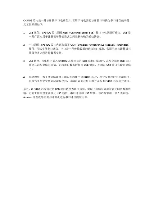
CH340G芯片是一种USB转串口电路芯片,常用于将电脑的USB接口转换为串口通信的功能。
其工作原理如下:
B通信:CH340G芯片通过USB(Universal Serial Bus)接口与电脑进行通信。
USB是
一种广泛应用于计算机和外部设备之间数据传输的通信协议。
2.串口通信:CH340G芯片内部集成了UART(Universal Asynchronous Receiver/Transmitter)
硬件,可以实现串口通信。
串口是一种传输数据的通信接口标准,常用于连接计算机与外部设备之间进行数据交换。
B转换:当电脑上插入CH340G芯片连接的USB转串口模块时,芯片会识别USB接口
并建立起与电脑的通信。
它将串口数据转换为USB数据,并通过USB接口传输到电脑上。
4.驱动程序:为了使电脑能够正确识别和使用CH340G芯片,需要安装相应的驱动程序。
在操作系统中安装好驱动程序后,电脑可以通过串口的方式与CH340G芯片进行通信。
总之,CH340G芯片通过将USB接口转换为串口通信,实现了电脑与外部设备之间的数据传输。
它的工作原理主要涉及USB通信、串口通信和USB转换。
该芯片常用于嵌入式系统、Arduino开发板等需要与计算机进行串口通信的应用中。
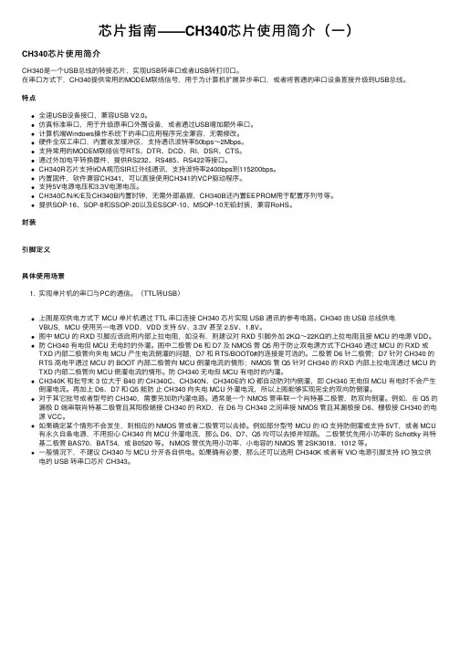
芯⽚指南——CH340芯⽚使⽤简介(⼀)CH340芯⽚使⽤简介CH340是⼀个USB总线的转接芯⽚,实现USB转串⼝或者USB转打印⼝。
在串⼝⽅式下,CH340提供常⽤的MODEM联络信号,⽤于为计算机扩展异步串⼝,或者将普通的串⼝设备直接升级到USB总线。
特点全速USB设备接⼝,兼容USB V2.0。
仿真标准串⼝,⽤于升级原串⼝外围设备,或者通过USB增加额外串⼝。
计算机端Windows操作系统下的串⼝应⽤程序完全兼容,⽆需修改。
硬件全双⼯串⼝,内置收发缓冲区,⽀持通讯波特率50bps~2Mbps。
⽀持常⽤的MODEM联络信号RTS、DTR、DCD、RI、DSR、CTS。
通过外加电平转换器件,提供RS232、RS485、RS422等接⼝。
CH340R芯⽚⽀持IrDA规范SIR红外线通讯,⽀持波特率2400bps到115200bps。
内置固件,软件兼容CH341,可以直接使⽤CH341的VCP驱动程序。
⽀持5V电源电压和3.3V电源电压。
CH340C/N/K/E及CH340B内置时钟,⽆需外部晶振,CH340B还内置EEPROM⽤于配置序列号等。
提供SOP-16、SOP-8和SSOP-20以及ESSOP-10、MSOP-10⽆铅封装,兼容RoHS。
封装引脚定义具体使⽤场景1. 实现单⽚机的串⼝与PC的通信。
(TTL转USB)上图是双供电⽅式下 MCU 单⽚机通过 TTL 串⼝连接 CH340 芯⽚实现 USB 通讯的参考电路。
CH340 由 USB 总线供电VBUS,MCU 使⽤另⼀电源 VDD,VDD ⽀持 5V、3.3V 甚⾄ 2.5V、1.8V。
图中 MCU 的 RXD 引脚应该启⽤内部上拉电阻,如没有,则建议对 RXD 引脚外加 2KΩ~22KΩ的上拉电阻且接 MCU 的电源 VDD。
防 CH340 有电但 MCU ⽆电时的外灌。
图中⼆极管 D6 和 D7 及 NMOS 管 Q5 ⽤于防⽌双电源⽅式下CH340 通过 MCU 的 RXD 或TXD 内部⼆极管向失电 MCU 产⽣电流倒灌的问题,D7 和 RTS/BOOT0#的连接是可选的。
[ch340g]是USB总线适配器芯片,可以将USB转换为串行端口,将USB转换为IrDA红外或将USB转换为打印端口。
ch340g在串行端口模式下提供公共调制解调器联系信号,用于扩展计算机的异步串行端口,或将普通串行设备直接升级为USB总线。
在红外模式下,ch340g加上红外收发器可以组成USB红外适配器以实现Sir红外通信。
STM32程序的下载方法因为我们的计算机现在没有串行端口,所以我们一般使用USB到串行芯片,目的只有一个,计算机的USB端口映射为串行端口。
常用的USB转串行芯片为ch340,CP2102,PL2303,ft232等。
我们应该选择哪一个?Ch340是国产芯片,其他是进口芯片。
Ch340每批的价格为1.5元,一般应用,性能已经足够,我使用了这么多年,一直没有问题。
PL2303的假冒商品太多,所以我不敢购买。
CP2102批量价格为5.2元,它是QFN 封装,对于新手来说不容易焊接。
Ft232的批量价格在10元以上,一般用于工业环境。
经过全面比较,我们选择ch340作为开发板上使用的USB转串口芯片。
通过串口下载程序的过程:上电后,先拉起STM32的boot0,再通过RXD和TXD引脚下载要下载的程序到MCU。
下载程序后,然后重置,将运行下载到MCU的程序。
尽管有20个引脚,但JTAG引脚仅使用6个引脚,其余分别为3.3V和GND。
同时,STM32还支持SWD下载模式,该模式仅在JTAG接口上使用两个引脚。
无需更改硬件,仅需在编程软件上进行配置即可进行切换。
JTAG接口用于连接仿真器,可以是JLINK或ULINK。
ISP和JTAG之间的区别:因为我们使用USB到串行芯片,所以开发板可以将计算机USB与数据电缆直接连接,然后下载程序。
另一方面,JTAG 需要购买一个仿真器。
模拟器不仅可以下载程序,还可以控制MCU 逐步运行程序或在程序的特定语句处停止,还可以随时观察MCU内部寄存器的值。
USB to serial chip CH340English DataSheet Version: 2C1 IntroductionCH340 is a USB bus conversion chip, it can realize USB to UART interface or USB to printer interface.In serial UART mode, CH340 provides common MODEM liaison signal, used to expand UART interface of computer or upgrade the common serial device to USB bus directly. For more information on USB conversion to printer interface please refer to the manual CH340DS2.2 Features●Full speed USB device interface, compatible with USB V2.0.●Emulate standard UART interface, used to upgrade the serial peripherals, or expand UART interface viaUSB bus.●Original serial applications are totally compatible, without any modification in Windows operation system.●Hardware full duplex serial UART interface, built-in transmit-receive buffer, supports communication baudrate varies from 50bps to 2Mbps.●Supports common MODEM liaison signal RTS, DTR, DCD, RI, DSR and CTS.●Through external level conversion chip provide further RS232, RS485, RS422 interface, etc.●CH340R supports IrDA criterion SIR infrared communication, supports baud rate varies from 2400bps to 115200bps.●Software compatible with CH341, use driver of CH341 directly.●Support 5V and 3.3V power supply even 3V.●CH340C, CH340E and CH340B have built-in crystal, no external crystal, CH340B also integratesEEPROM used to configure the serial number, etc.●SOP-16 and SSOP-20 and MSOP-10 lead-free RoHS compliant package.3 PackagePackage shape Width of plastic Pitch of Pin Instruction of package Ordering type SOP-16 3.9mm150mil 1.27mm50mil Small outline package of 16-pin CH340G SOP-16 3.9mm150mil 1.27mm50mil Small outline package of 16-pin CH340C SOP-16 3.9mm150mil 1.27mm50mil Small outline package of 16-pin CH340B MSOP-10 3.0mm118mil0.50mm19.7mil Shrink small outline package of 10-pin CH340E SSOP-20 5.30mm209mil0.65mm25mil Shrink small outline package of 20-pin CH340T SSOP-20 5.30mm209mil0.65mm25mil Shrink small outline package of 20-pin CH340RModel differences:CH340C, CH340E and CH340B have built-in crystal, no external crystal;CH340B also has built-in EEPROM used to configure the serial number,etc.Some functions can be customized. CH340R provides reverse polarity TXD and MODEM signals. (No spot)4.PinsSSOP20 Pin No.SOP16Pin No.MSOP10Pin No.Pin Name Pin TypePin Description (description in bracket is only aboutCH340R)19167VCC POWER Positive power input port, requires an external 0.1uF powerdecoupling capacitor813GND POWER Public ground, ground connection for USB54NONE V3POWER Connect to VCC to input external power when 3.3V power supply, connect to 0.1uF decoupling capacitor when 5Vpower supplyXI IN CH340T/R/G: Input of crystal oscillator, connect to crystaland capacitorNC.NONE CH340C: No Connection, must be suspended 97NONERST#IN CH340B: Input of external reset, active low, built-inThe Data Sheet of CH340 (the first) 3pull-up resistorXO OUT CH340T/R/G: Output of crystal oscillator, connect tocrystal and capacitor108NONENC.NONE CH340C/B: No Connection, must be suspended 651UD+USB signal Directly connect to D+ data wire of USB bus 762UD-USB signal Directly connect to D- data wire of USB bus20NONE NONE NOS#IN Forbid USB device suspending, active low, built-in pull-upresistor328TXD OUT Transmit asynchronous data output(reverse output forCH340R)439RXD IN Receive asynchronous data input, built-in configurable pull-up and pull-down resistor1195CTS#IN MODEM liaison input signal, clear to send, activelow(high)1210NONE DSR#IN MODEM liaison input signal, data set ready, activelow(high)1311NONE RI#IN MODEM liaison input signal, ring indicator , activelow(high)1412NONE DCD#IN MODEM liaison input signal, data carrier detect, activelow(high)1513NONE DTR#OUT MODEM liaison output signal, data terminal ready, activelow(high)16144RTS#OUT MODEM liaison output signal, request to send, activelow(high)2NONE NONE ACT#OUT USB configuration completed state output, active low1815NONE R232IN CH340T/R/G/C: Assistant RS232 enable, active high,built-in pull-down resistorTNOW OUT CH340T/E/B: Ongoing data transmission status indicator,active high17156IR#IN CH340R:Serial mode input setting, built-in pull-up resistor, SIR infrared serial interface when low, common serialinterface when highCK0OUT CH340T: clock output 1NONE NONENC.NONE CH340R:No Connection, must be suspend5.Function DescriptionCH340 chip has built-in USB pull-up resistor, UD+ and UD- pins must be connected to USB bus directly.CH340 chip has built-in power-on reset circuit. CH340B also provides low active external reset pin.CH340G/CH340T/CH340R chips need to work with 12MHz clock signal supplied to XI pin. Generally, clock signal is generated crystal oscillation with inverter in CH340. The peripheral circuit needs to place a crystal of 12MHz between XI and XO, and connect to a capacitor to ground separately.CH340C, CH340E and CH340B chip have built-in clock generator, no external crystal and oscillating capacitor required.CH340B chip also provides EEPROM for configuring data area, product serial number and other information could be customized for each chip by specific software tools, configurable data area is shown in the table below.Byte Address AbbreviationDescription of chip configuration data area Default00H SIG For CH340B: Internal configuration information valid reg,must be 58H.For CH340H/S: External configuration information validreg, must be 53H.Invalid for other value00H01H MODE Serial mode, must be 23H23H02H CFGSpecific configuration of chip,bit5 is used to configure product Serial Number:0= valid; 1= invalid.FEH03H WP Internal configuration information write protect flag,57Himply read only, otherwise can be rewrite00H05~04H VID V endor ID, high byte is behind, any value. Set to 0000H or0FFFFH implies VID and PID using vendor default value1A86H07~06H PID Product ID, high byte is behind, any value7523H 0AH PWR Max Power, The maximum supply current in 2mA units31H17~10H SN Serial Number, the length of ASCII string is 8, disable theSerial number when the first byte is not ASCII character(21H~7FH)123456783FH~1AH PROD For CH340B: Product String, Unicode string for Productdescription. The first byte is by total bytes (less than 26H),the next byte is 03H, Unicode string after that, using vendordefault description when do not meet characteristics above.Using productdefault description when the first byte is00HOthers(Reserved unit)00H or FFHCH340 chip supports 5V and 3.3V power voltage. When using 5V source power, the VCC pin input 5V power and the V3 pin should connect with decoupling 0.1uF capacitor. When using 3.3V power voltage, connects V3 with VCC, both input 3.3V power voltage, and the other circuit voltage which connected with CH340 cannot exceed 3.3V.CH340 supports USB device suspending automatically to save power. USB device suspend is forbidden when NOS# is driven low.The DTR# pin of CH340 is used as a configuration input pin before the USB configuration is complete. An external 4.7KΩ pull-down resistor can be connected with this pin to generate default low level during USB enumeration, apply larger supply current to the USB bus via the configuration descriptor.In UART mode, CH340 chip contains these pins: data transfer pins, MODEM liaison signal pins and assistant pins.Data transfer pins contain: TXD and RXD pin. RXD keeps high when UART reception is idle. For CH340G/C/T/R chip, If R232 pin is driven high, assistant RS232 function will be enabled, an internal inverter will automatically insert to the RXD pin , and the pin becomes low by default. When UART transmission is idle, the TXD pin of CH340G/C/B/T keeps high, while CH340R keeps low. MODEM liaison signal pins contain: CTS#, DSR#, RI#, DCD# and RTS#. All these MODEM liaison signal are controlled and function defined by computer applications.Assistant pins contain: IR#, R232, CK0, ACT# and TNOW. When IR# is low-level, infrared serial interface mode is enabled. R232 pin is used to control assistant RS232 function. If R232 pin is driven high, the RXD pin input will be reversed automatically. ACT# pin is USB device configuration complete status output (such as USB infrared adapter ready). TNOW pin indicates CH340 is transmitting data from UART when it is high-level and becomes low when transmit over. In RS485 and other half-duplex mode, TNOW could be used to indicate UART transmit-receive status. IR# and R232 are detected only once when chip powered on and reset.CH340 has built-in separate transmit-receive buffer and supports simplex, half-duplex and full duplex UART communication. Serial data contains one low-level start bit , 5, 6, 7 or 8 data bits and 1 or 2 high-level stop bits, supports odd/even/mark/space check. CH340 supports common baud rate: 50, 75, 100, 110, 134.5, 150, 300, 600, 900, 1200, 1800, 2400, 3600, 4800, 9600, 14400, 19200, 33600, 38400, 56000, 57600, 76800, 115200, 128000, 153600, 230400, 460800, 921600, 1500000, 2000000 etc.The baud rate error of CH340 UART reception allows not less than 2%, the baud rate error of CH340G/CH340T/CH340R UART transmission is less than 0.3%, less than 1% for CH340C/CH340E/ CH340B.In the Windows operation system, CH340 driver can emulate standard serial port. So the mostly original serial applications are totally compatible, without any modification.CH340 can be used to upgrade the serial interface peripherals, or expand extra serial port for computers via USB bus, through external level conversion chip provide further RS232, RS485, RS422 interface, etc.Only need to add infrared transceiver, CH340R can expand SIR infrared adapter for computer via USB bus, realize infrared communication between computer and peripheral equipment that comply with IrDA specifications.6.Parameter6.1 Absolute maximum rating (Critical or exceeding absolute maximum can cause permanent damage to device)Name Parameter Description Min.Max.UnitsCH340G/CH340T/CH340R-4085℃TA Ambient temperatureCH340C/CH340E/CH340B-2070℃TS Storage temperature-55125℃VCC Supply V oltage(VCC connects to power, GND to ground)-0.5 6.0VVIO The voltage of input or output pin-0.5VCC+0.5V6.2. Electrical Parameter (test conditions: TA=25℃, VCC=5V, exclude pin connected to USB bus)(All the current parameters should multiply the coefficient of 40% when the power is 3.3V)NameParameter DescriptionMin. Typical Max. Units V3 doesn’t connect to VCC 4.0 5 5.3 CH340G/T/R 2.8 3.3 3.6 VCC Supply V oltageV3 connect toVCCCH340C/E/B 3.03.3 3.6 VCH340G/C/E/T/R7 20 ICCOperating Supply Current(Normal Operation)CH340B 6 15 mA VCC=5V 0.1 0.2 ISLPOperating Supply Current(USBSuspend) VCC=3.3V0.090.15 mA VIL Low-level Input V oltage -0.5 0.7 V VIH High-level Input V oltage2.0 VCC+0.5 V VOL Low-level Output V oltage(4mA draw current) 0.5V VOH High-level Output V oltage(3mA output current) (Output 100uA current during chip reset) VCC-0.5 V IUP Input current input with built-in pull-up resistor 3 150 300 uA IDN Input current input with built-in pull-down resistor-50 -150 -300 uA VRRestrict voltage when power-up reset2.42.62.8V6.3. Sequence Parameter (test conditions: TA=25℃,VCC=5V)Name Parameter Description Min. Typical Max. Units FCLK Frequency of input clock in XI 11.98 12.00 12.02 MHz TPRReset time of power-up203550mS7.Application7.1.1 USB to RS232 Converter Configuration using CH340T7.1.2 USB to RS232 Converter Configuration using CH340BThe image above use CH340T/CH340B (or CH340C ) to realize USB to RS232 converter. CH340 provides common UART and MODEM signal, converts TTL to RS232 through level conversion chip U8. Port P11 is DB9 connector, the pin and its function are the same as common PC DB9 connector, the chips similar withU8 have MAX213/ADM213/SP213/MAX211 etc.U8 and C46/C47/C48/C49/C40 could be removed when realize USB to TTL converter only. The signal lines in the image only RXD、TXD and public ground need connected, the other signal lines should suspend when not use.P2 is USB port, USB bus contains a pair of 5V power lines and a pair of data signal lines . Usually, the color of +5V power line is red, the black one is ground. D+ signal line is green and the D- signal line is white. The max supply current of USB bus is up to 500mA. Generally, CH340 and low power consumption USB products can use the 5V power supplied by USB bus directly. If the USB products supply standing power by other manner, CH340 should use this power too. If the USB bus power and standing power are necessary at the same time, connect a 1Ω resistor between USB bus 5V power line and USB products 5V standing power line, and connect the ground lines of these two power directly.The capacitor C8 on V3 pin is 0.1uF, used to CH340 internal power node decoupling. The capacitor C9 is 0.1uF, used to external power decoupling.For CH340G/T/R chip, Crystal X2, capacitor C6 and C7 are used for clock oscillation circuit. The X2 is 12MHz quartz crystal, C6 and C7 are monolithic or high frequency ceramic capacitors with 22pF. If X2 is ceramic with low cost, C6 and C7 must use the recommended value of crystal manufacturer and generally is 47pF. For the crystal which is difficult to oscillate, halved value is suggested for C6.For CH340C/E/B chip, crystal X2 and capacitor C6, C7 are not required.When designing the PCB, pay attention to: decoupling capacitor C8 and C9 must keep near to connection pin of CH340; makes sure D+ and D- signal lines are parallel and supply ground lines or pour copper beside them to decrease the interference from outside signal; the signal lines relevant to XI and XO should be kept as short as possible. In order to lessen the high frequency interference, around the ground wire or pour copper around the relevant components.7.2. USB to RS232 Converter Configuration (3-wire)The image below is USB to 3-wire RS232 converter design which is the most basic and most commonly used, U5 uses MAX232/ICL232/SP232 etc.7.3 USB to RS232 Converter Configuration (Simplified version using R232)The image above is USB to RS232 converter design too, the function of this circuit is the same with 7.2 section except the range of output RS232 is narrower. When R232 pin is driven high, the assistant RS232 function will be enabled, just need to add some diodes, transistors, resistors and capacitors, the special level conversion chip U5 in section 7.2 could be replaced and the hardware cost is lower.7.4 USB to Infrared AdapterThe image above is USB to infrared adapter design is composed with USB convert IrDA infrared chip CH340R and infrared transceiver U14 (ZHX1810/HSDL3000 etc).The resistor R13 is used to weaken influence of large current in infrared transmitting. The current limiting resistor R14 should be adjusted according to the manufacturer’s recommended value of the infrared transceiver U14.7.5. USB to RS485 Converter ConfigurationThe TNOW pin can be used to control DE (high active send enable) and RE# (low active receive enable)pin of RS485 transceiver.。
ch340g芯片资料CH340 是一个USB 总线的转接芯片,实现USB 转串口、USB 转IrDA 红外或者USB 转打印口。
提供了三种常用USB接口,便于连接,并将所有IO引出●全速USB 设备接口,兼容USB V2.0。
●仿真标准串口,用于升级原串口外围设备,或者通过USB增加额外串口。
●计算机端Windows 操作系统下的串口应用程序完全兼容,无需修改。
●硬件全双工串口,内置收发缓冲区,支持通讯波特率50bps~2Mbps。
●支持常用的MODEM 联络信号RTS、DTR、DCD、RI、DSR、CTS。
●通过外加电平转换器件,提供RS232、RS485、RS422 等接口。
●软件兼容CH341,可以直接使用CH341的驱动程序。
●支持5V 电源电压和3.3V电源电压甚至3V 电源电压。
●CH340C/CH340B 内置时钟,无需外部晶振●提供SOP-16 封装CH340G】是一个USB总线的转接芯片,实现USB转串口、USB 转IrDA红外或者USB转打印口。
在串口方式下,CH340G提供常用的MODEM联络信号,用于为计算机扩展异步串口,或者将普通的串口设备直接升级到USB总线。
在红外方式下,CH340G外加红外收发器即可构成USB红外线适配器,实现SIR红外线通讯。
CH340系列usb转串口驱动是为CH340系列推出的一款免费的驱动程序,多数的芯片都是CH340芯片,所以此款驱动适用于大部分的USB转串口,兼容win7、win8、win10等操作系统CH340G-CH340 64位驱动支持win10/win7安装前,先卸载老的驱动!安装的时候,不要插340的串口!特点:全速USB设备接口,兼容USBV2.0,外围元器件只需要晶体和电容。
仿真标准串口,用于升级原串口外围设备,或者通过USB 增加额外串口。
计算机端Windows操作系统下的串口应用程序完全兼容,无需修改。
硬件全双工串口,内置收发缓冲区,支持通讯波特率50bps~2Mbps。
USB转串口芯片CH340手册版本:2B1、概述CH340是一个USB总线的转接芯片,实现USB转串口或者USB转打印口。
在串口方式下,CH340提供常用的MODEM联络信号,用于为计算机扩展异步串口,或者将普通的串口设备直接升级到USB总线。
有关USB转打印口的说明请参考手册(二)CH340DS2。
2、特点●全速USB设备接口,兼容USB V2.0。
●仿真标准串口,用于升级原串口外围设备,或者通过USB增加额外串口。
●计算机端Windows操作系统下的串口应用程序完全兼容,无需修改。
●硬件全双工串口,内置收发缓冲区,支持通讯波特率50bps~2Mbps。
●支持常用的MODEM联络信号RTS、DTR、DCD、RI、DSR、CTS。
●通过外加电平转换器件,提供RS232、RS485、RS422等接口。
●CH340R芯片支持IrDA规范SIR红外线通讯,支持波特率2400bps到115200bps。
●软件兼容CH341,可以直接使用CH341的驱动程序。
●支持5V电源电压和3.3V电源电压甚至3V电源电压。
●CH340C和CH340B内置时钟,无需外部晶振,CH340B还内置EEPROM用于配置序列号等。
●提供SOP-16和SSOP-20无铅封装,兼容RoHS。
3、封装封装形式塑体宽度引脚间距封装说明订货型号SOP-16 3.9mm 150mil 1.27mm 50mil 标准的16脚贴片CH340G SOP-16 3.9mm 150mil 1.27mm 50mil 标准的16脚贴片CH340C SOP-16 3.9mm 150mil 1.27mm 50mil 标准的16脚贴片CH340B SSOP-20 5.30mm 209mil 0.65mm 25mil 超小型20脚贴片CH340T SSOP-20 5.30mm 209mil 0.65mm 25mil 超小型20脚贴片CH340R 型号区别:CH340C和CH340B内置时钟,无需外部晶振。
USB 转串口芯片CH340中文手册 版本:1B 1、概述CH340是一个USB 总线的转接芯片,实现USB 转串口、USB 转IrDA 红外或者USB 转打印口。
在串口方式下,CH340提供常用的MODEM 联络信号,用于为计算机扩展异步串口,或者将普通的串口设备直接升级到USB 总线。
有关USB 转打印口的说明请参考手册(二)CH340DS2。
在红外方式下,CH340外加红外收发器即可构成USB 红外线适配器,实现SIR 红外线通讯。
2、特点● 全速USB 设备接口,兼容USB V2.0,外围元器件只需要晶体和电容。
● 仿真标准串口,用于升级原串口外围设备,或者通过USB 增加额外串口。
● 计算机端Windows 操作系统下的串口应用程序完全兼容,无需修改。
● 硬件全双工串口,内置收发缓冲区,支持通讯波特率50bps ~2Mbps 。
● 支持常用的MODEM 联络信号RTS 、DTR 、DCD 、RI 、DSR 、CTS 。
● 通过外加电平转换器件,提供RS232、RS485、RS422等接口。
● 支持IrDA 规范SIR 红外线通讯,支持波特率2400bps 到115200bps 。
● 由于是通过USB 转换的串口,所以只能做到应用层兼容,而无法绝对相同。
● 软件兼容CH341,可以直接使用CH341的驱动程序。
● 提供SSOP-20和SOP-20无铅封装,兼容RoHS 。
3、封装封装形式 塑体宽度 引脚间距 封装说明 订货型号 SOP-20 7.62mm 300mil 1.27mm50mil 标准的宽20脚贴片 CH340H SSOP-20 5.30mm 209mil 0.65mm 25mil 超小型20脚贴片 CH340T SSOP-205.30mm209mil0.65mm25mil超小型20脚贴片CH340R4、引脚引脚号引脚名称类型引脚说明 (括号中说明仅针对CH340R型号)19 VCC 电源正电源输入端,需要外接0.1uF电源退耦电容8 GND 电源公共接地端,直接连到USB总线的地线5 V3 电源在5V电源电压时外接容量为0.01uF退耦电容9 XI 输入晶体振荡的输入端,需要外接晶体及振荡电容10 XO 输出晶体振荡的反相输出端,需要外接晶体及振荡电容6 UD+ 双向三态直接连到USB总线的D+数据线,内置上拉电阻7 UD- 双向三态直接连到USB总线的D-数据线20 NOS# 输入禁止USB设备挂起,低电平有效,内置上拉电阻3 TXD 输出串行数据输出(CH340R型号为反相输出)4 RXD 输入串行数据输入,内置可控的上拉和下拉电阻11 CTS# 输入MODEM联络输入信号,清除发送,低(高)有效12 DSR# 输入MODEM联络输入信号,数据装置就绪,低(高)有效13 RI# 输入MODEM联络输入信号,振铃指示,低(高)有效14 DCD# 输入MODEM联络输入信号,载波检测,低(高)有效15 DTR# 输出MODEM联络输出信号,数据终端就绪,低(高)有效16 RTS# 输出MODEM联络输出信号,请求发送,低(高)有效17 IR# 输入串口模式设定输入,内置上拉电阻,低电平为SIR红外线串口,高电平为普通串口18 R232 输入辅助RS232使能,高电平有效,内置下拉电阻1CKOH(NC.)输出(空脚)CH340H/T:正相时钟输出(CH340R:空脚,必须悬空)2CKOL(ACT#)输出CH340H/T:反相时钟输出(CH340R:USB配置完成状态输出,低电平有效)5、功能说明CH340芯片内置了USB上拉电阻,UD+和UD-引脚应该直接连接到USB总线上。
USB接⼝芯⽚之CH340
绝⼤多数学习MCU的⼈应该都接触过USB转TTL模块,这种接⼝模块通常⽤于MCU串⼝通讯,其中CH340是⽐较常⽤的芯⽚,本⽂将介绍
CH340与MCU串⼝连接的电路设计。
1)CH340C和CH340G都是SOP16封装,且引脚兼容,区别是CH340C⽆需外部晶振,节省了器件和空间,但是价格稍贵⼏⽑钱;
2)电源兼容3.3V和5V,当接5V时,V3引脚接⼀电容到GND,若是接3.3V,则V3引脚直接与3.3V短接;
3)通常的应⽤是CH340的电源直接取USB的5V,不需要和后端MCU的电源⼀样,如下图所⽰,如果将R2短接,则插上USB后再按下开关S2,后端MCU电源取⾃USB,如果不短接R2,开关S2的2脚接其他电源,如3.3V,也是可以实现通讯的;
4)CH340的TTL发送端TXD最好接⼀个⼆极管,如下图所⽰,如果不接这个⼆极管,在只有⼀个单⼑开关控制VCC导通时,后端MCU电路的GND与CH340的GND始终连在⼀起,则插⼊USB后,开关未接通时,TXD引脚会有电流倒灌进后端MCU电路,从⽽在后端VCC上形成⼀定的电压,当这个电压⾜够⼤时,MCU将开始⼯作,这显然不符合设计要求;
5)⼆极管另⼀端连接MCU的RXD,通常传统51单⽚机和增强型51单⽚机的IO⼝上电复位都是默认准双向⼝,内部带上拉电阻,所以可以直接通讯,有些MCU如STM8,IO⼝默认为悬浮输⼊,则通讯时RXD端⽆法被拉⾼⾄确定的电平,造成通讯异常,MCU接收到的数据永远都是0x00,这时在RXD端接⼀个上拉电阻即可。
CH340G 中文版_手册CH340G 中文版是一款常见的 USB 转 TTL 芯片,广泛应用于各种电子设备和开发板中。
本手册旨在提供详细的使用指南和技术规范,以帮助用户更好地了解和操作 CH340G 中文版芯片。
1. CH340G 中文版概述CH340G 中文版是一款功能强大的USB 转TTL 芯片,具有小巧、低功耗和高性能的特点。
它支持全速 USB 和带宽管理功能,能够稳定可靠地进行数据传输。
2. CH340G 中文版功能特点2.1 USB 转 TTL 转换功能:CH340G 中文版能够将 USB 接口转换为 TTL 电平,方便与其他设备进行串口通信。
2.2 USB 2.0 兼容性:CH340G 中文版支持 USB 2.0 协议,能够实现高速传输和稳定连接。
2.3 低功耗设计:CH340G 中文版采用低功耗设计,能够在工作过程中保持散热,提高芯片的稳定性和可靠性。
2.4 支持多种操作系统:CH340G 中文版兼容 Windows、Mac 和Linux 等多种操作系统,能够适应不同用户的需求。
2.5 嵌入式电源管理单元:CH340G 中文版具有集成的电源管理单元,可实现多种电源管理功能。
3. CH340G 中文版使用指南3.1 连接电路:将 CH340G 中文版芯片与目标设备进行正确的连线连接,确保电路连接正常。
3.2 安装驱动程序:根据操作系统的要求,安装相应的驱动程序,以确保 CH340G 中文版能够正常工作。
3.3 配置串口参数:根据需求配置串口参数,包括波特率、数据位数、校验位等,以实现串口通信的灵活控制。
3.4 开始数据传输:完成上述步骤后,即可开始使用 CH340G 中文版进行数据传输和通信操作。
4. CH340G 中文版技术规范4.1 电气特性:CH340G 中文版的电气特性包括供电电压、工作电流和输入输出电平等方面的规格参数。
4.2 传输速率和带宽:CH340G 中文版支持的传输速率和数据传输带宽,以及相关的性能指标。
USB 转串口芯片CH340中文手册 版本:1E 1、概述CH340是一个USB 总线的转接芯片,实现USB 转串口、USB 转IrDA 红外或者USB 转打印口。
在串口方式下,CH340提供常用的MODEM 联络信号,用于为计算机扩展异步串口,或者将普通的串口设备直接升级到USB 总线。
有关USB 转打印口的说明请参考手册(二)CH340DS2。
在红外方式下,CH340外加红外收发器即可构成USB 红外线适配器,实现SIR 红外线通讯。
2、特点● 全速USB 设备接口,兼容USB V2.0,外围元器件只需要晶体和电容。
● 仿真标准串口,用于升级原串口外围设备,或者通过USB 增加额外串口。
● 计算机端Windows 操作系统下的串口应用程序完全兼容,无需修改。
● 硬件全双工串口,内置收发缓冲区,支持通讯波特率50bps ~2Mbps 。
● 支持常用的MODEM 联络信号RTS 、DTR 、DCD 、RI 、DSR 、CTS 。
● 通过外加电平转换器件,提供RS232、RS485、RS422等接口。
● 支持IrDA 规范SIR 红外线通讯,支持波特率2400bps 到115200bps 。
● 软件兼容CH341,可以直接使用CH341的驱动程序。
● 支持5V 电源电压和3.3V 电源电压。
● 提供SSOP-20和SOP-16无铅封装,兼容RoHS 。
3、封装封装形式 塑体宽度 引脚间距 封装说明 订货型号 SSOP-20 5.30mm 209mil 0.65mm25mil 超小型20脚贴片CH340T SSOP-20 5.30mm 209mil 0.65mm 25mil 超小型20脚贴片 CH340R SOP-163.9mm150mil1.27mm50mil标准的16脚贴片CH340G4、引脚SSOP20 引脚号SOP16引脚号引脚名称类型引脚说明 (括号中说明仅针对CH340R型号)19 16 VCC 电源正电源输入端,需要外接0.1uF电源退耦电容8 1 GND 电源公共接地端,直接连到USB总线的地线5 4 V3 电源在3.3V电源电压时连接VCC 输入外部电源,在5V电源电压时外接容量为0.01uF退耦电容9 7 XI 输入晶体振荡的输入端,需要外接晶体及振荡电容10 8 XO 输出晶体振荡的反相输出端,需要外接晶体及振荡电容6 5 UD+ USB信号直接连到USB总线的D+数据线7 6 UD- USB信号直接连到USB总线的D-数据线20 无NOS# 输入禁止USB设备挂起,低电平有效,内置上拉电阻3 2 TXD 输出串行数据输出(CH340R型号为反相输出)4 3 RXD 输入串行数据输入,内置可控的上拉和下拉电阻11 9 CTS# 输入MODEM联络输入信号,清除发送,低(高)有效12 10 DSR# 输入MODEM联络输入信号,数据装置就绪,低(高)有效13 11 RI# 输入MODEM联络输入信号,振铃指示,低(高)有效14 12 DCD# 输入MODEM联络输入信号,载波检测,低(高)有效15 13 DTR# 输出MODEM联络输出信号,数据终端就绪,低(高)有效16 14 RTS# 输出MODEM联络输出信号,请求发送,低(高)有效2 无ACT# 输出USB配置完成状态输出,低电平有效18 15 R232 输入辅助RS232使能,高电平有效,内置下拉电阻NC. 空脚CH340T:空脚,必须悬空17 无IR# 输入CH340R:串口模式设定输入,内置上拉电阻,低电平为SIR红外线串口,高电平为普通串口CKO 输出CH340T:时钟输出1 无NC. 空脚CH340R:空脚,必须悬空5、功能说明CH340芯片内置了USB上拉电阻,UD+和UD-引脚应该直接连接到USB总线上。
CH340芯片内置了电源上电复位电路。
CH340芯片正常工作时需要外部向XI引脚提供12MHz的时钟信号。
一般情况下,时钟信号由CH340内置的反相器通过晶体稳频振荡产生。
外围电路只需要在XI和XO引脚之间连接一个12MHz的晶体,并且分别为XI和XO引脚对地连接振荡电容。
CH340芯片支持5V电源电压或者3.3V电源电压。
当使用5V工作电压时,CH340芯片的VCC引脚输入外部5V电源,并且V3引脚应该外接容量为4700pF或者0.01uF的电源退耦电容。
当使用3.3V 工作电压时,CH340芯片的V3引脚应该与VCC引脚相连接,同时输入外部的3.3V电源,并且与CH340芯片相连接的其它电路的工作电压不能超过3.3V。
CH340自动支持USB设备挂起以节约功耗,NOS#引脚为低电平时将禁止USB设备挂起。
异步串口方式下CH340芯片的引脚包括:数据传输引脚、MODEM联络信号引脚、辅助引脚。
数据传输引脚包括:TXD引脚和RXD引脚。
串口输入空闲时,RXD应该为高电平,如果R232引脚为高电平启用辅助RS232功能,那么RXD引脚内部自动插入一个反相器,默认为低电平。
串口输出空闲时,CH340T芯片的TXD为高电平,CH340R芯片的TXD为低电平。
MODEM联络信号引脚包括:CTS#引脚、DSR#引脚、RI#引脚、DCD#引脚、DTR#引脚、RTS#引脚。
所有这些MODEM联络信号都是由计算机应用程序控制并定义其用途。
辅助引脚包括:IR#引脚、R232引脚、CKO引脚、ACT#引脚。
IR#引脚为低电平将启用红外线串口模式。
R232引脚用于控制辅助RS232功能,R232为高电平时RXD引脚输入自动反相。
ACT#引脚为USB 设备配置完成状态输出(例如USB红外适配器就绪)。
IR#和R232引脚只在上电复位后检查一次。
CH340内置了独立的收发缓冲区,支持单工、半双工或者全双工异步串行通讯。
串行数据包括1个低电平起始位、5、6、7或8个数据位、1个或2个高电平停止位,支持奇校验/偶校验/标志校验/空白校验。
CH340支持常用通讯波特率:50、75、100、110、134.5、150、300、600、900、1200、1800、2400、3600、4800、9600、14400、19200、28800、33600、38400、56000、57600、76800、115200、128000、153600、230400、460800、921600、1500000、2000000等。
串口发送信号的波特率误差小于0.3%,串口接收信号的允许波特率误差不小于2%。
在计算机端的Windows操作系统下,CH340的驱动程序能够仿真标准串口,所以绝大部分原串口应用程序完全兼容,通常不需要作任何修改。
CH340可以用于升级原串口外围设备,或者通过USB总线为计算机增加额外串口。
通过外加电平转换器件,可以进一步提供RS232、RS485、RS422等接口。
CH340只需外加红外线收发器,就可以通过USB总线为计算机增加SIR红外适配器,实现计算机与符合IrDA规范的外部设备之间的红外线通讯。
6、参数6.1. 绝对最大值(临界或者超过绝对最大值将可能导致芯片工作不正常甚至损坏)名称参数说明最小值最大值单位TA 工作时的环境温度-40 85 ℃TS 储存时的环境温度-55 125 ℃VCC 电源电压(VCC接电源,GND接地)-0.5 6.5 V VIO 输入或者输出引脚上的电压-0.5 VCC+0.5 V6.2. 电气参数(测试条件:TA=25℃,VCC=5V,不包括连接USB总线的引脚)(如果电源电压为3.3V,则表中所有电流参数需要乘以40%的系数)名称参数说明最小值典型值最大值单位V3引脚不连VCC引脚 4.5 5 5.3 VCC 电源电压V3引脚连接VCC引脚 3.3 3.3 3.8V ICC 工作时总电源电流12 30 mAVCC=5V 0.15 0.2 mA ISLP USB挂起时的总电源电流VCC=3.3V 0.05 0.08 mA VIL 低电平输入电压-0.5 0.7 V VIH 高电平输入电压 2.0 VCC+0.5 V VOL 低电平输出电压(4mA吸入电流)0.5 VVOH高电平输出电压(3mA输出电流)(芯片复位期间仅100uA输出电流)VCC-0.5 VIUP 内置上拉电阻的输入端的输入电流 3 150 300 uA IDN 内置下拉电阻的输入端的输入电流-50 -150 -300 uA VR 电源上电复位的电压门限 2.3 2.6 2.9 V6.3. 时序参数(测试条件:TA=25℃,VCC=5V)名称参数说明最小值典型值最大值单位FCLK XI引脚的输入时钟信号的频率11.98 12.00 12.02 MHz TPR 电源上电的复位时间20 50 mS7、应用7.1. USB转9线串口(下图)下图是由CH340T实现的USB转RS232串口。
CH340提供了常用的串口信号及MODEM信号,通过电平转换电路U8将TTL串口转换为RS232串口,端口P11是DB9插针,其引脚及功能与计算机的普通9针串口相同,U8的类似型号有MAX213/ADM213/SP213/MAX211等。
如果只需要实现USB转TTL串口,那么可以去掉图中的U8及电容C46/C47/C48/C49/C40。
图中的信号线可以只连接RXD、TXD以及公共地线,其它信号线根据需要选用,不需要时都可以悬空。
P2是USB端口,USB总线包括一对5V电源线和一对数据信号线,通常,+5V电源线是红色,接地线是黑色,D+信号线是绿色,D-信号线是白色。
USB总线提供的电源电流最大可以达到500mA,一般情况下,CH340芯片和低功耗的USB产品可以直接使用USB总线提供的5V电源。
如果USB产品通过其它供电方式提供常备电源,那么CH340也应该使用该常备电源,如果需要同时使用USB总线的电源,那么可以通过阻值约为1Ω的电阻连接USB总线的5V电源线与USB产品的5V常备电源,并且两者的接地线直接相连接。
C8容量为4700pF到0.02μF,用于CH340内部电源节点退耦,C9容量为0.1μF,用于外部电源退耦。
晶体X2、电容C6和C7用于时钟振荡电路。
X2是频率为12MHz的石英晶体,C6和C7是容量为22pF的独石或高频瓷片电容。
如果X2选用低成本的陶瓷晶体,那么C6和C7的容量必须用该晶体厂家的推荐值,一般情况下是47pF。
在设计印刷线路板PCB时,需要注意:退耦电容C8和C9尽量靠近CH340的相连引脚;使D+和D-信号线贴近平行布线,尽量在两侧提供地线或者覆铜,减少来自外界的信号干扰;尽量缩短XI和XO引脚相关信号线的长度,为了减少高频干扰,可以在相关元器件周边环绕地线或者覆铜。