硬件单元模块设计
- 格式:docx
- 大小:681.02 KB
- 文档页数:5
verilog instance 语句-概述说明以及解释1.引言1.1 概述Verilog是一种硬件描述语言,用于设计数字电路并进行硬件仿真。
在Verilog中,Instance语句被广泛应用于电路的模块化设计和组件重用。
它提供了一种简单而有效的方法,将已设计好的模块实例化为一个更大的电路系统。
Instance语句的概念类似于面向对象编程中的对象实例化,可以理解为在设计电路中创建了一个特定的实例。
通过使用Instance语句,可以将多个独立的模块连接在一起,形成一个完整的系统。
每个实例都具有自己的输入和输出端口,可以通过连接这些端口来实现数据的传输和处理。
使用Instance语句的一个主要优势是可以提高电路设计的可复用性。
通过将已验证和经过测试的模块实例化,可以减少重新设计和验证的工作量,同时确保了系统的稳定性和可靠性。
此外,Instance语句还提供了一种结构化编程的方式,使得电路设计更加清晰和易于维护。
然而,Instance语句也存在一些局限性。
首先,实例化的过程需要消耗一定的资源,包括时间和空间。
因此,在设计复杂的电路系统时,可能需要考虑资源的分配和优化。
其次,Instance语句只能在静态的编程环境中使用,在设计时需要提前确定系统的结构和连接方式,不适用于动态变化的场景。
尽管Instance语句在当前的硬件设计中已经得到了广泛应用,但它的未来发展仍然受到一些限制。
未来的发展方向可能包括提供更好的资源管理机制,以及支持动态配置和重构的能力。
同时,随着硬件设计的不断演进,Instance语句可能会与其他编程语言或工具进行更紧密的集成,以提高设计效率和灵活性。
综上所述,Verilog Instance语句是一种用于实例化模块并连接电路的重要概念。
它可以提供电路设计的可复用性和结构化编程的优势,但也存在一些局限性。
未来,我们可以期待Instance语句在硬件设计中的进一步发展和应用。
1.2 文章结构本篇文章主要围绕Verilog Instance语句展开论述。
产品模块化设计
产品模块化设计是把产品分分解成不同模块的设计思维,目的在于实现垂直分工和快
速开发。
它将复杂的系统任务拆分成若干可独立或协调工作的模块,从而降低系统综合复
杂性、提高产品开发速率与可维护性。
模块化设计可分为硬件层面和软件层面,硬件层面指的是硬件结构的设计,把系统的
全部硬件资源准确地划分为几个独立的模块,每个模块有不同的功能,彼此相互协调工作,组成一个完整的产品,;软件层面主要指软件代码层面,将软件编程分解为几个函数模块,每个模块完成单一的功能,即分而治之,彼此协作来实现业务处理流程,然后组成一个完
整的系统。
模块化设计极大地提高了开发速度,使得团队可以同时完成几个模块的工作,从而降
低了整体开发时间;同时,模块的重新组合也可以实现产品功能的快速修改和灵活扩展。
模块设计也可以极大地提高产品的可维护性,一旦发现一模块的问题,就可以直接对该模
块进行更换和修改,从而降低了整体系统维护的时间和成本。
因此,模块化设计是当今产品开发中不可或缺的一种设计思维,可以有效提高产品开
发效率和产品可维护性,是保证产品高效可靠运行的重要手段。
冗余设计的控制原理冗余设计的控制原理可以概括以下几个方面:一、冗余设计的基本概念冗余设计是指在系统中增加额外的组成部件或功能单元,使系统总体功能不因局部元件失效而丧失。
当某一部件发生故障时,其余部件可以替代其工作,以维持系统正常运行。
二、冗余设计的分类1. 硬件冗余:指复制关键硬件模块,如双机热备、多路传感等。
2. 软件冗余:利用不同的软件版本执行相同功能,并互相监控,如多版本编程。
3. 信息冗余:利用编码、校验等方法增加额外检错信息,如汉明码等。
4. 时间冗余:允许系统有额外时间用来检测错误并恢复,如系统重启等。
5. 算法冗余:使用两个或多个不同算法并行处理,后比较结果。
三、冗余控制的主要方法1. 主备冗余控制:两个控制器并联,同时接收信号,同时处理,正常使用主系统输出,备用作为热备。
2. 平均冗余控制:多个控制器采用投票方式决定输出值,按平均值或多数决策则输出。
3. 交叉监控:N个控制器两两间成对监控,任一控制器失效其他的可检测并切断故障线路。
4. 动态冗余控制:备用模块在线检测功能,确保可随时切换替代发生故障的主模块。
四、冗余控制设计的主要内容1. 确定采用主备冗余还是多模块平行冗余。
2. 设计模块间信息交换方式、切换判断逻辑。
3. 设置冗余程度,模块数量的选择。
4. 模块硬件电路设计,确保兼容互换。
5. 编写故障检测、状态监控、动态切换的控制软件。
6. 模块间切换的稳定性分析。
7. 冗余控制的可靠性评估。
五、冗余控制的主要优点1. 提高了系统的可靠性、可用性。
2. 增强了系统容错能力和抗风险能力。
3. 避免了单点故障引起的整体失效。
4. 允许线上维修更换,不中断任务执行。
5. 提高了系统的安全性和事故容忍度。
6. 延长了系统的寿命,降低维护成本。
冗余设计已广泛应用于工业控制、交通运输、计算机、通信等领域,是一个行之有效的Fault Tolerance策略,可以显著提升系统可靠性。
刁彬斌对话嘉宾:刁彬斌:北京市宏志中学信息技术和创客教师,研究方向为创客教育的普及和拔尖创新人才培养。
曾获北京市总工会科学技术创新标兵,东城区育人奖、科技教育园丁奖,现任全国青少年三维创意社区创客导师。
研究领域为三维设计与3D打印、Arduino开源硬件、爱好摄影,指导学生多次获得全国及省市级奖项。
著有《小创客玩转3d打印》《小创客轻松玩转micro:bit》等多本创客教育专著。
对话嘉宾:吴俊杰:北京景山学校信息技术、物理教师,STEM教育研究者,研究方向为创客教育的普及课程和教师专业发展。
在《上海教育》《教学仪器与实验》《中国信息技术教育》《中小学信息技术教育》杂志开设不定期专栏。
发表论文八十余篇,出版专著三本。
在创新创业领域,致力于从教育的角度推动可持续发展理念下的模块可重用的设计,推进电子、家电、家具、建筑行业的可重用设计的理念和消费行为。
吴俊杰高中新课标“开源硬件项目设计”模块学什么和怎么学吴俊杰:刁老师,新课标中明确提出了“开源硬件项目设计”这个选修模块,在学校,您除了担任高中必修模块及该主题的选修课外,还负责校本教材的编写工作,请您谈一谈对这个模块的理解?刁彬斌:关于“开源硬件项目设计”这个模块,我们具体可以谈两点认识,一是“开源硬件项目设计”模块是信息技术学科新课程改革中具有代表性的模块,它体现了信息技术学科发展的最新进展。
二是通过该模块的教学实施,让基于开源硬件的项目设计进入了国家的课程,这不仅很有意义,而且对开源生态的形成产生了正面的推动作用。
我指导学生使用开源硬件参加各类科技竞赛很多年,深知它的教学价值和教学乐趣之所在,现在有了国家课程标准的支持,我也希望在之前积累的基础上通过我们学校的校本教材的编写,让开源硬件知识普惠更多的高中学生。
这两年通过写书,我认识了全国各地的很多创客教师,我们也创建了一些微信群,在群里大家常常探讨开源硬件应该学什么和怎么学的问题,这个过程中凝聚了很多其他教师的智慧和专家的指导,要非常感谢大家的帮助。
硬件概要设计范文随着科技的不断发展,硬件设计在各行各业中扮演着越来越重要的角色。
而硬件概要设计,则是硬件开发过程中的重要一环。
本文将从概念定义、设计目标、设计原则以及设计流程等方面进行阐述,以期帮助读者更好地理解硬件概要设计的重要性及实施过程。
一、概念定义硬件概要设计是指在硬件开发过程中,对整个系统的需求进行分析和抽象,明确系统的功能、性能、接口等要求,并进行初步的设计和规划。
它是硬件设计的起点,对于后续的详细设计和实施具有重要的指导作用。
二、设计目标硬件概要设计的目标是明确系统的整体架构和功能要求,为后续的详细设计提供基础。
它需要满足以下几个方面的要求:1. 系统功能完备:通过对需求进行分析,明确系统的功能需求,确保系统能够满足用户的实际需求。
2. 系统性能优化:在满足功能需求的基础上,对系统的性能进行分析和优化,确保系统在运行时能够达到预期的性能指标。
3. 接口规范清晰:明确系统与外部设备或其他系统之间的接口规范,确保系统能够与其他组件或系统进行无缝集成。
4. 可扩展性和可维护性:在设计过程中考虑系统的可扩展性和可维护性,以便在未来的升级和维护中更加方便。
三、设计原则在进行硬件概要设计时,需要遵循以下几个原则:1. 模块化设计:将系统划分为若干个模块,每个模块具有清晰的功能和接口,方便后续的详细设计和实施。
2. 高内聚低耦合:模块之间应该具有高内聚性,即模块内部的元素高度相关;同时应该具有低耦合性,即模块之间的依赖尽量减少,降低系统的复杂度。
3. 设计复用性:在设计过程中,尽量考虑到代码和硬件的复用性,以提高开发效率和系统的灵活性。
4. 可测试性设计:在设计过程中考虑到系统的可测试性,方便对系统进行测试和调试。
四、设计流程硬件概要设计的实施过程通常包括以下几个步骤:1. 需求分析:对系统的需求进行全面的分析和抽象,明确系统的功能、性能、接口等要求。
2. 概念设计:根据需求分析的结果,进行概念设计,明确系统的整体架构和功能模块,并进行初步的性能分析和优化。
硬件需求说明书拟制焦少波日期2016-12-01 评审人日期批准日期免费共享修订记录目录硬件需求说明书 (1)1引言 (7)1。
1文档目的 (7)1.2参考资料 (7)2概述 (8)2。
1产品描述 (8)2。
2产品系统组成 (8)2。
2。
1XXX分系统 (8)2。
2。
2XXX分系统 (8)2。
3产品研制要求 (8)3硬件需求分析 (8)3。
1硬件组成 (8)3.1.1XXX分系统 (9)3.1.2XXX分系统 (9)3.2系统硬件布局 (10)3.2.1XXX设备布局 (10)3.2.2XXX设备布局 (10)3。
3系统主要硬件组合 (10)3。
4XXX硬件模块需求 (10)3。
4.1功能需求 (10)3。
4.2性能需求 (10)3.4。
3接口需求 (10)3。
4。
4RAMS需求 (10)3.4.5安全需求 (11)3.4。
6机械设计需求 (11)3。
4。
7应用环境需求 (11)3。
4.8设计约束 (11)3.5XXX硬件模块需求 (11)3。
5。
1功能需求 (11)3.5.2性能需求 (11)3。
5。
3接口需求 (12)3.5。
4RAMS需求 (12)3.5。
5安全需求 (12)3.5。
6机械设计需求 (12)3.5。
7应用环境需求 (12)3.5。
8设计约束 (12)3。
6可生产性需求 (12)3。
7可测试性需求 (13)3.8外购硬件设备 (13)3.8.1外购硬件 (13)3。
8.2仪器设备 (13)3.9技术合作 (14)3。
9。
1内部合作 (14)3。
9.2外部合作 (14)表目录表1外购硬件清单 (13)表2仪器设备清单 (13)图目录图1XXX系统构成框图 (8)图2XXX系统硬件构成框图 (9)硬件需求说明书关键词:能够体现文档描述内容主要方面的词汇。
摘要:缩略语清单:对本文所用缩略语进行说明,要求提供每个缩略语的英文全名和中文解释。
1 引言1.1 文档目的〈本文档为硬件开发入口,根据产品提供的《产品需求说明书》,通过研发技术专家识别转化为研发内部硬件的需求文档.为下一步产品硬件设计提供开发方向和准则,并为产品测试及验收提供判断依据;产品总体设计及硬件设计文档均以本文档所描述需求为准。
基于旋转变压器的转角测量单元的硬件设计1 引言1.1 测角系统的发展前景及其应用领域角位移测量技术是几何量测量技术的一个重要组成部分,在国民经济和国防建设中具有广泛的应用和重要的作用,如:飞机、舰船、火箭、飞船常用惯性导航仪表来保证航行方向角的准确性;弹道式导弹的发射需要掌握发射点和落点的方位角;火炮以对其垂直角和水平角的控制,保证命中目标。
随着科学技术的不断进步,尤其是电子测量仪器的迅速发展,角位移测量技术也在不断地精益求精、更新换代,它已从传统的人工测量向由微处理器控制的测量方向发展,以实现任意采样、逻辑判断、误差补偿等人为行为的机器化,使测量系统具有了功能全、自动化程度高、更新能力强等特点。
采用微处理器参与控制和进行数据处理,已经成为提高测角系统可靠性,增强测角系统功能和实现自动化测试的重要手段之一。
基于电磁感应原理的旋转变压器类控制电机,原先主要用于航空、航天、舰船以及陆地军事装备中,如用于飞行器姿态控制和检测、导弹制导控制、火炮瞄准和控制、雷达天线跟踪等角位置伺服控制系统中,完成包括轴角位移或直线位移信息的检测、传输、接收和变换等功能。
近年来,它在工业机器人、数控机床、计算机辅助制造(以M)、工厂自动化(FA)等方面得到了越来越多的应用[1]。
但由于旋转变压器的输出是包含着位置信息的模拟信号,需要对其处理并将其转化成对应的包含着位置信息的数字量,才能与单片机或DSP等控制芯片接口。
这就需要设计相应的信号转换电路或者使用专用的旋转变压器—数字转换器来实现,它能同时输出绝对式信号和增量式信号,因此在伺服系统中获得了广泛的应用。
在纺织行业中,由于环境因素,容易产生严重的静电,普通编码器很容易在此类环境中损坏,而旋转变压器由于本身的结构特点,而具有很强的抵抗静电的能力。
所以若采用旋转变压器则可以很好地解决这个问题。
在航空、航天、雷达、火控系统及工业自动化领域中,经常需要对被控对象的角位移进行测量并加以控制。
hdl designer使用方法HDL Designer 是一款功能强大的硬件描述语言设计工具,它可以帮助工程师快速、准确地进行硬件设计。
本文将介绍如何使用HDL Designer进行设计,并提供一些使用技巧和注意事项。
一、HDL Designer的安装和配置在开始使用HDL Designer之前,我们需要先进行安装和配置。
首先,我们需要从官方网站上下载最新版本的HDL Designer软件包。
下载完成后,解压缩并运行安装程序。
按照安装向导的指示,选择合适的安装路径,并完成安装。
安装完成后,我们需要配置HDL Designer的环境。
打开HDL Designer软件,点击菜单栏中的“设置”选项,进入配置界面。
在配置界面中,我们可以设置一些默认参数,例如设计库路径、工作目录等。
根据实际需要进行配置,并保存设置。
二、HDL Designer的项目创建与管理在HDL Designer中,我们可以创建多个项目,并对项目进行管理。
在创建项目之前,我们需要先确定项目的名称和目标设备。
在HDL Designer的主界面上,点击“新建项目”按钮,进入项目创建界面。
在项目创建界面中,我们需要填写项目的基本信息,例如项目名称、目标设备、设计类型等。
填写完成后,点击“确定”按钮创建项目。
创建项目后,我们可以在项目管理界面中对项目进行管理。
在项目管理界面中,我们可以添加设计文件、创建设计单元、设置约束条件等。
通过项目管理界面,我们可以清晰地查看和组织项目的各个部分,并进行必要的操作。
三、HDL Designer的设计过程在HDL Designer中进行设计的过程可以分为以下几个步骤:1. 创建设计单元:设计单元是HDL Designer中的基本模块,用于实现特定的功能。
我们可以通过在项目管理界面中点击“添加设计单元”按钮来创建设计单元。
创建设计单元时,我们需要选择设计单元的类型,并填写相应的参数。
2. 编辑设计单元:在创建设计单元后,我们可以使用集成的编辑器对设计单元进行编辑。
XXX 电子有限公司XXX电子硬件设计规范V1.2xxx 电子有限公司发布1. 目的:为规范硬件设计、保证产品质量和性能、减少各类差错,特制定本规范。
2. 适用范围XXX 公司自行研发、设计的各类产品中硬件设计的全过程,各部门涉及到有关内容者均以此规范为依据。
3. 文档命名规定硬件设计中涉及各种文档及图纸,必须严格按规则命名管理。
由于XXX 公司早期采用的 6.01 设计软件不允许文件名超过8 个字符,故文件名一直规定为8.3 模式。
为保持与以前文件的兼容,本规范仍保留这一限制,但允许必要情况下在文件名后面附加说明性文字。
3.1. 原理图3.1.1. 命名规则原理图文件名形如xxxxYmna.sch其中xxxx:为产品型号,由 4 位阿拉伯数字组成,型号不足 4 位的前面加0。
Y:为电路板类型,由 1 位字母组成,目前已定义的各类板的字母见附录1。
m :为文件方案更改序号,表示至少有一个电路模块不同的电路方案序号,不同方案的电路可同时在生产过程中流通,没有互相取代关系。
n:一般为0 ,有特殊更改时以此数字表示。
a:为文件修改序号,可为0-z ,序号大的文件取代序号小的文件。
例如:1801 采用SSM339 主控芯片的主板原理图最初名为1801M001.SCH ,进行电路设计改进后为1801M002.SCH 、1801M003.SCH 等;改为采用AK1020 主控芯片后名为1801M101.SCH ,在此基础上的改进版叫1801M102.SCH 、1801M103.SCH 等。
3.1.2. 标题框原理图标题框中包含如下各项,每一项都必须认真填写:型号(MODEL ):产品型号,如1801 (没有中间的短横线);板名(BOARD):电路板名称,如MAIN BOARD 、FRONT BOARD 等;板号(Board No. ):该电路板的编号,如1801100-1 、1801110-1 等,纯数字表示,见“3.2.2.”;页名(SHEET):本页面的名称,如CPU、AUDIO/POWER 、NAND/SD 等;页号(No.):原理图页数及序号,如 1 OF 2、2 OF 2 等;版本(REV.):该文件修改版本,如0.1、0.11、1.0 等,正式发行的第一版为V1.0;日期(DATE):出图日期,如2009.10.16 等,一定要填出图当天日期;设计(DESIGN):设计人,由设计人编辑入标题框;审核(CHECK):审核人,需手工签字;批准(APPROVE):批准人,需手工签字。
at32f403a硬件设计手册AT32F403A是一款基于ARM Cortex-M4内核的单片机,拥有丰富的外设和强大的性能,适用于智能家电、工业自动化、嵌入式系统等领域。
本文将从硬件设计手册的角度探讨AT32F403A的特点、功能模块以及设计要点。
AT32F403A的特点:1.强大的性能:搭载Cortex-M4内核,主频高达168MHz,具备高执行效率和良好的实时响应能力。
2.丰富的外设:包括多个通道的16位ADC、12位DAC、高速USB 接口、以太网控制器、多个串口、I2C、SPI、PWM等外设,满足多种应用需求。
3.大容量存储:内置256KB的Flash和32KB的SRAM,支持外部存储器扩展,满足大容量数据存储需求。
4.多种封装类型:AT32F403A提供LQFP64、LQFP100、LQFP144等多种封装,方便不同尺寸的电路板设计。
AT32F403A的功能模块:1.时钟模块:包括内部高速RC振荡器、低速RC振荡器、外部晶体振荡器和锁相环(PLL)模块,提供多种时钟源选择和频率调整功能。
2.外部中断模块:支持多个外部中断源,可用于外部事件触发响应,如按键、外部传感器信号等。
3. GPIO模块:提供丰富的通用IO口,可通过软件配置为输入、输出或复用功能,方便与外部设备进行数据交互。
4.通信接口模块:包括多个UART、SPI、I2C接口,用于与外部设备进行数据通信和控制。
5.定时器模块:包括多个定时器,可用于定时中断、计时、PWM输出等应用。
6. ADC/DAC模块:提供多通道的16位ADC和12位DAC,可用于模拟信号采集和输出。
7. USB模块:支持高速USB2.0接口,可用于连接外部USB设备或实现USB通信功能。
8.以太网模块:支持10/100Mbps的以太网通信,可实现网络连接和数据传输功能。
AT32F403A的设计要点:1.电源管理:根据系统需求选择适当的电源模块和稳压器,提供稳定可靠的电压供应。
基于单片机实现的程控电压源的硬件设计摘要本设计以AT89S52单片机为核心控制芯片,实现数控直流电源功能的方案。
设计采用8位精度的DA转换器DAC0832、三端可调稳压器LM350和一个UA741运算放大器构成稳压源,实现了输出电压范围为+~+,电压步进的数控稳压电源,最大纹波只有10mV,具有较高的精度与稳定性。
另外该方案只采用了5个按键实现输出电压的方便设定,具有设定值调整,微调(步进量),粗调(步进量1)三种调整功能,显示部分我们采用了三位一体的数码管来显示输出电压值。
我们自行设计了 12V和5V电源为系统供电。
该电路的原理是通过MCU控制DA 的输出电压大小,通过放大器放大,放大后的电压作为LM350的参考电压,真正的电压还是由电压模块LM350输出。
利用5个按钮调整电压、并且通过共阴极三位一体LED显示输出的电压值。
设计使用3三位一体数码管,可以显示三位数,一个小数位,比如可以显示,采用动态扫描驱动方式。
与传统的稳压电源相比具有操作方便,电源稳定性高以及其输出电压大小采用数码显示的特点。
关键词:数控,步进,三端可调稳压器目录目录 (2)第1章绪论 (4)研究背景及意义 (4)国内外研究现状 (4)课题研究方法 (5)第2章数控电压源的方案介绍 (6)数控电压源的方案论证 (6)2.1.1方案一:采用单片机的数控电压源的设计 (6)图方案一 (6)2.1.2方案二:采用调整管的双计数器的数控电压源的设计 (6)2.1.3方案三:采用调整管的十进制计数器的数控电压源的设计 (7)图方案三硬件框图 (7)方案比较 (8)2.2.1数控部分的比较 (8)2.2.2输出部分的比较 (8)2.2.3显示部分的比较 (8)第3章数控电压源的工作原理 (9)整机电路框图 (9)数控电压源的电路框图如图所示: (9)图数控电压源电路框图 (9)工作原理 (9)3.2.1 DA转换电路工作原理 (9)3.2.2电压调整电路工作原理 (10)3.2.3数值计算 (11)第4章 单元电路工作原理 (12)时钟电路 (12)4.1.1 时钟振荡电路图 (12)4 (12)图 时钟振荡电路图 (12)4.1.2 时钟信号的产生 (12)复位电路 (12)键盘接口电路 (13)4.3.1 键盘电路 (13)4.3.2 键盘电路工作原理 (14)显示接口电路 (14)4.4.1 显示电路原理 (14)4.4.2 LED 显示方式 (15)4.4.3 显示电路原理图 (16)D/A 转换电路 (16)D/A 转换电路主要由AT89S52(单片机)、数码转换器DAC0832及LM324运算放大器等芯片组成。
冗余设计基本方法冗余设计是一种在系统中引入冗余元素以提高系统的可靠性和容错性的设计方法。
冗余设计的基本方法有多种,下面将介绍几种常见的冗余设计方法。
1. 硬件冗余设计:硬件冗余是指在系统中使用多个相同或相似的硬件组件来实现冗余。
常见的硬件冗余设计方法包括备份冗余、冗余执行单元和冗余存储器等。
备份冗余是指使用多个相同的硬件组件,当一个组件发生故障时,系统可以自动切换到备份组件继续工作。
冗余执行单元是指在系统中使用多个相同的处理器或运算单元,可以同时进行相同的运算操作,当一个单元发生故障时,可以切换到其他正常的单元继续运算。
冗余存储器是指在系统中使用多个相同的存储器模块,可以实现数据的冗余存储,当一个模块发生故障时,可以从其他正常的模块中恢复数据。
2. 软件冗余设计:软件冗余是指在系统中使用多个相同或相似的软件模块来实现冗余。
常见的软件冗余设计方法包括备份冗余、N版本编程和重试机制等。
备份冗余是指使用多个相同的软件模块,当一个模块发生故障时,可以切换到备份模块继续工作。
N版本编程是指使用多个相同功能的软件模块,每个模块都由不同的开发团队独立开发,当一个模块发生故障时,可以切换到其他正常的模块继续工作。
重试机制是指在软件执行过程中,对可能发生错误的操作进行多次尝试,以增加操作的成功率和系统的容错性。
3. 数据冗余设计:数据冗余是指在系统中对重要数据进行多次备份存储,以提高数据的可靠性和可用性。
常见的数据冗余设计方法包括镜像备份、容错码和数据冗余存储等。
镜像备份是指将数据同时存储在多个磁盘或存储设备上,当一个设备发生故障时,可以从其他正常的设备中恢复数据。
容错码是一种通过添加冗余校验码来检测和纠正数据错误的方法,常见的容错码有海明码和纠错码等。
数据冗余存储是指将数据分散存储在多个存储设备或服务器上,当一个设备或服务器发生故障时,可以从其他正常的设备或服务器中恢复数据。
综上所述,冗余设计是一种重要的系统设计方法,通过引入冗余元素可以提高系统的可靠性和容错性。
基于单片机的电热水杯设计一、设计背景随着科技的不断发展,人们对于生活品质的要求越来越高。
传统的电热水壶体积较大,携带不便,而市面上现有的小型电热水杯功能相对单一,无法满足用户多样化的需求。
因此,设计一款小巧便携、功能丰富且智能化的电热水杯具有重要的现实意义。
二、总体设计方案本电热水杯的设计主要包括硬件和软件两大部分。
硬件部分主要由电源模块、温度检测模块、加热控制模块、显示模块和单片机控制模块组成;软件部分则采用相应的编程语言实现对各模块的控制和协调工作。
三、硬件设计(一)电源模块为了保证电热水杯的正常工作,需要一个稳定可靠的电源。
我们选用了锂电池作为电源,通过充电管理芯片对电池进行充电,并通过降压芯片将电池电压转换为各模块所需的工作电压。
(二)温度检测模块温度检测模块是实现精确控温的关键。
采用高精度的热敏电阻作为温度传感器,将温度变化转换为电阻值的变化。
通过电阻分压电路将电阻值的变化转换为电压的变化,再经过 ADC 转换芯片将模拟电压转换为数字信号,输入到单片机中进行处理。
(三)加热控制模块加热控制模块负责控制电热水杯的加热过程。
选用了 PTC 陶瓷加热片作为加热元件,通过场效应管作为开关元件,由单片机输出的 PWM 信号控制场效应管的导通时间,从而实现对加热功率的调节。
(四)显示模块为了方便用户直观地了解电热水杯的工作状态和温度信息,选用了液晶显示屏作为显示模块。
通过单片机的控制,能够实时显示当前水温、设定温度、工作模式等信息。
(五)单片机控制模块单片机是整个系统的核心控制单元,负责协调各模块的工作。
选用了 STM32 系列单片机,具有丰富的资源和较高的运算速度,能够满足系统的控制需求。
四、软件设计(一)主程序流程系统上电后,首先进行初始化操作,包括初始化各硬件模块、设置默认参数等。
然后进入主循环,不断检测用户输入、温度传感器的输出,并根据检测结果进行相应的控制操作,如启动或停止加热、更新显示信息等。
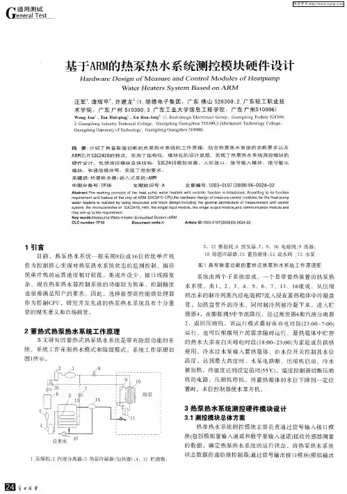
Hardware manualBCU-02/12/22 control unitsList of related manualsYou can find manuals and other product documents in PDF format on the Internet. See section Document library on the Internet on the inside of the back cover. For manuals not available in the Document library, contact your local ABB representative.General manualsCode (English)Safety instructions for ACS880 multidrive cabinets and modules3AUA0000102301Electrical planning instructions for ACS880 multidrive cabinets and modules3AUA0000102324Cabinet design and construction instructions for ACS880 multidrive modules3AUA0000107668BCU-02/12/22 control units hardware manual 3AUA0000113605Supply module manualsACS880-204 IGBT supply modules hardware manual 3AUA0000131525ACS880 IGBT supply control program firmware manual3AUA0000131562ACS880-304 +A018 diode supply modules hardware manual 3AXD50000010104ACS880 diode supply control program firmware manual3AUA0000103295ACS880-904 regenerative rectifier modules hardware manual 3AXD50000020457ACS880 regenerative rectifier control program firmware manual3AXD50000020827Inverter module manualsACS880-104 inverter modules hardware manual 3AUA0000104271ACS880 primary control program firmware manual 3AUA0000085967ACS880 primary control program quick start-up guide 3AUA0000098062Manuals for application programs (Crane, Winder, etc.)Brake module and DC/DC converter module manuals ACS880-604 3-phase brake chopper modules hardware manual3AXD50000022033ACS880 brake control program firmware manual (3-phase brake)3AXD50000020967ACS880-1604 DC/DC converter modules hardware manual 3AXD50000023642ACS880 DC/DC converter control program firmware manual 3AXD50000024671Module package hardware manualsACS880-04 module packages hardware manual3AUA0000138495ACS880-04XT drive modules (500 to 1200 kW) hardware manual3AXD50000025169ACS880-14 and -34 module packages hardware manual 3AXD50000022021Option manualsFSO-12 safety functions module user's manual3AXD50000015612FDPI-02 diagnostics and panel interface user’s manual3AUA00001136183AUA0000113605 Rev CENEFFECTIVE: 2015-05-292015 ABB Oy. All Rights Reserved.3 Table of contents1. BCU-02/12/22 control unitsContents of the manual . . . . . . . . . . . . . . . . . . . . . . . . . . . . . . . . . . . . . . . . . . . . . . . . . . . 5 Safety . . . . . . . . . . . . . . . . . . . . . . . . . . . . . . . . . . . . . . . . . . . . . . . . . . . . . . . . . . . . . . . . 5 Terms and abbreviations . . . . . . . . . . . . . . . . . . . . . . . . . . . . . . . . . . . . . . . . . . . . . . . . . . 5 Hardware description . . . . . . . . . . . . . . . . . . . . . . . . . . . . . . . . . . . . . . . . . . . . . . . . . . . . 6 Fiber optic connections . . . . . . . . . . . . . . . . . . . . . . . . . . . . . . . . . . . . . . . . . . . . . . . . . 7 Layout . . . . . . . . . . . . . . . . . . . . . . . . . . . . . . . . . . . . . . . . . . . . . . . . . . . . . . . . . . . . . . 7 The 7-segment display . . . . . . . . . . . . . . . . . . . . . . . . . . . . . . . . . . . . . . . . . . . . . . . . 11 Checking the delivery . . . . . . . . . . . . . . . . . . . . . . . . . . . . . . . . . . . . . . . . . . . . . . . . . . . 11 Identifying different control unit types . . . . . . . . . . . . . . . . . . . . . . . . . . . . . . . . . . . . . 11 Mechanical installation . . . . . . . . . . . . . . . . . . . . . . . . . . . . . . . . . . . . . . . . . . . . . . . . . . 12Installing the control unit . . . . . . . . . . . . . . . . . . . . . . . . . . . . . . . . . . . . . . . . . . . . . . . 13 Vertical DIN rail mounting . . . . . . . . . . . . . . . . . . . . . . . . . . . . . . . . . . . . . . . . . . . 13 Horizontal DIN rail mounting . . . . . . . . . . . . . . . . . . . . . . . . . . . . . . . . . . . . . . . . . 14 Installing the FSO-xx safety functions module . . . . . . . . . . . . . . . . . . . . . . . . . . . . . . 15 Electrical installation . . . . . . . . . . . . . . . . . . . . . . . . . . . . . . . . . . . . . . . . . . . . . . . . . . . . 16 Fault tracing . . . . . . . . . . . . . . . . . . . . . . . . . . . . . . . . . . . . . . . . . . . . . . . . . . . . . . . . . . 16 LEDs . . . . . . . . . . . . . . . . . . . . . . . . . . . . . . . . . . . . . . . . . . . . . . . . . . . . . . . . . . . . . . 16 Maintenance . . . . . . . . . . . . . . . . . . . . . . . . . . . . . . . . . . . . . . . . . . . . . . . . . . . . . . . . . . 17 Replacing the real-time clock battery . . . . . . . . . . . . . . . . . . . . . . . . . . . . . . . . . . . . . 17 Replacing the memory unit . . . . . . . . . . . . . . . . . . . . . . . . . . . . . . . . . . . . . . . . . . . . . 17 Replacing the SD/SDHC memory card . . . . . . . . . . . . . . . . . . . . . . . . . . . . . . . . . . . 17 Replacing the control unit . . . . . . . . . . . . . . . . . . . . . . . . . . . . . . . . . . . . . . . . . . . . . . 17 Replacement illustration . . . . . . . . . . . . . . . . . . . . . . . . . . . . . . . . . . . . . . . . . . . . . . . 18 Technical data . . . . . . . . . . . . . . . . . . . . . . . . . . . . . . . . . . . . . . . . . . . . . . . . . . . . . . . . . 19 Connector data . . . . . . . . . . . . . . . . . . . . . . . . . . . . . . . . . . . . . . . . . . . . . . . . . . . 19 Ground isolation diagram . . . . . . . . . . . . . . . . . . . . . . . . . . . . . . . . . . . . . . . . . . . . 21 Dimensions . . . . . . . . . . . . . . . . . . . . . . . . . . . . . . . . . . . . . . . . . . . . . . . . . . . . . . 22 Battery . . . . . . . . . . . . . . . . . . . . . . . . . . . . . . . . . . . . . . . . . . . . . . . . . . . . . . . . . . 22 Protection classes . . . . . . . . . . . . . . . . . . . . . . . . . . . . . . . . . . . . . . . . . . . . . . . . . 22 Ambient conditions . . . . . . . . . . . . . . . . . . . . . . . . . . . . . . . . . . . . . . . . . . . . . . . . . 22 Materials . . . . . . . . . . . . . . . . . . . . . . . . . . . . . . . . . . . . . . . . . . . . . . . . . . . . . . . . 22 Applicable standards . . . . . . . . . . . . . . . . . . . . . . . . . . . . . . . . . . . . . . . . . . . . . . . 22 Markings . . . . . . . . . . . . . . . . . . . . . . . . . . . . . . . . . . . . . . . . . . . . . . . . . . . . . . . . 22 Cyber security disclaimer . . . . . . . . . . . . . . . . . . . . . . . . . . . . . . . . . . . . . . . . . . . . . . . . 22 Dimension drawing . . . . . . . . . . . . . . . . . . . . . . . . . . . . . . . . . . . . . . . . . . . . . . . . . . . . . 23 Further informationProduct and service inquiries . . . . . . . . . . . . . . . . . . . . . . . . . . . . . . . . . . . . . . . . . . . . . 25 Product training . . . . . . . . . . . . . . . . . . . . . . . . . . . . . . . . . . . . . . . . . . . . . . . . . . . . . . . . 25 Providing feedback on ABB Drives manuals . . . . . . . . . . . . . . . . . . . . . . . . . . . . . . . . . . 25 Document library on the Internet . . . . . . . . . . . . . . . . . . . . . . . . . . . . . . . . . . . . . . . . . . . 254BCU-02/12/22 control units 5 BCU-02/12/22 control unitsContents of the manualThis manual contains a description of the use and structure of the control unit and its technical data. It also describes how to install and maintain the control unit.For safety information, see Safety instructions for ACS880 multidrive cabinets and modules (3AUA0000102301 [English]) or ACS880-04XT drive modules (500 to 1200 kW) hardware manual (3AXD50000025169 [English]).For information on the unit’s electrical installation, see Electrical planning instructions for ACS880 multidrive cabinets and modules (3AUA0000102324 [English]) and the appropriate drive/converter/inverter hardware manual or ACS880-04XT drive modules (500 to 1200 kW) hardware manual (3AXD50000025169 [English]).For information on the electrical installation of the FSO-xx safety functions module, see the FSO safety functions module user's manual.For the default I/O connection diagrams and more information on the connections, see the appropriate drive/converter/inverter hardware manual.For the related manuals, see List of related manuals.SafetyWARNING! Obey the safety instructions in Safety instructions for ACS880multidrive cabinets and modules (3AUA0000102301 [English]) or ACS880-04XTdrive modules (500 to 1200 kW) hardware manual (3AXD50000025169 [English]). If you ignore them, injury or death, or damage to the equipment can occur.Terms and abbreviationsLater in this manual, term converter substitutes for string drive/converter/inverter.6 BCU-02/12/22 control unitsHardware descriptionThe BCU-02, BCU-12 and BCU-22 are control units used for controlling converters via fiber optic links. It contains integrated branching unit functionality for collecting and storing real-time data from the converter modules to help fault tracing and analysis. The data is stored in a secure data card.The control unit types have a different number of fiber optic connections:BCU type No. of fiber optic connections Can be replaced withBCU-022BCU-02, BCU-12, BCU-22BCU-127BCU-12, BCU-22BCU-2212BCU-22You can use a BCU-22 to replace any of the control unit types.The control unit requires an external 24V DC power source. It has three option slots for I/O extensions, encoders and fieldbus adapters, an integrated Ethernet port for PC tool communication and a removable memory unit. For example, if the control unit needs to be replaced, the parameter settings can be retained by transferring the memory unit from the defective control unit to the new one.The control unit has an on-board data logger that collects real-time data from the converter power stages to help fault tracing and analysis. The data is stored onto the SDHC memory card inserted into the SD CARD slot and can be analyzed by ABB service personnel.The drive-to-drive link (XD2D) is a daisy-chained RS-485 transmission line that allows basic master/follower communication with one master and multiple followers. The control unit has also one option slot for connecting the RDCO DDCS communication option board. For more information, see the appropriate hardware manual.BCU-02/12/22 control units 7⏹Fiber optic connectionsThe BCU-02 control unit has two fiber optic connections V1and V2 for connecting to converter modules. The control unit does not include the BPEB-05 board. The BCU-12 control unit includes one BPEB-05 board that adds five connections to it (V3…V7), while the BCU-22 control unit includes two BPEB-05 boards and thus twelve connections (V1…V12).For instructions on connecting the control unit to the converter module, see theappropriate hardware manual .⏹LayoutThe following figures show the layout of the BCU-22 control unit. For the default I/O connection diagrams and more information on the connections, see the appropriate hardware manual.V1V2 V3V4 V5 V 6V7V8 V9 V10 V11 V12xINT Module 1xINT Module 3I/OBPEB-05BCU-x2BIOC-01BPEB-05xINT Module 2xINT Module 7xINT Module 8xINT Module 128 BCU-02/12/22 control units10 BCU-02/12/22 control unitsDescriptionI/O connectorXAI Analog inputXAO Analog outputXDI Digital input and digital start interlockXDIO Digital input/outputXD2D Drive-to-drive linkXD24+24 V output for digital inputXPOW External power inputXRO1Relay output 1XRO2Relay output 2XRO3Relay output 3XSTO Safe torque off connection (input signal).Note: This input only acts as a true Safe torque off input in control units controlling a motor.In other applications (such as a supply or brake unit), de-energizing the IN1 and/or IN2terminal will stop the unit but does not constitute a true safety function.For more information on Safe torque off, see the appropriate hardware manual.XSTO OUT Safe torque off connection (output for powering XSTO input of inverter modules).X485Not in useSwitchAI1Analog input 1 current/voltage selectionAI2Analog input 2 current/voltage selectionD2D TERM Drive-to-drive link terminationDICOM = DIOGND Determines whether DICOM is separated from DIOGND (ie, common reference for digital inputs floats).Fiber optic connectorV1T…V12T,V1R…V12RFiber optic connector to converter module: T = Transmitter, R = ReceiverConnector for optional moduleSLOT 1F-type adapter, interface and I/O extension modulesIf FDPI-02 diagnostics and panel interface is used, it has to be installed in slot 1 with twoscrews.SLOT 2F-type adapter, interface and I/O extension modulesSLOT 3F-type adapter, interface and I/O extension modules, FSO-xx safety functions module SLOT 4RDCO-0x DDCS communication option modulesSafety option connectorX12Cable connector for the FSO-xx safety functions module.Note: The FSO-xx safety functions module can be used only with ACS880 inverters.For more information on the FSO-xx safety functions module, see the FSO safety functionsmodule user's manual.Control panel and Ethernet connectorXETH Ethernet port for, eg, PC communicationX13Control panelMemory unit and card connectorX205MEMORYUNITConverter memory unit connectorSD CARD Secure digital card holder (Data logger memory for the fiber optic links)DescriptionMiscellaneous+ Battery Real-time clock battery⏹The 7-segment displayThe following table describes the indications of the 7-segment display on the control unit. Multicharacter indications are displayed as repeated sequences of characters.“U” is indicated shortly before “o”.The control program has been launched and is running.Flashing character.The firmware cannot be started: The memory unit is missing or corrupted.The firmware download from a PC to the control unit is in progress.At the converter power-up, the 7-segment display can show short indications of, for example,“1”, “2”, “b” or “U”. These are normal indications immediately after powering up the converter.If the 7-segment display ends up showing other values than described above after thepower-up, it indicates a hardware failure.Checking the deliveryCheck that all items listed below are present. Check that there are no signs of damage:•control unit with the I/O connectors•memory unit•SD/SDHC flash memory card (inserted in its slot)•real-time clock battery.⏹Identifying different control unit typesBefore installation, check that the control unit has the correct control program for the converter hardware in question. The control program is shown in the label attached to the memory unit.Check also that the control unit is suitable for your equipment configuration.Mechanical installationWARNING! Do not install the control unit in the immediate vicinity ofelectromagnetic disturbance sources, such as relays, contactors, brake choppers, power and motor cabling. The minimum recommended distance from such components is 200mm. We recommend to install metallic screening between the control unit and the source of disturbance. This can reduce the required distance.WARNING! Mount the control unit so that air can pass freely through theventilation holes in the housing. Avoid mounting directly above heat-generatingequipment.You can mount the control unit on a vertical or horizontal standard 35×7.5/15 mm DIN rail. In vertical direction, you can mount the unit either top or bottom upwards. When mounting the unit horizontally, the connectors must be downwards and the connector texts the right way up.Leave enough space for cabling, and replacing the memory unit and real-time clock battery. See sections Replacing the real-time clock battery, Replacing the memory unit and Replacing the SD/SDHC memory card on page 17.Installing the control unitThe control unit is grounded through the DIN rail.Vertical DIN rail mounting1.Fasten the latch to the back of the control unit with four screws.2.Click the control unit to the rail as shown below.3.Secure the control unit with an end bracket.Horizontal DIN rail mounting1.Fasten the latches to the back of the control unit with four screws.2.Click the control unit to the rail as shown below.Installing the FSO-xx safety functions module1.Fasten the FSO-xx safety functions module onto slot3 with four screws.2.Tighten the FSO-xx electronics grounding screw (0.8 N·m).3.Connect the FSO-xx data cable to FSO-xx connector X110 and to BCU-x2 connectorX12.For information on the electrical installation of the FSO-xx safety functions module, see the FSO safety functions module user's manual.Electrical installationWARNING! Obey the safety instructions given in Safety instructions for ACS880multidrive cabinets and modules [3AUA0000102301 (English)] or ACS880-04XTdrive modules (500 to 1200 kW) hardware manual (3AXD50000025169 [English]).If you ignore the safety instructions, injury or death can occur. If you are not aqualified electrician, do not do electrical work.Connect the +24V external power supply to the control unit connector XPOW.Connect the fiber optic cables and gate driver board wiring from the converter module to the control unit according to the instructions given in the converter module hardware manual.For general electrical installation instructions, see Electrical planning instructions for ACS880 multidrive cabinets and modules [3AUA0000102324 (English)] or ACS880-04XT drive modules (500 to 1200 kW) hardware manual (3AXD50000025169 [English]). Fault tracingLEDsLEDBATT OK When lit, the battery voltage of the real time clock is OK (higher than 2.8V).When off,•battery voltage is below 2.8V,•battery is missing, or•control unit is not powered.PWR OK When lit, internal voltage is OK.FAULT When lit, the control program indicates that the equipment is faulty. See the appropriate firmware manual.WRITE When lit, writing to the SD card is in progress.Maintenance⏹Replacing the real-time clock batteryReplace the real-time clock battery if the BATT LED is not illuminated when the control unit is powered. For information on the LED, see Fault tracing on page 16.See A in figure Replacement illustration on page 18.1.Undo the fastening screw and remove the battery. For the replacement battery type,see Real-time clock battery on page 22.2.Insert the new battery according to figure Replacement illustration.3.Dispose the old battery according to local disposal rules or applicable laws.4.Set the real-time clock.⏹Replacing the memory unitSee B in figure Replacement illustration on page 18.1.To remove the memory unit, undo the fastening screw and pull the memory unit out.See the following figure.2.Insert the new memory unit and fasten the screw.⏹Replacing the SD/SDHC memory cardNote: Do not remove the SD card while the yellow WRITE LED is lit. Writing to the SD card is in progress.See C in figure Replacement illustration on page 18.1.Undo the fastening screw of the clip covering the memory card and press the card toremove it. For the card location, see the following figure. For the replacement card type, see Ground isolation diagram on page 21.2.Insert the new card in reverse order.⏹Replacing the control unitSee section Installing the control unit on page 13.1.If the control unit has been installed vertically, remove the end bracket.2.Remove the control unit from the rail.3.Undo the four fastening screws with which the latch has been fastened to the back ofthe control unit.4.Pull out the detachable terminal blocks which have control cables connected.5.Install the new control unit in reverse order.Note: If there is a safety circuit connected to the STO terminals (XSTO) of the control unit, redo its acceptance test according to the instructions given in the inverter or drive module hardware manual.See the appropriate documentation: drive or inverter module hardware manual, safety option user’s manual and/or FSO safety functions module user’s manual.Replacement illustrationTechnical data Connector dataPower supply (XPOW)Connector pitch 5mm, wire size 2.5mm224V(±10%)DC, 2AExternal power input. Two supplies can be connected for redundancy.Relay outputs RO1…RO3 (XRO1…XRO3)Connector pitch 5 mm, wire size 2.5mm2 250V AC / 30V DC, 2AProtected by varistors+24 V output(XD24:2 and XD24:4)Connector pitch 5mm, wire size 2.5mm2Total load capacity of these outputs is 4.8W (200mA / 24V) minus the power taken by DIO1 and DIO2.Digital inputs DI1…DI6 (XDI:1…XDI:6)Connector pitch 5mm, wire size 2.5mm224V logic levels: “0”< 5V, “1”>15VR in: 2.0kohmInput type: NPN/PNP (DI1…DI5), NPN (DI6)Hardware filtering: 0.04ms, digital filtering up to 8msDI6 (XDI:6) can alternatively be used as an input for a PTC thermistor.“0” >4kohm, “1”<1.5kohmI max: 15mA (DI1…DI5), 5mA (DI6)Start interlock input DIIL (XDI:7)Connector pitch 5mm, wire size 2.5mm224V logic levels: “0”< 5V, “1” >15VR in: 2.0kohmInput type: NPN/PNPHardware filtering: 0.04ms, digital filtering up to 8 msDigital inputs/outputs DIO1 and DIO2(XDIO:1…XDIO:4)Input/output mode selection by parameters. DIO1 can be configured as a frequency input (0…16 kHz with hardware filtering of 4 microseconds) for 24 V level square wave signal (sinusoidal or other wave form cannot be used). DIO2 can be configured as a 24V level square wave frequency output. See the firmware manual.Connector pitch 5mm, wire size 2.5mm2As inputs:24V logic levels: “0” <5V, “1” >15VR in: 2.0kohmFiltering: 1msAs outputs:Total output current from +24VD is limited to 200mAReference voltage for analog inputs +VREF and -VREF(XAI:1 and XAI:2)Connector pitch 5mm, wire size 2.5mm210V ±1% and –10V ±1%, R load 1…10kohm Maximum output current: 10 mAR LDIOxDIOGND+24VDAnalog inputs AI1 and AI2 (XAI:4 … XAI:7).Current/voltage input mode selection by switches Connector pitch 5mm, wire size 2.5mm2Current input: –20…20mA, R in: 100ohmVoltage input: –10…10 V, R in > 200kohmDifferential inputs, common mode range ±30VSampling interval per channel: 0.25msHardware filtering: 0.25ms, adjustable digital filtering up to 8ms Resolution: 11 bit + sign bitInaccuracy: 1% of full scale rangeInaccuracy with Pt100 sensors: 10 °C (50 °F)Analog outputs AO1 and AO2(XAO)Connector pitch 5 mm, wire size 2.5mm2 0…20mA, R load < 500ohmFrequency range: 0…500Hz Resolution: 11 bit + sign bit Inaccuracy: 2% of full scale rangeDrive-to-drive link (XD2D)Connector pitch 5mm, wire size 2.5mm2 Physical layer: RS-485Termination by switchRS-485 connection (X485)Connector pitch 5mm, wire size 2.5mm2 Physical layer: RS-485Safe torque off connection (XSTO)Connector pitch 5mm, wire size 2.5mm2Input voltage range: -3…30V DCLogic levels: “0” < 5V, “1” >17VFor the unit to start, both connections must be “1”Current consumption: 66 mA (continuous) per STO channel per inverter moduleEMC (immunity) according to IEC61326-3-1Safe torque off output (XSTO OUT)Connector pitch 5mm, wire size 2.5mm2 To STO connector of inverter moduleControl panel connection (X13)Connector: RJ-45 Cable length < 3mEthernet connection(XETH)Connector: RJ-45SDHC memory card slot (SD CARD)Memory card type: SDHC Maximum memory size: 4GBThe terminals on the board fulfil the Protective Extra Low Voltage (PELV) requirements. The PELV requirements of a relay output are not fulfilled if a voltage higher than 48 V is connected to the relay output.BCU-02/12/22 control units 21 Ground isolation diagramXPOW+24VI1GND2+24VI3GND4XAI+VREF1-VREF2AGND3AI1+4AI1-5AI2+6AI2-7XAOAO11AGND2AO23AGND4XD2DB1A2BGND3SHIELD4XRO1, XRO2, XRO3NC11COM12NO13NC21COM22NO23NC31COM32NO33XD24+24VD5DICOM6+24VD7DIOGND8XDIODIO11DIO22DIOGND3DIOGND4XDI DI11DI22DI33DI44DI55DI66 DIIL7XSTO OUT1 SGND2IN13IN24XSTO OUT IN15 SGND6IN27 SGND8*Ground Common mode voltage betweeneach AI input and AGND is+30V*Ground selector (DICOM=DIOGND) settingsDICOM=DIOGND: ONAll digital inputs share a common ground (DICOM connected to DIOGND). This is the default setting.DICOM=DIOGND: OFFGround of digital inputs DI1…DI5 and DIIL (DICOM) is isolated from DIO signal ground (DIOGND). Isolation voltage 50 V.22 BCU-02/12/22 control unitsDimensionsCyber security disclaimerThis product is designed to be connected to and to communicate information and data via a network interface. It is Customer's sole responsibility to provide and continuously ensure a secure connection between the product and Customer network or any other network (as the case may be). Customer shall establish and maintain any appropriate measures (such as but not limited to the installation of firewalls, application of authentication measures, encryption of data, installation of anti-virus programs, etc) to protect the product, thenetwork, its system and the interface against any kind of security breaches, unauthorized access, interference, intrusion, leakage and/or theft of data or information. ABB and its affiliates are not liable for damages and/or losses related to such security breaches, any unauthorized access, interference, intrusion, leakage and/or theft of data or information.Height Width Width with connectors Depth Depth with memory unit Depth with memory unit and latch mm in mm in mm in mmin mm in mm in 31112.241254.921395.4774 2.91104.331154.53BatteryReal-time clock batteryBR2032Protection classesDegree of protection (IEC/EN 60529)IP10Enclosure type (UL 508C)UL Open Type Overvoltage category (IEC 60664-1)II Protective class (IEC/EN 61800-5-1)I Protective class (IEC 62109-1)IIAmbient conditionsAir temperature in operation+0 to +70 °C (158 °F)MaterialsHousing Hot-dip zinc coated steel, cover painted PackageCardboardApplicable standardsEN 61800-5-1:2007Adjustable speed electrical power drive systems. Part 5-1: Safety requirements – electrical, thermal and energyEN 61800-3:2004Adjustable speed electrical power drive systems. Part 3: EMC requirements and specific test methodsIEC/EN 62109-1:2010Safety of power converters for use in photovoltaic power systems Part 1: General requirementsUL508C:2002UL Standard for Safety, Power Conversion Equipment, third editionNote: For other standards, see the appropriate hardware and functional safety manuals.MarkingscULusThe control unit is cULus Listed.24 BCU-02/12/22 control unitsFurther informationProduct and service inquiriesAddress any inquiries about the product to your local ABB representative, quoting the type designation and serial number of the unit in question. A listing of ABB sales, support and service contacts can be found by navigating to /searchchannels.Product trainingFor information on ABB product training, navigate to /drives and select ABB University.Providing feedback on ABB Drives manualsYour comments on our manuals are welcome. Go to /drives and select Document Library – Manuals feedback form (LV AC drives).Document library on the InternetYou can find manuals and other product documents in PDF format on the Internet at /drives/documents.。
硬件单元模块设计
正负24V电源为电流变送器供电,正3..3V为MSP430单片机供电,5V为其他器件供电。
该电源主要通过整流、滤波和稳压三部分构成,部分功能如下:
桥式整流电路:
图3.1.1(a)整流电路
电容滤波电路的特点:
(1)电流的有效值和平均值的关系与波形有关,在平均值相同的情况下,波形越尖,有效值越大。在纯电阻负载时,变压器副
边的有效值I2=1.11IL,而有电容滤波时I2=(1.5~2)IL。
(2)负载平均电压VL升高,纹波(交流成分)减小,且RLC越大,电容放电速率越慢,则负载电压中的纹波成分越小,负载平
均电压越高。为了得到平滑的负载电压,一般取RL*C≥(3~5)T/2(式中T为电源交流电压的周期)。
(3)负载直流电压随负载电流增加而减小。VL随IL的变化关系称为输出特性或外特性。
电容滤波电路简单,负载直流电压VL较高,纹波也较小,它的缺点是输出特性较差,适用于负载电压较高,负载变动不大的场
合。
一、 方案比较、设计与论证
1.1正弦信号发生器的设计方案论证与选择
1.2二线式电流变送器
的设计方案论证与选择:
方案一:采用专门集成电流变送器芯片XTR115如图(1),它属于二线制电流变
送器,内部的2.5V基准电压可作为传感器的激励源,它能将输入电压转换成4~
20mA的电流信号,其输出电压精度为±0.05%,电压温度系数仅为20×10-6/℃,
可给外部电路(例如前置放大器)单独供电,从而简化了外部电源的设计.精度
高,非线性误差小。转换精度可达±0.05%,非线性误差仅为±0.003%
。
图(1)
方案2
采用lm358搭建电流的发送和接收部分的电路,lm358静态偏置电流小,且为单电源供电,即使在没有负电源情况下,
输入端仍能够接受0V输入并能正常工作。相比方案一成本比上减少10倍以上.,更适合实际应用。同时题目明确要求不
能采用专用变送器或电流转换器芯片,所以我们选择方案二。
电流放送
电流接收
二线式电流变送
1.3滤波放大电路
滤波电路
放大电路
方案一:采用无输出电容功率放大电路(OCL电路)。采用两只MOSFET配对场效应管组成OCL低频功率放大电路可以实
现对正弦信号的放大,匹配负载电阻,使匹配负载的电压峰峰值Vopp≥5V,能实现题目要求。但OCL电路相对BUF634
构成的功率放大电路复杂。
方案二;
滤波电路采用OPA404二阶有源滤波,放大电路采用 AD828。在实际测试中这个电路能有效滤出1000kHz到2000kHz的
正弦波中的杂波,而且放大部分能使输出峰峰值能达到6V以上,完全能达到题目要求。
1.2正弦信号发生器的设计方案论证与选择
二.
理论分析与计算
2.1电流变送器的原理分析;
两线制变送器的结构与原理两线制变送器的原理是利用了4~20mA信号为自身提供电能。如果变送器自身耗电大于4mA,
那么将不可能输出下限4mA值。因此一般要求两线制变送器自身耗电(包括传感器在内的全部电路)不大于3.5mA。这
是两线制变送器的设计根本原则之一。从整体结构上来看,两线制变送器由三大部分组成:传感器、调理电路、两线制
V/I变换器构成。传感器将温度、压力等物理量转化为电参量,调理电路将传感器输出的微弱或非线性的电信号进行放大、
调理、转化为线性的电压输出。两线制V/I变换电路根据信号调理电路的输出控制总体耗电电流;同时从环路上获得电
压并稳压,供调理电路和传感器使用。除了V/I变换电路之外,电路中每个部分都有其自身的耗电电流,两线制变送器
的核心设计思想是将所有的电流都包括在V/I变换的反馈环路内。两线制V/I变换器 V/I 变换器是一种可以用电压信号
控制输出电流的电路。两线制V/I变换器与一般V/I变换电路不同点在:电压信号不是直接控制输出电流,而是控制整个
电路自身耗电电流。同时,还要从电流环路上提取稳定的电压为调理电路和传感器供电.
2.2 测量精度分析;
1.测量精度按贝塞尔公式计算;
2.非线性度计算公式为:非线性度=[最大误差(满度-零度)]100%;
3系统测试
3.1测试仪器
3.1.1测试示波器介绍
DS1000E示波器是一款高性能指标、经济型的数字示波器,广泛应用于教育培训、产线测试和企业科研等各个领域。
产品特性
1. 提供2个模拟通道,最高100MHz带宽,1 GSa/s实时采样率及25GSa/s等效采样率;
2. 5.6英寸QVGA(320×240),64k色TFT彩色液晶显示屏
3. 1Mpts存储深度
4. 边沿、脉宽、斜率、视频、交替触发功能
3.2;TH2818型自动元件分析仪
TH2818型自动元件分析仪是一种精度高、测试范围宽、6位测试分辨率的阻抗测量仪器,高达300kHz的测试频率,以0.01Hz
步进任意编程、5mV~2V信号电平及直流内偏置电压, 并能提供变压器测试能力及元件频率响应分析能力,可满足生产
线质量保证、进货检验及实验室高精确度测量要求。仪器所提供的HANDLER、GPIB、RS232C接口为仪器使用于元件自动
分选系统、与计算机通讯及测试过程记录提供了条件。
数据测试、、
数据测试
通过键盘选择,得到数据如下表:
表6.2.2部分测试数据
设定电阻() 显示电阻() 显示频率(kHz) 测得频率(kHz)
1000 1003 1002.8 1002.5
1250 1249 1248.5 1249.0
1500 1499 1499.9 1499.8
1800 1797 1796.8 1795.5
2000 1996 1993.9 1990.7
把输出端接上50的负载电阻,从数字示波器上读出Vopp =5.95V,基本达到设计要求。示波器的波形较平滑,无明显失
真。
根据贝塞尔公式计算:
1000时为0
1250时为2
1500时为0.5
1800时为0.5
2000时为2
根据非线性度计算公式为:非线性度=[最大误差(满度-零度)]100%
非线性度为=-0.4%
从表和上面计算可以看出,系统基本上稳定但还有待继续提高精度。
4设计总结
通过几天的共同努力我们完成了受控正弦信号发生器的设计。通过键盘选择后。当电阻箱电阻变化经过电流传送和接收
部分后提供给单片机处理。当电阻大于1500Ω输出固定频率1000kHz,当小于1500Ω时波形发生器停止工作。经过测试
功能能基本完成。当电阻在1000Ω和2000Ω之间变化时输出正弦波频率能跟随电阻在1000kHz到2000kHz内变化。在波
形输出端加了我们设计的滤波和放大电路能有效排除干扰,使波形无明显失真,在50负载电阻上的电压峰峰值Vopp≥
5V 。最后我们还对部分的功能进行了改进,当电阻大于1500Ω默认输出固定频率为1000kHz,我们还可以用键盘设定
输出固定频率的值。