MAX6364HUT23中文资料
- 格式:pdf
- 大小:178.53 KB
- 文档页数:12

For free samples & the latest literature: , or phone 1-800-998-8800.For small orders, phone 1-800-835-8769.General DescriptionThe MAX6326/MAX6327/MAX6328/MAX6346/MAX6347/MAX6348 microprocessor (µP) supervisory circuits moni-tor the power supplies in µP and digital systems. These devices provide excellent circuit reliability and low cost by eliminating external components and adjustments when used with 2.5V, 3V, 3.3V, and 5V powered circuits.These circuits perform a single function: they assert a reset signal whenever the V CC supply voltage declines below a preset threshold, keeping it asserted for at least 100ms after V CC has risen above the reset threshold.The only difference between the devices is their output.The MAX6326/MAX6346 (push-pull) and MAX6328/MAX6348 (open-drain) have an active-low reset output.The MAX6327/MAX6347 have an active-high push-pull reset output. All of these parts are guaranteed to be in the correct state for V CC down to 1V. The reset compara-tor is designed to ignore fast transients on V CC . Reset thresholds are factory-trimmable between 2.2V and 4.63V, in approximately 100mV increments. Twenty-one standard versions are available. Contact the factory for availability of nonstandard versions.Ultra-low supply currents (1µA max for the MAX6326/MAX6327/MAX6328) make these parts ideal for use in portable equipment. All six devices are available in space-saving SOT23 and SC70 packages.ApplicationsComputers Intelligent Instruments Controllers AutomotiveCritical µP and µC Portable/Battery-Powered Power MonitoringEquipmentFeatureso Ultra-Low 1µA (max) Supply Current (MAX6326/MAX6327/MAX6328)o Precision Monitoring of 2.5V, 3V, 3.3V, and 5V Power-Supply Voltageso Reset Thresholds Available from 2.2V to 4.63V o Fully Specified Over Temperatureo 100ms (min) Power-On Reset Pulse Width o Low Costo Available in Three Versions: Push-Pull RESET ,Push-Pull RESET, and Open-Drain RESET o Power-Supply Transient Immunity o No External Componentso 3-Pin SC70/SOT23 Packageso Pin Compatible with MAX803/MAX809/MAX810MAX6326/MAX6327/MAX6328/MAX6346/MAX6347/MAX63483-Pin, Ultra-Low-Power SC70/SOTµP Reset Circuits________________________________________________________________Maxim Integrated Products 1Pin Configuration19-1294; Rev 3; 1/00†The MAX6326/MAX6327/MAX6328/MAX6346/MAX6347/MAX6348 are available in factory-set V CC reset thresholds from 2.2V to 4.63V, in approximately 0.1V increments. Choose the desired reset-threshold suffix from Table 1 and insert it in the blank spaces following “R.”There are 21 standard versions witha required order increment of 2500 pieces. Sample stock is gen-erally held on the standard versions only (see the SelectorGuide). Required order increment is 10,000 pieces for nonstan-dard versions (Table 2). Contact factory for availability. All devices available in tape-and-reel only.Selector Guide appears at end of data sheet.M A X 6326/M A X 6327/M A X 6328/M A X 6346/M A X 6347/M A X 63483-Pin, Ultra-Low-Power SC70/SOT µP Reset Circuits 2_______________________________________________________________________________________ABSOLUTE MAXIMUM RATINGSELECTRICAL CHARACTERISTICS(V CC = full range, T A = -40°C to +85°C, unless otherwise noted. Typical values are at T A = +25°C and V CC = 3V.) (Note 1)Stresses beyond those listed under “Absolute Maximum Ratings” may cause permanent damage to the device. These are stress ratings only, and functional operation of the device at these or any other conditions beyond those indicated in the operational sections of the specifications is not implied. Exposure to absolute maximum rating conditions for extended periods may affect device reliability.Terminal Voltage (with respect to GND)V CC ...........................................................................-0.3V to +6V RESET, RESET (push-pull).........................-0.3V to (V CC + 0.3V)RESET (open drain)..................................................-0.3V to +6V Input Current (V CC ).............................................................20mA Output Current (RESET, RESET ).........................................20mA Rate of Rise (V CC )...........................................................100V/µsContinuous Power Dissipation (T A = +70°C)3-Pin SC70 (derate 2.7mW/°C above +70°C)...............174mW 3-Pin SOT23 (derate 4mW/°C above +70°C)................320mW Operating Temperature Range ...........................-40°C to +85°C Storage Temperature Range.............................-65°C to +150°C Lead Temperature (soldering, 10s).................................+300°CNote 1:Overtemperature limits are guaranteed by design and not production tested.MAX6326/MAX6327/MAX6328/MAX6346/MAX6347/MAX63483-Pin, Ultra-Low-Power SC70/SOTµP Reset Circuits_______________________________________________________________________________________3__________________________________________Typical Operating Characteristics(T A = +25°C, unless otherwise noted.)00.30.20.10.40.50.60.70.80.91.0-400-2020406080SUPPLY CURRENT vs. TEMPERATURE TEMPERATURE (°C)S U P P L Y C U R R E N T(µA)050100150200-400-2020406080POWER-DOWN RESET DELAY vs. TEMPERATURE TEMPERATURE (°C)R E S E T D E L A Y(µs)130150140160170180190200210-400-2020406080POWER-UP RESET TIMEOUT vs. TEMPERATURE M A X6326-03TEMPERATURE (°C)P O W E R-U P R E S E T T I M E O U T(m s)500011001000MAXIMUM TRANSIENT DURATION vs. RESET THRESHOLD OVERDRIVE (SC70)100300400200M A X6326-04RESET THRESHOLD OVERDRIVE,V TH - V CC (mV)M A X I M U M T R A N S I E N T D U R A T I O N(µs)10______________________________________________________________Pin DescriptionM A X 6326/M A X 6327/M A X 6328/M A X 6346/M A X 6347/M A X 63483-Pin, Ultra-Low-Power SC70/SOT µP Reset Circuits 4___________________________________________________________________________________________________Applications InformationInterfacing to µPs with Bidirectional Reset PinsSince the RESET output on the MAX6328/MAX6348 is open drain, these devices interface easily with micro-processors (µPs) that have bidirectional reset pins,such as the Motorola 68HC11. Connecting the µP supervisor’s RESET output directly to the microcon-troller’s (µC’s) RESET pin with a single pull-up resistor allows either device to assert reset (Figure 1).Negative-Going V CC TransientsIn addition to issuing a reset to the µP during power-up,power-down, and brownout conditions, these devices are relatively immune to short-duration, negative-going V CC transients (glitches).The Typical Operating Characteristics show the Maxi-mum Transient Duration vs. Reset Threshold Overdrive graph, for which reset pulses are not generated. The graph shows the maximum pulse width that a negative-going V CC transient may typically have when issuing a reset signal. As the amplitude of the transient increas-es, the maximum allowable pulse width decreases.Figure 1. Interfacing to µPs with Bidirectional Reset PinsTable 1. Factory-Trimmed Reset Thresholds ‡‡Factory-trimmed reset thresholds are available in approximately 100mV increments with a 1.5% room-temperature variance.MAX6326/MAX6327/MAX6328/MAX6346/MAX6347/MAX63483-Pin, Ultra-Low-Power SC70/SOTµP Reset Circuits_______________________________________________________________________________________5Table 1. Factory-Trimmed Reset Thresholds‡(continued)‡Factory-trimmed reset thresholds are available in approximately 100mV increments with a 1.5% room-temperature variance.Table 2. Device Marking Codes and Minimum Order IncrementsM A X 6326/M A X 6327/M A X 6328/M A X 6346/M A X 6347/M A X 63483-Pin, Ultra-Low-Power SC70/SOT µP Reset Circuits 6__________________________________________________________________________________________________________Chip InformationTRANSISTOR COUNT: 419Table 2. Device Marking Codes and Minimum Order Increments (continued)Selector Guide(standard versions*)*Sample stock is generally held on all standard versions.________________________________________________________Package InformationMAX6326/MAX6327/MAX6328/MAX6346/MAX6347/MAX63483-Pin, Ultra-Low-Power SC70/SOTµP Reset Circuits_______________________________________________________________________________________7M A X 6326/M A X 6327/M A X 6328/M A X 6346/M A X 6347/M A X 63483-Pin, Ultra-Low-Power SC70/SOT µP Reset Circuits Maxim cannot assume responsibility for use of any circuitry other than circuitry entirely embodied in a Maxim product. No circuit patent licenses are implied. Maxim reserves the right to change the circuitry and specifications without notice at any time.8_____________________Maxim Integrated Products, 120 San Gabriel Drive, Sunnyvale, CA 94086 408-737-7600©2000 Maxim Integrated ProductsPrinted USAis a registered trademark of Maxim Integrated Products.Package Information (continued)。


MAX4053CSE+中文资料General DescriptionThe MAX4051/MAX4052/MAX4053 and MAX4051A/MAX4052A/MAX4053A are low-voltage, CMOS analog ICs configured as an 8-channel multiplexer (MAX4051/A),two 4-channel multiplexers (MAX4052/A), and three sin-gle-pole/double-throw (SPDT) switches (MAX4053/A).The A-suffix parts are fully characterized for on-resistance match, on-resistance flatness, and low leakage.These CMOS devices can operate continuously with dual power supplies ranging from ±2.7V to ±8V or a single supply between +2.7V and +16V. Each switch can handle rail-to-rail analog signals. The off-leakage current is only 0.1nA at +25°C or 5nA at +85°C (MAX4051A/MAX4052A/MAX4053A).All digital inputs have 0.8V to 2.4V logic thresholds,ensuring TTL/CMOS-logic compatibility when using ±5V or a single +5V supply.________________________ApplicationsBattery-Operated Equipment Audio and Video Signal Routing Low-Voltage Data-Acquisition Systems Communications Circuits____________________________FeaturesPin Compatible with Industry-Standard74HC4051/74HC4052/74HC4053?Guaranteed On-Resistance:100?with ±5V SuppliesGuaranteed Match Between Channels:6?(MAX4051A–MAX4053A)12?(MAX4051–MAX4053)?Guaranteed Low Off-Leakage Currents:0.1nA at +25°C (MAX4051A–MAX4053A)1nA at +25°C (MAX4051–MAX4053)?Guaranteed Low On-Leakage Currents:0.1nA at +25°C (MAX4051A–MAX4053A)1nA at +25°C (MAX4051–MAX4053)?Single-Supply Operation from +2.0V to +16V Dual-Supply Operation from ±2.7V to ±8V ?TTL/CMOS-Logic Compatible ?Low Distortion: < 0.04% (600?)?Low Crosstalk: < -90dB (50?)?High Off-Isolation: < -90dB (50?)MAX4051/A, MAX4052/A, MAX4053/ALow-Voltage, CMOS AnalogMultiplexers/Switches________________________________________________________________ Maxim Integrated Products1___________________________________PinConfigurations/Functional Diagrams19-0463; Rev 2; 10/05Ordering Information continued at end of data sheet.For pricing, delivery, and ordering information,pleasecontact Maxim/Dallas Direct!at 1-888-629-4642, or visit Maxim’s website at .M A X 4051/A , M A X 4052/A , M A X 4053/ALow-Voltage, CMOS Analog Multiplexers/Switches 2___________________________________________________________________ ____________________ABSOLUTE MAXIMUM RATINGSELECTRICAL CHARACTERISTICS—Dual Supplies(V+ = +4.5V to +5.5V, V- = -4.5V to -5.5V, T A = T MIN to T MAX , unless otherwise noted. Typical values are at T A = +25°C.) Stresses beyond those listed under “Absolute Maximum Ratings” may cause permanent damage to the device. These are stress ratings only, and functional operation of the device at these or any other conditions beyond those indicated in the operational sections of the specifications is not implied. Exposure to absolute maximum rating conditions for extended periods may affect device reliability.Voltages Referenced to GNDV+........................................................................-0.3V to +17V V-..........................................................................+0.3V to -17V V+ toV-................................................................-0.3V to +17V Voltage into Any Terminal (Note 1)..........(V- - 2V) to (V+ + 2V)or 30mA (whichever occurs first)Continuous Current into Any Terminal..............................±30mA Peak Current, NO or COM(pulsed at 1ms, 10% duty cycle).................................±100mAContinuous Power Dissipation (T A = +70°C)Plastic DIP (derate 10.53m W/°C above +70°C)............842mW Narrow SO (derate 8.70mW/°C above +70°C)..............696mW QSOP (derate 8.00mW/°C above +70°C).....................640mW CERDIP (derate 10.00mW/°C above +70°C)................800mW Operating Temperature RangesMAX405_C_ E/MAX405_AC_E.............................0°C to +70°C MAX405_E_ E/MAX405_AE_E...........................-40°C to +85°C MAX405_MJE/MAX405_AMJE........................-55°C to +125°C Storage Temperature Range.............................-65°C to +150°C Lead Temperature (soldering, 10s).................................+300°CNote 1:Signals on any terminal exceeding V+ or V- are clamped by internal diodes. Limit forward-diode current to maximumcurrent rating.ELECTRICAL CHARACTERISTICS—Dual Supplies (continued) MAX4051/A, MAX4052/A, MAX4053/A Low-Voltage, CMOS Analog Multiplexers/Switches(V+ = +4.5V to +5.5V, V- = -4.5V to -5.5V, T A= T MIN to T MAX, unless otherwise noted. Typical values are at T A= +25°C.)M A X 4051/A , M A X 4052/A , M A X 4053/ALow-Voltage, CMOS Analog Multiplexers/Switches 4___________________________________________________________________ ____________________Note 2:The algebraic convention is used in this data sheet; the most negative value is shown in the minimum column.Note 3:?R ON = R ON(MAX)- R ON(MIN).Note 4:Flatness is defined as the difference between the maximum and minimum value of on-resistance as measured over thespecified analog signal ranges; i.e., V NO = 3V to 0V and 0V to -3V.Note 5:Leakage parameters are 100% tested at maximum-rated hot operating temperature, and guaranteed by correlation atT A = +25°C.Note 6:Guaranteed by design, not production tested.ELECTRICAL CHARACTERISTICS—Dual Supplies (continued) (V+ = +4.5V to +5.5V, V- = -4.5V to -5.5V, T A = T MIN to T MAX , unless otherwise noted. Typical values are at T A = +25°C.) ELECTRICAL CHARACTERISTICS—Single +5V SupplyMAX4051/A, MAX4052/A, MAX4053/A Low-Voltage, CMOS Analog Multiplexers/Switches(V+ = +4.5V to +5.5V, V- = 0V, T A= T MIN to T MAX, unless otherwise noted. Typical values are at T A= +25°C.)M A X 4051/A , M A X 4052/A , M A X 4053/ALow-Voltage, CMOS Analog Multiplexers/Switches 6___________________________________________________________________ ____________________ELECTRICAL CHARACTERISTICS—Single +5V Supply (continued)(V+ = +4.5V to +5.5V, V- = 0V, T A = T MIN to T MAX , unless otherwise noted. Typical values are at T A = +25°C.)Note 2:The algebraic convention is used in this data sheet; the most negative value is shown in the minimum column.Note 3:?R ON = R ON(MAX)- R ON(MIN).Note 4:Flatness is defined as the difference between the maximum and minimum value of on-resistance as measured over thespecified analog signal ranges; i.e., V NO = 3V to 0V and 0V to -3V.Note 5:Leakage parameters are 100% tested at maximum-rated hot operating temperature, and guaranteed by correlation atT A = +25°C.Note 6:Guaranteed by design, not production tested.ELECTRICAL CHARACTERISTICS—Single +3V SupplyMAX4051/A, MAX4052/A, MAX4053/A Low-Voltage, CMOS Analog Multiplexers/Switches(V+ = +3.0V to +3.6V, V- = 0V, T A= T MIN to T MAX, unless otherwise noted. Typical values are at T A= +25°C.)M A X 4051/A , M A X 4052/A , M A X 4053/ALow-Voltage, CMOS Analog Multiplexers/Switches 8_______________________________________________________________________________________ELECTRICAL CHARACTERISTICS—Single +3V Supply (continued)(V+ = +3.0V to +3.6V, V- = 0V, T A = T MIN to T MAX , unless otherwise noted. Typical values are at T A = +25°C.)Note 2:The algebraic convention is used in this data sheet; the most negative value is shown in the minimum column.Note 3:?R ON = R ON(MAX)- R ON(MIN).Note 4:Flatness is defined as the difference between the maximum and minimum value of on-resistance as measured over thespecified analog signal ranges; i.e., V NO = 3V to 0V and 0V to -3V.Note 5:Leakage parameters are 100% tested at maximum-rated hot operating temperature, and guaranteed by correlation atT A = +25°C.Note 6:Guaranteed by design, not production tested.MAX4051/A, MAX4052/A, MAX4053/ALow-Voltage, CMOS AnalogMultiplexers/Switches________________________________________________________________ _______________________911030-5-31ON-RESISTANCE vs. V COM(DUAL SUPPLIES)5090V COM (V)R O N (?)-13701004080605-40-22411030-5-31ON-RESISTANCE vs. V COM AND TEMPERATURE (DUAL SUPPLIES) 5090V COM (V)R O N (?)-137********605-40-2243005002ON-RESISTANCE vs. V COM (SINGLE SUPPLY)100200V COM (V)R O N (?) 4150250275225 7517512515318002ON-RESISTANCE vs. V COMAND TEMPERATURE (SINGLE SUPPLY) 100V COM (V)R O N (?)4601401601208040153-5-31CHARGE INJECTION vs. V COM-55V COM (V)Q j (p C )-135-40-2240.1OFF-LEAKAGE vs.TEMPERATURE 1000TEMPERATURE (°C)O F F -L E A K A G E (p A )101100-5012525-25075501000.1ON-LEAKAGE vs.TEMPERATURE100010,000TEMPERATURE (°C)O N -L E A K A G E (p A )101100-5012525-25075501000.1SUPPLY CURRENT vs.TEMPERATURE10TEMPERATURE (°C)I +, I - (n A )1-5012525-2507550100__________________________________________Typical Operating Characteristics(V+ = +5V, V- = -5V, GND = 0V, T A = +25°C, unlessotherwise noted.)M A X 4051/A , M A X 4052/A , M A X 4053/ALow-Voltage, CMOS Analog Multiplexers/Switches 10________________________________________________________________ __________________________________________________Typical Operating Characteristics (continued)(V+ = +5V, V- = -5V, GND = 0V, T A = +25°C, unless otherwise noted.)_____________________________________________________________Pi n Descriptions67————31, 2, 4, 5——Note:NO, NC, and COM pins are identical and interchangeable. Any may be considered an input or output; signals pass equallywell in both directions.67123515NO0B–NO3B ———MAX4052/MAX4052AMAX4053/MAX4053A0.01101001k10kTOTAL HARMONIC DISTORTIONvs. FREQUENCY0.1FREQUENCY (Hz)T H D (%)110100PIN0-10-900.010.1110100300FREQUENCY RESPONSE-80-70FREQUENCY (MHz)L O S S (d B )P H A S E (D E G R E E S )-50-60-40-20-3050-40-35-30-20-25-15-5-10INSERTION LOSS50? IN/OUT OFF-ISOLATIONON PHASE__________Applications InformationPower-Supply ConsiderationsOverviewThe MAX4051/MAX4052/MAX4053 and MAX4051A/MAX4052A/MAX4053A construction is typical of most CMOS analog switches. They have three supply pins:V+, V-,and GND. V+ and V- are used to drive the inter-nal CMOS switches and set the limits of the analog volt-age on any switch. Reverse ESD-protection diodes are internally connected between each analog signal pin and both V+ and V-. If any analog signal exceeds V+ or V-, one of these diodes will conduct. During normal operation, these (and other) reverse-biased ESD diodes leak, forming the only current drawn from V+ or V-.Virtually all the analog leakage current comes from the ESD diodes. Although the ESD diodes on a given signal pin are identical, and therefore fairly well balanced,they are reverse biased differently. Each is biased by either V+ or V- and the analog signal. This means their leakages will vary as the signal varies. The difference in the two diode leakages to the V+ and V- pins consti-tutes the analog signal path leakage current. All analog leakage current flows between each pin and one of the supply terminals, not to the other switch terminal. This is why both sides of a given switch can show leakage cur-rents of either the same or opposite polarity.There is no connection between the analog signal paths and GND.MAX4051/A, MAX4052/A, MAX4053/ALow-Voltage, CMOS AnalogMultiplexers/Switches________________________________________________________________ ______________________11Table 1. Truth Table/Switch ProgrammingX = Don’t care * ADDC not present on MAX4052.Note:NO and COM pins are identical and interchangeable. Either may be considered an input or output; signals pass equally wellin either direction.M A X 4051/A , M A X 4052/A , M A X 4053/AV+ and G ND power the internal logic and logic-level translators, and set both the input and output logic lim-its. The logic-level translators convert the logic levels into switched V+ and V- signals to drive the gates of the analog signals. This drive signal is the only connec-tion between the logic supplies (and signals) and the analog supplies. V+ and V- have ESD-protection diodes to GND.The logic-level thresholds are TTL/CMOS compatible when V+ is +5V. As V+ rises, the threshold increases slightly, so when V+ reaches +12V, the threshold is about 3.1V; above the TTL-guaranteed high-level mini-mum of 2.8V, but still compatible with CMOS outputs.Bipolar SuppliesThe se devices operate with bipolar supplies between ±3.0V and ±8V. The V+ and V- supplies need not be symmetrical, buttheir sum cannot exceed the absolute maximum rating of +17V.Single SupplyThese devices operate from a single supply between +3V and +16V when V- is connected to GND. All of the bipolar precautions must be observed. At room temper-ature, they actually “work” with a single supply at near or below +1.7V, although as supply voltage decreases,switch on-resistance and switching times become very high.Overvoltage ProtectionProper power-supply sequencing is recommended for all CMOS devices. Do not exceed the absolute maxi-mum ratings, because stresses beyond the listed rat-ings can cause permanent damage to the devices.Always sequence V+ on first, then V-, followed by the logic inputs (NO) and by COM. If power-supply sequencing is not possible, add two small signal diodes (D1, D2) in series with the supply pins for overvoltage protection (Figure 1).Adding diodes reduces the analog signal range to one diode drop below V+ and one diode drop above V-, but does not affect the devices’ low switch resistance and low leakage characteristics. Device operation is unchanged, and the difference between V+ and V-should not exceed 17V. These protection diodes are not recommended when using a single supply if signal levels must extend to ground.High-Frequency PerformanceIn 50?systems, signal response is reasonably flat up to 50MHz (see Typical Operating Characteristics ).Above 20MHz, the on response has several minor peaks which are highly layout dependent. The problem is not turning the switch on, but turning it off. The off-state switch acts like a capacitor, and passes higherfrequencies with less attenuation. At 10MHz, off isola-tion is about -45dB in 50?systems, becoming worse (approximately 20dB per decade) as frequency increases. Higher circuit impedances also make off iso-lation worse. Adjacent channel attenuation is about 3dB above that of a bare IC socket, and is entirely due to capacitive coupling.Low-Voltage, CMOS Analog Multiplexers/Switches 12__________________________________________________________________ ____________________Figure 1. Overvoltage Protection Using External Blocking DiodesMAX4051/A, MAX4052/A, MAX4053/ALow-Voltage, CMOS AnalogMultiplexers/Switches________________________________________________________________ ______________________13Figure 2. Address Transition Time______________________________________________T est Circuits/Timing DiagramsFigure 3. Enable Switching TimeM A X 4051/A , M A X 4052/A , M A X 4053/ALow-Voltage, CMOS Analog Multiplexers/Switches 14__________________________________________________________________ ____________________MAX4051/A, MAX4052/A, MAX4053/ALow-Voltage, CMOS AnalogMultiplexers/Switches________________________________________________________________ ______________________15Figure 4. Break-Before-Make Interval Figure 5. Charge InjectionM A X 4051/A , M A X 4052/A , M A X 4053/ALow-Voltage, CMOS Analog Multiplexers/Switches 16________________________________________________________________ ______________________Figure 6. Off-Isolation, On-Loss, and CrosstalkFigure 7. NO/COM CapacitanceMAX4051/A, MAX4052/A, MAX4053/ALow-Voltage, CMOS AnalogMultiplexers/Switches________________________________________________________________ ______________________17Chip InformationTRANSISTOR COUNT: 161SUBSTRATE CONNECTED TO V+.___________________________________________Ordering Information (continued)M A X 4051/A , M A X 4052/A , M A X 4053/ALow-Voltage, CMOS Analog Multiplexers/SwitchesPackage Information(The package drawing(s) in this data sheet may not reflect the most current specifications. For the latest package outline information,go to /packages .)Maxim cannot assume responsibility for use of any circuitry other than circuitry entirely embodied in a Maxim product. No circuit patent licenses are implied. Maxim reserves the right to change the circuitry and specifications without notice at any time.Maxim Integrated Products, 120 San Gabriel Drive, Sunnyvale,CA 94086 (408) 737-7600___________________19?2005 Maxim Integrated ProductsPrinted USAis a registered trademark of Maxim Integrated Products.Package Information (continued)(The package drawing(s) in this data sheet may not reflect the most current specifications. For the latest package outlineinformation,go to /packages .) MAX4051/A, MAX4052/A, MAX4053/ALow-Voltage, CMOS AnalogMultiplexers/Switches。

General Description The MAX6381–MAX6390 microprocessor (µP) supervisory circuits monitor power-supply voltages from +1.8V to +5.0V while consuming only 3µA of supply current at +1.8V. Whenever V CC falls below the factory-set reset thresholds, the reset output asserts and remains assert-ed for a minimum reset timeout period after V CC rises above the reset threshold. Reset thresholds are available from +1.58V to +4.63V, in approximately 100mV incre-ments. Seven minimum reset timeout delays ranging from 1ms to 1200ms are available.The MAX6381/MAX6384/MAX6387 have a push-pull active-low reset output. The MAX6382/MAX6385/ MAX6388 have a push-pull active-high reset output, and the MAX6383/MAX6386/MAX6389/MAX6390 have an open-drain active-low reset output. The MAX6384/MAX6385/MAX6386 also feature a debounced manual reset input (with internal pullup resistor). The MAX6387/MAX6388/MAX6389 have an auxiliary input for monitoring a second voltage. The MAX6390 offers a manual reset input with a longer V CC reset timeout period (1120ms or 1200ms) and a shorter manual reset timeout (140ms or 150ms).The MAX6381/MAX6382/MAX6383 are available in 3-pin SC70 and6-pinµDFN packages and the MAX6384–MAX6390 are available in 4-pin SC70 andFeatures♦Factory-Set Reset Threshold Voltages Rangingfrom +1.58V to +4.63V in Approximately 100mVIncrements♦±2.5% Reset Threshold Accuracy OverTemperature (-40°C to +125°C)♦Seven Reset Timeout Periods Available: 1ms,20ms, 140ms, 280ms, 560ms, 1120ms,1200ms (min)♦3 Reset Output OptionsActive-Low Push-PullActive-High Push-PullActive-Low Open-Drain♦Reset Output State Guaranteed ValidDown to V CC= 1V♦Manual Reset Input (MAX6384/MAX6385/MAX6386)♦Auxiliary RESET IN(MAX6387/MAX6388/MAX6389)♦V CC Reset Timeout (1120ms or 1200ms)/ManualReset Timeout (140ms or 150ms) (MAX6390)♦Negative-Going V CC Transient Immunity♦Low Power Consumption of 6µA at +3.6Vand 3µA at +1.8V♦Pin Compatible withMAX809/MAX810/MAX803/MAX6326/MAX6327/MAX6328/MAX6346/MAX6347/MAX6348,and MAX6711/MAX6712/MAX6713♦Tiny 3-Pin/4-Pin SC70 and 6-Pin µDFN PackagesMAX6381–MAX6390 SC70/µDFN, Single/Dual Low-Voltage,Low-Power µP Reset Circuits ________________________________________________________________Maxim Integrated Products1Pin Configurations19-1839; Rev 4; 4/07Ordering InformationOrdering Information continued at end of data sheet.Typi cal Operati ng Ci rcui t appears at end of data sheet.Selector Guide appears at end of data sheet.after "XR", "XS", or "LT." Insert reset timeout delay (see ResetTimeout Delay table) after "D" to complete the part number.Sample stock is generally held on standard versions only (seeStandard Versions table). Standard versions have an orderincrement requirement of 2500 pieces. Nonstandard versionshave an order increment requirement of 10,000 pieces.Contact factory for availability of nonstandard versions.+Denotes a lead-free package.For pricing, delivery, and ordering information,please contact Maxim Direct at 1-888-629-4642,or visit Maxim’s website at .ComputersControllersIntelligent InstrumentsCritical µP and µCPower MonitoringPortable/Battery-Powered EquipmentDual Voltage SystemsM A X 6381–M A X 6390SC70/µDFN, Single/Dual Low-Voltage, Low-Power µP Reset CircuitsABSOLUTE MAXIMUM RATINGSELECTRICAL CHARACTERISTICS(V CC = full range, T A = -40°C to +125°C, unless otherwise specified. Typical values are at T A = +25°C.) (Note 1)Stresses beyond those listed under “Absolute Maximum Ratings” may cause permanent damage to the device. These are stress ratings only, and functional operation of the device at these or any other conditions beyond those indicated in the operational sections of the specifications is not implied. Exposure to absolute maximum rating conditions for extended periods may affect device reliability.V CC to GND..........................................................-0.3V to +6.0V RESET Open-Drain Output....................................-0.3V to +6.0V RESET , RESET (push-pull output)..............-0.3V to (V CC + 0.3V)MR , RESET IN.............................................-0.3V to (V CC + 0.3V)Input Current (V CC ).............................................................20mA Output Current (all pins).....................................................20mAContinuous Power Dissipation (T A = +70°C)3-Pin SC70 (derate 2.9mW/°C above +70°C)..............235mW 4-Pin SC70 (derate 3.1mW/°C above +70°C)..............245mW 6-Pin µDFN (derate 2.1mW/°C above +70°C)..........167.7mW Operating Temperature Range .........................-40°C to +125°C Storage Temperature Range.............................-65°C to +150°C Lead Temperature (soldering, 10s).................................+300°CMAX6381–MAX6390SC70/µDFN, Single/Dual Low-Voltage,Low-Power µP Reset Circuits_______________________________________________________________________________________3M A X 6381–M A X 6390SC70/µDFN, Single/Dual Low-Voltage, Low-Power µP Reset Circuits 4______________________________________________________________________________________Typical Operating Characteristics(T A = +25°C, unless otherwise noted.)215436789-40-105-25203550658095110125SUPPLY CURRENT vs. TEMPERATURE(NO LOAD)TEMPERATURE (°C)S U P P L Y C U R R E N T (µA )25292735333137394143-40-105-25203550658095110125POWER-DOWN RESET DELAYvs. TEMPERATURETEMPERATURE (°C)P O W E R -D O W N R E S E T D E L A Y (µs )0.940.980.961.021.001.061.041.08-40-10520-253550658095110125NORMALIZED POWER-UP RESET TIMEOUTvs. TEMPERATUREM A X 6381/90 t o c 03TEMPERATURE (°C)N O R M A L I Z E D R E S E T T I M E O U T P E R I O D0.9900.9851.0150.9950.9901.0001.0051.0101.020-40-10520-253550958011065125M A X 6381/90 t o c 04TEMPERATURE (°C)N O R M A L I Z E D R E S E T TH R E S H O L D NORMALIZED RESET THRESHOLDvs. TEMPERATURE00.40.20.80.61.01.2063912OUTPUT-VOLTAGE LOW vs. SINK CURRENTI SINK (mA)V O L (V )01.00.52.01.52.53.00500750250100012501500OUTPUT-VOLTAGE HIGH vs. SOURCE CURRENTI SOURCE (µA)V O H (V )45001100010010MAXIMUM TRANSIENT DURATION vs. RESET COMPARATOR OVERDRIVE15050350250500200100400300RESET COMPARATOR OVERDRIVE, V TH - V CC (mV)M A X I M U M T R A N S I E N T D U R A T I O N (µs )3.53.93.74.54.34.14.74.95.35.15.5-40-105-25203550658095110125RESET IN TO RESET DELAYvs. TEMPERATUREM A X 6381/90 t o c 08TEMPERATURE (°C)R E S E T I N D E L A Y (µs )MAX6381–MAX6390SC70/µDFN, Single/Dual Low-Voltage,Low-Power µP Reset CircuitsPin DescriptionM A X 6381–M A X 6390SC70/µDFN, Single/Dual Low-Voltage, Low-Power µP Reset Circuits 6_______________________________________________________________________________________Detailed DescriptionRESET OutputA µP reset input starts the µP in a known state. These µP supervisory circuits assert reset to prevent code execution errors during power-up, power-down, or brownout conditions.Reset asserts when V CC is below the reset threshold;once V CC exceeds the reset threshold, an internal timer keeps the reset output asserted for the reset timeout period. After this interval, reset output deasserts. Reset output is guaranteed to be in the correct logic state for V CC ≥1V.Manual Reset Input (MAX6384/MAX6385/MAX6386/MAX6390)Many µP-based products require manual reset capabil-ity, allowing the operator, a test technician, or external logic circuitry to initiate a reset. A logic low on MR asserts reset. Reset remains asserted while MR is low,and for the reset active timeout period (t RP ) after MR returns high. This input has an internal 63k Ωpullup resistor (1.56k Ωfor MAX6390), so it can be left uncon-nected if it is not used. MR can be driven with TTL or CMOS logic levels, or with open-drain/collector outputs.Connect a normally open momentary switch from MR to G ND to create a manual-reset function; external debounce circuitry is not required. If MR is driven from long cables or if the device is used in a noisy environ-ment, connecting a 0.1µF capacitor from MR to G ND provides additional noise immunity.RESET IN Comparator(MAX6387/MAX6388/MAX6389)RESET IN is compared to an internal +1.27V reference.If the voltage at RESET IN is less than 1.27V, reset asserts. Use the RESET IN comparator as a user-adjustable reset detector or as a secondary power-sup-ply monitor by implementing a resistor-divider at RESET IN (shown in Figure 1). Reset asserts when either V CC or RESET IN falls below its respective threshold volt-age. Use the following equation to set the threshold:V INTH = V THRST (R1/R2 + 1)where V THRST = +1.27V. To simplify the resistor selec-tion, choose a value of R2 and calculate R1:R1 = R2 [(V INTH /V THRST ) - 1]Since the input current at RESET IN is 50nA (max),large values can be used for R2 with no significant loss in accuracy.___________Applications InformationNegative-Going V CC TransientsIn addition to issuing a reset to the µP during power-up,power-down, and brownout conditions, the MAX6381–MAX6390 are relatively immune to short dura-tion negative-going V CC transients (glitches).The Typical Operating Characteristics section shows the Maximum Transient Durations vs. Reset Comparator Overdrive, for which the MAX6381–MAX6390 do not generate a reset pulse. This graph was generated usinga negative-going pulse applied to V CC , starting above the actual reset threshold and ending below it by the magnitude indicated (reset comparator overdrive). The graph indicates the typical maximum pulse width a neg-ative-going V CC transient may have without causing a reset pulse to be issued. As the magnitude of the tran-sient increases (goes farther below the reset threshold),the maximum allowable pulse width decreases. A 0.1µF capacitor mounted as close as possible to V CC provides additional transient immunity.Ensuring a Valid RESET Output Down to V CC = 0VThe MAX6381–MAX6390 are guaranteed to operate properly down to V CC = 1V. In applications that require valid reset levels down to V CC = 0V, a pulldown resistor to active-low outputs (push/pull only, Figure 2) and a pullup resistor to active-high outputs (push/pull only)will ensure that the reset line is valid while the reset out-put can no longer sink or source current. This schemedoes not work with the open-drain outputs of the MAX6383/MAX6386/MAX6389/MAX6390. The resistor value used is not critical, but it must be small enough not to load the reset output when V CC is above the reset threshold. For most applications, 100k Ωis ade-quate.MAX6381–MAX6390SC70/µDFN, Single/Dual Low-Voltage,Low-Power µP Reset Circuits_______________________________________________________________________________________7M A X 6381–M A X 6390SC70/µDFN, Single/Dual Low-Voltage, Low-Power µP Reset Circuits 8_______________________________________________________________________________________Selector GuideOrdering Information (continued)Note:Insert reset threshold suffix (see Reset Threshold table)after "XR", "XS", or "LT." Insert reset timeout delay (see Reset Timeout Delay table) after "D" to complete the part number.Sample stock is generally held on standard versions only (see Standard Versions table). Standard versions have an order increment requirement of 2500 pieces. Nonstandard versions have an order increment requirement of 10,000 pieces.Contact factory for availability of nonstandard versions.*MAX6390 is available with D4 or D7 timing only.+Denotes a lead-free package.MAX6381–MAX6390SC70/µDFN, Single/Dual Low-Voltage,Low-Power µP Reset Circuits_______________________________________________________________________________________9Chip InformationTRANSISTOR COUNT: 647PROCESS: BiCMOSPin Configurations (continued)M A X 6381–M A X 6390SC70/µDFN, Single/Dual Low-Voltage, Low-Power µP Reset Circuits 10______________________________________________________________________________________Package Information(The package drawing(s) in this data sheet may not reflect the most current specifications. For the latest package outline information,go to /packages .)MAX6381–MAX6390SC70/µDFN, Single/Dual Low-Voltage,Low-Power µP Reset Circuits______________________________________________________________________________________11Package Information (continued)(The package drawing(s) in this data sheet may not reflect the most current specifications. For the latest package outline information,go to /packages .)M A X 6381–M A X 6390SC70/µDFN, Single/Dual Low-Voltage, Low-Power µP Reset Circuits 12______________________________________________________________________________________Package Information (continued)(The package drawing(s) in this data sheet may not reflect the most current specifications. For the latest package outline information,go to /packages .)SC70/µDFN, Single/Dual Low-Voltage,Low-Power µP Reset CircuitsMaxim cannot assume responsibility for use of any circuitry other than circuitry entirely embodied in a Maxim product. No circuit patent licenses are implied. Maxim reserves the right to change the circuitry and specifications without notice at any time.Maxim Integrated Products, 120 San Gabriel Drive, Sunnyvale, CA 94086 408-737-7600____________________13©2007 Maxim Integrated Productsis a registered trademark of Maxim Integrated Products, Inc.MAX6381–MAX6390Package Information (continued)(The package drawing(s) in this data sheet may not reflect the most current specifications. For the latest package outline information,go to /packages .)Revision HistoryPages changed at Rev 4: Title on all pages, 1, 2, 5,7–13。

M A X262中文资料(总5页) -CAL-FENGHAI.-(YICAI)-Company One1-CAL-本页仅作为文档封面,使用请直接删除在电子电路中,滤波器是不可或缺的部分,其中有源滤波器更为常用。
一般有源滤波器由运算放大器和RC元件组成,对元器件的参数精度要求比较高,设计和调试也比较麻烦。
美国Maxim公司生产的可编程滤波器芯片MAX262可以通过编程对各种低频信号实现低通、高通、带通、带阻以及全通滤波处理,且滤波的特性参数如中心频率、品质因数等,可通过编程进行设置,电路的外围器件也少。
本文介绍MAX262的情况以及由它构成的程控滤波器电路。
1 MAX262芯片介绍MAX262芯片是Maxim公司推出的双二阶通用开关电容有源滤波器,可通过微处理器精确控制滤波器的传递函数(包括设置中心频率、品质因数和工作方式)。
它采用CMOS工艺制造,在不需外部元件的情况下就可以构成各种带通、低通、高通、陷波和全通滤波器。
图1是它的引脚排列情况。
图1 MAX262引脚V+ ——正电源输入端。
V- ——负电源输入端。
GND ——模拟地。
CLKA ——外接晶体振荡器和滤波器A 部分的时钟输入端,在滤波器内部,时钟频率被2分频。
CLKB ——滤波器B 部分的时钟输入端,同样在滤波器内部,时钟频率被2分频。
CLKOUT ——晶体振荡器和R-C振荡的时钟输出端。
OSCOUT ——与晶体振荡器或R-C振荡器相连,用于自同步。
INA、INB ——滤波器的信号输入端。
BPA、BPB——带通滤波器输出端。
LPA、LPB——低通滤波器输出端。
HPA、HPB——高通、带阻、全通滤波器输出端。
WR ——写入有效输入端。
接V+时,输人数据不起作用;接V-时,数据可通过逻辑接口进入一个可编程的内存之中,以完成滤波器的工作模式、f0及Q的设置。
此外,还可以接收TTL电平信号,并上升沿锁存输人数据。
A0、A1、A2、A3 ——地址输人端,可用来完成对滤波器工作模式、f0和Q的相应设置。


For free samples and the latest literature, visit or phone 1-800-998-8800.For small orders, phone 1-800-835-8769.General DescriptionThe MAX6361–MAX6364 supervisory circuits reduce the complexity and number of components required for power-supply monitoring and battery control functions in microprocessor (µP) systems. The circuits significantly improve system reliability and accuracy compared to that obtainable with separate ICs or discrete components.Their functions include µP reset, backup battery switchover, and power failure warning.The MAX6361–MAX6364 operate from supply voltages as low as +1.2V. The factory-preset reset threshold voltage ranges from 2.32V to 4.63V (see Ordering Information ).These devices provide a manual reset input (MAX6361),watchdog timer input (MAX6362), battery-on output (MAX6363), and an auxiliary adjustable reset input (MAX6364). In addition, each part type is offered in three reset output versions: an active-low open-drain reset, an active-low open-drain reset, and an active-high open-drain reset (see Selector Guide at end of data sheet).ApplicationsFeatures♦Low +1.2V Operating Supply Voltage (V CC or V BATT )♦Precision Monitoring of +5.0V, +3.3V, +3.0V, and +2.5V Power-Supply Voltages♦Debounced Manual Reset Input (MAX6361)♦Watchdog Timer with 1.6s Timeout Period (MAX6362)♦Battery-On Output Indicator (MAX6363)♦Auxiliary User-Adjustable RESET IN (MAX6364)♦Three Available Output StructuresPush-Pull RESET , Open-Drain RESET , Open-Drain RESET♦RESET/RESET Valid Down to 1.2V Guaranteed (V CC or V BATT )♦Power-Supply Transient Immunity ♦150ms (min) Reset Timeout Period ♦Small 6-Pin SOT23 PackageMAX6361–MAX6364SOT23, Low-Power µP Supervisory Circuitswith Battery Backup________________________________________________________________Maxim Integrated Products119-1615; Rev 3; 11/05Ordering InformationPin ConfigurationsFrom the table below, select the suffix corresponding to the desired threshold voltage and insert it into the part number to complete it. When ordering from the factory, there is a 2500-piece minimum on the SOT package (tape-and-reel only).Devices are available in both leaded and lead-free packaging.Specify lead-free by replacing "-T" with "+T" when ordering.Computers ControllersIntelligent Instruments Critical µP/µC Power MonitoringFax Machines Industrial Control POS EquipmentPortable/Battery-Powered EquipmentSelector Guide appears at end of data sheet.Typical Operating Circuit appears at end of data sheet.M A X 6361–M A X 6364SOT23, Low-Power µP Supervisory Circuits with Battery BackupABSOLUTE MAXIMUM RATINGSELECTRICAL CHARACTERISTICS(V CC = +2.4V to +5.5V, V BATT = 3V, T A = -40°C to +85°C, reset not asserted. Typical values are at T A = +25°C, unless otherwise noted.) (Note 1)Stresses beyond those listed under “Absolute Maximum Ratings” may cause permanent damage to the device. These are stress ratings only, and functional operation of the device at these or any other conditions beyond those indicated in the operational sections of the specifications is not implied. Exposure to absolute maximum rating conditions for extended periods may affect device reliability.Terminal Voltages (with respect to GND)V CC , BATT, OUT.......................................................-0.3V to +6V RESET (open drain), RESET (open drain)................-0.3V to +6V BATT ON, RESET (push-pull), RESET IN,WDI.......................................................-0.3V to (V OUT + 0.3V)MR .............................................................-0.3V to (V CC + 0.3V)Input CurrentV CC Peak ............................................................................1A V CC Continuous............................................................250mA BATT Peak....................................................................250mA BATT Continuous............................................................40mAGND................................................................................75mA Output CurrentOUT................................Short-Circuit Protection for up to 10s RESET, RESET , BATT ON ..............................................20mA Continuous Power Dissipation (T A = +70°C)6-Pin SOT23 (derate 8.70mW/°C above +70°C) .........696mW Operating Temperature Range ...........................-40°C to +85°C Junction Temperature......................................................+150°C Storage Temperature Range.............................-65°C to +150°C Lead Temperature (soldering, 10s).................................+300°CMAX6361–MAX6364SOT23, Low-Power µP Supervisory Circuitswith Battery Backup_______________________________________________________________________________________3ELECTRICAL CHARACTERISTICS (continued)(V CC = +2.4V to +5.5V, V BATT = 3V, T A = -40°C to +85°C, reset not asserted. Typical values are at T A = +25°C, unless otherwise noted.) (Note 1)Note 1:All devices are 100% production tested at T A = +25°C. Limits over temperature are guaranteed by design.Note 2:V BATT can be 0 anytime or V CC can go down to 0 if V BATT is active (except at startup).M A X 6361–M A X 6364SOT23, Low-Power µP Supervisory Circuits with Battery Backup 4_______________________________________________________________________________________Typical Operating Characteristics(T A = +25°C, unless otherwise noted.)1214161820SUPPLY CURRENT vs. TEMPERATURE(NO LOAD)TEMPERATURE (°C)S U P P L Y C U R R E N T (µA )-402040-2060800.20.60.40.81.01.2BATTERY SUPPLY CURRENT (BACKUP MODE) vs. TEMPERATURETEMPERATURE (°C)B A T T E R Y S U P P L Y C U R R E N T (µA )-402040-20060801432567BATTERY TO OUT ON-RESISTANCEvs. TEMPERATURETEMPERATURE (°C)B A T T T O O U T O N -R E S I S T A NC E (Ω)-402040-20608000.30.90.61.2V CC TO OUT ON-RESISTANCEvs. TEMPERATURETEMPERATURE (°C)V O U T T O O U T O N -R E S I S T A N C E (Ω)-402040-206080190195205200210RESET TIMEOUT PERIOD vs. TEMPERATUREM A X 6361 t o c 05TEMPERATURE (°C)R E S E T T I M E O U T P E R I O D (m s )-402040-206080301575604513512010590V CC TO RESET PROPAGATION DELAYvs. TEMPERATURETEMPERATURE (°C)P R O P A G A T I O N D E LA Y (µs )-402040-2060802.03.02.55.04.54.03.5RESET THRESHOLD vs. TEMPERATURETEMPERATURE (°C)T H R E S H O L D (V )-402040-2060801.21.41.31.61.51.91.81.72.0-40-2020406080MAX6362WATCHDOG TIMEOUT PERIODvs. TEMPERATUREM A X 6361t o c 06aTEMPERATURE (°C)W A T C H D O G T I M E O U T P E R I O D (s )1100101k10kMAXIMUM TRANSIENT DURATION vs. RESET THRESHOLD OVERDRIVERESET THRESHOLD OVERDRIVE V TH - V CC (mV)M A X I M U M T R A N S I E N T D U R A T I O N (µs )400300350250200050150100MAX6361–MAX6364SOT23, Low-Power µP Supervisory Circuitswith Battery Backup1.2341.2351.236MAX6364RESET IN THRESHOLD vs. TEMPERATUREM A X 6361 t o c 10TEMPERATURE (°C)T H R E S H O L D (V )-402040-206080Typical Operating Characteristics (continued)(T A = +25°C, unless otherwise noted.)1.01.91.61.32.82.52.2MAX6364RESET IN TO RESET PROPAGATION DELAYvs. TEMPERATURETEMPERATURE (°C)P R O P A G A T I O N D E L A Y (µs )-402040-206080Pin Description0321456789101234BATTERY SUPPLY CURRENT vs. SUPPLY VOLTAGEV CC (V)B A T T E R Y S U P P L YC U R R E N T (µA )M A X 6361–M A X 6364Detailed DescriptionThe Typical Operating Circuit shows a typical connection for the MAX6361–MAX6364 family. OUT powers the stat-ic random-access memory (SRAM). OUT is internally connected to V CC if V CC is greater than the reset thresh-old, or to the greater of V CC or V BATT when V CC is less than the reset threshold. OUT can supply up to 150mA from V CC . When V CC is higher than V BATT , the BATT ON (MAX6363) output is low. When V CC is lower than V BATT ,an internal MOSF ET connects the backup battery to OUT. The on-resistance of the MOSFET is a function of backup-battery voltage and is shown in the Battery to Out On-Resistance vs. Temperature graph in the Typical Operating Characteristics section.Backup-Battery SwitchoverIn a brownout or power failure, it may be necessary to preserve the contents of the RAM. With a backup bat-tery installed at BATT, the MAX6361–MAX6364 auto-matically switch the RAM to backup power when V CC falls. The MAX6363 has a BATT ON output that goes high when in battery-backup mode. These devices require two conditions before switching to battery-backup mode:1)V CC must be below the reset threshold.2)V CC must be below V BATT .Table 1 lists the status of the inputs and outputs in bat-tery-backup mode. The device will not power up if the only voltage source is on BATT. OUT will only power up from V CC at startup.Manual Reset Input (MAX6361 Only)Many µP-based products require manual reset capabili-ty, allowing the operator, a test technician, or external logic circuitry to initiate a reset. For the MAX6361, a logic low on MR asserts reset. Reset remains asserted while MR is low, and for a minimum of 150ms (t RP ) after it returns high. MR has an internal 20k Ωpull-up resistor to V CC . This input can be driven with TTL/CMOS logic lev-els or with open-drain/collector outputs. Connect a nor-mally open momentary switch from MR to GND to create a manual reset function; external debounce circuitry is not required. If MR is driven from long cables or the device is used in a noisy environment, connect a 0.1µF capacitor from MR to GND to provide additional noise immunity.Watchdog Input (MAX6362 Only)The watchdog monitors µP activity through the input WDI. If the µP becomes inactive, the reset output is asserted in pulses. To use the watchdog function, con-nect WDI to a bus line or µP I/O line. A change of state(high to low or low to high) within the watchdog timeout period (t WD ) with a 100ns minimum pulse width clears the watchdog timer. If WDI remains high or low for longer than the watchdog timeout period, the internal watchdog timer runs out and a reset pulse is triggered for the reset timeout period (t RP ). The internal watchdog timer clears whenever reset asserts or the WDI sees a rising or falling edge within the watchdog timeout period. If WDI remains in a high or low state for an extended period of time, a reset pulse asserts after every watchdog timeout period (t WD ) (Figure 1).Reset In (MAX6364 Only)RESET IN is compared to an internal 1.235V reference.If the voltage at RESET IN is less than 1.235V, reset is asserted. The RESET IN comparator may be used as an undervoltage detector to signal a failing power sup-ply. It can also be used as a secondary power-supply reset monitor.To program the reset threshold (V RTH ) of the secondary power supply, use the following equation (see Typical Operating Circuit ):where V REF = 1.235V. To simplify the resistor selection,choose a value for R2 and calculate R1:Since the input current at RESET IN is 25nA (max), large values (up to 1M Ω) can be used for R2 with no signifi-cant loss in accuracy. F or example, in the TypicalSOT23, Low-Power µP Supervisory Circuits with Battery Backup 6_______________________________________________________________________________________R R V V RTH REF 121 /=()−[]MAX6361–MAX6364SOT23, Low-Power µP Supervisory Circuitswith Battery Backup_______________________________________________________________________________________7Operating Circuit,the MAX6362 monitors two supply voltages. To monitor the secondary 5V logic or analog supply with a 4.60V nominal programmed reset thresh-old, choose R2 = 100k Ω, and calculate R1 = 273k Ω.Reset OutputA µP’s reset input starts the µP in a known state. The MAX6361–MAX6364 µP supervisory circuits assert a reset to prevent code-execution errors during power-up, power-down, and brownout conditions. RESET is guaranteed to be a logic low or high depending on the device chosen (see Ordering Information ). RESET or RESET asserts when V CC is below the reset threshold and for at least 150ms (t RP ) after V CC rises above the reset threshold. RESET or RESET also asserts when MR is low (MAX6361) and when RESET IN is less than 1.235V (MAX6364). The MAX6362 watchdog function will cause RESET (or RESET ) to assert in pulses follow-ing a watchdog timeout (Figure 1).Applications InformationOperation Without a BackupPower SourceThe MAX6361–MAX6364 were designed for battery-backed applications. If a backup battery is not used,connect V CC to OUT and connect BATT to GND.Replacing the Backup BatteryIf BATT is decoupled with a 0.1µF capacitor to ground,the backup power source can be removed while V CC remains valid without danger of triggering a reset pulse.The device does not enter battery-backup mode when V CC stays above the reset threshold voltage.Negative-Going V CC TransientsThese supervisors are relatively immune to short-dura-tion, negative-going V CC transients. Resetting the µPwhen V CC experiences only small glitches is usually not desirable.The Typical Operating Characteristics section shows a graph of Maximum Transient Duration vs. Reset Threshold Overdrive for which reset is not asserted.The graph was produced using negative-going V CC pulses, starting at V CC and ending below the reset threshold by the magnitude indicated (reset threshold overdrive). The graph shows the maximum pulse width that a negative-going V CC transient can typically have without triggering a reset pulse. As the amplitude of the transient increases (i.e., goes further below the reset threshold), the maximum allowable pulse width decreases. Typically, a V CC transient that goes 100mV below the reset threshold and lasts for 30µs will not trigger a reset pulse.A 0.1µF bypass capacitor mounted close to the V CC pin provides additional transient immunity.Figure 1. MAX6362 Watchdog Timeout Period and Reset Active TimeM A X 6361–M A X 6364Watchdog Software Considerations(MAX6362 Only)To help the watchdog timer monitor software execution more closely, set and reset the watchdog input at dif-ferent points in the program, rather than “pulsing” the watchdog input low-high-low. This technique avoids a “stuck” loop, in which the watchdog timer would contin-ue to be reset within the loop, keeping the watchdog from timing out. F igure 2 shows an example of a flow diagram where the I/O driving the WDI is set low at the beginning of the program, set high at the beginning of every subroutine or loop, then set low again when the program returns to the beginning. If the program should “hang” in any subroutine, the problem would quickly be corrected, since the I/O is continually set low and the watchdog timer is allowed to time out, trigger-ing a reset.SOT23, Low-Power µP Supervisory Circuits with Battery Backup 8_______________________________________________________________________________________Figure 2. Watchdog Flow DiagramMAX6361–MAX6364SOT23, Low-Power µP Supervisory Circuitswith Battery Backup_______________________________________________________________________________________9*Sample stock generally held on standard versions only. Contact factory for availability of nonstandard versions.Device Marking CodesSelector GuideM A X 6361–M A X 6364SOT23, Low-Power µP Supervisory Circuits with Battery Backup 10______________________________________________________________________________________Pin Configurations (continued)Typical Operating CircuitChip InformationTRANSISTOR COUNT: 720MAX6361–MAX6364SOT23, Low-Power µP Supervisory Circuits with Battery Backup______________________________________________________________________________________11Package InformationM A X 6361–M A X 6364SOT23, Low-Power µP Supervisory Circuits with Battery BackupMaxim cannot assume responsibility for use of any circuitry other than circuitry entirely embodied in a Maxim product. No circuit patent licenses are implied. Maxim reserves the right to change the circuitry and specifications without notice at any time.12____________________Maxim Integrated Products, 120 San Gabriel Drive, Sunnyvale, CA 94086 408-737-7600©2005 Maxim Integrated Products Printed USA is a registered trademark of Maxim Integrated Products, Inc.NOTES。


_______________General DescriptionThe MAX834/MAX835 micropower voltage monitors contain a 1.204V precision bandgap reference, com-parator, and latched output in a 5-pin SOT23 ing the latched output prevents deep discharge of batteries. The MAX834 has an open-drain, N-channel output driver, while the MAX835 has a push/pull output driver. Two external resistors set the trip-threshold voltage.The MAX834/MAX835 feature a level-sensitive latch,eliminating the need to add hysteresis to prevent oscil-lations in battery-load-disconnect applications.________________________ApplicationsPrecision Battery Monitor Load SwitchingBattery-Powered Systems Threshold Detectors____________________________Featureso Prevents Deep Discharge of Batteries o Precision ±1.25% Voltage Threshold o Latched Output (once low, stays low until cleared)o SOT23-5 Package o Low Costo Wide Operating Voltage Range, +2.5V to +11V o <2µA Typical Supply Current o Open-Drain Output (MAX834)Push/Pull Output (MAX835)MAX834/MAX835Micropower, Latching Voltage Monitorsin SOT23-5________________________________________________________________Maxim Integrated Products 1__________________Pin Configuration__________Typical Operating Circuit19-1157; Rev 0; 12/96______________Ordering InformationFor free samples & the latest literature: , or phone 1-800-998-8800M A X 834/M A X 835Micropower, Latching Voltage Monitors in SOT23-52_______________________________________________________________________________________ABSOLUTE MAXIMUM RATINGSELECTRICAL CHARACTERISTICS(V CC = +2.5V to +11V, T A = T MIN to T MAX , unless otherwise noted. Typical values are at T A = +25°C.)Stresses beyond those listed under “Absolute Maximum Ratings” may cause permanent damage to the device. These are stress ratings only, and functional operation of the device at these or any other conditions beyond those indicated in the operational sections of the specifications is not implied. Exposure to absolute maximum rating conditions for extended periods may affect device reliability.V CC , OUT (MAX834), CLEAR to GND......................-0.3V to 12V IN, OUT (MAX835), to GND........................-0.3V to (V CC +0.3V)INPUT CurrentV CC .................................................................................20mA IN.....................................................................................10mA OUT Current.......................................................................-20mAV CC Rate of Rise .............................................................100V/µs Continuous Power DissipationSOT23-5 (derate 7.1mW/°C above +70°C)..................571mW Operating Temperature Range ...........................-40°C to +85°C Storage Temperature Range.............................-65°C to +150°C Lead Temperature (soldering, 10sec).............................+300°CMAX834/MAX835Micropower, Latching Voltage Monitorsin SOT23-5_______________________________________________________________________________________3ELECTRICAL CHARACTERISTICS (continued)(V CC = +2.5V to +11V, T A = T MIN to T MAX , unless otherwise noted. Typical values are at T A = +25°C.)Note 1:The voltage-detector output remains in the correct state for V CC down to 1.2V when V IN ≤V CC / 2.Note 2:Supply current has a monotonic dependence on V CC (see Typical Operating Characteristics ).Note 3:IN leakage current has a monotonic dependence on V CC (see Typical Operating Characteristics ).Note 4:The MAX834 open-drain output can be pulled up to a voltage greater than V CC , but may not exceed 11V.__________________________________________Typical Operating Characteristics(V CC = +5V, Typical Operating Circuit, T A = +25°C, unless otherwise noted.)5.01.0-60-40020100INPUT LEAKAGE CURRENT vs. TEMPERATURE3.53.02.52.01.54.0TEMPERATURE (°C)I N P U T L E A K A G E C U R R E N T (n A )-204060804.590013489101112INPUT LEAKAGE CURRENT vs. INPUT VOLTAGE2010307080V IN (V)I N P U T L E A K A G E C U R R E N T (n A )2567405060 4.513489101112SUPPLY CURRENT vs. SUPPLY VOLTAGE1.51.00.52.04.0V CC (V)S U P P L Y C U R R E N T (µA )25672.53.03.562.4 2.83.2 3.6SUPPLY CURRENT vs. INPUT VOLTAGE5V IN (V)S U P P L Y C U R R E N T (µA )1.2210.40.8 2.041.6120013489101112SUPPLY CURRENT vs. INPUT VOLTAGE5432161011V IN (V)S U P P L Y C U R R E N T (µA )2567789 6.02.0-60-40020100PROGRAMMED TRIP VOLTAGEvs. TEMPERATURE3.22.82.43.65.25.6TEMPERATURE (°C)T R I P V O L T A G E (V )-204060804.04.44.8M A X 834/M A X 835Micropower, Latching Voltage Monitors in SOT23-54_______________________________________________________________________________________25013489101112MAX835OUTPUT SHORT-CIRCUITSOURCE CURRENT vs. SUPPLY VOLTAGE1510520V CC (V)S H O R T -C I R C U I T C U R R E N T (m A )256716040-60-40020100SUPPLY VOLTAGE FALLING TO OUT PROPAGATION DELAY vs. TEMPERATURE1301201101009080706050140TEMPERATURE (°C)P R O P A G A T I O N D E L A Y (µs )-204060801501000013489101112MAX835OUTPUT RISE TIME vs. SUPPLY VOLTAGE300200100400800900V CC (V)R I S E T I M E (n s )25675006007002.513489101112OUTPUT FALL TIME vs. SUPPLY VOLTAGE1.51.00.52.0V CC (V)F A L L T I M E (µs )25671101001k10k100k0.11100OUTPUT LOW VOLTAGE vs. OUTPUT SINK CURRENTOUTPUT SINK CURRENT (mA)V O L (m V )101101001k 10k 100k0.11100MAX835OUTPUT HIGH VOLTAGE vs. OUTPUT SOURCE CURRENTOUTPUT SOURCE CURRENT (mA)V C C - V O H (m V )1025013489101112OUTPUT LOW VOLTAGE vs. SUPPLY VOLTAGE15010050200V CC (V)V O L (m V )25675000134********MAX835OUTPUT HIGH VOLTAGE vs. SUPPLY VOLTAGE15010050200400450V CC (V)V C C - V O H (m V )25672503003502013489101112OUTPUT SHORT-CIRCUIT10515V CC (V)S H O R T -C I R C U I T C U R R E N T (m A )2567_____________________________Typical Operating Characteristics (continued)(V CC = +5V, Typical Operating Circuit, T A = +25°C, unless otherwise noted.)MAX834/MAX835Micropower, Latching Voltage Monitorsin SOT23-5_______________________________________________________________________________________5_____________________________Typical Operating Characteristics (continued)(V CC = +5V, Typical Operating Circuit, T A = +25°C, unless otherwise noted.)1101001k 10k0.1100OUTPUT LOW VOLTAGE vs. OUTPUT SINK CURRENTOUTPUT SINK CURRENT (mA)V O L (m V )1101101001k 10k 0.110MAX835OUTPUT HIGH VOLTAGE vs. OUTPUT SOURCE CURRENTOUTPUT SOURCE CURRENT (mA)V C C - V O H (m V )11.50.1-60-40020100CLEAR TO OUT PROPAGATION DELAYvs. TEMPERATURE0.90.70.50.31.1TEMPERATURE (°C)P R O P A G A T I O N D E L A Y (µs )-204060801.3______________________________________________________________Pin DescriptionOpen-Drain (MAX834) or Push/Pull (MAX835) Latched Output. OUT is active low.OUT5Noninverting Input to the Comparator. The inverting input connects to the internal 1.204V bandgap reference.IN 4System Supply InputV CC 3PINSystem Ground GND 2Clear Input resets the latched output. With V IN > V TH , pulse CLEAR high for a minimum of 1µs to reset the output latch. Connect to V CC to make the latch transparent.CLEAR 1FUNCTIONNAME Figure 1. Functional Diagram Figure 2. Programming the Trip Voltage (V TRIP )M A X 834/M A X 835Micropower, Latching Voltage Monitors in SOT23-56______________________________________________________________________________________________________Detailed DescriptionThe MAX834/MAX835 micropower voltage monitors con-tain a 1.204V precision bandgap reference and a com-parator with an output latch (Figure 1). The difference between the two parts is the structure of the comparator output driver. The MAX834 has an open-drain, N-channel output driver that can be pulled up to a voltage higher than V CC , but less than 11V. The MAX835’s output is push/pull and can both source and sink current.Programming the Trip Voltage (V TRIP )Two external resistors set the trip voltage, V TRIP (Figure 2). V TRIP is the point at which the falling monitored volt-age (typically V CC ) causes OUT to go low. IN’s high input impedance allows the use of large-value resistors without compromising trip voltage accuracy. To minimize current consumption, choose a value for R2between 500k Ωand 1M Ω, then calculate R1 as follows:R1 = R2 [(V TRIP / V TH ) - 1]where V TRIP is the desired trip voltage and V TH is the threshold voltage (1.204V). The voltage at IN must be at least 1V less than V CC .Latched-Output OperationThe MAX834/MAX835 feature a level-sensitive latch input (CLEAR), designed to eliminate the need for hys-teresis in battery undervoltage-detection applications.When the monitored voltage (V MON ) is above the pro-grammed trip voltage (V TRIP ) (as when the system bat-tery is recharged or a fresh battery is installed), pulse CLEAR low-high-low for at least 1µs to reset the output latch (OUT goes high). When V MON falls below V TRIP ,OUT goes low and remains low (even if V MON rises above V TRIP ), until CLEAR is pulsed high again with V MON > V TRIP . Figure 3 shows the timing relationship between V MON , OUT , and CLEAR.> V TRIP< V TRIPV CC0VOUTV MONFigure 3a. Timing DiagramFigure 3b. Timing Diagram, CLEAR = V CCMAX834/MAX835Micropower, Latching Voltage Monitorsin SOT23-5_______________________________________________________________________________________7Monitoring Voltages Other than V CCThe typical operating circuit for the MAX834/MAX835monitors V CC . Voltages other than V CC can easily be monitored, as shown in Figure 4. Calculate V TRIP as in the section Programming the Trip Voltage. When monitoring voltages other than V CC , ensure that the maximum value for V MON is not exceeded:V MON(MAX)= (V CC - 1)(R1 + R2) / R2Load-Disconnect SwitchThe circuit in Figure 5 is designed to prevent a lead-acid battery or a secondary battery such as an NiCd,from sustaining damage through deep discharge. As the battery reaches critical undervoltage, OUT switches low. Q1 and Q2 turn off, disconnecting the battery from the load. The MAX835’s latched output prevents Q1 and Q2 from turning on again as the battery voltage relaxes to its open-circuit voltage when the load disconnects.CLEAR can be connected to a pushbutton switch, an RC network, or a logic gate to reset the latch when the battery is recharged or replaced.Figure 4. Monitoring Voltages Other than V CCFigure 5. Load-Disconnect SwitchTRANSISTOR COUNT: 74___________________Chip InformationM A X 834/M A X 835Micropower, Latching Voltage Monitors in SOT23-5Maxim cannot assume responsibility for use of any circuitry other than circuitry entirely embodied in a Maxim product. No circuit patent licenses are implied. Maxim reserves the right to change the circuitry and specifications without notice at any time.8___________________Maxim Integrated Products, 120 San Gabriel Drive, Sunnyvale, CA 94086 (408) 737-7600©1996 Maxim Integrated ProductsPrinted USAis a registered trademark of Maxim Integrated Products.________________________________________________________________Package Information__________________________________________________Tape-and-Reel Information。

________________________________MAX220–MAX249 / Lj EIA/TIA-232E V.28/V.24 Lj ±12V ăӼ Lj 5μW ăMAX225ĂMAX233ĂMAX235 MAX245/MAX246/MAX247ԥ ԩ Lj ғ ă________________________________ӯRS-232 RS-232_______________________♦ Ă ESD үMAX3222E/MAX3232E/MAX3237E/MAX3241E/MAX3246E ǖ+3.0V +5.5V Ă Ă 1Mbps Ă 0.1μFRS-232 (MAX3246E UCSP TM )♦ ӊMAX221E ǖ±15kV ESD ү Ă+5V Ă1μA ĂAutoShutdown TM RS-232MAX220–MAX249+5V Ă RS-232/_____________________________________________________________________ ӹ19-4323; Rev 15; 1/06_____________________________ࢾ৪ቧᇦ)ኚ*Ᏼၫᓾ೯ࡼᔢઁ߲ă*ൡຢਖৃLj༿ᎧޣೊᇹăAutoShutdown UCSP Maxim Integrated Products, Inc. Ӷă۾ᆪဵNbyjnᑵါ፞ᆪᓾ೯ࡼፉᆪLjNbyjnݙ࣪डፉᒦࡀᏴࡼތፊᎅࠥޘညࡼࡇᇙঌᐊă༿ᓖፀፉᆪᒦభถࡀᏴᆪᔊᔝᒅडፉࡇᇙLjྙኊཀྵཱྀྀੜࠤᎫࡼᓰཀྵቶLj༿ݬఠNbyjnᄋࡼ፞ᆪۈᓾ೯ăჃནॅዹອਜ਼ᔢቤۈࡼၫᓾ೯Lj༿षᆰNbyjnࡼᓍǖxxx/nbyjn.jd/dpn/doăM A X 220–M A X 249+5V Ă RS-232 / 2_______________________________________________________________________________________ABSOLUTE MAXIMUM RATINGS—MAX220/222/232A/233A/242/243ELECTRICAL CHARACTERISTICS—MAX220/222/232A/233A/242/243(V CC = +5V ±10%, C1–C4 = 0.1μF‚ MAX220, C1 = 0.047μF, C2–C4 = 0.33μF, T A = T MIN to T MAX ‚ unless otherwise noted.)Note 1:For the MAX220, V+ and V- can have a maximum magnitude of 7V, but their absolute difference cannot exceed 13V.Note 2:Input voltage measured with T OUT in high-impedance state, SHDN or V CC = 0V.Note 3:Maximum reflow temperature for the MAX233A is +225°C.Stresses beyond those listed under “Absolute Maximum Ratings” may cause permanent damage to the device. These are stress ratings only, and functional operation of the device at these or any other conditions beyond those indicated in the operational sections of the specifications is not implied. Exposure to absolute maximum rating conditions for extended periods may affect device reliability.Supply Voltage (V CC )...............................................-0.3V to +6V V+ (Note 1)..................................................(V CC - 0.3V) to +14V V- (Note 1).............................................................+0.3V to +14V Input VoltagesT IN ..............................................................-0.3V to (V CC - 0.3V)R IN (Except MAX220)........................................................±30V R IN (MAX220).....................................................................±25V T OUT (Except MAX220) (Note 2).......................................±15V T OUT (MAX220)...............................................................±13.2V Output VoltagesT OUT ...................................................................................±15V R OUT .........................................................-0.3V to (V CC + 0.3V)Driver/Receiver Output Short Circuited to GND.........Continuous Continuous Power Dissipation (T A = +70°C)16-Pin Plastic DIP (derate 10.53mW/°C above +70°C).842mW18-Pin Plastic DIP (derate 11.11mW/°C above +70°C)..889mW 20-Pin Plastic DIP (derate 8.00mW/°C above +70°C)..440mW 16-Pin Narrow SO (derate 8.70mW/°C above +70°C)...696mW 16-Pin Wide SO (derate 9.52mW/°C above +70°C)......762mW 18-Pin Wide SO (derate 9.52mW/°C above +70°C)......762mW 20-Pin Wide SO (derate 10.00mW/°C above +70°C)....800mW 20-Pin SSOP (derate 8.00mW/°C above +70°C)..........640mW 16-Pin CERDIP (derate 10.00mW/°C above +70°C).....800mW 18-Pin CERDIP (derate 10.53mW/°C above +70°C).....842mW Operating Temperature RangesMAX2_ _AC_ _, MAX2_ _C_ _.............................0°C to +70°C MAX2_ _AE_ _, MAX2_ _E_ _..........................-40°C to +85°C MAX2_ _AM_ _, MAX2_ _M_ _.......................-55°C to +125°C Storage Temperature Range.............................-65°C to +160°C Lead Temperature (soldering, 10s) (Note 3)...................+300°CMAX220–MAX249+5V Ă RS-232/_______________________________________________________________________________________3OUT IN ELECTRICAL CHARACTERISTICS—MAX220/222/232A/233A/242/243 (continued)(V CC = +5V ±10%, C1–C4 = 0.1μF‚ MAX220, C1 = 0.047μF, C2–C4 = 0.33μF, T A = T MIN to T MAX ‚ unless otherwise noted.)M A X 220–M A X 249+5V Ă RS-232 / 4_______________________________________________________________________________________________________________________________________________________MAX220/MAX222/MAX232A/MAX233A/MAX242/MAX243108-1051525OUTPUT VOLTAGE vs. LOAD CURRENT-4-6-8-2642LOAD CURRENT (mA)O U T P U T V O L T A G E (V )1002011104104060AVAILABLE OUTPUT CURRENTvs. DATA RATE65798DATA RATE (kb/s)O U T P U T C U R R E N T (m A )203050+10V-10VMAX222/MAX242ON-TIME EXITING SHUTDOWN+5V +5V 0V0V 500μs/div V +, V - V O L T A G E (V )ELECTRICAL CHARACTERISTICS—MAX220/222/232A/233A/242/243 (continued)(V CC = +5V ±10%, C1–C4 = 0.1μF‚ MAX220, C1 = 0.047μF, C2–C4 = 0.33μF, T A = T MIN to T MAX ‚ unless otherwise noted.)MAX220–MAX249+5V Ă RS-232/_______________________________________________________________________________________5V CC ...........................................................................-0.3V to +6V V+................................................................(V CC - 0.3V) to +14V V-............................................................................+0.3V to -14V Input VoltagesT IN ............................................................-0.3V to (V CC + 0.3V)R IN ......................................................................................±30V Output VoltagesT OUT ...................................................(V+ + 0.3V) to (V- - 0.3V)R OUT .........................................................-0.3V to (V CC + 0.3V)Short-Circuit Duration, T OUT ......................................Continuous Continuous Power Dissipation (T A = +70°C)14-Pin Plastic DIP (derate 10.00mW/°C above +70°C)....800mW 16-Pin Plastic DIP (derate 10.53mW/°C above +70°C)....842mW 20-Pin Plastic DIP (derate 11.11mW/°C above +70°C)....889mW 24-Pin Narrow Plastic DIP(derate 13.33mW/°C above +70°C)..........1.07W24-Pin Plastic DIP (derate 9.09mW/°C above +70°C)......500mW 16-Pin Wide SO (derate 9.52mW/°C above +70°C).........762mW20-Pin Wide SO (derate 10.00mW/°C above +70°C).......800mW 24-Pin Wide SO (derate 11.76mW/°C above +70°C).......941mW 28-Pin Wide SO (derate 12.50mW/°C above +70°C) .............1W 44-Pin Plastic FP (derate 11.11mW/°C above +70°C).....889mW 14-Pin CERDIP (derate 9.09mW/°C above +70°C)..........727mW 16-Pin CERDIP (derate 10.00mW/°C above +70°C)........800mW 20-Pin CERDIP (derate 11.11mW/°C above +70°C)........889mW 24-Pin Narrow CERDIP(derate 12.50mW/°C above +70°C)..............1W24-Pin Sidebraze (derate 20.0mW/°C above +70°C)..........1.6W 28-Pin SSOP (derate 9.52mW/°C above +70°C).............762mW Operating Temperature RangesMAX2 _ _ C _ _......................................................0°C to +70°C MAX2 _ _ E _ _...................................................-40°C to +85°C MAX2 _ _ M _ _................................................-55°C to +125°C Storage Temperature Range.............................-65°C to +160°C Lead Temperature (soldering, 10s) (Note 4)...................+300°CABSOLUTE MAXIMUM RATINGS—MAX223/MAX230–MAX241ELECTRICAL CHARACTERISTICS—MAX223/MAX230–MAX241(MAX223/230/232/234/236/237/238/240/241, V CC = +5V ±10%; MAX233/MAX235, V CC = 5V ±5%‚ C1–C4 = 1.0μF; MAX231/MAX239,V CC = 5V ±10%; V+ = 7.5V to 13.2V; T A = T MIN to T MAX ; unless otherwise noted.)Stresses beyond those listed under “Absolute Maximum Ratings” may cause permanent damage to the device. These are stress ratings only, and functional operation of the device at these or any other conditions beyond those indicated in the operational sections of the specifications is not implied. Exposure to absolute maximum rating conditions for extended periods may affect device reliability.Note 4:Maximum reflow temperature for the MAX233/MAX235 is +225°C.M A X 220–M A X 249+5V Ă RS-232 / 6_______________________________________________________________________________________ELECTRICAL CHARACTERISTICS—MAX223/MAX230–MAX241 (continued)(MAX223/230/232/234/236/237/238/240/241, V CC = +5V ±10%; MAX233/MAX235, V CC = 5V ±5%‚ C1–C4 = 1.0μF; MAX231/MAX239,V CC = 5V ±10%; V+ = 7.5V to 13.2V; T A = T MIN to T MAX ; unless otherwise noted.)MAX220–MAX249+5V Ă RS-232/_______________________________________________________________________________________7_______________________________________________________________MAX223/MAX230–MAX2418.56.54.55.5TRANSMITTER OUTPUT VOLTAGE (V OH ) vs. V CC7.08.0V CC (V)V O H (V )5.07.57.46.02500TRANSMITTER OUTPUT VOLTAGE (V OH )vs. LOAD CAPACITANCE AT DIFFERENT DATA RATES6.46.27.27.0LOAD CAPACITANCE (pF)V O H (V )1500100050020006.86.612.04.02500TRANSMITTER SLEW RATE vs. LOAD CAPACITANCE6.05.011.09.010.0LOAD CAPACITANCE (pF)S L E W R A T E (V /μs )1500100050020008.07.0-6.0-9.04.55.5TRANSMITTER OUTPUT VOLTAGE (V OL ) vs. V CC-8.0-8.5-6.5-7.0V CC (V)V O L (V )5.0-7.5-6.0-7.62500TRANSMITTER OUTPUT VOLTAGE (V OL )vs. LOAD CAPACITANCE AT DIFFERENT DATA RATES-7.0-7.2-7.4-6.2-6.4LOAD CAPACITANCE (pF)V O L (V )150010005002000-6.6-6.810-105101520253035404550TRANSMITTER OUTPUT VOLTAGE (V+, V-)vs. LOAD CURRENT-2-6-4-886CURRENT (mA)V +, V - (V )420*SHUTDOWN POLARITY IS REVERSED FOR NON MAX241 PARTSV+, V- WHEN EXITING SHUTDOWN(1μF CAPACITORS)MAX220-13SHDN*V-O V+500ms/divM A X 220–M A X 249+5V Ă RS-232 / 8_______________________________________________________________________________________ABSOLUTE MAXIMUM RATINGS—MAX225/MAX244–MAX249ELECTRICAL CHARACTERISTICS—MAX225/MAX244–MAX249(MAX225, V CC = 5.0V ±5%; MAX244–MAX249, V CC = +5.0V ±10%, external capacitors C1–C4 = 1μF; T A = T MIN to T MAX ; unless oth-erwise noted.)Stresses beyond those listed under “Absolute Maximum Ratings” may cause permanent damage to the device. These are stress ratings only, and functional operation of the device at these or any other conditions beyond those indicated in the operational sections of the specifications is not implied. Exposure to absolute maximum rating conditions for extended periods may affect device reliability.Supply Voltage (V CC )...............................................-0.3V to +6V Input VoltagesT IN ‚ ENA , ENB , ENR , ENT , ENRA ,ENRB , ENTA , ENTB ..................................-0.3V to (V CC + 0.3V)R IN .....................................................................................±25V T OUT (Note 5).....................................................................±15V R OUT ........................................................-0.3V to (V CC + 0.3V)Short Circuit (one output at a time)T OUT to GND............................................................Continuous R OUT to GND............................................................ContinuousContinuous Power Dissipation (T A = +70°C)28-Pin Wide SO (derate 12.50mW/°C above +70°C).............1W 40-Pin Plastic DIP (derate 11.11mW/°C above +70°C)...611mW 44-Pin PLCC (derate 13.33mW/°C above +70°C)...........1.07W Operating Temperature RangesMAX225C_ _, MAX24_C_ _ ..................................0°C to +70°C MAX225E_ _, MAX24_E_ _ ...............................-40°C to +85°C Storage Temperature Range.............................-65°C to +160°C Lead Temperature (soldering,10s) (Note 6)....................+300°CNote 5:Input voltage measured with transmitter output in a high-impedance state, shutdown, or V CC = 0V.Note 6:Maximum reflow temperature for the MAX225/MAX245/MAX246/MAX247 is +225°C.MAX220–MAX249+5V Ă RS-232/_______________________________________________________________________________________9Note 7:The 300Ωminimum specification complies with EIA/TIA-232E, but the actual resistance when in shutdown mode or V CC =0V is 10M Ωas is implied by the leakage specification.ELECTRICAL CHARACTERISTICS—MAX225/MAX244–MAX249 (continued)(MAX225, V CC = 5.0V ±5%; MAX244–MAX249, V CC = +5.0V ±10%, external capacitors C1–C4 = 1μF; T A = T MIN to T MAX ; unless oth-erwise noted.)M A X 220–M A X 249+5V Ă RS-232 / 10_____________________________________________________________________________________________________________________________________________________MAX225/MAX244–MAX24918212345TRANSMITTER SLEW RATE vs. LOAD CAPACITANCE86416LOAD CAPACITANCE (nF)T R A N S M I T T E R S L E W R A T E (V /μs )14121010-105101520253035OUTPUT VOLTAGEvs. LOAD CURRENT FOR V+ AND V--2-4-6-88LOAD CURRENT (mA)O U T P U T V O L T A G E (V )64209.05.012345TRANSMITTER OUTPUT VOLTAGE (V+, V-)vs. LOAD CAPACITANCE AT DIFFERENT DATA RATES6.05.58.5LOAD CAPACITANCE (nF)V +, V (V )8.07.57.06.5MAX220–MAX249+5V RS-232/1. 2.3. 4.M A X 220–M A X 249+5V RS-232 / ENT ENR OPERATION STATUS TRANSMITTERSRECEIVERS00Normal Operation All Active All Active 01Normal Operation All Active All 3-State10Shutdown All 3-State All Low-Power Receive Mode 11ShutdownAll 3-StateAll 3-Stateӹ1a. MAX245ENT ENR OPERATION STATUS TRANSMITTERS RECEIVERSTA1–TA4TB1–TB4RA1–RA5RB1–RB500Normal Operation All Active All Active All Active All Active 01Normal Operation All Active All Active RA1–RA4 3-State,RA5 Active RB1–RB4 3-State,RB5 Active 1ShutdownAll 3-StateAll 3-StateAll Low-Power Receive Mode All Low-Power Receive Mode 11Shutdown All 3-State All 3-StateRA1–RA4 3-State,RA5 Low-Power Receive ModeRB1–RB4 3-State,RB5 Low-Power Receive Modeӹ1b. MAX245ӹ1c. MAX246ENA ENB OPERATION STATUS TRANSMITTERS RECEIVERSTA1–TA4TB1–TB4RA1–RA5RB1–RB500Normal Operation All Active All Active All Active All Active 01Normal Operation All Active All 3-State All Active RB1–RB4 3-State,RB5 Active 1ShutdownAll 3-StateAll ActiveRA1–RA4 3-State,RA5 Active All Active 11Shutdown All 3-State All 3-StateRA1–RA4 3-State,RA5 Low-Power Receive ModeRB1–RB4 3-State,RA5 Low-Power Receive ModeMAX220–MAX249+5V RS-232/M A X 220–M A X 249____________________________MAX220–MAX249Ҫ 4 ԩ ǖ ӏDC-DC ĂRS-232 ĂRS-232 Lj ăӏMAX220–MAX249 ԩ ӏLj +5V ±10V ( )Lj RS-232 ă C1 +5V ӂLj V+ C3 +10V Ǘ C2 +10V V- C4 -10V ă+10V (V+) -10V (V-) Lj ԩ (Ը ԩ )Ǘ MAX225 MAX245–MAX247 Lj ԥ ăV+ V- Lj ă V+ĂV- ԩ Lj ԥ V+ĂV- EIA/TIA-232E ±5V ăMAX222ĂMAX225ĂMAX230ĂMAX235ĂMAX236ĂMAX240ĂMAX241 MAX245–MAX249 Lj Ө V+ V- ԩ ă LjV- 0V LjV+ +5V ă +10V ԩ V+ ( ԥ ԩ ӏ դ +10V) Lj ԥ Ѡ C1LjԌ Ӥ SHDN V CC Lj V+Ӈ ԩ V CC ăRS-232Ӷ 5kΩ RS-232 LjԌ V CC =+5V Lj ҈ ±8V ă ҈ ү EIA/TIA-232E V.28 Lj ±5V Lj Ҫ 3kΩ ĂV CC = +4.5V ă (V +-1.3V) (V- +0.5V)ăTTL CMOS ă ԥ Lj Ă V CC 400kΩ (MAX220 )ă Lj ă Ӈ Lj ԩ ի 12μA ă Ă ӇLj ӡLjԌ Lj ի Ѡ( 25μA)ă Ӈ ±15V ă Lj ի 8μA ăMAX220ԥ ӄ ԩ Lj ԥ Lj GND V CC ăMAX239 Lj MAX223ĂMAX225ĂMAX235ĂMAX236ĂMAX240 MAX241 ӄ ăӹ2 ă( MAX225/MAX235/MAX236/MAX239–MAX241)Lj TTL/CMOS Ă Ǘ Lj Lj ăLj Ӈ ӡLj 1μA Lj Ӈ ă 1μA Lj ӯ Ӈ 0V (V CC +6V)ă -0.5V Lj Lj 1kΩ ă Ӈ V CC +6V Lj 1kΩ ă҈ 30V/μs Lj EIA/TIA-232E V.28 ă҈ ǖ 24V/μs Lj3Ω 2500pF 10V/μs ăRS-232EIA/TIA-232E V.28 3V 0Lj Lj ă 0.8V 2.4V Lj TTL Lj EIA/TIA-232E V.28 ă±25V LjԌ Ӷ 5kΩ ă V.28 EIA/TIA-232E ă+5V RS-232 /ӹMAX220–MAX249+5V RS-232/0.5V LjԌ ү0.2V ă Lj Ӱ դ ӰLj ă 600ns Lj ҈ ăMAX223ĂMAX242 MAX245–MAX249 Lj IC Lj ă ի ă Lj Lj ӄ Ă ă Ճ ă—MAX243MAX243 MAX232A Lj Ӽ RS-232 ү ă CTS RTS Ӈ Lj ԥ ăԥӤ ԥ ԥ ӄăү -0.8V Lj ԥ +1.4V ă Lj ԯӰ ă Lj 0Lj Đ đ ă իLjMAX243 (+1.4V ) (TD RD)Lj (DTR ĂDTS ĂCTS ĂRTS ) ăRS-232 դ Ѣ EIA/TIA-232E LjԳ ү ă Ӈ Ă Lj Ӱ ă IC ă Ө Lj Ӥ Ӈ Lj ă—MAX222–MAX242LjMAX222ĂMAX235ĂMAX236ĂMAX240 MAX241 Ӈ ă LjMAX223 MAX242 ү ă Lj ӰLj 2.5μs ă Lj CMOS ăMAX223 MAX242 ( MAX242 EN ĂMAX223 EN)Lj SHDN ( MAX241 SHDN) ă SHDN ( MAX241 SHDN ) ăMAX225 5 5 ǗMAX245 10 8 ă ă ENT Lj ӏ ӡԌ ă Lj 25μA Lj ү Lj ( )ăMAX225 5 ENR ăMAX245 8 ENR Lj (RA5 RB5) ү ă ENR LjRA1–RA4 RB1–RB4 ăMAX225 MAX245–MAX249 ăǖ ( ի )Ă ( ) ( ү )ă ă ǖ ( ի ) ( )ă Ӈ ă Ӈ Lj ă Lj ăM A X 220–M A X 249ӹ1a–1d ăMAX244 Lj Ҫ ӹ ăMAX246 10 8 Lj Lj Ӽ ՊăA Պ (ENA ) Lj 4 A Պ Ǘ LjB Պ (ENB ) 4 B Պ ă MAX245 Lj A Պ B Պ (RA5 RB5) ү ă A ՊĂB Պ Ӈ (ENA =ENB =+5V) Lj ăMAX247 9 8 Lj 4 ăENRA ĂENRB Lj Ӽ 4 ăENTA ĂENTB Lj Ӽ 4 ă 9 (RB5) ă ENTA ENTB ăMAX248 8 8 Lj 4 ăENRA ĂENRB Lj Ӽ 4ăENTA ĂENTB Lj Ӽ 4 ă ă ENTA ĂENTB Lj ăMAX249 10 6 Lj 4 ăENRA ĂENRB Lj Ӽ 5 ăENTA ĂENTB Lj Ӽ 3 ă ă ENTA ĂENTB Lj ă Ljү Lj 20kb/s ă____________________________5 25 ă LjV CC C1ĂC2 Lj ҈ ă+5V RS-232 /MAX220–MAX249+5V RS-232/5. MAX220/MAX232/MAX232A6. MAX222/MAX242M A X 220–M A X 249+5V RS-232 /7. MAX225MAX220–MAX249+5V RS-232/8. MAX223/MAX241M A X 220–M A X 249+5V RS-232 /9. MAX23010. MAX231MAX220–MAX249+5V RS-232/12. MAX23411. MAX233/MAX233AM A X 220–M A X 249+5V RS-232 /13. MAX235MAX220–MAX249+5V RS-232/14. MAX236M A X 220–M A X 249+5V RS-232 /15. MAX237MAX220–MAX249+5V RS-232/16. MAX238M A X 220–M A X 249+5V RS-232 /17. MAX239MAX220–MAX249+5V RS-232/18. MAX240M A X 220–M A X 249+5V RS-232 /19. MAX243MAX220–MAX249+5V RS-232/20. MAX244M A X 220–M A X 249+5V RS-232 /21. MAX245MAX220–MAX249+5V RS-232/______________________________________________________________________________________3122. MAX246M A X 220–M A X 249+5V RS-232 / 32______________________________________________________________________________________23. MAX247MAX220–MAX249+5V RS-232/______________________________________________________________________________________3324. MAX248M A X 220–M A X 249+5V RS-232 / 34______________________________________________________________________________________25. MAX249MAX220–MAX249+5V RS-232/______________________________________________________________________________________35_____________________________________________________________________ ( )*ൡຢਖৃLj༿ᎧޣೊᇹăM A X 220–M A X 249+5V RS-232 / _____________________________________________________________________ ( )*ൡຢਖৃLj༿Ꭷޣೊᇹă____________________________Lj Փ /packages ă_____________________________Rev 15 ǖ2–5Ă8Ă9Ă36ăNbyjnݙ࣪Nbyjnޘອጲᅪࡼྀੜ࢟വဧঌᐊLjጐݙᄋᓜಽభăNbyjnۣഔᏴྀੜဟମĂᎌྀੜᄰۨࡼ༄ᄋሆኀখޘອᓾ೯ਜ਼ਖৃࡼཚಽă36____________________Maxim Integrated Products, 120 San Gabriel Drive, Sunnyvale, CA 94086 408-737-7600©2006 Maxim Integrated ProductsNbyjn ဵNbyjn!Joufhsbufe!Qspevdut-!Jod/ࡼᓖݿܪăNbyjn ۱யێူࠀ۱ய9439ቧረᎆᑶܠ൩211194ॅ࢟જǖ911!921!1421࢟જǖ121.732262::ࠅᑞǖ121.732263::。

General DescriptionThe MAX6369–MAX6374 are pin-selectable watchdog timers that supervise microprocessor (µP) activity and signal when a system is operating improperly. During normal operation, the microprocessor should repeated-ly toggle the watchdog input (WDI) before the selected watchdog timeout period elapses to demonstrate that the system is processing code properly. If the µP does not provide a valid watchdog input transition before the timeout period expires, the supervisor asserts a watch-dog (WDO ) output to signal that the system is not exe-cuting the desired instructions within the expected time frame. The watchdog output pulse can be used to reset the µP or interrupt the system to warn of processing errors.The MAX6369–MAX6374 are flexible watchdog timer supervisors that can increase system reliability through notification of code execution errors. The family offers several pin-selectable watchdog timing options to match a wide range of system timing applications:•Watchdog startup delay: provides an initial delay before the watchdog timer is started.•Watchdog timeout period: normal operating watch-dog timeout period after the initial startup delay.•Watchdog output/timing options: open drain (100ms)or push-pull (1ms).The MAX6369–MAX6374 operate over a +2.5V to +5.5V supply range and are available in miniature 8-pin SOT23 packages.________________________ApplicationsEmbedded Control Systems Industrial ControllersCritical µP and Microcontroller (µC) Monitoring AutomotiveTelecommunications NetworkingFeatures♦Precision Watchdog Timer for Critical µP Applications ♦Pin-Selectable Watchdog Timeout Periods ♦Pin-Selectable Watchdog Startup Delay Periods ♦Ability to Change Watchdog Timing Characteristics Without Power Cycling ♦Open-Drain or Push-Pull Pulsed Active-Low Watchdog Output ♦Watchdog Timer Disable Feature ♦+2.5V to +5.5V Operating Voltage ♦8µA Low Supply Current♦No External Components Required ♦Miniature 8-Pin SOT23 PackageMAX6369–MAX6374Pin-Selectable Watchdog Timers19-1676; Rev 3; 11/05Ordering InformationPin Configuration appears at end of data sheet.Note:All devices are available in tape-and-reel only. Required order increment is 2,500 pieces.Devices are available in both leaded and lead-free packaging.Specify lead-free by replacing “-T” with “+T” when ordering.Selector GuideFor pricing, delivery, and ordering information,please contact Maxim/Dallas Direct!at1-888-629-4642, or visit Maxim’s website at .M A X 6369–M A X 6374Pin-Selectable Watchdog Timers 2_______________________________________________________________________________________ABSOLUTE MAXIMUM RATINGSELECTRICAL CHARACTERISTICS(V CC = +2.5V to +5.5V, SET_ = V CC or GND, T A = -40°C to +85°C, unless otherwise noted. Typical values are at T A = +25°C andStresses beyond those listed under “Absolute Maximum Ratings” may cause permanent damage to the device. These are stress ratings only, and functional operation of the device at these or any other conditions beyond those indicated in the operational sections of the specifications is not implied. Exposure to absolute maximum rating conditions for extended periods may affect device reliability.Terminal Voltage (with respect to GND)V CC .....................................................................-0.3V to +6V WDI.....................................................................-0.3V to +6V WDO (Open Drain: MAX6369/71/73).................-0.3V to +6V WDO (Push-Pull: MAX6370/72/74 .......-0.3V to (V CC + 0.3V)SET0, SET1, SET2................................-0.3V to (V CC + 0.3V)Maximum Current, Any Pin (input/output)...........................20mAContinuous Power Dissipation (T A = +70°C)SOT23-8 (derate 8.75mW/°C above +70°C)...............700mW Operating Temperature Range ...........................-40°C to +85°C Storage Temperature Range.............................-65°C to +150°C Junction Temperature......................................................+150°C Lead Temperature (soldering, 10s).................................+300°C V CC Rise or Fall Rate......................................................0.05V/µsMAX6369–MAX6374Pin-Selectable Watchdog Timers_______________________________________________________________________________________3ELECTRICAL CHARACTERISTICS (continued)M A X 6369–M A X 6374Pin-Selectable Watchdog Timers 4_______________________________________________________________________________________461081214-4010-15356085SUPPLY CURRENT vs. TEMPERATURETEMPERATURE (°C)S U P P L Y C U R R E N T (µA )Typical Operating Characteristics(Circuit of Figure 1, T A = +25°C, unless otherwise noted .)0.9970.9990.9981.0011.0001.0021.003-4010-15356085WATCHDOG TIMEOUT PERIODvs. TEMPERATUREM A X 6369/74-02TEMPERATURE (°C)N O R M A L I Z E D W A T C H D O G T I M E O U T P E R I O DELECTRICAL CHARACTERISTICS (continued)Note 2:Guaranteed by design.Note 3:In this setting the watchdog timer is inactive and startup delay ends when WDI sees its first level transition. See SelectingDevice Timing for more information.Note 4:After power-up, or a setting change, there is an internal setup time during which WDI is ignored.MAX6369–MAX6374Pin-Selectable Watchdog Timers_______________________________________________________________________________________5Pin DescriptionDetailed DescriptionThe MAX6369–MAX6374 are flexible watchdog circuits for monitoring µP activity. During normal operation, the internal timer is cleared each time the µP toggles the WDI with a valid logic transition (low to high or high to low) within the selected timeout period (t WD ). The WDO remains high as long as the input is strobed within the selected timeout period. If the input is not strobed before the timeout period expires, the watchdog output is asserted low for the watchdog output pulse width (t WDO ). The device type and the state of the three logic control pins (SET0, SET1, and SET2) determine watch-dog timing characteristics. The three basic timing varia-tions for the watchdog startup delay and the normalTable 1 for the timeout characteristics for all devices in the family):•Watchdog Startup Delay:Provides an initial delay before the watchdog timer is started.Allows time for the µP system to power up and initial-ize before assuming responsibility for normal watch-dog timer updates.Includes several fixed or pin-selectable startup delay options from 200µs to 60s, and an option to wait for the first watchdog input transition before starting the watchdog timer.M A X 6369–M A X 6374Pin-Selectable Watchdog Timers 6_______________________________________________________________________________________•Watchdog Timeout Period:Normal operating watchdog timeout period after the initial startup delay.A watchdog output pulse is asserted if a valid watch-dog input transition is not received before the timeout period elapses.Eight pin-selectable timeout period options for each device, from 30µs to 60s.Pin-selectable watchdog timer disable feature.•Watchdog Output/Timing Options:Open drain, active low with 100ms minimum watch-dog output pulse (MAX6369/MAX6371/MAX6373).Push-pull, active low with 1ms minimum watchdog output pulse (MAX6370/MAX6372/MAX6374).Each device has a watchdog startup delay that is initi-ated when the supervisor is first powered or after the user modifies any of the logic control set inputs. The watchdog timer does not begin to count down until theFigure 1. Functional Diagramcompletion of the startup delay period, and no watch-dog output pulses are asserted during the startup delay. When the startup delay expires, the watchdog begins counting its normal watchdog timeout period and waiting for WDI transitions. The startup delay allows time for the µP system to power up and fully ini-tialize before assuming responsibility for the normal watchdog timer updates. Startup delay periods vary between the different devices and may be altered by the logic control set pins. To ensure that the system generates no undesired watchdog outputs, the routine watchdog input transitions should begin before the selected minimum startup delay period has expired. The normal watchdog timeout period countdown is initi-ated when the startup delay is complete. If a valid logic transition is not recognized at WDI before the watchdog timeout period has expired, the supervisor asserts a watchdog output. Watchdog timeout periods vary between the different devices and may be altered by the logic control set pins. To ensure that the system generates no undesired watchdog outputs, the watch-dog input transitions should occur before the selected minimum watchdog timeout period has expired.The startup delay and the watchdog timeout period are determined by the states of the SET0, SET1, and SET2 pins, and by the particular device within the family. For the MAX6369 and MAX6370, the startup delay is equal to the watchdog timeout period. The startup and watchdog timeout periods are pin selectable from 1ms to 60s (minimum).For the MAX6371 and MAX6372, the startup delay is fixed at 60s and the watchdog timeout period is pin selectable from 1ms to 60s (minimum).The MAX6373/MAX6374 provide two timing variations for the startup delay and normal watchdog timeout. Five of the pin-selectable modes provide startup delays from 200µs to 60s minimum, and watchdog timeout delays from 3ms to 10s minimum. Two of the selectable modes do not initiate the watchdog timer until the device receives its first valid watchdog input transition (there is no fixed period by which the first input must be received). These two extended startup delay modesare useful for applications requiring more than 60s for system initialization.All the MAX6369–MAX6374 devices may be disabledwith the proper logic control pin setting (Table 1).Applications InformationInput Signal Considerations Watchdog timing is measured from the last WDI risingor falling edge associated with a pulse of at least 100nsin width. WDI transitions are ignored when WDO is asserted, and during the startup delay period (Figure2). Watchdog input transitions are also ignored for asetup period, t SETUP, of up to 300µs after power-up ora setting change (Figure 3).Selecting Device TimingSET2, SET1, and SET0 program the startup delay and watchdog timeout periods (Table 1). Timeout settingscan be hard wired, or they can be controlled with logicgates and modified during operation. To ensure smooth transitions, the system should strobe WDI immediately before the timing settings are changed. This minimizesthe risk of initializing a setting change too late in thetimer countdown period and generating undesired watchdog outputs. After changing the timing settings,two outcomes are possible based on WDO. If the change is made while WDO is asserted, the previous setting is allowed to finish, the characteristics of thenew setting are assumed, and the new startup phase is entered after a 300µs setup time (t SETUP) elapses. Ifthe change is made while WDO is not asserted, thenew setting is initiated immediately, and the new start-up phase is entered after the 300µs setup time elapses.MAX6369–MAX6374Pin-Selectable Watchdog Timers_______________________________________________________________________________________7 Figure 3. Setting Change TimingM A X 6369–M A X 6374Pin-Selectable Watchdog TimersSelecting 011 (SET2 = 0, SET1 = 1, SET0 = 1) disables the watchdog timer function on all devices in the family.Operation can be reenabled without powering down by changing the set inputs to the new desired setting. The device assumes the new selected timing characteris-tics and enter the startup phase after the 300µs setup time elapses (Figure 3).The MAX6373/MAX6374 offer a first-edge feature. In first-edge mode (settings 101 or 110, Table 1), the internal timer does not control the startup delay period.Instead, startup terminates when WDI sees a transition.If changing to first-edge mode while the device is oper-ating, disable mode must be entered first. It is then safe to select first-edge mode. Entering disable mode first ensures the output is unasserted when selecting first-edge mode and removes the danger of WDI being masked out.OutputThe MAX6369/MAX6371/MAX6373 have an active-low,open-drain output that provides a watchdog output pulse of 100ms. This output structure sinks current when WDO is asserted. Connect a pullup resistor from WDO to any supply voltage up to +5.5V.Select a resistor value large enough to register a logic low (see Ele ctrical Characte ristics ), and small enoughto register a logic high while supplying all input current and leakage paths connected to the WDO line. A 10k Ωpullup is sufficient in most applications. The MAX6370/MAX6372/MAX6374 have push-pull outputs that pro-vide an active-low watchdog output pulse of 1ms.When WDO deasserts, timing begins again at the beginning of the watchdog timeout period (Figure 2).Usage in Noisy EnvironmentsIf using the watchdog timer in an electrically noisy envi-ronment, a bypass capacitor of 0.1µF should be con-nected between V CC and GND as close to the device as possible, and no further away than 0.2 inches.________________Watchdog SoftwareConsiderationsTo help the watchdog timer monitor software execution more closely, set and reset the watchdog input at differ-ent points in the program, rather than pulsing the watch-dog input high-low-high or low-high-low. This technique avoids a stuck loop, in which the watchdog timer would continue to be reset inside the loop, keeping the watch-dog from timing out. Figure 4 shows an example of a flow diagram where the I/O driving the watchdog input is set high at the beginning of the program, set low at the end of every subroutine or loop, then set high again when the program returns to the beginning. If the pro-gram should hang in any subroutine, the problem would be quickly corrected, since the I/O is continually set low and the watchdog timer is allowed to time out, causing WDO to pulse.Figure 4. Watchdog Flow DiagramChip InformationTRANSISTOR COUNT: 1500PROCESS: BiCMOSPin ConfigurationMaxim cannot assume re sponsibility for use of any circuitry othe r than circuitry e ntire ly e mbodie d in a Maxim product. No circuit pate nt lice nse s are implied. Maxim reserves the right to change the circuitry and specifications without notice at any time.8_____________________Maxim Integrated Products, 120 San Gabriel Drive, Sunnyvale, CA 94086 408-737-7600©2005 Maxim Integrated ProductsPrinted USAis a registered trademark of Maxim Integrated Products, Inc.。

General DescriptionThe MAX6381–MAX6390 microprocessor (µP) supervisory circuits monitor power supply voltages from +1.8V to +5.0V while consuming only 3µA of supply current at +1.8V. Whenever V CC falls below the factory-set reset thresholds, the reset output asserts and remains assert-ed for a minimum reset timeout period after V CC rises above the reset threshold. Reset thresholds are available from +1.58V to +4.63V, in approximately 100mV incre-ments. Seven minimum reset timeout delays ranging from 1ms to 1200ms are available.The MAX6381/MAX6384/MAX6387 have a push-pull active-low reset output. The MAX6382/MAX6385/MAX6388 have a push-pull active-high reset output,and the MAX6383/MAX6386/MAX6389/MAX6390 have an open-drain active-low reset output. The MAX6384/MAX6385/MAX6386 also feature a debounced manual reset input (with internal pullup resistor). The MAX6387/MAX6388/MAX6389 have an auxiliary input for monitoring a second voltage. The MAX6390 offers a manual reset input with a longer V CC reset timeout period (1120ms or 1200ms) and a shorter manual reset timeout (140ms or 150ms).The MAX6381/MAX6382/MAX6383 are available in 3-pin SC70 packages and the MAX6384–MAX6390 are avail-able in 4-pin SC70 packages.________________________ApplicationsComputers ControllersIntelligent InstrumentsCritical µP and µC Power Monitoring Portable/Battery-Powered Equipment Dual Voltage SystemsFeatureso Factory-Set Reset Threshold Voltages Ranging from +1.58V to +4.63V in Approximately 100mV Increments o ±2.5% Reset Threshold Accuracy Over Temperature (-40°C to +125°C)o Seven Reset Timeout Periods Available: 1ms,20ms, 140ms, 280ms, 560ms, 1120ms, 1200ms (min)o 3 Reset Output OptionsActive-Low Push-Pull Active-High Push-Pull Active-Low Open-Draino Reset Output State Guaranteed Valid Down to V CC = 1Vo Manual Reset Input (MAX6384/MAX6385/MAX6386)o Auxiliary RESET IN(MAX6387/MAX6388/MAX6389)o V CC Reset Timeout (1120ms or 1200ms)/Manual Reset Timeout (140ms or 150ms) (MAX6390)o Negative-Going V CC Transient Immunity o Low Power Consumption of 6µA at +3.6V and 3µA at +1.8V o Pin Compatible withMAX809/MAX810/MAX803/MAX6326/MAX6327/MAX6328/MAX6346/MAX6347/MAX6348, and MAX6711/MAX6712/MAX6713o Tiny 3-Pin SC70 and 4-Pin SC70 PackagesMAX6381–MAX6390SC70, Single/Dual Low-Voltage, Low-Power µP Reset Circuits________________________________________________________________Maxim Integrated Products1Pin Configurations19-1839; Rev 1; 04/01Ordering InformationOrdering Information continued at end of data sheet.Typical Operating Circuit appears at end of data sheet.Selector Guide appears at end of data sheet.Note:Insert reset threshold suffix (see Reset Threshold table)after "XR" or "XS". Insert reset timeout delay (see Reset Timeout Delay table) after "D" to complete the part number. Sample stock is generally held on standard versions only (seeStandard Versions table). Standard versions have an order increment requirement of 2500 pieces. Nonstandard versions have an order increment requirement of 10,000 pieces.Contact factory for availability of nonstandard versions.*MAX6390 is available with D4 or D7 timing only.For pricing, delivery, and ordering information,please contact Maxim/Dallas Direct!at 1-888-629-4642, or visit Maxim’s website at .M A X 6381–M A X 6390SC70, Single/Dual Low-Voltage, Low-Power µP Reset CircuitsABSOLUTE MAXIMUM RATINGSELECTRICAL CHARACTERISTICSStresses beyond those listed under “Absolute Maximum Ratings” may cause permanent damage to the device. These are stress ratings only, and functional operation of the device at these or any other conditions beyond those indicated in the operational sections of the specifications is not implied. Exposure to absolute maximum rating conditions for extended periods may affect device reliability.V CC to GND..........................................................-0.3V to +6.0V RESET Open-Drain Output....................................-0.3V to +6.0V RESET , RESET (Push-Pull Output).............-0.3V to (V CC + 0.3V)MR , RESET IN.............................................-0.3V to (V CC + 0.3V)Input Current (V CC ).............................................................20mA Output Current (All Pins).....................................................20mAContinuous Power Dissipation (T A = +70°C)3-Pin SC70 (derate 2.9mW/°C above +70°C)........235mW 4-Pin SC70 (derate 3.1mW/°C above +70°C)........245mW Operating Temperature Range .........................-40°C to +125°C Storage Temperature Range.............................-65°C to +150°C Lead Temperature (soldering, 10s).................................+300°CMAX6381–MAX6390SC70, Single/Dual Low-Voltage, Low-Power µP Reset Circuits_______________________________________________________________________________________3M A X 6381–M A X 6390SC70, Single/Dual Low-Voltage, Low-Power µP Reset Circuits 4______________________________________________________________________________________Typical Operating Characteristics(T A = +25°C, unless otherwise noted.)215436789-40-105-25203550658095110125SUPPLY CURRENT vs. TEMPERATURE(NO LOAD)TEMPERATURE (°C)S U P P L Y C U R R E N T (µA )25292735333137394143-40-105-25203550658095110125POWER-DOWN RESET DELAYvs. TEMPERATURETEMPERATURE (°C)P O W E R -D O W N R E S E T D E L A Y (µs )0.940.980.961.021.001.061.041.08-40-10520-253550658095110125NORMALIZED POWER-UP RESET TIMEOUTvs. TEMPERATUREM A X 6381/90 t o c 03TEMPERATURE (°C)N O R M A L I Z E D R E S E T T I M E O U T P E R I O D0.9900.9851.0150.9950.9901.0001.0051.0101.020-40-10520-253550958011065125M A X 6381/90 t o c 04TEMPERATURE (°C)N O R M A L I Z E D R E S E TT H R E S H O L D NORMALIZED RESET THRESHOLDvs. TEMPERATURE00.40.20.80.61.01.2063912OUTPUT VOLTAGE LOW vs. SINK CURRENTI SINK (mA)V O L (V )01.00.52.01.52.53.00500750250100012501500OUTPUT VOLTAGE HIGH vs. SOURCE CURRENTI SOURCE (µA)V O H (V )45001100010010MAXIMUM TRANSIENT DURATION vs. RESET COMPARATOR OVERDRIVE15050350250500200100400300RESET COMPARATOR OVERDRIVE, V TH - V CC (mV)M A X I M U M T R A N S I E N T D U R A T I O N (µs )3.53.93.74.54.34.14.74.95.35.15.5-40-105-25203550658095110125RESET IN TO RESET DELAYvs. TEMPERATUREM A X 6381/90 t o c 08TEMPERATURE (°C)R E S E T I N D E L A Y (µs )MAX6381–MAX6390SC70, Single/Dual Low-Voltage, Low-Power µP Reset Circuits_______________________________________________________________________________________5M A X 6381–M A X 6390SC70, Single/Dual Low-Voltage, Low-Power µP Reset Circuits 6_______________________________________________________________________________________Detailed DescriptionRESET OutputA µP reset input starts the µP in a known state. These µP supervisory circuits assert reset to prevent code execution errors during power-up, power-down, or brownout conditions.Reset asserts when V CC is below the reset threshold;once V CC exceeds the reset threshold, an internal timer keeps the reset output asserted for the reset timeout period. After this interval, reset output deasserts. Reset output is guaranteed to be in the correct logic state for V CC ≥1V.Manual Reset Input (MAX6384/MAX6385/MAX6386/MAX6390)Many µP-based products require manual reset capabil-ity, allowing the operator, a test technician, or external logic circuitry to initiate a reset. A logic low on MR asserts reset. Reset remains asserted while MR is low,and for the reset active timeout period (t RP ) after MR returns high. This input has an internal 63k Ωpullup resistor (1.35k Ωfor MAX6390), so it can be left uncon-nected if it is not used. MR can be driven with TTL or CMOS logic levels, or with open-drain/collector outputs.Connect a normally open momentary switch from MR to G ND to create a manual-reset function; external debounce circuitry is not required. If MR is driven from long cables or if the device is used in a noisy environ-ment, connecting a 0.1µF capacitor from MR to G ND provides additional noise immunity.RESET IN Comparator(MAX6387/MAX6388/MAX6389)RESET IN is compared to an internal +1.27V reference.If the voltage at RESET IN is less than 1.27V, reset asserts. Use the RESET IN comparator as a user-adjustable reset detector or as a secondary power-sup-ply monitor by implementing a resistor-divider at RESET IN (shown in Figure 1). Reset asserts when either V CC or RESET IN falls below its respective threshold volt-age. Use the following equation to set the threshold:V INTH = V THRST (R1/R2 + 1)where V THRST = +1.27V. To simplify the resistor selec-tion, choose a value of R2 and calculate R1:R1 = R2 [(V INTH /V THRST ) - 1]Since the input current at RESET IN is 50nA (max),large values can be used for R2 with no significant loss in accuracy.___________Applications InformationNegative-Going V CC TransientsIn addition to issuing a reset to the µP during power-up,power-down, and brownout conditions, the MAX6381–MAX6390 are relatively immune to short dura-tion negative-going V CC transients (glitches).The Typical Operating Characteristics section shows the Maximum Transient Durations vs. Reset Comparator Overdrive, for which the MAX6381–MAX6390 do not generate a reset pulse. This graph was generated usinga negative-going pulse applied to V CC , starting above the actual reset threshold and ending below it by the magni-tude indicated (reset comparator overdrive). The graph indicates the typical maximum pulse width a negative-going V CC transient may have without causing a reset pulse to be issued. As the magnitude of the transient increases (goes farther below the reset threshold), the maximum allowable pulse width decreases. A 0.1µF capacitor mounted as close as possible to V CC provides additional transient immunity.Ensuring a Valid RESET Output Down to V CC = 0The MAX6381–MAX6390 are guaranteed to operate properly down to V CC = 1V. In applications that require valid reset levels down to V CC = 0, a pulldown resistor to active-low outputs (push/pull only, Figure 2) and a pullup resistor to active-high outputs (push/pull only) will ensure that the reset line is valid while the reset output can no longer sink or source current. This scheme doesnot work with the open-drain outputs of the MAX6383/MAX6386/MAX6389/MAX6390. The resistor value used is not critical, but it must be small enough not to load the reset output when V CC is above the reset threshold. For most applications, 100k Ωis adequate.MAX6381–MAX6390SC70, Single/Dual Low-Voltage, Low-Power µP Reset Circuits_______________________________________________________________________________________7M A X 6381–M A X 6390SC70, Single/Dual Low-Voltage, Low-Power µP Reset Circuits 8Selector GuideChip InformationTRANSISTOR COUNT: 647PROCESS: BiCMOS*MR is for MAX6384/MAX6385/MAX6386/MAX6390**RESET IN is for MAX6387/MAX6388/MAX6389( ) are for MAX6382/MAX6385/MAX6388Pin Configurations (continued)MAX6381–MAX6390SC70, Single/Dual Low-Voltage, Low-Power µP Reset Circuits_______________________________________________________________________________________9Ordering Information(continued)Note:Insert reset threshold suffix (see Reset Threshold table)after "XR" or "XS". Insert reset timeout delay (see Reset Timeout Delay table) after "D" to complete the part number. Sample stock is generally held on standard versions only (seeStandard Versions table). Standard versions have an order increment requirement of 2500 pieces. Nonstandard versions have an order increment requirement of 10,000 pieces.Contact factory for availability of nonstandard versions.*MAX6390 is available with D4 or D7 timing only.M A X 6381–M A X 6390SC70, Single/Dual Low-Voltage, Low-Power µP Reset Circuits 10______________________________________________________________________________________Package InformationSC70, Single/Dual Low-Voltage, Low-Power µP Reset CircuitsMaxim cannot assume responsibility for use of any circuitry other than circuitry entirely embodied in a Maxim product. No circuit patent licenses are implied. Maxim reserves the right to change the circuitry and specifications without notice at any time.Maxim Integrated Products, 120 San Gabriel Drive, Sunnyvale, CA 94086 408-737-7600____________________11©2001 Maxim Integrated Products Printed USA is a registered trademark of Maxim Integrated Products.MAX6381–MAX6390Package Information (continued)元器件交易网。


MAX823SExKRev. ARELIABILITY REPORTFORMAX823SExKPLASTIC ENCAPSULATED DEVICESAugust 2, 2003MAXIM INTEGRATED PRODUCTS120 SAN GABRIEL DR.SUNNYVALE, CA 94086Written byReviewed byJim Pedicord Bryan J. Preeshl Quality Assurance Quality Assurance Reliability Lab Manager Executive DirectorConclusionThe MAX823S successfully meets the quality and reliability standards required of all Maxim products. In addition, Maxim’s continuous reliability monitoring program ensures that all outgoing product will continue to meet Maxim’s quality and reliability standards.Table of ContentsI. ........Device Description V. ........Quality Assurance InformationII. ........Manufacturing Information VI. .......Reliability EvaluationIII. .......Packaging InformationIV. .......Die Information ......AttachmentsI. Device DescriptionA. GeneralThe MAX823S microprocessor (µP) supervisory circuit combines reset output, watchdog, and manual reset input functions in 5-pin SOT23 and SC70 packages. It significantly improve system reliability and accuracy compared to separate ICs or discrete components. The MAX823S is specifically designed to ignore fast transients on V CC.The MAX823S has a eset threshold voltage of 2.93V. The device has an active-low reset output, which is guaranteed to be in the correct state for V CC down to 1V. The MAX823 offers a watchdog input and manual reset input..B. Absolute Maximum RatingsItem RatingVCC -0.3V to +6.0VAll Other Pins -0.3V to (VCC + 0.3V)Input Current, All Pins Except RESET and RESET 20mAOutput Current, RESET, RESET 20mAOperating Temperature RangeMAX823SEXK. -40°C to +85°CMAX823SEUK -40°C to +125°CStorage Temperature Range -65°C to +150°CLead Temperature (soldering, 10s) +300°CContinuous Power Dissipation (TA = +70°C)5-Pin SOT23 571mW5-Pin SC70 247mWDerates above +70°C5-Pin SOT23 7.1mW/°C5-Pin SC70 3.1mW/°CII. Manufacturing InformationA. Description/Function: 5-Pin Microprocessor Supervisory Circuits With Watchdog Timer and Manual ResetB. Process: B12 (Standard 1.2 micron silicon gate CMOS)C. Number of Device Transistors: 607D. Fabrication Location: California, USAE. Assembly Location: Malaysia or ThailandF. Date of Initial Production: January, 1997III. Packaging InformationA. Package Type: 5-Lead SOT23 5-Lead SC70B. Lead Frame: Copper Alloy 42C. Lead Finish: Solder Plate Solder PlateD. Die Attach: Silver-Filled Epoxy Non-Conductive EpoxyE. Bondwire: Gold (1.0 mil dia.) Gold (1.0 mil dia.)F. Mold Material: Epoxy with silica filler Epoxy with silica fillerG. Assembly Diagram: Buildsheet # 05-1601-0010 Buildsheet # 05-1601-0111H. Flammability Rating: Class UL94-V0 Class UL94-V0I. Classification of Moisture Sensitivityper JEDEC standard JESD22-112: Level 1Level 1IV. Die InformationA. Dimensions: 42 x 36 milsB. Passivation: Si3N4/SiO2 (Silicon nitride/ Silicon dioxide)C. Interconnect: Aluminum/Si (Si = 1%)D. Backside Metallization: NoneE. Minimum Metal Width: 1.2 microns (as drawn)F. Minimum Metal Spacing: 1.2 microns (as drawn)G. Bondpad Dimensions: 5 mil. Sq.H. Isolation Dielectric: SiO2I. Die Separation Method: Wafer SawV. Quality Assurance InformationA. Quality Assurance Contacts: Jim Pedicord (Manager, Reliability Operations)Bryan Preeshl (Executive Director)Kenneth Huening (Vice President)B. Outgoing Inspection Level: 0.1% for all electrical parameters guaranteed by the Datasheet.0.1% For all Visual Defects.C. Observed Outgoing Defect Rate: < 50 ppmD. Sampling Plan: Mil-Std-105DVI. Reliability EvaluationA. Accelerated Life TestThe results of the 135°C biased (static) life test are shown in Table 1. Using these results, the Failure Rate (λ) is calculated as follows:λ = 1 = 1.83 (Chi square value for MTTF upper limit)MTTFλ = 3.39 x 10⁻⁹λ = 3.39 F.I.T. (60% confidence level @ 25°C)This low failure rate represents data collected from Maxim’s reliability monitor program. In addition to routine production Burn-In, Maxim pulls a sample from every fabrication process three times per week and subjects it to an extended Burn-In prior to shipment to ensure its reliability. The reliability control level for each lot to be shipped as standard product is 59 F.I.T. at a 60% confidence level, which equates to 3 failures in an 80 piece sample. Maxim performs failure analysis on any lot that exceeds this reliability control level. Attached Burn-In Schematic (Spec. # 06-5033) shows the static Burn-In circuit. Maxim also performs quarterly 1000 hour life test monitors. This data is published in the Product Reliability Report (RR-1M).B. Moisture Resistance TestsMaxim pulls pressure pot samples from every assembly process three times per week. Each lot sample must meet an LTPD = 20 or less before shipment as standard product. Additionally, the industry standard 85°C/85%RH testing is done per generic device/package family once a quarter.C. E.S.D. and Latch-Up TestingThe MS04-3 die type has been found to have all pins able to withstand a transient pulse of ±1500V per Mil-Std-883 Method 3015 (reference attached ESD Test Circuit). Latch-Up testing has shown that this device withstands a current of ±250mA.Table 1Reliability Evaluation Test ResultsMAX823SExKTEST ITEM TEST CONDITION FAILURE SAMPLE NUMBER OFIDENTIFICATION PACKAGE SIZE FAILURES Static Life Test (Note 1)Ta = 135°C DC Parameters 320 0Biased & functionalityTime = 192 hrs.Moisture Testing (Note 2)Pressure Pot Ta = 121°C DC Parameters SOT23 77 0P = 15 psi. & functionality SC70 77 0RH= 100%Time = 168hrs.85/85 Ta = 85°C DC Parameters 77 0RH = 85% & functionalityBiasedTime = 1000hrs.Mechanical Stress (Note 2)Temperature -65°C/150°C DC Parameters 77 0Cycle 1000 Cycles & functionalityMethod 1010Note 1: Life Test Data may represent plastic DIP qualification lots.Note 2: Generic Package/Process dataAttachment #1TABLE II. Pin combination to be tested. 1/ 2/1/ Table II is restated in narrative form in 3.4 below. 2/ No connects are not to be tested. 3/ Repeat pin combination I for each named Power supply and for ground (e.g., where V PS1 is V DD , V CC , V SS , V BB , GND, +V S, -V S , V REF , etc). 3.4 Pin combinations to be tested. a.Each pin individually connected to terminal A with respect to the device ground pin(s) connected to terminal B. All pins except the one being tested and the ground pin(s) shall be open. b. Each pin individually connected to terminal A with respect to each different set of a combination of all named power supply pins (e.g., V SS1, or V SS2 or V SS3 or V CC1, or V CC2) connected to terminal B. All pins except the one being tested and the power supply pin or set of pins shall be open.c.Each input and each output individually connected to terminal A with respect to a combination of all the other input and output pins connected to terminal B. All pins except the input or output pin being tested and the combination of all the other input and output pins shall be open.Terminal A (Each pin individually connected to terminal A with the other floating) Terminal B (The common combination of all like-named pins connected to terminal B) 1. All pins except V PS1 3/ All V PS1 pins 2. All input and output pinsAll other input-output pinsMil Std 883DMethod 3015.7Notice 8TERMINAL BTERMINAL APROBE(NOTE 6) R = 1.5k Ω C = 100pf。


General DescriptionThe MAX4230–MAX4234 single/dual/quad, high-output-drive CMOS op amps feature 200mA of peak output current, rail-to-rail input, and output capability from a single 2.7V to 5.5V supply. These amplifiers exhibit a high slew rate of 10V/µs and a gain-bandwidth product (GBWP) of 10MHz. The MAX4230–MAX4234 can drive typical headset levels (32Ω), as well as bias an RF power amplifier (PA) in wireless handset applications.The MAX4230 comes in a tiny 5-pin SC70 package and the MAX4231, single with shutdown, is offered in the 6-pin SC70 package. The dual op-amp MAX4233 is offered in the space-saving 10-bump UCSP™, provid-ing the smallest footprint area for a dual op amp with shutdown.These op amps are designed to be part of the PA con-trol circuitry, biasing RF PAs in wireless headsets. The MAX4231/MAX4233 offer a SHDN feature that drives the output low. This ensures that the RF PA is fully dis-abled when needed, preventing unconverted signals to the RF antenna.The MAX4230 family offers low offsets, wide bandwidth,and high-output drive in a tiny 2.1mm x 2.0mm space-saving SC70 package. These parts are offered over the automotive temperature range (-40°C to +125°C).ApplicationsRF PA Biasing Controls in Handset Applications Portable/Battery-Powered Audio Applications Portable Headphone Speaker Drivers (32Ω)Audio Hands-Free Car Phones (Kits)Laptop/Notebook Computers/TFT Panels Sound Ports/Cards Set-Top BoxesDigital-to-Analog Converter Buffers Transformer/Line Drivers Motor DriversFeatureso 30mA Output Drive Capability o Rail-to-Rail Input and Output o 1.1mA Supply Current per Amplifier o 2.7V to 5.5V Single-Supply Operation o 10MHz Gain-Bandwidth Product o High Slew Rate: 10V/µso 100dB Voltage Gain (R L = 100k Ω)o 85dB Power-Supply Rejection Ratio o No Phase Reversal for Overdriven Inputs o Unity-Gain Stable for Capacitive Loads to 780pF o Low-Power Shutdown Mode Reduces Supply Current to <1µA o Available in 5-Pin SC70 Package (MAX4230)o Available in 10-Bump UCSP Package (MAX4233)MAX4230–MAX4234High-Output-Drive, 10MHz, 10V/µs,Rail-to-Rail I/O Op Amps with Shutdown in SC70________________________________________________________________Maxim Integrated Products 119-2164; Rev 4; 5/04Ordering Information continued at end of data sheet.For pricing, delivery, and ordering information,please contact Maxim/Dallas Direct!at 1-888-629-4642, or visit Maxim’s website at .Selector Guide appears at end of data sheet.Pin Configurations appear at end of data sheet.UCSP is a trademark of Maxim Integrated Products, Inc.Ordering InformationTypical Operating CircuitM A X 4230–M A X 4234High-Output-Drive, 10MHz, 10V/µs,Rail-to-Rail I/O Op Amps with Shutdown in SC702_______________________________________________________________________________________ABSOLUTE MAXIMUM RATINGSStresses beyond those listed under “Absolute Maximum Ratings” may cause permanent damage to the device. These are stress ratings only, and functional operation of the device at these or any other conditions beyond those indicated in the operational sections of the specifications is not implied. Exposure to absolute maximum rating conditions for extended periods may affect device reliability.Supply Voltage (V DD to V SS )....................................................6V All Other Pins....................................(V SS - 0.3V) + (V DD + 0.3V)Output Short-Circuit Duration to V DD or V SS (Note 1)..................1s Continuous Power Dissipation (T A = +70°C)5-Pin SC70 (derate 3.1mW/°C above +70°C)..............247mW 5-Pin SOT23 (derate 7.1mW/°C above +70°C)............571mW 6-Pin SC70 (derate 3.1mW/°C above +70°C)..............245mW 6-Pin SOT23 (derate 8.7mW/°C above +70°C) ...........696mW 8-Pin SOT23 (derate 8.9mW/°C above +70°C) ...........714mW 8-Pin µMAX (derate 4.5mW/°C above +70°C) ............362mW 10-Pin µMAX (derate 5.6mW/°C above +70°C) ..........444mW 10-Bump UCSP (derate 6.1mW/°C above +70°C) .....484mW 14-Pin TSSOP (derate 9.1mW/°C above +70°C) ........727mW 14-Pin SO (derate 8.3mW/°C above +70°C) ...............667mW Operating Temperature Range .........................-40°C to +125°C Junction Temperature......................................................+150°C Storage Temperature Range.............................-65°C to +150°C Lead Temperature (soldering, 10s).................................+300°CNote 1:Package power dissipation should also be observed.DC ELECTRICAL CHARACTERISTICS(V DD = 2.7V, V SS = 0V, V CM = V DD /2, V OUT = (V DD /2), R L = ∞connected to (V DD /2), V SHDN = V DD , T A = +25°C , unless otherwiseMAX4230–MAX4234High-Output-Drive, 10MHz, 10V/µs,Rail-to-Rail I/O Op Amps with Shutdown in SC70_______________________________________________________________________________________3DC ELECTRICAL CHARACTERISTICS (continued)(V DD = 2.7V, V SS = 0V, V CM = V DD /2, V OUT = (V DD /2), R L = ∞connected to (V DD /2), V SHDN = V DD , T A = +25°C , unless otherwise noted.) (Note 2)DC ELECTRICAL CHARACTERISTICS(V DD = 2.7V, V SS = 0V, V CM = V DD /2, V OUT = (V DD /2), R L = ∞connected to (V DD /2), V SHDN = V DD , T A = -40 to +125°C , unless oth-M A X 4230–M A X 4234High-Output-Drive, 10MHz, 10V/µs,Rail-to-Rail I/O Op Amps with Shutdown in SC704_______________________________________________________________________________________Note 3:SHDN logic parameters are for MAX4231/MAX4233 only.DC ELECTRICAL CHARACTERISTICS (continued)(V DD = 2.7V, V SS = 0V, V CM = V DD /2, V OUT = (V DD /2), R L = ∞connected to (V DD /2), V SHDN = V DD , T A = -40 to +125°C , unless oth-erwise noted.) (Note 2)AC ELECTRICAL CHARACTERISTICS(V DD = 2.7V, V SS = 0V, V CM = V DD /2, V OUT = (V DD /2), R L = ∞connected to (V DD /2), V SHDN = V DD , T A = +25°C , unless otherwise noted.)(Note 2)MAX4230–MAX4234High-Output-Drive, 10MHz, 10V/µs,Rail-to-Rail I/O Op Amps with Shutdown in SC70_______________________________________________________________________________________5GAIN AND PHASE vs. FREQUENCYFREQUENCY (Hz)0.01k 10k100k1M10M 0.1k 1k100MG A I N (d B )70-30-20-100102030605040P H A S E (D E G R E E S )120-90-60-300906030GAIN AND PHASE vs. FREQUENCY(C L = 250pF)FREQUENCY (Hz)0.01k 10k100k1M10M 0.1k 1k100MG A I N (d B )70-30-20-100102030605040-180P H A S E(D E G R E E S )120-150-120-90-60-30090603000.40.20.80.61.21.01.41.81.62.0-4002040-206080100120SUPPLY CURRENT vs. TEMPERATUREM A X 4230 t o c 05TEMPERATURE (°C)S U P P L Y C U R R E N T (m A )POWER-SUPPLY REJECTION RATIOvs. FREQUENCYFREQUENCY (Hz)0.01k10k100k1M0.1k1k10MP S R R (d B )0-100-90-80-70-60-50-40-10-20-3010001001010.10.011k100k 1M10k10MOUTPUT IMPEDANCE vs. FREQUENCYFREQUENCY (Hz)O U T P U T I M P E D A N C E (Ω)5060708090100110-400-2020406080100120TEMPERATURE (°C)S U P P L Y C U R R E N T (n A )SUPPLY CURRENT vs. TEMPERATURE(SHDN = LOW)__________________________________________Typical Operating Characteristics(V DD = 2.7V, V SS = 0V, V CM = V DD /2, V OUT = V DD /2, R L = ∞, connected to V DD /2, V SHDN = V DD , T A = +25°C, unless otherwise noted.)M A X 4230–M A X 4234High-Output-Drive, 10MHz, 10V/µs,Rail-to-Rail I/O Op Amps with Shutdown in SC706_______________________________________________________________________________________00.60.40.21.00.81.81.61.41.22.02.02.53.03.54.04.55.05.5M A X 4230 t o c 07SUPPLY VOLTAGE (V)S U P P L Y C U R R E N T (m A )SUPPLY CURRENT PER AMPLIFIERvs. SUPPLY VOLTAGE-40-2020406080100120TEMPERATURE (°C)-2-1012V O S (m V )INPUT OFFSET VOLTAGE vs. TEMPERATURE020406080100-400-2020406080100120OUTPUT SWING HIGH vs. TEMPERATURETEMPERATURE (°C)V D D - V O U T (m V )040208060120100140-40020-20406080100120OUTPUT SWING LOW vs. TEMPERATURETEMPERATURE (°C)V O U T - V S S (m V )0.20.80.60.41.01.21.402.01.50.5 1.0 2.53.0 3.54.0 4.55.0SUPPLY CURRENT PER AMPLIFIER vs. COMMON-MODE VOLTAGECOMMON-MODE VOLTAGE (V)S U P P L Y C U R R E N T (m A )-2.0-1.0-1.5-0.50.501.000.51.01.52.02.5INPUT OFFSET VOLTAGE vs. COMMON-MODE VOLTAGEM A X 4230/3 t o c 11COMMON-MODE VOLTAGE (V)I N P U T O F F S E T V O L T A G E (m V )0.20.60.41.00.81.20.51.01.52.02.5SUPPLY CURRENT PER AMPLIFIER vs. COMMON-MODE VOLTAGECOMMON-MODE VOLTAGE (V)S U P P L Y C U R R E N T (m A )0.45101001k10k100kTOTAL HARMONIC DISTORTION PLUS NOISE vs. FREQUENCY0.05FREQUENCY (Hz)T H D +N (%)0.150.250.350.300.200.1000.40TOTAL HARMONIC DISTORTION PLUS NOISE vs. PEAK-TO-PEAK OUTPUT VOLTAGEPEAK-TO-PEAK (V)T H D +N (%)100.00014.04.24.65.00.0010.11 4.44.8____________________________Typical Operating Characteristics (continued)(V DD = 2.7V, V SS = 0V, V CM = V DD /2, V OUT = V DD /2, R L = ∞, connected to V DD /2, V SHDN = V DD , T A = +25°C, unless otherwise noted.)MAX4230–MAX4234High-Output-Drive, 10MHz, 10V/µs,Rail-to-Rail I/O Op Amps with Shutdown in SC70_______________________________________________________________________________________7400ns/div SMALL-SIGNAL TRANSIENT RESPONSE (NONINVERTING)IN50mV/divMAX4230/34 toc16OUT400ns/div SMALL-SIGNAL TRANSIENT RESPONSE (INVERTING)IN50mV/divMAX4230/34 toc17OUT400ns/divLARGE-SIGNAL TRANSIENT RESPONSE (NONINVERTING)IN1V/div MAX4230/34 toc18OUT400ns/divLARGE-SIGNAL TRANSIENT RESPONSE (INVERTING)IN1V/divMAX4230/34 toc19OUT0501501002002502.03.02.53.54.04.55.0OUTPUT CURRENT vs. OUTPUT VOLTAGE(SOURCING, V DD = 5.0V)OUTPUT VOLTAGE (V)O U T P U T C U R R E N T (m A )20103060705040801.0 1.4 1.6 1.82.01.2 2.2 2.4 2.6 2.83.0OUTPUT CURRENT vs. OUTPUT VOLTAGE(SOURCING, V DD = 2.7V)OUTPUT VOLTAGE (V)O U T P U T C U R R E N T (m A )-80-60-70-40-50-30-20-10000.40.60.20.8 1.0 1.2 1.4 1.6OUTPUT CURRENT vs. OUTPUT VOLTAGE(SINKING, V DD = 2.7V)OUTPUT VOLTAGE (V)O U T P U T C U R R E N T (m A )-250-200-100-150-5001.00.51.52.02.53.0OUTPUT CURRENT vs. OUTPUT VOLTAGE(SINKING, V DD= 5.0V)OUTPUT VOLTAGE (V)O U T P U T C U R R E N T (m A )2001001010010k 100kFREQUENCY (Hz)I N P U T V O L T A G E N O I S E (n V /√H z )1k INPUT VOLTAGE NOISE vs. FREQUENCYM A X 4230/34 t o c 24____________________________Typical Operating Characteristics (continued)(V DD = 2.7V, V SS = 0V, V CM = V DD /2, V OUT = V DD /2, R L = ∞, connected to V DD /2, V SHDN = V DD , T A = +25°C, unless otherwise noted.)M A X 4230–M A X 4234Detailed DescriptionRail-to-Rail Input StageThe MAX4230–MAX4234 CMOS operational amplifiers have parallel-connected N- and P-channel differential input stages that combine to accept a common-mode range extending to both supply rails. The N-channel stage is active for common-mode input voltages typi-cally greater than (V SS + 1.2V), and the P-channel stage is active for common-mode input voltages typi-cally less than (V DD - 1.2V).Applications InformationPackage Power DissipationWarning: Due to the high output current drive, this op amp can exceed the absolute maximum power-dissi-pation rating.As a general rule, as long as the peak cur-rent is less than or equal to 40mA, the maximum packagepower dissipation is not exceeded for any of the package types offered. There are some exceptions to this rule,however. The absolute maximum power-dissipation rating of each package should always be verified using the fol-lowing equations. The equation below gives an approxi-mation of the package power dissipation:where:V RMS = RMS voltage from V DD to V OUT when sourcing current and RMS voltage from V OUT to V SS when sink-ing current.I RMS = RMS current flowing out of or into the op amp and the load.θ= phase difference between the voltage and the cur-rent. For resistive loads, COS θ= 1.P V I COS IC DISS RMS RMS ()≅θHigh-Output-Drive, 10MHz, 10V/µs,Rail-to-Rail I/O Op Amps with Shutdown in SC708_______________________________________________________________________________________For example, the circuit in Figure 1 has a package power dissipation of 196mW:where:V DC= the DC component of the output voltage.I DC= the DC component of the output current.V PEAK= the highest positive excursion of the AC com-ponent of the output voltage.I PEAK= the highest positive excursion of the AC com-ponent of the output current.Therefore:P IC(DISS)= V RMS I RMS COS θ= 196mWAdding a coupling capacitor improves the package power dissipation because there is no DC current to the load, as shown in Figure 2:Therefore:P IC(DISS)= V RMS I RMS COS θ= 15.6mWIf the configuration in Figure 1 were used with all four of the MAX4234 amplifiers, the absolute maximum power-dissipation rating of this package would be exceeded (see the Absolute Maximum Ratings section).60mW Single-Supply StereoHeadphone Driver Two MAX4230/MAX4231s can be used as a single-sup-ply, stereo headphone driver. The circuit shown in Figure 2 can deliver 60mW per channel with 1% distor-tion from a single 5V supply.The input capacitor (C IN), in conjunction with R IN, forms a highpass filter that removes the DC bias from the incoming signal. The -3dB point of the highpass filter isgiven by:MAX4230–MAX4234High-Output-Drive, 10MHz, 10V/µs, Rail-to-Rail I/O Op Amps with Shutdown in SC70_______________________________________________________________________________________9Figure 2. Circuit Example: Adding a Coupling CapacitorGreatly Reduces Power Dissipation of its PackageFigure 1. MAX4230/MAX4231 Used in Single-Supply OperationCircuit ExampleM A X 4230–M A X 4234Choose gain-setting resistors R IN and R F according to the amount of desired gain, keeping in mind the maxi-mum output amplitude. The output coupling capacitor,C OUT , blocks the DC component of the amplifier out-put, preventing DC current flowing to the load. The out-put capacitor and the load impedance form a highpass filer with the -3dB point determined by:For a 32Ωload, a 100µF aluminum electrolytic capaci-tor gives a low-frequency pole at 50Hz.Bridge AmplifierThe circuit shown in Figure 3 uses a dual MAX4230 to implement a 3V, 200mW amplifier suitable for use in size-constrained applications. This configuration elimi-nates the need for the large coupling capacitor required by the single op-amp speaker driver when sin-gle-supply operation is necessary. Voltage gain is set to 10V/V; however, it can be changed by adjusting the 82k Ωresistor value.Rail-to-Rail Input StageThe MAX4230–MAX4234 CMOS op amps have parallel-connected N- and P-channel differential input stages that combine to accept a common-mode range extend-ing to both supply rails. The N-channel stage is active for common-mode input voltages typically greater than (V SS + 1.2V), and the P-channel stage is active for common-mode input voltages typically less than (V DD -1.2V).Rail-to-Rail Output StageThe minimum output is within millivolts of ground for sin-gle-supply operation, where the load is referenced to ground (V SS ). Figure 4 shows the input voltage range and the output voltage swing of a MAX4230 connected as a voltage follower. The maximum output voltage swing is load dependent; however, it is guaranteed to be within 500mV of the positive rail (V DD = 2.7V) even with maximum load (32Ωto ground).The MAX4230–MAX4234 incorporate a smart short-cir-cuit protection feature. When V OUT is shorted to V DD or V SS , the device detects a fault condition and limits the output current, therefore protecting the device and the application circuit. If V OUT is shorted to any voltage other than V DD or V SS , the smart short-circuit protection is not activated. When the smart short circuit is not active, the output currents can exceed 200mA (see Typical Operating Characteristics .)Input CapacitanceOne consequence of the parallel-connected differential input stages for rail-to-rail operation is a relatively large input capacitance C IN (5pF typ). This introduces a pole at frequency (2πR ′C IN )-1, where R ′is the parallel combi-nation of the gain-setting resistors for the inverting or noninverting amplifier configuration (Figure 5). If the pole frequency is less than or comparable to the unity-gain bandwidth (10MHz), the phase margin is reduced, and the amplifier exhibits degraded AC performance through either ringing in the step response or sustained oscilla-tions. The pole frequency is 10MHz when R ′= 2k Ω. To maximize stability, R ′<< 2k Ωis recommended.High-Output-Drive, 10MHz, 10V/µs,Rail-to-Rail I/O Op Amps with Shutdown in SC7010______________________________________________________________________________________Figure 4. Rail-to-Rail Input/Output RangeFigure 3. Dual MAX4230/MAX4231 Bridge Amplifier for 200mW at 3VIN (1V/div)OUT (1V/div)5µs/divV CC = 3.0V R L = 100k ΩTo improve step response when R ′> 2k Ω, connect small capacitor C f between the inverting input and out-put. Choose C f as follows:C f = 8(R / R f ) [pf] where R f is the feedback resistor and R is the gain-set-ting resistor (Figure 5).Driving Capacitive LoadsThe MAX4230–MAX4234 have a high tolerance for capacitive loads. They are stable with capacitive loads up to 780pF. Figure 6 is a graph of the stable operating region for various capacitive loads vs. resistive loads.Figures 7 and 8 show the transient response with excessive capacitive loads (1500pF), with and without the addition of an isolation resistor in series with the output. Figure 9 shows a typical noninverting capaci-tive-load-driving circuit in the unity-gain configuration.MAX4230–MAX4234Rail-to-Rail I/O Op Amps with Shutdown in SC70______________________________________________________________________________________11Figure 5. Inverting and Noninverting Amplifiers with Feedback CompensationFigure 6. Capacitive-Load Stability1µs/divV DD = 3.0V, C L = 1500pF R L = 100k Ω, R ISO = 39ΩFigure 8. Small-Signal Transient Response with Excessive Capacitive Load with Isolation Resistor1µs/divV DD = 3.0V, C L = 1500pF R L = 100k Ω, R ISO = 0ΩFigure 7. Small-Signal Transient Response with Excessive Capacitive LoadM A X 4230–M A X 4234The resistor improves the circuit ’s phase margin by iso-lating the load capacitor from the op amp ’s output.Power-Up and Shutdown ModesThe MAX4231/MAX4233 have a shutdown option.When the shutdown pin (SHDN ) is pulled low, supply current drops to 0.5µA per amplifier (V DD = 2.7V), the amplifiers are disabled, and their outputs are driven to V SS . Since the outputs are actively driven to V SS in shutdown, any pullup resistor on the output causes a current drain from the supply. Pulling SHDN high enables the amplifier. In the dual MAX4233, the two amplifiers shut down independently. Figure 10 shows the MAX4231’s output voltage to a shutdown pulse. The MAX4231–MAX4234 typically settle within 5µs after power-up. Figures 11 and 12 show I DD to a shutdown plus and voltage power-up cycle.When exiting shutdown, there is a 6µs delay before the amplifier ’s output becomes active (Figure 10).Rail-to-Rail I/O Op Amps with Shutdown in SC7012______________________________________________________________________________________Figure 9. Capacitive-Load-Driving Circuit 100µs/divFigure 11. Shutdown Enable/Disable Supply Current40µs/divFigure 12. Power-Up/Down Supply Current4µs/divFigure 10. Shutdown Output Voltage Enable/Disable Selector GuideAMPS PER PACKAGE SHUTDOWN MODESingle Single Dual Dual QuadMAX4230–MAX4234Rail-to-Rail I/O Op Amps with Shutdown in SC70______________________________________________________________________________________13Pin ConfigurationsPower Supplies and LayoutThe MAX4230–MAX4234 can operate from a single 2.7V to 5.5V supply, or from dual ±1.35V to ±2.5V sup-plies. For single-supply operation, bypass the power supply with a 0.1µF ceramic capacitor. For dual-supply operation, bypass each supply to ground. Good layout improves performance by decreasing the amount of stray capacitance at the op amps ’ inputs and outputs.Decrease stray capacitance by placing external com-ponents close to the op amps ’ pins, minimizing trace and lead lengths.Ordering Information (continued)Chip InformationMAX4230 TRANSISTOR COUNT: 230MAX4231 TRANSISTOR COUNT: 230MAX4232 TRANSISTOR COUNT: 462MAX4233 TRANSISTOR COUNT: 462MAX4234 TRANSISTOR COUNT: 924M A X 4230–M A X 4234Rail-to-Rail I/O Op Amps with Shutdown in SC7014______________________________________________________________________________________Package Information(The package drawing(s) in this data sheet may not reflect the most current specifications. For the latest package outline information go to /packages .)MAX4230–MAX4234Rail-to-Rail I/O Op Amps with Shutdown in SC70Package Information (continued)(The package drawing(s) in this data sheet may not reflect the most current specifications. For the latest package outline informationM A X 4230–M A X 4234Rail-to-Rail I/O Op Amps with Shutdown in SC7016______________________________________________________________________________________Package Information (continued)(The package drawing(s) in this data sheet may not reflect the most current specifications. For the latest package outline information go to /packages .)MAX4230–MAX4234Rail-to-Rail I/O Op Amps with Shutdown in SC70______________________________________________________________________________________17Package Information (continued)(The package drawing(s) in this data sheet may not reflect the most current specifications. For the latest package outline information go to /packages .)Maxim cannot assume responsibility for use of any circuitry other than circuitry entirely embodied in a Maxim product. No circuit patent licenses are implied. Maxim reserves the right to change the circuitry and specifications without notice at any time.18__________________Maxim Integrated Products, 120 San Gabriel Drive, Sunnyvale, CA 94086 (408) 737-7600©2004 Maxim Integrated ProductsPrinted USAis a registered trademark of Maxim Integrated Products.M A X 4230–M A X 4234Rail-to-Rail I/O Op Amps with Shutdown in SC70Package Information (continued)(The package drawing(s) in this data sheet may not reflect the most current specifications. For the latest package outline information go to /packages .)。
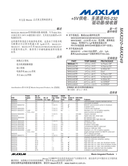
For free samples and the latest literature, visit or phone 1-800-998-8800.For small orders, phone 1-800-835-8769.General DescriptionThe MAX6361–MAX6364 supervisory circuits reduce the complexity and number of components required for power-supply monitoring and battery control functions in microprocessor (µP) systems. The circuits significantly improve system reliability and accuracy compared to that obtainable with separate ICs or discrete components.Their functions include µP reset, backup battery switchover, and power failure warning.The MAX6361–MAX6364 operate from supply voltages as low as +1.2V. The factory-preset reset threshold voltage ranges from 2.32V to 4.63V (see Ordering Information ).These devices provide a manual reset input (MAX6361),watchdog timer input (MAX6362), battery-on output (MAX6363), and an auxiliary adjustable reset input (MAX6364). In addition, each part type is offered in three reset output versions: an active-low open-drain reset, an active-low open-drain reset, and an active-high open-drain reset (see Selector Guide at end of data sheet).ApplicationsFeatures♦Low +1.2V Operating Supply Voltage (V CC or V BATT )♦Precision Monitoring of +5.0V, +3.3V, +3.0V, and +2.5V Power-Supply Voltages♦Debounced Manual Reset Input (MAX6361)♦Watchdog Timer with 1.6s Timeout Period (MAX6362)♦Battery-On Output Indicator (MAX6363)♦Auxiliary User-Adjustable RESET IN (MAX6364)♦Three Available Output StructuresPush-Pull RESET , Open-Drain RESET , Open-Drain RESET♦RESET/RESET Valid Down to 1.2V Guaranteed (V CC or V BATT )♦Power-Supply Transient Immunity ♦150ms (min) Reset Timeout Period ♦Small 6-Pin SOT23 PackageMAX6361–MAX6364SOT23, Low-Power µP Supervisory Circuitswith Battery Backup________________________________________________________________Maxim Integrated Products119-1615; Rev 3; 11/05Ordering InformationPin ConfigurationsFrom the table below, select the suffix corresponding to the desired threshold voltage and insert it into the part number to complete it. When ordering from the factory, there is a 2500-piece minimum on the SOT package (tape-and-reel only).Devices are available in both leaded and lead-free packaging.Specify lead-free by replacing "-T" with "+T" when ordering.Computers ControllersIntelligent Instruments Critical µP/µC Power MonitoringFax Machines Industrial Control POS EquipmentPortable/Battery-Powered EquipmentSelector Guide appears at end of data sheet.Typical Operating Circuit appears at end of data sheet.M A X 6361–M A X 6364SOT23, Low-Power µP Supervisory Circuits with Battery BackupABSOLUTE MAXIMUM RATINGSELECTRICAL CHARACTERISTICS(V CC = +2.4V to +5.5V, V BATT = 3V, T A = -40°C to +85°C, reset not asserted. Typical values are at T A = +25°C, unless otherwise noted.) (Note 1)Stresses beyond those listed under “Absolute Maximum Ratings” may cause permanent damage to the device. These are stress ratings only, and functional operation of the device at these or any other conditions beyond those indicated in the operational sections of the specifications is not implied. Exposure to absolute maximum rating conditions for extended periods may affect device reliability.Terminal Voltages (with respect to GND)V CC , BATT, OUT.......................................................-0.3V to +6V RESET (open drain), RESET (open drain)................-0.3V to +6V BATT ON, RESET (push-pull), RESET IN,WDI.......................................................-0.3V to (V OUT + 0.3V)MR .............................................................-0.3V to (V CC + 0.3V)Input CurrentV CC Peak ............................................................................1A V CC Continuous............................................................250mA BATT Peak....................................................................250mA BATT Continuous............................................................40mAGND................................................................................75mA Output CurrentOUT................................Short-Circuit Protection for up to 10s RESET, RESET , BATT ON ..............................................20mA Continuous Power Dissipation (T A = +70°C)6-Pin SOT23 (derate 8.70mW/°C above +70°C) .........696mW Operating Temperature Range ...........................-40°C to +85°C Junction Temperature......................................................+150°C Storage Temperature Range.............................-65°C to +150°C Lead Temperature (soldering, 10s).................................+300°CMAX6361–MAX6364SOT23, Low-Power µP Supervisory Circuitswith Battery Backup_______________________________________________________________________________________3ELECTRICAL CHARACTERISTICS (continued)(V CC = +2.4V to +5.5V, V BATT = 3V, T A = -40°C to +85°C, reset not asserted. Typical values are at T A = +25°C, unless otherwise noted.) (Note 1)Note 1:All devices are 100% production tested at T A = +25°C. Limits over temperature are guaranteed by design.Note 2:V BATT can be 0 anytime or V CC can go down to 0 if V BATT is active (except at startup).M A X 6361–M A X 6364SOT23, Low-Power µP Supervisory Circuits with Battery Backup 4_______________________________________________________________________________________Typical Operating Characteristics(T A = +25°C, unless otherwise noted.)1214161820SUPPLY CURRENT vs. TEMPERATURE(NO LOAD)TEMPERATURE (°C)S U P P L Y C U R R E N T (µA )-402040-2060800.20.60.40.81.01.2BATTERY SUPPLY CURRENT (BACKUP MODE) vs. TEMPERATURETEMPERATURE (°C)B A T T E R Y S U P P L Y C U R R E N T (µA )-402040-20060801432567BATTERY TO OUT ON-RESISTANCEvs. TEMPERATURETEMPERATURE (°C)B A T T T O O U T O N -R E S I S T A NC E (Ω)-402040-20608000.30.90.61.2V CC TO OUT ON-RESISTANCEvs. TEMPERATURETEMPERATURE (°C)V O U T T O O U T O N -R E S I S T A N C E (Ω)-402040-206080190195205200210RESET TIMEOUT PERIOD vs. TEMPERATUREM A X 6361 t o c 05TEMPERATURE (°C)R E S E T T I M E O U T P E R I O D (m s )-402040-206080301575604513512010590V CC TO RESET PROPAGATION DELAYvs. TEMPERATURETEMPERATURE (°C)P R O P A G A T I O N D E LA Y (µs )-402040-2060802.03.02.55.04.54.03.5RESET THRESHOLD vs. TEMPERATURETEMPERATURE (°C)T H R E S H O L D (V )-402040-2060801.21.41.31.61.51.91.81.72.0-40-2020406080MAX6362WATCHDOG TIMEOUT PERIODvs. TEMPERATUREM A X 6361t o c 06aTEMPERATURE (°C)W A T C H D O G T I M E O U T P E R I O D (s )1100101k10kMAXIMUM TRANSIENT DURATION vs. RESET THRESHOLD OVERDRIVERESET THRESHOLD OVERDRIVE V TH - V CC (mV)M A X I M U M T R A N S I E N T D U R A T I O N (µs )400300350250200050150100MAX6361–MAX6364SOT23, Low-Power µP Supervisory Circuitswith Battery Backup1.2341.2351.236MAX6364RESET IN THRESHOLD vs. TEMPERATUREM A X 6361 t o c 10TEMPERATURE (°C)T H R E S H O L D (V )-402040-206080Typical Operating Characteristics (continued)(T A = +25°C, unless otherwise noted.)1.01.91.61.32.82.52.2MAX6364RESET IN TO RESET PROPAGATION DELAYvs. TEMPERATURETEMPERATURE (°C)P R O P A G A T I O N D E L A Y (µs )-402040-206080Pin Description0321456789101234BATTERY SUPPLY CURRENT vs. SUPPLY VOLTAGEV CC (V)B A T T E R Y S U P P L YC U R R E N T (µA )M A X 6361–M A X 6364Detailed DescriptionThe Typical Operating Circuit shows a typical connection for the MAX6361–MAX6364 family. OUT powers the stat-ic random-access memory (SRAM). OUT is internally connected to V CC if V CC is greater than the reset thresh-old, or to the greater of V CC or V BATT when V CC is less than the reset threshold. OUT can supply up to 150mA from V CC . When V CC is higher than V BATT , the BATT ON (MAX6363) output is low. When V CC is lower than V BATT ,an internal MOSF ET connects the backup battery to OUT. The on-resistance of the MOSFET is a function of backup-battery voltage and is shown in the Battery to Out On-Resistance vs. Temperature graph in the Typical Operating Characteristics section.Backup-Battery SwitchoverIn a brownout or power failure, it may be necessary to preserve the contents of the RAM. With a backup bat-tery installed at BATT, the MAX6361–MAX6364 auto-matically switch the RAM to backup power when V CC falls. The MAX6363 has a BATT ON output that goes high when in battery-backup mode. These devices require two conditions before switching to battery-backup mode:1)V CC must be below the reset threshold.2)V CC must be below V BATT .Table 1 lists the status of the inputs and outputs in bat-tery-backup mode. The device will not power up if the only voltage source is on BATT. OUT will only power up from V CC at startup.Manual Reset Input (MAX6361 Only)Many µP-based products require manual reset capabili-ty, allowing the operator, a test technician, or external logic circuitry to initiate a reset. For the MAX6361, a logic low on MR asserts reset. Reset remains asserted while MR is low, and for a minimum of 150ms (t RP ) after it returns high. MR has an internal 20k Ωpull-up resistor to V CC . This input can be driven with TTL/CMOS logic lev-els or with open-drain/collector outputs. Connect a nor-mally open momentary switch from MR to GND to create a manual reset function; external debounce circuitry is not required. If MR is driven from long cables or the device is used in a noisy environment, connect a 0.1µF capacitor from MR to GND to provide additional noise immunity.Watchdog Input (MAX6362 Only)The watchdog monitors µP activity through the input WDI. If the µP becomes inactive, the reset output is asserted in pulses. To use the watchdog function, con-nect WDI to a bus line or µP I/O line. A change of state(high to low or low to high) within the watchdog timeout period (t WD ) with a 100ns minimum pulse width clears the watchdog timer. If WDI remains high or low for longer than the watchdog timeout period, the internal watchdog timer runs out and a reset pulse is triggered for the reset timeout period (t RP ). The internal watchdog timer clears whenever reset asserts or the WDI sees a rising or falling edge within the watchdog timeout period. If WDI remains in a high or low state for an extended period of time, a reset pulse asserts after every watchdog timeout period (t WD ) (Figure 1).Reset In (MAX6364 Only)RESET IN is compared to an internal 1.235V reference.If the voltage at RESET IN is less than 1.235V, reset is asserted. The RESET IN comparator may be used as an undervoltage detector to signal a failing power sup-ply. It can also be used as a secondary power-supply reset monitor.To program the reset threshold (V RTH ) of the secondary power supply, use the following equation (see Typical Operating Circuit ):where V REF = 1.235V. To simplify the resistor selection,choose a value for R2 and calculate R1:Since the input current at RESET IN is 25nA (max), large values (up to 1M Ω) can be used for R2 with no signifi-cant loss in accuracy. F or example, in the TypicalSOT23, Low-Power µP Supervisory Circuits with Battery Backup 6_______________________________________________________________________________________R R V V RTH REF 121 /=()−[]MAX6361–MAX6364SOT23, Low-Power µP Supervisory Circuitswith Battery Backup_______________________________________________________________________________________7Operating Circuit,the MAX6362 monitors two supply voltages. To monitor the secondary 5V logic or analog supply with a 4.60V nominal programmed reset thresh-old, choose R2 = 100k Ω, and calculate R1 = 273k Ω.Reset OutputA µP’s reset input starts the µP in a known state. The MAX6361–MAX6364 µP supervisory circuits assert a reset to prevent code-execution errors during power-up, power-down, and brownout conditions. RESET is guaranteed to be a logic low or high depending on the device chosen (see Ordering Information ). RESET or RESET asserts when V CC is below the reset threshold and for at least 150ms (t RP ) after V CC rises above the reset threshold. RESET or RESET also asserts when MR is low (MAX6361) and when RESET IN is less than 1.235V (MAX6364). The MAX6362 watchdog function will cause RESET (or RESET ) to assert in pulses follow-ing a watchdog timeout (Figure 1).Applications InformationOperation Without a BackupPower SourceThe MAX6361–MAX6364 were designed for battery-backed applications. If a backup battery is not used,connect V CC to OUT and connect BATT to GND.Replacing the Backup BatteryIf BATT is decoupled with a 0.1µF capacitor to ground,the backup power source can be removed while V CC remains valid without danger of triggering a reset pulse.The device does not enter battery-backup mode when V CC stays above the reset threshold voltage.Negative-Going V CC TransientsThese supervisors are relatively immune to short-dura-tion, negative-going V CC transients. Resetting the µPwhen V CC experiences only small glitches is usually not desirable.The Typical Operating Characteristics section shows a graph of Maximum Transient Duration vs. Reset Threshold Overdrive for which reset is not asserted.The graph was produced using negative-going V CC pulses, starting at V CC and ending below the reset threshold by the magnitude indicated (reset threshold overdrive). The graph shows the maximum pulse width that a negative-going V CC transient can typically have without triggering a reset pulse. As the amplitude of the transient increases (i.e., goes further below the reset threshold), the maximum allowable pulse width decreases. Typically, a V CC transient that goes 100mV below the reset threshold and lasts for 30µs will not trigger a reset pulse.A 0.1µF bypass capacitor mounted close to the V CC pin provides additional transient immunity.Figure 1. MAX6362 Watchdog Timeout Period and Reset Active TimeM A X 6361–M A X 6364Watchdog Software Considerations(MAX6362 Only)To help the watchdog timer monitor software execution more closely, set and reset the watchdog input at dif-ferent points in the program, rather than “pulsing” the watchdog input low-high-low. This technique avoids a “stuck” loop, in which the watchdog timer would contin-ue to be reset within the loop, keeping the watchdog from timing out. F igure 2 shows an example of a flow diagram where the I/O driving the WDI is set low at the beginning of the program, set high at the beginning of every subroutine or loop, then set low again when the program returns to the beginning. If the program should “hang” in any subroutine, the problem would quickly be corrected, since the I/O is continually set low and the watchdog timer is allowed to time out, trigger-ing a reset.SOT23, Low-Power µP Supervisory Circuits with Battery Backup 8_______________________________________________________________________________________Figure 2. Watchdog Flow DiagramMAX6361–MAX6364SOT23, Low-Power µP Supervisory Circuitswith Battery Backup_______________________________________________________________________________________9*Sample stock generally held on standard versions only. Contact factory for availability of nonstandard versions.Device Marking CodesSelector GuideM A X 6361–M A X 6364SOT23, Low-Power µP Supervisory Circuits with Battery Backup 10______________________________________________________________________________________Pin Configurations (continued)Typical Operating CircuitChip InformationTRANSISTOR COUNT: 720MAX6361–MAX6364SOT23, Low-Power µP Supervisory Circuits with Battery Backup______________________________________________________________________________________11Package InformationM A X 6361–M A X 6364SOT23, Low-Power µP Supervisory Circuits with Battery BackupMaxim cannot assume responsibility for use of any circuitry other than circuitry entirely embodied in a Maxim product. No circuit patent licenses are implied. Maxim reserves the right to change the circuitry and specifications without notice at any time.12____________________Maxim Integrated Products, 120 San Gabriel Drive, Sunnyvale, CA 94086 408-737-7600©2005 Maxim Integrated Products Printed USA is a registered trademark of Maxim Integrated Products, Inc.NOTES。