MAX472ESA-T中文资料
- 格式:pdf
- 大小:137.71 KB
- 文档页数:13
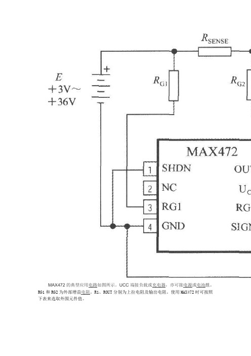
MAX472的典型应用电路如图所示。
UCC端接负载或充电器,亦可接电源或电池组。
RG1和RG2为外部增益电阻。
R1、ROUT分别为上拉电阻及输出电阻。
使用MAX472时可按照下表来选取外围元件值。
【收藏此页】【关闭】【返回】【打印】MP25P1171344:一、前言伴随着城市人口和建设规模的扩大,各种用电设备的增多,用电量越来越大,城市的供电设备经常超负荷运转,用电环境变得越来越恶劣,对电源的“考验”越来越严重。
据统计,每天,用电设备都要遭受 120 次左右各种的电源问题的侵扰,电子设备故障的 60% 来自电源 [7] 。
因此,电源问题的重要性日益凸显出来。
原先作为配角,资金投入较少的电源越来越受到厂商和研究人员的重视,电源技术遂发展成为一门崭新的技术。
而今,小小的电源设备已经融合了越来越多的新技术。
例如开关电源、硬开关、软开关、参数稳压、线性反馈稳压、磁放大器技术、数控调压、 PWM 、 SPWM 、电磁兼容等等。
实际需求直接推动电源技术不断发展和进步,为了自动检测和显示电流,并在过流、过压等危害情况发生时具有自动保护功能和更高级的智能控制,具有传感检测、传感采样、传感保护的电源技术渐成趋势,检测电流或电压的传感器便应运而生并在我国开始受到广大电源设计者的青睐,本文主要介绍 ABB 公司的电流传感器。
二、电流传感器的工作原理 [1]ABB 公司的电流传感器可以测量各种类型的电流,从直流电到几十千赫兹的交流电,其所依据的工作原理主要是霍尔效应,如图 1 所示。
当原边导线经过电流传感器时,原边电流 I P 会产生磁力线①,原边磁力线集中在磁芯②周围,内置在磁芯气隙中的霍尔电极③可产生和原边磁力线①成正比的大小仅几毫伏的电压,电子电路④可把这个微小的信号转变成副边电流 I S ⑤,并存在以下关系式其中, I S —副边电流;I P —原边电流;N P —原边线圈匝数;N S —副边线圈匝数;N P / N S —匝数比,一般取 N P =1 。

M A X471M A X472的中文资料大全(总4页)-本页仅作为预览文档封面,使用时请删除本页-MAX471/MAX472的特点、功能美国美信公司生产的精密高端电流检测放大器是一个系列化产品,有MAX471/MA X472、 MAX4172/MAX4173等。
它们均有一个电流输出端,可以用一个电阻来简单地实现以地为参考点的电流/电压的转换,并可工作在较宽电压内。
MAX471/MAX472具有如下特点:●具有完美的高端电流检测功能;●内含精密的内部检测电阻(MAX471);●在工作温度范围内,其精度为2%;●具有双向检测指示,可监控充电和放电状态;●内部检测电阻和检测能力为3A,并联使用时还可扩大检测电流范围;●使用外部检测电阻可任意扩展检测电流范围(MAX472);●最大电源电流为100μA;●关闭方式时的电流仅为5μA;●电压范围为3~36V;●采用8脚DIP/SO/STO三种封装形式。
MAX471/MAX472的引脚排列如图1所示,图2所示为其内部功能框图。
表1为MAX471/MAX472的引脚功能说明。
MAX471的电流增益比已预设为500μA/A,由于2kΩ的输出电阻(ROUT)可产生1V/A的转换,因此±3A时的满度值为3V.用不同的ROUT电阻可设置不同的满度电压。
但对于MAX471,其输出电压不应大于VRS+。
对于MAX472,则不能大于。
MAX471引脚图如图1所示,MAX472引脚图如图2所示。
MAX471/MAX472的引脚功能说明引脚名称功能MAX471MAX47211SHDN关闭端。
正常运用时连接到地。
当此端接高电平时,电源电流小于5μA2,3-RS+内部电流检测电阻电池(或电源端)。
“+”仅指示与SIGN输出有关的流动方向。
封装时已将2和3连在了一起-2空脚-3RG1增益电阻端。
通过增益设置电阻连接到电流检测电阻的电池端44GND地或电池负端55SIGN集电极开路逻辑输出端。

FEATURES AND SPECIFICATIONS SPECIIFICATIONS Battery Connector47182Vertical, SMT 47204Right Angle, SMT 47274Right Angle, SMT 47280Right Angle, SMT 48232Parallel, SMTMolex offers Battery Connectors for mobile applications.In mobile applications, battery efficiency plays an important part in the utilization time of the device. Proper battery contact, efficient electrical properties, physical size of connector are some of the major design considerations.Working together with major customers in the mobile device markets, Molex has developed a comprehensive range of battery connectors that addresses most of these applications design concerns. With working heights of 1.50mm to 5.50mm and circuit sizes of 2 to 5, Molex’s battery connectors brings forth flexibility in design solutions for the customers.4718247204472744823247280Reference InformationPackaging: Refer to order tableUL File No.:CSA File No.:Mates With:Designed In:mmElectricalVoltage: Refer to order tableCurrent: Refer to order tableContact Resistance: Refer to order tableDielectric Withstanding Voltage: Refer to ordertableInsulation Resistance: Refer to order tableMechanicalContact Insertion Force:47182, 47274, 47204 : 1.02N (0.67lb)Durability: Refer to order tablePhysicalHousing: Thoermoplastic, JL 94V-0Contact:47182, 47204, 47274, 48232 Copper (Cu)Alloy47280 Beryllium Copper (BeCu)Plating:Contact Area —Refer to order tableUnderplating—Nickel (Ni)Operating Temperature: Refer to order tableORDERING INFORMATIONBringing People & Technology Together, Worldwide SMVisit our Web site at Americas Headquarters 2222 Wellington Ct.Lisle, Illinois 60532 USA 1-800-78MOLEX amerinfo@Far East North Headquarters Yamato, Kanagawa, Japan 81-462-65-2324feninfo@Far East South Headquarters Jurong, Singapore 65-6-268-6868fesinfo@European Headquarters Munich, Germany 49-89-413092-0eurinfo@Corporate Headquarters 2222 Wellington Ct.Lisle, Illinois 60532 USA 630-969-4550MARKETS AND APPLICATIONS Order No. SNG-059©2006, MolexBattery Connector 47182Vertical, SMT 47204Right Angle, SMT 47274Right Angle, SMT 47280Right Angle, SMT 48232Parallel, SMT•Mobile phones •PDAs•Handheld GPS unitsMobile PhonesPDAsHandheld GPS。

MAX471/MAX472Precision, High-Side Current-Sense AmplifiersFigure 1. MAX471 Functional DiagramFigure 2. MAX472 Functional DiagramM A X 471/M A X 472for current summing. A single scaling resistor is required when summing OUT currents from multiple devices (Figure 3). Current can be integrated by con-necting OUT to a capacitive load.SIGN OutputThe current at OUT indicates magnitude. The SIGN out-put indicates the current’s direction. Operation of the SIGN comparator is straightforward. When Q1 (Figures 1 and 2) conducts, the output of A1 is high while A2’s output is zero. Under this condition, a high SIGN output indicates positive current flow (from RS+ to RS-). In bat-tery-operated systems, this is useful for determining whether the battery is charging or discharging. The SIGN output may not correctly indicate if the load cur-rent is such that I OUT is less than 3.5µA. The MAX471’s SIGN output accurately indicates the direction of cur-rent flow for load currents greater than 7mA.SIGN is an open-collector output (sinks current only),allowing easy interface with logic circuits powered from any voltage. Connect a 100k Ωpull-up resistor from SIGN to the logic supply. The convention chosen for the polarity of the SIGN output ensures that it draws no current when the battery is being discharged. If current direction is not needed, float the SIGN pin.Shutdown When SHDN is high, the MAX471/MAX472 are shut down and consume less than 18µA. In shutdown mode,SIGN is high impedance and OUT turns off.__________Applications Information MAX471The MAX471 obtains its power from the RS- pin. This includes MAX471 current consumption in the total sys-tem current measured by the MAX471. The small drop across R SENSE does not affect the MAX471’s perfor-mance.Resistor Selection Since OUT delivers a current, an external voltage gain-setting resistor (R OUT to ground) is required at the OUT pin in order to get a voltage. R SENSE is internal to the MAX471. RG1 and RG2 are factory trimmed for an out-put current ratio (output current to load current) of 500µA/A. Since they are manufactured of the same material and in very close proximity on the chip, they provide a high degree of temperature stability. Choose R OUT for the desired full-scale output voltage up to RS--1.5V (see the Current Output section).Precision, High-Side Current-Sense AmplifiersFigure 3. Paralleling MAX471s to Sense Higher Load Current Figure 4. MAX472 Standard Application Circuit。

For pricing, delivery, and ordering information,please contact Maxim/Dallas Direct!at 1-888-629-4642, or visit Maxim’s website at .General DescriptionThe MAX481, MAX483, MAX485, MAX487–MAX491, and MAX1487 are low-power transceivers for RS-485 and RS-422 communication. Each part contains one driver and one receiver. The MAX483, MAX487, MAX488, and MAX489feature reduced slew-rate drivers that minimize EMI and reduce reflections caused by improperly terminated cables,thus allowing error-free data transmission up to 250kbps.The driver slew rates of the MAX481, MAX485, MAX490,MAX491, and MAX1487 are not limited, allowing them to transmit up to 2.5Mbps.These transceivers draw between 120µA and 500µA of supply current when unloaded or fully loaded with disabled drivers. Additionally, the MAX481, MAX483, and MAX487have a low-current shutdown mode in which they consume only 0.1µA. All parts operate from a single 5V supply.Drivers are short-circuit current limited and are protected against excessive power dissipation by thermal shutdown circuitry that places the driver outputs into a high-imped-ance state. The receiver input has a fail-safe feature that guarantees a logic-high output if the input is open circuit.The MAX487 and MAX1487 feature quarter-unit-load receiver input impedance, allowing up to 128 MAX487/MAX1487 transceivers on the bus. Full-duplex communi-cations are obtained using the MAX488–MAX491, while the MAX481, MAX483, MAX485, MAX487, and MAX1487are designed for half-duplex applications.________________________ApplicationsLow-Power RS-485 Transceivers Low-Power RS-422 Transceivers Level TranslatorsTransceivers for EMI-Sensitive Applications Industrial-Control Local Area Networks__Next Generation Device Features♦For Fault-Tolerant ApplicationsMAX3430: ±80V Fault-Protected, Fail-Safe, 1/4Unit Load, +3.3V, RS-485 TransceiverMAX3440E–MAX3444E: ±15kV ESD-Protected,±60V Fault-Protected, 10Mbps, Fail-Safe, RS-485/J1708 Transceivers♦For Space-Constrained ApplicationsMAX3460–MAX3464: +5V, Fail-Safe, 20Mbps,Profibus RS-485/RS-422 TransceiversMAX3362: +3.3V, High-Speed, RS-485/RS-422Transceiver in a SOT23 PackageMAX3280E–MAX3284E: ±15kV ESD-Protected,52Mbps, +3V to +5.5V, SOT23, RS-485/RS-422,True Fail-Safe ReceiversMAX3293/MAX3294/MAX3295: 20Mbps, +3.3V,SOT23, RS-855/RS-422 Transmitters ♦For Multiple Transceiver ApplicationsMAX3030E–MAX3033E: ±15kV ESD-Protected,+3.3V, Quad RS-422 Transmitters ♦For Fail-Safe ApplicationsMAX3080–MAX3089: Fail-Safe, High-Speed (10Mbps), Slew-Rate-Limited RS-485/RS-422Transceivers♦For Low-Voltage ApplicationsMAX3483E/MAX3485E/MAX3486E/MAX3488E/MAX3490E/MAX3491E: +3.3V Powered, ±15kV ESD-Protected, 12Mbps, Slew-Rate-Limited,True RS-485/RS-422 TransceiversMAX481/MAX483/MAX485/MAX487–MAX491/MAX1487Low-Power, Slew-Rate-Limited RS-485/RS-422 Transceivers______________________________________________________________Selection Table19-0122; Rev 8; 10/03Ordering Information appears at end of data sheet.M A X 481/M A X 483/M A X 485/M A X 487–M A X 491/M A X 1487Low-Power, Slew-Rate-Limited RS-485/RS-422 Transceivers 2_______________________________________________________________________________________ABSOLUTE MAXIMUM RATINGSSupply Voltage (V CC ).............................................................12V Control Input Voltage (RE , DE)...................-0.5V to (V CC + 0.5V)Driver Input Voltage (DI).............................-0.5V to (V CC + 0.5V)Driver Output Voltage (A, B)...................................-8V to +12.5V Receiver Input Voltage (A, B).................................-8V to +12.5V Receiver Output Voltage (RO).....................-0.5V to (V CC +0.5V)Continuous Power Dissipation (T A = +70°C)8-Pin Plastic DIP (derate 9.09mW/°C above +70°C)....727mW 14-Pin Plastic DIP (derate 10.00mW/°C above +70°C)..800mW 8-Pin SO (derate 5.88mW/°C above +70°C).................471mW14-Pin SO (derate 8.33mW/°C above +70°C)...............667mW 8-Pin µMAX (derate 4.1mW/°C above +70°C)..............830mW 8-Pin CERDIP (derate 8.00mW/°C above +70°C).........640mW 14-Pin CERDIP (derate 9.09mW/°C above +70°C).......727mW Operating Temperature RangesMAX4_ _C_ _/MAX1487C_ A...............................0°C to +70°C MAX4__E_ _/MAX1487E_ A.............................-40°C to +85°C MAX4__MJ_/MAX1487MJA...........................-55°C to +125°C Storage Temperature Range.............................-65°C to +160°C Lead Temperature (soldering, 10sec).............................+300°CDC ELECTRICAL CHARACTERISTICS(V CC = 5V ±5%, T A = T MIN to T MAX , unless otherwise noted.) (Notes 1, 2)Stresses beyond those listed under “Absolute Maximum Ratings” may cause permanent damage to the device. These are stress ratings only, and functional operation of the device at these or any other conditions beyond those indicated in the operational sections of the specifications is not implied. Exposure to absolute maximum rating conditions for extended periods may affect device reliability.V V IN = -7VV IN = 12V V IN = -7V V IN = 12V Input Current (A, B)I IN2V TH k Ω48-7V ≤V CM ≤12V, MAX487/MAX1487R INReceiver Input Resistance -7V ≤V CM ≤12V, all devices except MAX487/MAX1487R = 27Ω(RS-485), Figure 40.4V ≤V O ≤2.4VR = 50Ω(RS-422)I O = 4mA, V ID = -200mV I O = -4mA, V ID = 200mV V CM = 0V-7V ≤V CM ≤12V DE, DI, RE DE, DI, RE MAX487/MAX1487,DE = 0V, V CC = 0V or 5.25VDE, DI, RE R = 27Ωor 50Ω, Figure 4R = 27Ωor 50Ω, Figure 4R = 27Ωor 50Ω, Figure 4DE = 0V;V CC = 0V or 5.25V,all devices except MAX487/MAX1487CONDITIONSk Ω12µA ±1I OZRThree-State (high impedance)Output Current at ReceiverV 0.4V OL Receiver Output Low Voltage 3.5V OH Receiver Output High Voltage mV 70∆V TH Receiver Input Hysteresis V -0.20.2Receiver Differential Threshold Voltage-0.2mA 0.25mA-0.81.01.55V OD2Differential Driver Output (with load)V 2V 5V OD1Differential Driver Output (no load)µA±2I IN1Input CurrentV 0.8V IL Input Low Voltage V 2.0V IH Input High Voltage V 0.2∆V OD Change in Magnitude of Driver Common-Mode Output Voltage for Complementary Output States V 0.2∆V OD Change in Magnitude of Driver Differential Output Voltage for Complementary Output States V 3V OC Driver Common-Mode Output VoltageUNITS MINTYPMAX SYMBOL PARAMETERMAX481/MAX483/MAX485/MAX487–MAX491/MAX1487Low-Power, Slew-Rate-Limited RS-485/RS-422 Transceivers_______________________________________________________________________________________3SWITCHING CHARACTERISTICS—MAX481/MAX485, MAX490/MAX491, MAX1487(V CC = 5V ±5%, T A = T MIN to T MAX , unless otherwise noted.) (Notes 1, 2)DC ELECTRICAL CHARACTERISTICS (continued)(V CC = 5V ±5%, T A = T MIN to T MAX , unless otherwise noted.) (Notes 1, 2)ns 103060t PHLDriver Rise or Fall Time Figures 6 and 8, R DIFF = 54Ω, C L1= C L2= 100pF ns MAX490M, MAX491M MAX490C/E, MAX491C/E2090150MAX481, MAX485, MAX1487MAX490M, MAX491MMAX490C/E, MAX491C/E MAX481, MAX485, MAX1487Figures 6 and 8, R DIFF = 54Ω,C L1= C L2= 100pF MAX481 (Note 5)Figures 5 and 11, C RL = 15pF, S2 closedFigures 5 and 11, C RL = 15pF, S1 closed Figures 5 and 11, C RL = 15pF, S2 closed Figures 5 and 11, C RL = 15pF, S1 closed Figures 6 and 10, R DIFF = 54Ω,C L1= C L2= 100pFFigures 6 and 8,R DIFF = 54Ω,C L1= C L2= 100pF Figures 6 and 10,R DIFF = 54Ω,C L1= C L2= 100pF CONDITIONS ns 510t SKEW ns50200600t SHDNTime to ShutdownMbps 2.5f MAX Maximum Data Rate ns 2050t HZ Receiver Disable Time from High ns 103060t PLH 2050t LZ Receiver Disable Time from Low ns 2050t ZH Driver Input to Output Receiver Enable to Output High ns 2050t ZL Receiver Enable to Output Low 2090200ns ns 134070t HZ t SKD Driver Disable Time from High |t PLH - t PHL |DifferentialReceiver Skewns 4070t LZ Driver Disable Time from Low ns 4070t ZL Driver Enable to Output Low 31540ns51525ns 31540t R , t F 2090200Driver Output Skew to Output t PLH , t PHL Receiver Input to Output4070t ZH Driver Enable to Output High UNITS MIN TYP MAX SYMBOL PARAMETERFigures 7 and 9, C L = 100pF, S2 closed Figures 7 and 9, C L = 100pF, S1 closed Figures 7 and 9, C L = 15pF, S1 closed Figures 7 and 9, C L = 15pF, S2 closedM A X 481/M A X 483/M A X 485/M A X 487–M A X 491/M A X 1487Low-Power, Slew-Rate-Limited RS-485/RS-422 Transceivers 4_______________________________________________________________________________________SWITCHING CHARACTERISTICS—MAX483, MAX487/MAX488/MAX489(V CC = 5V ±5%, T A = T MIN to T MAX , unless otherwise noted.) (Notes 1, 2)SWITCHING CHARACTERISTICS—MAX481/MAX485, MAX490/MAX491, MAX1487 (continued)(V CC = 5V ±5%, T A = T MIN to T MAX , unless otherwise noted.) (Notes 1, 2)3001000Figures 7 and 9, C L = 100pF, S2 closed Figures 7 and 9, C L = 100pF, S1 closed Figures 5 and 11, C L = 15pF, S2 closed,A - B = 2VCONDITIONSns 40100t ZH(SHDN)Driver Enable from Shutdown toOutput High (MAX481)nsFigures 5 and 11, C L = 15pF, S1 closed,B - A = 2Vt ZL(SHDN)Receiver Enable from Shutdownto Output Low (MAX481)ns 40100t ZL(SHDN)Driver Enable from Shutdown toOutput Low (MAX481)ns 3001000t ZH(SHDN)Receiver Enable from Shutdownto Output High (MAX481)UNITS MINTYP MAX SYMBOLPARAMETERt PLH t SKEW Figures 6 and 8, R DIFF = 54Ω,C L1= C L2= 100pFt PHL Figures 6 and 8, R DIFF = 54Ω,C L1= C L2= 100pFDriver Input to Output Driver Output Skew to Output ns 100800ns ns 2000MAX483/MAX487, Figures 7 and 9,C L = 100pF, S2 closedt ZH(SHDN)Driver Enable from Shutdown to Output High2502000ns2500MAX483/MAX487, Figures 5 and 11,C L = 15pF, S1 closedt ZL(SHDN)Receiver Enable from Shutdown to Output Lowns 2500MAX483/MAX487, Figures 5 and 11,C L = 15pF, S2 closedt ZH(SHDN)Receiver Enable from Shutdown to Output Highns 2000MAX483/MAX487, Figures 7 and 9,C L = 100pF, S1 closedt ZL(SHDN)Driver Enable from Shutdown to Output Lowns 50200600MAX483/MAX487 (Note 5) t SHDN Time to Shutdownt PHL t PLH , t PHL < 50% of data period Figures 5 and 11, C RL = 15pF, S2 closed Figures 5 and 11, C RL = 15pF, S1 closed Figures 5 and 11, C RL = 15pF, S2 closed Figures 5 and 11, C RL = 15pF, S1 closed Figures 7 and 9, C L = 15pF, S2 closed Figures 6 and 10, R DIFF = 54Ω,C L1= C L2= 100pFFigures 7 and 9, C L = 15pF, S1 closed Figures 7 and 9, C L = 100pF, S1 closed Figures 7 and 9, C L = 100pF, S2 closed CONDITIONSkbps 250f MAX 2508002000Maximum Data Rate ns 2050t HZ Receiver Disable Time from High ns 25080020002050t LZ Receiver Disable Time from Low ns 2050t ZH Receiver Enable to Output High ns 2050t ZL Receiver Enable to Output Low ns ns 1003003000t HZ t SKD Driver Disable Time from High I t PLH - t PHL I DifferentialReceiver SkewFigures 6 and 10, R DIFF = 54Ω,C L1= C L2= 100pFns 3003000t LZ Driver Disable Time from Low ns 2502000t ZL Driver Enable to Output Low ns Figures 6 and 8, R DIFF = 54Ω,C L1= C L2= 100pFns 2502000t R , t F 2502000Driver Rise or Fall Time ns t PLH Receiver Input to Output2502000t ZH Driver Enable to Output High UNITS MIN TYP MAX SYMBOL PARAMETERMAX481/MAX483/MAX485/MAX487–MAX491/MAX1487Low-Power, Slew-Rate-Limited RS-485/RS-422 Transceivers_______________________________________________________________________________________530002.5OUTPUT CURRENT vs.RECEIVER OUTPUT LOW VOLTAGE525M A X 481-01OUTPUT LOW VOLTAGE (V)O U T P U T C U R R E N T (m A )1.515100.51.02.0203540450.90.1-50-252575RECEIVER OUTPUT LOW VOLTAGE vs.TEMPERATURE0.30.7TEMPERATURE (°C)O U T P U TL O W V O L T A G E (V )500.50.80.20.60.40100125-20-41.5 2.0 3.0 5.0OUTPUT CURRENT vs.RECEIVER OUTPUT HIGH VOLTAGE-8-16M A X 481-02OUTPUT HIGH VOLTAGE (V)O U T P U T C U R R E N T (m A )2.5 4.0-12-18-6-14-10-203.54.5 4.83.2-50-252575RECEIVER OUTPUT HIGH VOLTAGE vs.TEMPERATURE3.64.4TEMPERATURE (°C)O U T P UT H I G H V O L T A G E (V )0504.04.63.44.23.83.01001259000 1.0 3.0 4.5DRIVER OUTPUT CURRENT vs.DIFFERENTIAL OUTPUT VOLTAGE1070M A X 481-05DIFFERENTIAL OUTPUT VOLTAGE (V)O U T P U T C U R R E N T (m A )2.0 4.05030806040200.5 1.5 2.53.5 2.31.5-50-2525125DRIVER DIFFERENTIAL OUTPUT VOLTAGEvs. TEMPERATURE1.72.1TEMPERATURE (°C)D I F FE R E N T I A L O U T P U T V O L T A G E (V )751.92.21.62.01.8100502.4__________________________________________Typical Operating Characteristics(V CC = 5V, T A = +25°C, unless otherwise noted.)NOTES FOR ELECTRICAL/SWITCHING CHARACTERISTICSNote 1:All currents into device pins are positive; all currents out of device pins are negative. All voltages are referenced to deviceground unless otherwise specified.Note 2:All typical specifications are given for V CC = 5V and T A = +25°C.Note 3:Supply current specification is valid for loaded transmitters when DE = 0V.Note 4:Applies to peak current. See Typical Operating Characteristics.Note 5:The MAX481/MAX483/MAX487 are put into shutdown by bringing RE high and DE low. If the inputs are in this state for lessthan 50ns, the parts are guaranteed not to enter shutdown. If the inputs are in this state for at least 600ns, the parts are guaranteed to have entered shutdown. See Low-Power Shutdown Mode section.M A X 481/M A X 483/M A X 485/M A X 487–M A X 491/M A X 1487Low-Power, Slew-Rate-Limited RS-485/RS-422 Transceivers 6___________________________________________________________________________________________________________________Typical Operating Characteristics (continued)(V CC = 5V, T A = +25°C, unless otherwise noted.)120008OUTPUT CURRENT vs.DRIVER OUTPUT LOW VOLTAGE20100M A X 481-07OUTPUT LOW VOLTAGE (V)O U T P U T C U R R E N T (m A )6604024801012140-1200-7-5-15OUTPUT CURRENT vs.DRIVER OUTPUT HIGH VOLTAGE-20-80M A X 481-08OUTPUT HIGH VOLTAGE (V)O U T P U T C U R R E N T (m A )-31-603-6-4-2024-100-40100-40-60-2040100120MAX1487SUPPLY CURRENT vs. TEMPERATURE300TEMPERATURE (°C)S U P P L Y C U R R E N T (µA )20608050020060040000140100-50-2550100MAX481/MAX485/MAX490/MAX491SUPPLY CURRENT vs. TEMPERATURE300TEMPERATURE (°C)S U P P L Y C U R R E N T (µA )257550020060040000125100-50-2550100MAX483/MAX487–MAX489SUPPLY CURRENT vs. TEMPERATURE300TEMPERATURE (°C)S U P P L Y C U R R E N T (µA )257550020060040000125MAX481/MAX483/MAX485/MAX487–MAX491/MAX1487Low-Power, Slew-Rate-Limited RS-485/RS-422 Transceivers_______________________________________________________________________________________7______________________________________________________________Pin DescriptionFigure 1. MAX481/MAX483/MAX485/MAX487/MAX1487 Pin Configuration and Typical Operating CircuitM A X 481/M A X 483/M A X 485/M A X 487–M A X 491/M A X 1487__________Applications InformationThe MAX481/MAX483/MAX485/MAX487–MAX491 and MAX1487 are low-power transceivers for RS-485 and RS-422 communications. The MAX481, MAX485, MAX490,MAX491, and MAX1487 can transmit and receive at data rates up to 2.5Mbps, while the MAX483, MAX487,MAX488, and MAX489 are specified for data rates up to 250kbps. The MAX488–MAX491 are full-duplex trans-ceivers while the MAX481, MAX483, MAX485, MAX487,and MAX1487 are half-duplex. In addition, Driver Enable (DE) and Receiver Enable (RE) pins are included on the MAX481, MAX483, MAX485, MAX487, MAX489,MAX491, and MAX1487. When disabled, the driver and receiver outputs are high impedance.MAX487/MAX1487:128 Transceivers on the BusThe 48k Ω, 1/4-unit-load receiver input impedance of the MAX487 and MAX1487 allows up to 128 transceivers on a bus, compared to the 1-unit load (12k Ωinput impedance) of standard RS-485 drivers (32 trans-ceivers maximum). Any combination of MAX487/MAX1487 and other RS-485 transceivers with a total of 32 unit loads or less can be put on the bus. The MAX481/MAX483/MAX485 and MAX488–MAX491 have standard 12k ΩReceiver Input impedance.Low-Power, Slew-Rate-Limited RS-485/RS-422 Transceivers 8_______________________________________________________________________________________Figure 2. MAX488/MAX490 Pin Configuration and Typical Operating CircuitFigure 3. MAX489/MAX491 Pin Configuration and Typical Operating CircuitMAX483/MAX487/MAX488/MAX489:Reduced EMI and ReflectionsThe MAX483 and MAX487–MAX489 are slew-rate limit-ed, minimizing EMI and reducing reflections caused by improperly terminated cables. Figure 12 shows the dri-ver output waveform and its Fourier analysis of a 150kHz signal transmitted by a MAX481, MAX485,MAX490, MAX491, or MAX1487. High-frequency har-monics with large amplitudes are evident. Figure 13shows the same information displayed for a MAX483,MAX487, MAX488, or MAX489 transmitting under the same conditions. Figure 13’s high-frequency harmonics have much lower amplitudes, and the potential for EMI is significantly reduced.MAX481/MAX483/MAX485/MAX487–MAX491/MAX1487Low-Power, Slew-Rate-Limited RS-485/RS-422 Transceivers_______________________________________________________________________________________9_________________________________________________________________Test CircuitsFigure 4. Driver DC Test Load Figure 5. Receiver Timing Test LoadFigure 6. Driver/Receiver Timing Test Circuit Figure 7. Driver Timing Test LoadM A X 481/M A X 483/M A X 485/M A X 487–M A X 491/M A X 1487Low-Power, Slew-Rate-Limited RS-485/RS-422 Transceivers 10_______________________________________________________Switching Waveforms_________________Function Tables (MAX481/MAX483/MAX485/MAX487/MAX1487)Figure 8. Driver Propagation DelaysFigure 9. Driver Enable and Disable Times (except MAX488 and MAX490)Figure 10. Receiver Propagation DelaysFigure 11. Receiver Enable and Disable Times (except MAX488and MAX490)Table 1. TransmittingTable 2. ReceivingLow-Power Shutdown Mode (MAX481/MAX483/MAX487)A low-power shutdown mode is initiated by bringing both RE high and DE low. The devices will not shut down unless both the driver and receiver are disabled.In shutdown, the devices typically draw only 0.1µA of supply current.RE and DE may be driven simultaneously; the parts are guaranteed not to enter shutdown if RE is high and DE is low for less than 50ns. If the inputs are in this state for at least 600ns, the parts are guaranteed to enter shutdown.For the MAX481, MAX483, and MAX487, the t ZH and t ZL enable times assume the part was not in the low-power shutdown state (the MAX485/MAX488–MAX491and MAX1487 can not be shut down). The t ZH(SHDN)and t ZL(SHDN)enable times assume the parts were shut down (see Electrical Characteristics ).It takes the drivers and receivers longer to become enabled from the low-power shutdown state (t ZH(SHDN ), t ZL(SHDN)) than from the operating mode (t ZH , t ZL ). (The parts are in operating mode if the –R —E –,DE inputs equal a logical 0,1 or 1,1 or 0, 0.)Driver Output ProtectionExcessive output current and power dissipation caused by faults or by bus contention are prevented by two mechanisms. A foldback current limit on the output stage provides immediate protection against short cir-cuits over the whole common-mode voltage range (see Typical Operating Characteristics ). In addition, a ther-mal shutdown circuit forces the driver outputs into a high-impedance state if the die temperature rises excessively.Propagation DelayMany digital encoding schemes depend on the differ-ence between the driver and receiver propagation delay times. Typical propagation delays are shown in Figures 15–18 using Figure 14’s test circuit.The difference in receiver delay times, | t PLH - t PHL |, is typically under 13ns for the MAX481, MAX485,MAX490, MAX491, and MAX1487 and is typically less than 100ns for the MAX483 and MAX487–MAX489.The driver skew times are typically 5ns (10ns max) for the MAX481, MAX485, MAX490, MAX491, and MAX1487, and are typically 100ns (800ns max) for the MAX483 and MAX487–MAX489.MAX481/MAX483/MAX485/MAX487–MAX491/MAX1487Low-Power, Slew-Rate-Limited RS-485/RS-422 Transceivers______________________________________________________________________________________1110dB/div0Hz5MHz500kHz/div10dB/div0Hz5MHz500kHz/divFigure 12. Driver Output Waveform and FFT Plot of MAX481/MAX485/MAX490/MAX491/MAX1487 Transmitting a 150kHz SignalFigure 13. Driver Output Waveform and FFT Plot of MAX483/MAX487–MAX489 Transmitting a 150kHz SignalM A X 481/M A X 483/M A X 485/M A X 487–M A X 491/M A X 1487Low-Power, Slew-Rate-Limited RS-485/RS-422 Transceivers 12______________________________________________________________________________________V CC = 5V T A = +25°CV CC = 5V T A = +25°CV CC = 5V T A = +25°CV CC = 5V T A = +25°CFigure 14. Receiver Propagation Delay Test CircuitFigure 15. MAX481/MAX485/MAX490/MAX491/MAX1487Receiver t PHLFigure 16. MAX481/MAX485/MAX490/MAX491/MAX1487Receiver t PLHPHL Figure 18. MAX483, MAX487–MAX489 Receiver t PLHLine Length vs. Data RateThe RS-485/RS-422 standard covers line lengths up to 4000 feet. For line lengths greater than 4000 feet, see Figure 23.Figures 19 and 20 show the system differential voltage for the parts driving 4000 feet of 26AWG twisted-pair wire at 110kHz into 120Ωloads.Typical ApplicationsThe MAX481, MAX483, MAX485, MAX487–MAX491, and MAX1487 transceivers are designed for bidirectional data communications on multipoint bus transmission lines.Figures 21 and 22 show typical network applications circuits. These parts can also be used as line repeaters, with cable lengths longer than 4000 feet, as shown in Figure 23.To minimize reflections, the line should be terminated at both ends in its characteristic impedance, and stub lengths off the main line should be kept as short as possi-ble. The slew-rate-limited MAX483 and MAX487–MAX489are more tolerant of imperfect termination.MAX481/MAX483/MAX485/MAX487–MAX491/MAX1487Low-Power, Slew-Rate-Limited RS-485/RS-422 Transceivers______________________________________________________________________________________13DIV Y -V ZRO5V 0V1V0V -1V5V 0V2µs/divFigure 19. MAX481/MAX485/MAX490/MAX491/MAX1487 System Differential Voltage at 110kHz Driving 4000ft of Cable Figure 20. MAX483, MAX487–MAX489 System Differential Voltage at 110kHz Driving 4000ft of CableFigure 21. MAX481/MAX483/MAX485/MAX487/MAX1487 Typical Half-Duplex RS-485 NetworkM A X 481/M A X 483/M A X 485/M A X 487–M A X 491/M A X 1487Low-Power, Slew-Rate-Limited RS-485/RS-422 Transceivers 14______________________________________________________________________________________Figure 22. MAX488–MAX491 Full-Duplex RS-485 NetworkFigure 23. Line Repeater for MAX488–MAX491Isolated RS-485For isolated RS-485 applications, see the MAX253 and MAX1480 data sheets.MAX481/MAX483/MAX485/MAX487–MAX491/MAX1487Low-Power, Slew-Rate-Limited RS-485/RS-422 Transceivers______________________________________________________________________________________15_______________Ordering Information_________________Chip TopographiesMAX481/MAX483/MAX485/MAX487/MAX1487N.C. RO 0.054"(1.372mm)0.080"(2.032mm)DE DIGND B N.C.V CCARE * Contact factory for dice specifications.__Ordering Information (continued)M A X 481/M A X 483/M A X 485/M A X 487–M A X 491/M A X 1487Low-Power, Slew-Rate-Limited RS-485/RS-422 Transceivers 16______________________________________________________________________________________TRANSISTOR COUNT: 248SUBSTRATE CONNECTED TO GNDMAX488/MAX490B RO 0.054"(1.372mm)0.080"(2.032mm)N.C. DIGND Z A V CCYN.C._____________________________________________Chip Topographies (continued)MAX489/MAX491B RO 0.054"(1.372mm)0.080"(2.032mm)DE DIGND Z A V CCYREMAX481/MAX483/MAX485/MAX487–MAX491/MAX1487Low-Power, Slew-Rate-Limited RS-485/RS-422 Transceivers______________________________________________________________________________________17Package Information(The package drawing(s) in this data sheet may not reflect the most current specifications. For the latest package outline information go to /packages .)S O I C N .E P SM A X 481/M A X 483/M A X 485/M A X 487–M A X 491/M A X 1487Low-Power, Slew-Rate-Limited RS-485/RS-422 Transceivers 18______________________________________________________________________________________Package Information (continued)(The package drawing(s) in this data sheet may not reflect the most current specifications. For the latest package outline information go to /packages .)MAX481/MAX483/MAX485/MAX487–MAX491Low-Power, Slew-Rate-Limited RS-485/RS-422 TransceiversMaxim cannot assume responsibility for use of any circuitry other than circuitry entirely embodied in a Maxim product. No circuit patent licenses are implied. Maxim reserves the right to change the circuitry and specifications without notice at any time.Maxim Integrated Products, 120 San Gabriel Drive, Sunnyvale, CA 94086 408-737-7600 ____________________19©2003 Maxim Integrated ProductsPrinted USAis a registered trademark of Maxim Integrated Products.M A X 481/M A X 483/M A X 485/M A X 487–M A X 491/M A X 1487P D I P N .E PSPackage Information (continued)(The package drawing(s) in this data sheet may not reflect the most current specifications. For the latest package outline information go to /packages .)。


_______________General DescriptionThe MAX471/MAX472 are complete, bidirectional, high-side current-sense amplifiers for portable PCs, tele-phones, and other systems where battery/DC power-line monitoring is critical. High-side power-line monitoring is especially useful in battery-powered sys-tems, since it does not interfere with the ground paths of the battery chargers or monitors often found in “smart” batteries.The MAX471 has an internal 35m Ωcurrent-sense resis-tor and measures battery currents up to ±3A. For appli-cations requiring higher current or increased flexibility,the MAX472 functions with external sense and gain-set-ting resistors. Both devices have a current output that can be converted to a ground-referred voltage with a single resistor, allowing a wide range of battery volt-ages and currents.An open-collector SIGN output indicates current-flow direction, so the user can monitor whether a battery is being charged or discharged. Both devices operate from 3V to 36V, draw less than 100µA over tempera-ture, and include a 18µA max shutdown mode.________________________ApplicationsPortable PCs:Notebooks/Subnotebooks/Palmtops Smart Battery Packs Cellular Phones Portable PhonesPortable Test/Measurement Systems Battery-Operated Systems Energy Management Systems____________________________Featureso Complete High-Side Current Sensing o Precision Internal Sense Resistor (MAX471)o 2% Accuracy Over Temperature o Monitors Both Charge and Dischargeo 3A Sense Capability with Internal Sense Resistor (MAX471)o Higher Current-Sense Capability with External Sense Resistor (MAX472)o 100µA Max Supply Current o 18µA Max Shutdown Mode o 3V to 36V Supply Operation o 8-Pin DIP/SO Packages______________Ordering InformationMAX471/MAX472Precision, High-Side Current-Sense Amplifiers________________________________________________________________Maxim Integrated Products1_________________Pin Configurations__________Typical Operating Circuit19-0335; Rev 2; 12/96For free samples & the latest literature: , or phone 1-800-998-8800M A X 471/M A X 472Precision, High-SideCurrent-Sense AmplifiersABSOLUTE MAXIMUM RATINGSELECTRICAL CHARACTERISTICS—MAX471(RS+ = +3V to +36V, T A = T MIN to T MAX , unless otherwise noted. Typical values are at T A = +25°C.)Stresses beyond those listed under “Absolute Maximum Ratings” may cause permanent damage to the device. These are stress ratings only, and functional operation of the device at these or any other conditions beyond those indicated in the operational sections of the specifications is not implied. Exposure to absolute maximum rating conditions for extended periods may affect device reliability.Supply Voltage, RS+, RS-, V CC to GND....................-0.3V, +40V RMS Current, RS+ to RS- (MAX471 only)..........................±3.3A Peak Current, (RS+ to RS-)......................................see Figure 5Differential Input Voltage, RG1 to RG2 (MAX472 only) .....±0.3V Voltage at Any Pin Except SIGNMAX471 only...........................................-0.3V to (RS+ - 0.3V)MAX472 only..........................................-0.3V to (V CC + 0.3V)Voltage at SIGN......................................................-0.3V to +40V Current into SHDN, GND, OUT, RG1, RG2, V CC ................±50mA Current into SIGN.................................................+10mA, -50mAContinuous Power Dissipation (T A = +70°C)MAX471 (Note 1):Plastic DIP (derate 17.5mW/°C above +70°C)..................1.4W SO (derate 9.9mW/°C above +70°C).............................791mW MAX472 :Plastic DIP (derate 9.09mW/°C above +70°C)..............727mW SO (derate 5.88mW/°C above +70°C)...........................471mW Operating Temperature RangesMAX47_C_A........................................................0°C to +70°C MAX47_E_A.....................................................-40°C to +85°C Junction Temperature Range............................-60°C to +150°C Storage Temperature Range.............................-60°C to +160°C Lead Temperature (soldering, 10sec).............................+300°CNote 1:Due to special packaging considerations, MAX471 (DIP, SO) has a higher power dissipation rating than the MAX472. RS+and RS- must be soldered to large copper traces to achieve this dissipation rating.MAX471/MAX472Precision, High-Side Current-Sense Amplifiers_______________________________________________________________________________________3ELECTRICAL CHARACTERISTICS—MAX472(V CC = +3V to +36V, RG1 = RG2 = 200Ω, T A = T MIN to T MAX , unless otherwise noted. Typical values are at T A = +25°C.)Note 2:V OS is defined as the input voltage (V SENSE ) required to give minimum I OUT .Note 3:V SENSE is the voltage across the sense resistor.M A X 471/M A X 472Precision, High-SideCurrent-Sense Amplifiers 4_________________________________________________________________________________________________________________________________Typical Operating Characteristics(Typical Operating Circuit (MAX471) or circuit of Figure 4, RG1 = RG2 = 200Ω, R OUT = 2k Ω(MAX472), T A = +25°C, unless otherwise noted.)6535SUPPLY CURRENT vs. SUPPLY VOLTAGE40V RS+ (V)S U P P L Y C U R R E N T (µA )212415189123627303336455055602.500.52.0I S H D N (µA )1.51.0SHUTDOWN CURRENT vs. SUPPLY VOLTAGEV RS+(V)2124151891236273033364-2SIGN THRESHOLD vs. SUPPLY VOLTAGE-1S I G N T H R E S H O L D (m A )2124151891236273033360123V RS+ (V)0.6O F F S E T C U R R E N T (µA )MAX471NO-LOAD OFFSET CURRENT vs.SUPPLY VOLTAGEV RS+ (V)2124151891236273033360.81.01.21.41.61.82.02.22.428-4080TEMPERATURE (°C)R E S I S T A N C E (m Ω)2030-206040M A X 1471-07MAX471RS+ TO RS- RESISTANCE vs.TEMPERATURE3234363840-120.010.10MAX471ERROR vs. LOAD CURRENTI LOAD (A)E R R O R (%)110-15-6-9-303691215400.01101000MAX471POWER-SUPPLY REJECTION RATIOvs. FREQUENCYPOWER-SUPPLY FREQUENCY (kHz)P S R R (%)1100353025201510500.103.00MAX472NO-LOAD OUTPUT ERROR vs.SUPPLY VOLTAGE0.5V CC (V)IO U T (µA )2124151891236273033361.01.52.02.50.70E R R O R (%)MAX472ERROR vs. SUPPLY VOLTAGEV CC (V)2124151891236273033360.800.901.001.10MAX471/MAX472Precision, High-Side Current-Sense Amplifiers_______________________________________________________________________________________525-250.1101000MAX472ERROR vs. SENSE VOLTAGEV SENSE (mV)E R R O R (%)1550-5-1511001mA10mA100mA1A0.100.20.30.40.5MAX471 NOISE vs. LOAD C URRENTI SENSEI O U T N O I S E (µA R M S )M A X 471-15____________________________Typical Operating Characteristics (continued)(Typical Operating Circuit (MAX471) or circuit of Figure 4, RG1 = RG2 = 200Ω, R OUT = 2k Ω(MAX472), T A = +25°C, unless otherwise noted.)100µs/divV CC = 10V, R OUT = 2k Ω 1%, SIGN PULL-UP = 50k Ω 1%LOAD CURRENT 50mA/div V OUT 50mV/divMAX4710mA to 100mA TRANSIENT RESPONSE0A10µs/divI LOAD = 1A, R OUT = 2k Ω 1%V OUT500mV/div MAX471 START-UP DELAY V SHDN 5V/div10µs/divR OUT = 2k Ω 1%I LOAD 1A/divMAX4710A TO 3A TRANSIENT RESPONSEV OUT 10mV/div100µs/divV CC = 10V, R OUT = 2k Ω 1%, SIGN PULL-UP = 50k Ω 1%LOAD CURRENT 100mA/div50mA/div V OUT 50mV/divMAX471-100mA to +100mA TRANSIENT RESPONSESIGN 50mV/div0AM A X 471/M A X 472_______________Detailed DescriptionThe MAX471 and MAX472 current-sense amplifier’s unique topology allows a simple design to accurately monitor current flow. The MAX471/MAX472 contain two amplifiers operating as shown in Figures 1 and 2. The battery/load current flows from RS+ to RS- (or vice versa) through R SENSE . Current flows through either RG1 and Q1 or RG2 and Q2, depending on the sense-resistor current direction. Internal circuitry, not shown in Figures 1 and 2, prevents Q1 and Q2 from turning on at the same time. The MAX472 is identical to the MAX471, except that R SENSE and gain-setting resistors RG1 and RG2 are external (Figure 2).To analyze the circuit of Figure 1, assume that current flows from RS+ to RS- and that OUT is connected to GND through a resistor. In this case, amplifier A1 is active and output current I OUT flows from the emitter of Q1. Since no current flows through RG2 (Q2 is off), the negative input of A1 is equal to V SOURCE - (I LOAD x R SENSE ). The open-loop gain of A1 forces its positive input to essentially the same level as the negative input.Therefore, the drop across RG1 equals I LOAD x R SENSE . Then, since I OUT flows through Q1 and RG (ignoring the extremely low base currents), I OUT x RG1= I LOAD x R SENSE , or:I OUT = (I LOAD x R SENSE )/ RG1Current OutputThe output voltage equation for the MAX471/MAX472 is given below. In the MAX471, the current-gain ratio has been preset to 500µA/A so that an output resistor (R OUT ) of 2k Ωyields 1V/A for a full-scale value of +3V at ±3A. Other full-scale voltages can be set with differ-ent R OUT values, but the output voltage can be no greater than V RS+- 1.5V for the MAX471 or V RG_- 1.5V for the MAX472.V OUT = (R SENSE x R OUT x I LOAD ) / RGwhere V OUT = the desired full-scale output voltage,I LOAD = the full-scale current being sensed, R SENSE =the current-sense resistor, R OUT = the voltage-setting resistor, and RG = the gain-setting resistor (RG = RG1= RG2).The above equation can be modified to determine the R OUT required for a particular full-scale range:R OUT = (V OUT x RG) / (I LOAD x R SENSE )For the MAX471, this reduces to:R OUT = V OUT / (I LOAD x 500µA/A)OUT is a high-impedance current-source output that can be connected to other MAX471/MAX472 OUT pinsPrecision, High-SideCurrent-Sense Amplifiers 6_____________________________________________________________________________________________________________________________________________________Pin DescriptionMAX471/MAX472Precision, High-Side Current-Sense Amplifiers_______________________________________________________________________________________7Figure 1. MAX471 Functional DiagramFigure 2. MAX472 Functional DiagramM A X 471/M A X 472for current summing. A single scaling resistor is required when summing OUT currents from multiple devices (Figure 3). Current can be integrated by con-necting OUT to a capacitive load.SIGN OutputThe current at OUT indicates magnitude. The SIGN out-put indicates the current’s direction. Operation of the SIGN comparator is straightforward. When Q1 (Figures 1 and 2) conducts, the output of A1 is high while A2’s output is zero. Under this condition, a high SIGN output indicates positive current flow (from RS+ to RS-). In bat-tery-operated systems, this is useful for determining whether the battery is charging or discharging. The SIGN output may not correctly indicate if the load cur-rent is such that I OUT is less than 3.5µA. The MAX471’s SIGN output accurately indicates the direction of cur-rent flow for load currents greater than 7mA.SIGN is an open-collector output (sinks current only),allowing easy interface with logic circuits powered from any voltage. Connect a 100k Ωpull-up resistor from SIGN to the logic supply. The convention chosen for the polarity of the SIGN output ensures that it draws no current when the battery is being discharged. If current direction is not needed, float the SIGN pin.ShutdownWhen SHDN is high, the MAX471/MAX472 are shut down and consume less than 18µA. In shutdown mode,SIGN is high impedance and OUT turns off.__________Applications InformationMAX471The MAX471 obtains its power from the RS- pin. This includes MAX471 current consumption in the total sys-tem current measured by the MAX471. The small drop across R SENSE does not affect the MAX471’s perfor-mance.Resistor SelectionSince OUT delivers a current, an external voltage gain-setting resistor (R OUT to ground) is required at the OUT pin in order to get a voltage. R SENSE is internal to the MAX471. RG1 and RG2 are factory trimmed for an out-put current ratio (output current to load current) of 500µA/A. Since they are manufactured of the same material and in very close proximity on the chip, they provide a high degree of temperature stability. Choose R OUT for the desired full-scale output voltage up to RS-- 1.5V (see the Current Output section).Precision, High-SideCurrent-Sense Amplifiers 8_______________________________________________________________________________________Figure 3. Paralleling MAX471s to Sense Higher Load Current Figure 4. MAX472 Standard Application CircuitPeak Sense CurrentThe MAX471’s maximum sense current is 3A RMS . For power-up, fault conditions, or other infrequent events,MAX472R SENSE , RG1, and RG2 are externally connected on the MAX472. V CC can be connected to either the load/charge or power-source/battery side of the sense resistor. Connect V CC to the load/charge side of R SENSE if you want to include the MAX472 current drain in the measured current.Suggested Component Valuesfor Various ApplicationsThe general circuit of Figure 4 is useful in a wide variety of applications. It can be used for high-current applica-tions (greater than 3A), and also for those where the full-scale load current is less than the 3A of the MAX471.Table 1 shows suggested component values and indi-cates the resulting scale factors for various applications required to sense currents from 100mA to 10A.Higher or lower sense-current circuits can also be built.Select components and calculate circuit errors using the guidelines and formulas in the following section.R SENSEChoose R SENSE based on the following criteria:a)Voltage Loss: A high R SENSE value will cause the power-source voltage to degrade through IR loss.For least voltage loss, use the lowest R SENSE value.b)Accuracy: A high R SENSE value allows lower currents to be measured more accurately. This is because offsets become less significant when the sense voltage is larger.c)Efficiency and Power Dissipation:At high current levels, the I 2R losses in R SENSE may be significant.Take this into consideration when choosing the resistor value and power dissipation (wattage) rat-ing. Also, if the sense resistor is allowed to heat up excessively, its value may drift.d)Inductance:If there is a large high-frequency com-ponent to I SENSE , you will want to keep inductance low. Wire-wound resistors have the highest induc-tance, while metal film is somewhat better. Low-inductance metal-film resistors are available. Instead of being spiral wrapped around a core, as in metal-film or wire-wound resistors, these are a straight band of metal. They are made in values under 1Ω.e)Cost:If the cost of R SENSE becomes an issue, you may want to use an alternative solution, as shown in Figure 6. This solution uses the PC board traces to create a sense resistor. Because of the inaccuracies of the copper “resistor,” you will need to adjust the full-scale current value with a potentiometer. Also,the resistance temperature coefficient of copper is fairly high (approximately 0.4%/°C), so systems that experience a wide temperature variance should take this into account.MAX471/MAX472Precision, High-Side Current-Sense AmplifiersTable 1. Suggested Component Values for the MAX472M A X 471/M A X 472In Figure 6, assume the load current to be measured is 10A and that you have determined a 0.3 inch wide, 2ounce copper to be appropriate. The resistivity of 0.1inch wide, 2 ounce copper is 30m Ω/ft (see Note 4). For 10A you may want R SENSE = 5m Ωfor a 50mV drop at full scale. This resistor will require about 2 inches of 0.1inch wide copper trace.RG1 and RG2Once R SENSE is chosen, RG1 and RG2 can be chosen to define the current-gain ratio (R SENSE /RG). Choose RG = RG1 = RG2 based on the following criteria:a)1ΩInput Resistance.The minimum RG value is lim-ited by the 1Ωinput resistance, and also by the out-put current limitation (see below). As RG is reduced,the input resistance becomes a larger portion of the total gain-setting resistance. With RG = 50Ω, the input resistance produces a 2% difference between the expected and actual current-gain ratio. This is a gain error that does not affect linearity and can be removed by adjusting RG or R OUT .b)Efficiency.As RG is reduced, I OUT gets larger for a given load current. Power dissipated in R OUT is not going to the load, and therefore reduces overall effi-ciency. This is significant only when the sense cur-rent is small.c)Maximum Output Current Limitation.I OUT is limit-ed to 1.5mA, requiring RG ≥V SENSE / 1.5mA. For V SENSE = 60mV, RG must be ≥40Ω.d)Headroom.The MAX472 requires a minimum of 1.5V between the lower of the voltage at RG1 or RG2 (V RG_) and V OUT . As RG becomes larger, the voltage drop across RG also becomes larger for a given I OUT . This voltage drop further limits the maxi-mum full-scale V OUT . Assuming the drop across R SENSE is small and V CC is connected to either side of R SENSE , V OUT (max) = V CC - (1.5V + I OUT (max) x RG).e)Output Offset Error at Low Load rge RG values reduce I OUT for a given load current. As I OUT gets smaller, the 2.5µA max output offset-error current becomes a larger part of the overall output current. Keeping the gain high by choosing a low value for RG minimizes this offset error.f)Input Bias Current and Input Bias Current Mismatching.The size of RG also affects the errors introduced by the input bias and input bias mis-matching currents. After selecting the ratio, check tomake sure RG is small enough that I B and I OS do not add any appreciable errors. The full-scale error is given by:% Error = (RG1 - RG2) x I B + I OS x RG x 100I FS x R SENSEwhere RG1 and RG2 are the gain resistors, I B is the bias current, I OS is the bias-current mismatch, I FS is the full-scale current, and R SENSE is the sense resistor.Assuming a 5A load current, 10m ΩR SENSE , and 100ΩRG, the current-gain ratio is 100µA/A, yielding a full-scale I OUT of 500µA. Using the maximum values for I B (20µA) and I OS (2µA), and 1% resistors for RG1 and RG2 (RG1 - RG2 = 2Ω), the worst-case error at full scale calculates to:2Ωx 20µA + 100Ωx 2µA = 0.48%5m Ωx 5AThe error may be reduced by: a) better matching of RG1 and RG2, b) increasing R SENSE , or c) decreasing RG.Current-Sense Adjustment (Resistor Range, Output Adjust)Choose R OUT after selecting R SENSE , RG1, and RG2.Choose R OUT to obtain the full-scale voltage youPrecision, High-SideCurrent-Sense Amplifiers 10______________________________________________________________________________________Note 4:Printed Circuit Design, by Gerald L. Ginsberg; McGraw-Hill, Inc.; page 185.Figure 6. MAX472 Connections Showing Use of PC Board Tracerequire, given the full-scale I OUT determined by R SENSE, RG1, and RG2. The high compliance of OUT permits using R OUT values up to 10kΩwith minimal error. Values above 10kΩare not usually recommend-ed. The impedance of OUT’s load (e.g., the input of an op amp or ADC) must be much greater than R OUT (e.g., 100 x R OUT) to avoid degrading the measure-ment accuracy.High-Current Measurement The MAX472 can achieve higher current measurements than the MAX471 can. Low-value sense resistors may be paralleled to obtain even lower values, or the PC board trace may be adjusted for any value.An alternative method is to connect several MAX471s in parallel and connect the high-impedance current-source OUT pins together to indicate the total system current (Figure 3). Pay attention to layout to ensure equal IR drops in the paralleled connection. This is necessary to achieve equal current sharing.Power-Supply Bypassing and Grounding The MAX471 has been designed as a “high side” (posi-tive terminal) current monitor to ease the task of grounding any battery charger, thermistor, etc. that may be a part of the battery pack. Grounding the MAX471 requires no special precautions; follow the same cautionary steps that apply to the system as a whole. High-current systems can experience large volt-age drops across a ground plane, and this drop may add to or subtract from V OUT. For highest current-mea-surement accuracy, use a single-point “star” ground.The MAX471/MAX472 require no special bypassing,and respond quickly to transient changes in line cur-rent. If the noise at OUT caused by these transients is a problem, you may want to place a 1µF capacitor at theOUT pin to ground. You can also place a large capaci-tor at the RS- terminal (or “load” side of the MAX472) to decouple the load and, thereby, reduce the current transients. These capacitors are not required forMAX471/MAX472 operation or stability, and their usewill not degrade performance.For the MAX472, the RG1 and RG2 inputs can be fil-tered by placing a capacitor (e.g., 1µF) between themto average the sensed current.MAX471 LayoutThe MAX471 must be soldered in place, since socketscan cause uneven current sharing between the RS+pins (pins 2 and 3) and the RS- pins (pins 6 and7), resulting in typical errors of 0.5%.In order to dissipate sense-resistor heat from largesense currents, solder the RS+ pins and the RS- pins tolarge copper traces. Keep the part away from otherheat-generating devices. This procedure will ensure continuous power dissipation rating.MAX471/MAX472 Precision, High-SideCurrent-Sense Amplifiers ______________________________________________________________________________________11Maxim cannot assume responsibility for use of any circuitry other than circuitry entirely embodied in a Maxim product. No circuit patent licenses are implied. Maxim reserves the right to change the circuitry and specifications without notice at any time.12__________________Maxim Integrated Products, 120 San Gabriel Drive, Sunnyvale, CA 94086 (408) 737-7600©1996 Maxim Integrated Products Printed USA is a registered trademark of Maxim Integrated Products.M A X 471/M A X 472Precision, High-Side Current-Sense Amplifiers____Pin Configurations (continued)。

MAX660 CMOS Monolithic Voltage ConverterM A X 660CMOS Monolithic Voltage Converter ______________Detailed DescriptionThe MAX660 capacitive charge-pump circuit eitherinverts or doubles the input voltage (see TypicalOperating Circuits ). For highest performance, loweffective series resistance (ESR) capacitors should beused. See Capacitor Selection section for more details.When using the inverting mode with a supply voltageless than 3V, LV must be connected to G ND. Thisbypasses the internal regulator circuitry and providesbest performance in low-voltage applications. Whenusing the inverter mode with a supply voltage above3V, LV may be connected to GND or left open. The partis typically operated with LV grounded, but since LVmay be left open, the substitution of the MAX660 for theICL7660 is simplified. LV must be grounded when over-driving OSC (see Changing Oscillator Frequency sec-tion). Connect LV to OUT (for any supply voltage) whenusing the doubling mode.__________Applications InformationNegative Voltage ConverterThe most common application of the MAX660 is as acharge-pump voltage inverter. The operating circuituses only two external capacitors, C1 and C2 (seeTypical Operating Circuits ).Even though its output is not actively regulated, theMAX660 is very insensitive to load current changes. Atypical output source resistance of 6.5Ωmeans thatwith an input of +5V the output voltage is -5V underlight load, and decreases only to -4.35V with a load of100mA. Output source resistance vs. temperature andsupply voltage are shown in the T ypical OperatingCharacteristics graphs.Output ripple voltage is calculated by noting the outputcurrent supplied is solely from capacitor C2 during one-half of the charge-pump cycle. This introduces a peak-to-peak ripple of:V RIPPLE = I OUT +I OUT (ESR C2)2(f PUMP ) (C2)For a nominal f PUMP of 5kHz (one-half the nominal 10kHz oscillator frequency) and C2 = 150µF with an ESR of 0.2Ω, ripple is approximately 90mV with a 100mA load current. If C2 is raised to 390µF, the ripple drops to 45mV.Positive Voltage Doubler The MAX660 operates in the voltage-doubling mode as shown in the T ypical Operating Circuit.The no-load output is 2 x V IN .Other Switched-Capacitor Converters Please refer to Table 1, which shows Maxim’s charge-pump offerings.Changing Oscillator Frequency Four modes control the MAX660’s clock frequency, as listed below:FC OSC Oscillator Frequency Open Open 10kHz FC = V+Open 80kHz Open or External See Typical Operating FC = V+Capacitor Characteristics Open External External Clock Frequency Clock When FC and OSC are unconnected (open), the oscil-lator runs at 10kHz typically. When FC is connected to V+, the charge and discharge current at OSC changes from 1.0µA to 8.0µA, thus increasing the oscillatorTable 1. Single-Output Charge Pumps。


For pricing, delivery, and ordering information,please contact Maxim/Dallas Direct!at 1-888-629-4642, or visit Maxim’s website at .General DescriptionThe MAX481, MAX483, MAX485, MAX487–MAX491, and MAX1487 are low-power transceivers for RS-485 and RS-422 communication. Each part contains one driver and one receiver. The MAX483, MAX487, MAX488, and MAX489feature reduced slew-rate drivers that minimize EMI and reduce reflections caused by improperly terminated cables,thus allowing error-free data transmission up to 250kbps.The driver slew rates of the MAX481, MAX485, MAX490,MAX491, and MAX1487 are not limited, allowing them to transmit up to 2.5Mbps.These transceivers draw between 120µA and 500µA of supply current when unloaded or fully loaded with disabled drivers. Additionally, the MAX481, MAX483, and MAX487have a low-current shutdown mode in which they consume only 0.1µA. All parts operate from a single 5V supply.Drivers are short-circuit current limited and are protected against excessive power dissipation by thermal shutdown circuitry that places the driver outputs into a high-imped-ance state. The receiver input has a fail-safe feature that guarantees a logic-high output if the input is open circuit.The MAX487 and MAX1487 feature quarter-unit-load receiver input impedance, allowing up to 128 MAX487/MAX1487 transceivers on the bus. Full-duplex communi-cations are obtained using the MAX488–MAX491, while the MAX481, MAX483, MAX485, MAX487, and MAX1487are designed for half-duplex applications.________________________ApplicationsLow-Power RS-485 Transceivers Low-Power RS-422 Transceivers Level TranslatorsTransceivers for EMI-Sensitive Applications Industrial-Control Local Area Networks__Next Generation Device Features♦For Fault-Tolerant ApplicationsMAX3430: ±80V Fault-Protected, Fail-Safe, 1/4Unit Load, +3.3V, RS-485 TransceiverMAX3440E–MAX3444E: ±15kV ESD-Protected,±60V Fault-Protected, 10Mbps, Fail-Safe, RS-485/J1708 Transceivers♦For Space-Constrained ApplicationsMAX3460–MAX3464: +5V, Fail-Safe, 20Mbps,Profibus RS-485/RS-422 TransceiversMAX3362: +3.3V, High-Speed, RS-485/RS-422Transceiver in a SOT23 PackageMAX3280E–MAX3284E: ±15kV ESD-Protected,52Mbps, +3V to +5.5V, SOT23, RS-485/RS-422,True Fail-Safe ReceiversMAX3293/MAX3294/MAX3295: 20Mbps, +3.3V,SOT23, RS-855/RS-422 Transmitters ♦For Multiple Transceiver ApplicationsMAX3030E–MAX3033E: ±15kV ESD-Protected,+3.3V, Quad RS-422 Transmitters ♦For Fail-Safe ApplicationsMAX3080–MAX3089: Fail-Safe, High-Speed (10Mbps), Slew-Rate-Limited RS-485/RS-422Transceivers♦For Low-Voltage ApplicationsMAX3483E/MAX3485E/MAX3486E/MAX3488E/MAX3490E/MAX3491E: +3.3V Powered, ±15kV ESD-Protected, 12Mbps, Slew-Rate-Limited,True RS-485/RS-422 TransceiversMAX481/MAX483/MAX485/MAX487–MAX491/MAX1487Low-Power, Slew-Rate-Limited RS-485/RS-422 Transceivers______________________________________________________________Selection Table19-0122; Rev 8; 10/03Ordering Information appears at end of data sheet.M A X 481/M A X 483/M A X 485/M A X 487–M A X 491/M A X 1487Low-Power, Slew-Rate-Limited RS-485/RS-422 Transceivers 2_______________________________________________________________________________________ABSOLUTE MAXIMUM RATINGSSupply Voltage (V CC ).............................................................12V Control Input Voltage (RE , DE)...................-0.5V to (V CC + 0.5V)Driver Input Voltage (DI).............................-0.5V to (V CC + 0.5V)Driver Output Voltage (A, B)...................................-8V to +12.5V Receiver Input Voltage (A, B).................................-8V to +12.5V Receiver Output Voltage (RO).....................-0.5V to (V CC +0.5V)Continuous Power Dissipation (T A = +70°C)8-Pin Plastic DIP (derate 9.09mW/°C above +70°C)....727mW 14-Pin Plastic DIP (derate 10.00mW/°C above +70°C)..800mW 8-Pin SO (derate 5.88mW/°C above +70°C).................471mW14-Pin SO (derate 8.33mW/°C above +70°C)...............667mW 8-Pin µMAX (derate 4.1mW/°C above +70°C)..............830mW 8-Pin CERDIP (derate 8.00mW/°C above +70°C).........640mW 14-Pin CERDIP (derate 9.09mW/°C above +70°C).......727mW Operating Temperature RangesMAX4_ _C_ _/MAX1487C_ A...............................0°C to +70°C MAX4__E_ _/MAX1487E_ A.............................-40°C to +85°C MAX4__MJ_/MAX1487MJA...........................-55°C to +125°C Storage Temperature Range.............................-65°C to +160°C Lead Temperature (soldering, 10sec).............................+300°CDC ELECTRICAL CHARACTERISTICS(V CC = 5V ±5%, T A = T MIN to T MAX , unless otherwise noted.) (Notes 1, 2)Stresses beyond those listed under “Absolute Maximum Ratings” may cause permanent damage to the device. These are stress ratings only, and functional operation of the device at these or any other conditions beyond those indicated in the operational sections of the specifications is not implied. Exposure to absolute maximum rating conditions for extended periods may affect device reliability.V V IN = -7VV IN = 12V V IN = -7V V IN = 12V Input Current (A, B)I IN2V TH k Ω48-7V ≤V CM ≤12V, MAX487/MAX1487R INReceiver Input Resistance -7V ≤V CM ≤12V, all devices except MAX487/MAX1487R = 27Ω(RS-485), Figure 40.4V ≤V O ≤2.4VR = 50Ω(RS-422)I O = 4mA, V ID = -200mV I O = -4mA, V ID = 200mV V CM = 0V-7V ≤V CM ≤12V DE, DI, RE DE, DI, RE MAX487/MAX1487,DE = 0V, V CC = 0V or 5.25VDE, DI, RE R = 27Ωor 50Ω, Figure 4R = 27Ωor 50Ω, Figure 4R = 27Ωor 50Ω, Figure 4DE = 0V;V CC = 0V or 5.25V,all devices except MAX487/MAX1487CONDITIONSk Ω12µA ±1I OZRThree-State (high impedance)Output Current at ReceiverV 0.4V OL Receiver Output Low Voltage 3.5V OH Receiver Output High Voltage mV 70∆V TH Receiver Input Hysteresis V -0.20.2Receiver Differential Threshold Voltage-0.2mA 0.25mA-0.81.01.55V OD2Differential Driver Output (with load)V 2V 5V OD1Differential Driver Output (no load)µA±2I IN1Input CurrentV 0.8V IL Input Low Voltage V 2.0V IH Input High Voltage V 0.2∆V OD Change in Magnitude of Driver Common-Mode Output Voltage for Complementary Output States V 0.2∆V OD Change in Magnitude of Driver Differential Output Voltage for Complementary Output States V 3V OC Driver Common-Mode Output VoltageUNITS MINTYPMAX SYMBOL PARAMETERMAX481/MAX483/MAX485/MAX487–MAX491/MAX1487Low-Power, Slew-Rate-Limited RS-485/RS-422 Transceivers_______________________________________________________________________________________3SWITCHING CHARACTERISTICS—MAX481/MAX485, MAX490/MAX491, MAX1487(V CC = 5V ±5%, T A = T MIN to T MAX , unless otherwise noted.) (Notes 1, 2)DC ELECTRICAL CHARACTERISTICS (continued)(V CC = 5V ±5%, T A = T MIN to T MAX , unless otherwise noted.) (Notes 1, 2)ns 103060t PHLDriver Rise or Fall Time Figures 6 and 8, R DIFF = 54Ω, C L1= C L2= 100pF ns MAX490M, MAX491M MAX490C/E, MAX491C/E2090150MAX481, MAX485, MAX1487MAX490M, MAX491MMAX490C/E, MAX491C/E MAX481, MAX485, MAX1487Figures 6 and 8, R DIFF = 54Ω,C L1= C L2= 100pF MAX481 (Note 5)Figures 5 and 11, C RL = 15pF, S2 closedFigures 5 and 11, C RL = 15pF, S1 closed Figures 5 and 11, C RL = 15pF, S2 closed Figures 5 and 11, C RL = 15pF, S1 closed Figures 6 and 10, R DIFF = 54Ω,C L1= C L2= 100pFFigures 6 and 8,R DIFF = 54Ω,C L1= C L2= 100pF Figures 6 and 10,R DIFF = 54Ω,C L1= C L2= 100pF CONDITIONS ns 510t SKEW ns50200600t SHDNTime to ShutdownMbps 2.5f MAX Maximum Data Rate ns 2050t HZ Receiver Disable Time from High ns 103060t PLH 2050t LZ Receiver Disable Time from Low ns 2050t ZH Driver Input to Output Receiver Enable to Output High ns 2050t ZL Receiver Enable to Output Low 2090200ns ns 134070t HZ t SKD Driver Disable Time from High |t PLH - t PHL |DifferentialReceiver Skewns 4070t LZ Driver Disable Time from Low ns 4070t ZL Driver Enable to Output Low 31540ns51525ns 31540t R , t F 2090200Driver Output Skew to Output t PLH , t PHL Receiver Input to Output4070t ZH Driver Enable to Output High UNITS MIN TYP MAX SYMBOL PARAMETERFigures 7 and 9, C L = 100pF, S2 closed Figures 7 and 9, C L = 100pF, S1 closed Figures 7 and 9, C L = 15pF, S1 closed Figures 7 and 9, C L = 15pF, S2 closedM A X 481/M A X 483/M A X 485/M A X 487–M A X 491/M A X 1487Low-Power, Slew-Rate-Limited RS-485/RS-422 Transceivers 4_______________________________________________________________________________________SWITCHING CHARACTERISTICS—MAX483, MAX487/MAX488/MAX489(V CC = 5V ±5%, T A = T MIN to T MAX , unless otherwise noted.) (Notes 1, 2)SWITCHING CHARACTERISTICS—MAX481/MAX485, MAX490/MAX491, MAX1487 (continued)(V CC = 5V ±5%, T A = T MIN to T MAX , unless otherwise noted.) (Notes 1, 2)3001000Figures 7 and 9, C L = 100pF, S2 closed Figures 7 and 9, C L = 100pF, S1 closed Figures 5 and 11, C L = 15pF, S2 closed,A - B = 2VCONDITIONSns 40100t ZH(SHDN)Driver Enable from Shutdown toOutput High (MAX481)nsFigures 5 and 11, C L = 15pF, S1 closed,B - A = 2Vt ZL(SHDN)Receiver Enable from Shutdownto Output Low (MAX481)ns 40100t ZL(SHDN)Driver Enable from Shutdown toOutput Low (MAX481)ns 3001000t ZH(SHDN)Receiver Enable from Shutdownto Output High (MAX481)UNITS MINTYP MAX SYMBOLPARAMETERt PLH t SKEW Figures 6 and 8, R DIFF = 54Ω,C L1= C L2= 100pFt PHL Figures 6 and 8, R DIFF = 54Ω,C L1= C L2= 100pFDriver Input to Output Driver Output Skew to Output ns 100800ns ns 2000MAX483/MAX487, Figures 7 and 9,C L = 100pF, S2 closedt ZH(SHDN)Driver Enable from Shutdown to Output High2502000ns2500MAX483/MAX487, Figures 5 and 11,C L = 15pF, S1 closedt ZL(SHDN)Receiver Enable from Shutdown to Output Lowns 2500MAX483/MAX487, Figures 5 and 11,C L = 15pF, S2 closedt ZH(SHDN)Receiver Enable from Shutdown to Output Highns 2000MAX483/MAX487, Figures 7 and 9,C L = 100pF, S1 closedt ZL(SHDN)Driver Enable from Shutdown to Output Lowns 50200600MAX483/MAX487 (Note 5) t SHDN Time to Shutdownt PHL t PLH , t PHL < 50% of data period Figures 5 and 11, C RL = 15pF, S2 closed Figures 5 and 11, C RL = 15pF, S1 closed Figures 5 and 11, C RL = 15pF, S2 closed Figures 5 and 11, C RL = 15pF, S1 closed Figures 7 and 9, C L = 15pF, S2 closed Figures 6 and 10, R DIFF = 54Ω,C L1= C L2= 100pFFigures 7 and 9, C L = 15pF, S1 closed Figures 7 and 9, C L = 100pF, S1 closed Figures 7 and 9, C L = 100pF, S2 closed CONDITIONSkbps 250f MAX 2508002000Maximum Data Rate ns 2050t HZ Receiver Disable Time from High ns 25080020002050t LZ Receiver Disable Time from Low ns 2050t ZH Receiver Enable to Output High ns 2050t ZL Receiver Enable to Output Low ns ns 1003003000t HZ t SKD Driver Disable Time from High I t PLH - t PHL I DifferentialReceiver SkewFigures 6 and 10, R DIFF = 54Ω,C L1= C L2= 100pFns 3003000t LZ Driver Disable Time from Low ns 2502000t ZL Driver Enable to Output Low ns Figures 6 and 8, R DIFF = 54Ω,C L1= C L2= 100pFns 2502000t R , t F 2502000Driver Rise or Fall Time ns t PLH Receiver Input to Output2502000t ZH Driver Enable to Output High UNITS MIN TYP MAX SYMBOL PARAMETERMAX481/MAX483/MAX485/MAX487–MAX491/MAX1487Low-Power, Slew-Rate-Limited RS-485/RS-422 Transceivers_______________________________________________________________________________________530002.5OUTPUT CURRENT vs.RECEIVER OUTPUT LOW VOLTAGE525M A X 481-01OUTPUT LOW VOLTAGE (V)O U T P U T C U R R E N T (m A )1.515100.51.02.0203540450.90.1-50-252575RECEIVER OUTPUT LOW VOLTAGE vs.TEMPERATURE0.30.7TEMPERATURE (°C)O U T P U TL O W V O L T A G E (V )500.50.80.20.60.40100125-20-41.5 2.0 3.0 5.0OUTPUT CURRENT vs.RECEIVER OUTPUT HIGH VOLTAGE-8-16M A X 481-02OUTPUT HIGH VOLTAGE (V)O U T P U T C U R R E N T (m A )2.5 4.0-12-18-6-14-10-203.54.5 4.83.2-50-252575RECEIVER OUTPUT HIGH VOLTAGE vs.TEMPERATURE3.64.4TEMPERATURE (°C)O U T P UT H I G H V O L T A G E (V )0504.04.63.44.23.83.01001259000 1.0 3.0 4.5DRIVER OUTPUT CURRENT vs.DIFFERENTIAL OUTPUT VOLTAGE1070M A X 481-05DIFFERENTIAL OUTPUT VOLTAGE (V)O U T P U T C U R R E N T (m A )2.0 4.05030806040200.5 1.5 2.53.5 2.31.5-50-2525125DRIVER DIFFERENTIAL OUTPUT VOLTAGEvs. TEMPERATURE1.72.1TEMPERATURE (°C)D I F FE R E N T I A L O U T P U T V O L T A G E (V )751.92.21.62.01.8100502.4__________________________________________Typical Operating Characteristics(V CC = 5V, T A = +25°C, unless otherwise noted.)NOTES FOR ELECTRICAL/SWITCHING CHARACTERISTICSNote 1:All currents into device pins are positive; all currents out of device pins are negative. All voltages are referenced to deviceground unless otherwise specified.Note 2:All typical specifications are given for V CC = 5V and T A = +25°C.Note 3:Supply current specification is valid for loaded transmitters when DE = 0V.Note 4:Applies to peak current. See Typical Operating Characteristics.Note 5:The MAX481/MAX483/MAX487 are put into shutdown by bringing RE high and DE low. If the inputs are in this state for lessthan 50ns, the parts are guaranteed not to enter shutdown. If the inputs are in this state for at least 600ns, the parts are guaranteed to have entered shutdown. See Low-Power Shutdown Mode section.M A X 481/M A X 483/M A X 485/M A X 487–M A X 491/M A X 1487Low-Power, Slew-Rate-Limited RS-485/RS-422 Transceivers 6___________________________________________________________________________________________________________________Typical Operating Characteristics (continued)(V CC = 5V, T A = +25°C, unless otherwise noted.)120008OUTPUT CURRENT vs.DRIVER OUTPUT LOW VOLTAGE20100M A X 481-07OUTPUT LOW VOLTAGE (V)O U T P U T C U R R E N T (m A )6604024801012140-1200-7-5-15OUTPUT CURRENT vs.DRIVER OUTPUT HIGH VOLTAGE-20-80M A X 481-08OUTPUT HIGH VOLTAGE (V)O U T P U T C U R R E N T (m A )-31-603-6-4-2024-100-40100-40-60-2040100120MAX1487SUPPLY CURRENT vs. TEMPERATURE300TEMPERATURE (°C)S U P P L Y C U R R E N T (µA )20608050020060040000140100-50-2550100MAX481/MAX485/MAX490/MAX491SUPPLY CURRENT vs. TEMPERATURE300TEMPERATURE (°C)S U P P L Y C U R R E N T (µA )257550020060040000125100-50-2550100MAX483/MAX487–MAX489SUPPLY CURRENT vs. TEMPERATURE300TEMPERATURE (°C)S U P P L Y C U R R E N T (µA )257550020060040000125MAX481/MAX483/MAX485/MAX487–MAX491/MAX1487Low-Power, Slew-Rate-Limited RS-485/RS-422 Transceivers_______________________________________________________________________________________7______________________________________________________________Pin DescriptionFigure 1. MAX481/MAX483/MAX485/MAX487/MAX1487 Pin Configuration and Typical Operating CircuitM A X 481/M A X 483/M A X 485/M A X 487–M A X 491/M A X 1487__________Applications InformationThe MAX481/MAX483/MAX485/MAX487–MAX491 and MAX1487 are low-power transceivers for RS-485 and RS-422 communications. The MAX481, MAX485, MAX490,MAX491, and MAX1487 can transmit and receive at data rates up to 2.5Mbps, while the MAX483, MAX487,MAX488, and MAX489 are specified for data rates up to 250kbps. The MAX488–MAX491 are full-duplex trans-ceivers while the MAX481, MAX483, MAX485, MAX487,and MAX1487 are half-duplex. In addition, Driver Enable (DE) and Receiver Enable (RE) pins are included on the MAX481, MAX483, MAX485, MAX487, MAX489,MAX491, and MAX1487. When disabled, the driver and receiver outputs are high impedance.MAX487/MAX1487:128 Transceivers on the BusThe 48k Ω, 1/4-unit-load receiver input impedance of the MAX487 and MAX1487 allows up to 128 transceivers on a bus, compared to the 1-unit load (12k Ωinput impedance) of standard RS-485 drivers (32 trans-ceivers maximum). Any combination of MAX487/MAX1487 and other RS-485 transceivers with a total of 32 unit loads or less can be put on the bus. The MAX481/MAX483/MAX485 and MAX488–MAX491 have standard 12k ΩReceiver Input impedance.Low-Power, Slew-Rate-Limited RS-485/RS-422 Transceivers 8_______________________________________________________________________________________Figure 2. MAX488/MAX490 Pin Configuration and Typical Operating CircuitFigure 3. MAX489/MAX491 Pin Configuration and Typical Operating CircuitMAX483/MAX487/MAX488/MAX489:Reduced EMI and ReflectionsThe MAX483 and MAX487–MAX489 are slew-rate limit-ed, minimizing EMI and reducing reflections caused by improperly terminated cables. Figure 12 shows the dri-ver output waveform and its Fourier analysis of a 150kHz signal transmitted by a MAX481, MAX485,MAX490, MAX491, or MAX1487. High-frequency har-monics with large amplitudes are evident. Figure 13shows the same information displayed for a MAX483,MAX487, MAX488, or MAX489 transmitting under the same conditions. Figure 13’s high-frequency harmonics have much lower amplitudes, and the potential for EMI is significantly reduced.MAX481/MAX483/MAX485/MAX487–MAX491/MAX1487Low-Power, Slew-Rate-Limited RS-485/RS-422 Transceivers_______________________________________________________________________________________9_________________________________________________________________Test CircuitsFigure 4. Driver DC Test Load Figure 5. Receiver Timing Test LoadFigure 6. Driver/Receiver Timing Test Circuit Figure 7. Driver Timing Test LoadM A X 481/M A X 483/M A X 485/M A X 487–M A X 491/M A X 1487Low-Power, Slew-Rate-Limited RS-485/RS-422 Transceivers 10_______________________________________________________Switching Waveforms_________________Function Tables (MAX481/MAX483/MAX485/MAX487/MAX1487)Figure 8. Driver Propagation DelaysFigure 9. Driver Enable and Disable Times (except MAX488 and MAX490)Figure 10. Receiver Propagation DelaysFigure 11. Receiver Enable and Disable Times (except MAX488and MAX490)Table 1. TransmittingTable 2. ReceivingLow-Power Shutdown Mode (MAX481/MAX483/MAX487)A low-power shutdown mode is initiated by bringing both RE high and DE low. The devices will not shut down unless both the driver and receiver are disabled.In shutdown, the devices typically draw only 0.1µA of supply current.RE and DE may be driven simultaneously; the parts are guaranteed not to enter shutdown if RE is high and DE is low for less than 50ns. If the inputs are in this state for at least 600ns, the parts are guaranteed to enter shutdown.For the MAX481, MAX483, and MAX487, the t ZH and t ZL enable times assume the part was not in the low-power shutdown state (the MAX485/MAX488–MAX491and MAX1487 can not be shut down). The t ZH(SHDN)and t ZL(SHDN)enable times assume the parts were shut down (see Electrical Characteristics ).It takes the drivers and receivers longer to become enabled from the low-power shutdown state (t ZH(SHDN ), t ZL(SHDN)) than from the operating mode (t ZH , t ZL ). (The parts are in operating mode if the –R —E –,DE inputs equal a logical 0,1 or 1,1 or 0, 0.)Driver Output ProtectionExcessive output current and power dissipation caused by faults or by bus contention are prevented by two mechanisms. A foldback current limit on the output stage provides immediate protection against short cir-cuits over the whole common-mode voltage range (see Typical Operating Characteristics ). In addition, a ther-mal shutdown circuit forces the driver outputs into a high-impedance state if the die temperature rises excessively.Propagation DelayMany digital encoding schemes depend on the differ-ence between the driver and receiver propagation delay times. Typical propagation delays are shown in Figures 15–18 using Figure 14’s test circuit.The difference in receiver delay times, | t PLH - t PHL |, is typically under 13ns for the MAX481, MAX485,MAX490, MAX491, and MAX1487 and is typically less than 100ns for the MAX483 and MAX487–MAX489.The driver skew times are typically 5ns (10ns max) for the MAX481, MAX485, MAX490, MAX491, and MAX1487, and are typically 100ns (800ns max) for the MAX483 and MAX487–MAX489.MAX481/MAX483/MAX485/MAX487–MAX491/MAX1487Low-Power, Slew-Rate-Limited RS-485/RS-422 Transceivers______________________________________________________________________________________1110dB/div0Hz5MHz500kHz/div10dB/div0Hz5MHz500kHz/divFigure 12. Driver Output Waveform and FFT Plot of MAX481/MAX485/MAX490/MAX491/MAX1487 Transmitting a 150kHz SignalFigure 13. Driver Output Waveform and FFT Plot of MAX483/MAX487–MAX489 Transmitting a 150kHz SignalM A X 481/M A X 483/M A X 485/M A X 487–M A X 491/M A X 1487Low-Power, Slew-Rate-Limited RS-485/RS-422 Transceivers 12______________________________________________________________________________________V CC = 5V T A = +25°CV CC = 5V T A = +25°CV CC = 5V T A = +25°CV CC = 5V T A = +25°CFigure 14. Receiver Propagation Delay Test CircuitFigure 15. MAX481/MAX485/MAX490/MAX491/MAX1487Receiver t PHLFigure 16. MAX481/MAX485/MAX490/MAX491/MAX1487Receiver t PLHPHL Figure 18. MAX483, MAX487–MAX489 Receiver t PLHLine Length vs. Data RateThe RS-485/RS-422 standard covers line lengths up to 4000 feet. For line lengths greater than 4000 feet, see Figure 23.Figures 19 and 20 show the system differential voltage for the parts driving 4000 feet of 26AWG twisted-pair wire at 110kHz into 120Ωloads.Typical ApplicationsThe MAX481, MAX483, MAX485, MAX487–MAX491, and MAX1487 transceivers are designed for bidirectional data communications on multipoint bus transmission lines.Figures 21 and 22 show typical network applications circuits. These parts can also be used as line repeaters, with cable lengths longer than 4000 feet, as shown in Figure 23.To minimize reflections, the line should be terminated at both ends in its characteristic impedance, and stub lengths off the main line should be kept as short as possi-ble. The slew-rate-limited MAX483 and MAX487–MAX489are more tolerant of imperfect termination.MAX481/MAX483/MAX485/MAX487–MAX491/MAX1487Low-Power, Slew-Rate-Limited RS-485/RS-422 Transceivers______________________________________________________________________________________13DIV Y -V ZRO5V 0V1V0V -1V5V 0V2µs/divFigure 19. MAX481/MAX485/MAX490/MAX491/MAX1487 System Differential Voltage at 110kHz Driving 4000ft of Cable Figure 20. MAX483, MAX487–MAX489 System Differential Voltage at 110kHz Driving 4000ft of CableFigure 21. MAX481/MAX483/MAX485/MAX487/MAX1487 Typical Half-Duplex RS-485 NetworkM A X 481/M A X 483/M A X 485/M A X 487–M A X 491/M A X 1487Low-Power, Slew-Rate-Limited RS-485/RS-422 Transceivers 14______________________________________________________________________________________Figure 22. MAX488–MAX491 Full-Duplex RS-485 NetworkFigure 23. Line Repeater for MAX488–MAX491Isolated RS-485For isolated RS-485 applications, see the MAX253 and MAX1480 data sheets.MAX481/MAX483/MAX485/MAX487–MAX491/MAX1487Low-Power, Slew-Rate-Limited RS-485/RS-422 Transceivers______________________________________________________________________________________15_______________Ordering Information_________________Chip TopographiesMAX481/MAX483/MAX485/MAX487/MAX1487N.C. RO 0.054"(1.372mm)0.080"(2.032mm)DE DIGND B N.C.V CCARE * Contact factory for dice specifications.__Ordering Information (continued)M A X 481/M A X 483/M A X 485/M A X 487–M A X 491/M A X 1487Low-Power, Slew-Rate-Limited RS-485/RS-422 Transceivers 16______________________________________________________________________________________TRANSISTOR COUNT: 248SUBSTRATE CONNECTED TO GNDMAX488/MAX490B RO 0.054"(1.372mm)0.080"(2.032mm)N.C. DIGND Z A V CCYN.C._____________________________________________Chip Topographies (continued)MAX489/MAX491B RO 0.054"(1.372mm)0.080"(2.032mm)DE DIGND Z A V CCYREMAX481/MAX483/MAX485/MAX487–MAX491/MAX1487Low-Power, Slew-Rate-Limited RS-485/RS-422 Transceivers______________________________________________________________________________________17Package Information(The package drawing(s) in this data sheet may not reflect the most current specifications. For the latest package outline information go to /packages .)S O I C N .E P SM A X 481/M A X 483/M A X 485/M A X 487–M A X 491/M A X 1487Low-Power, Slew-Rate-Limited RS-485/RS-422 Transceivers 18______________________________________________________________________________________Package Information (continued)(The package drawing(s) in this data sheet may not reflect the most current specifications. For the latest package outline information go to /packages .)MAX481/MAX483/MAX485/MAX487–MAX491Low-Power, Slew-Rate-Limited RS-485/RS-422 TransceiversMaxim cannot assume responsibility for use of any circuitry other than circuitry entirely embodied in a Maxim product. No circuit patent licenses are implied. Maxim reserves the right to change the circuitry and specifications without notice at any time.Maxim Integrated Products, 120 San Gabriel Drive, Sunnyvale, CA 94086 408-737-7600 ____________________19©2003 Maxim Integrated ProductsPrinted USAis a registered trademark of Maxim Integrated Products.M A X 481/M A X 483/M A X 485/M A X 487–M A X 491/M A X 1487P D I P N .E PSPackage Information (continued)(The package drawing(s) in this data sheet may not reflect the most current specifications. For the latest package outline information go to /packages .)。


MAX707, MAX708m P Supervisory CircuitsThe MAX707/708 are cost−effective system supervisor circuits designed to monitor V CC in digital systems and provide a reset signal to the host processor when necessary. No external components are required.The reset output is driven active within 20 m sec of V CC falling through the reset voltage threshold. Reset is maintained with 200 mS of delay time after V CC rise above the reset threshold. The MAX707/708 have a low quiescent current of 12 mA at V CC = 3.3 V, an active−high RESET and active−low RESET with a push−pull output. The output is guaranteed valid down to V CC = 1.0 V. The MAX707/708 have a Manual Reset MR input and a +1.25 V threshold detector for power−fail input PFI. These devices are available in a Micro8 and SOIC−8 package.Features•Precision Supply−V oltage MonitorMAX707: 4.63 V Reset Threshold V oltageMAX708: Standard Reset Threshold V oltages (Typical):4.38 V, 3.08 V, 2.93 V, 2.63 V•Reset Threshold Available from 1.6 V to 4.9 V with 100 mV Increments (Factory Option)•200 mS (Typ) Reset Timeout Delay•12 m A (V CC = 3.3 V) Quiescent Current•Active_High and Active_Low Reset Output •Guaranteed RESET_L and RESET Output Valid to V CC = 1.0 V •V oltage Monitor for Power−Fail or Low−Battery Warning•8 Pin SOIC or Micro8 Package•Pb−Free Packages are AvailableApplications •Computers •Embedded System •Battery Powered Equipment •Critical m P Power Supply MonitorPIN CONFIGURATIONRESET NCRESETMRV CCPFOPFIGND(Top View)Micro8MR RESETGNDPFIRESETNCPFO(Top View)See detailed ordering and shipping information in the package dimensions section on page 8 of this data sheet.ORDERING INFORMATIONV CCFigure 1. Representative Block DiagramRESETRESETPFO GNDMAXIMUM RATINGS (Note 1)RatingSymbol Value Unit Supply Voltage V CC 6.0V Output VoltageV out −0.3 to (V CC + 0.3)V Output Current (All Outputs)I out 20mA Input Current (V CC and GND)I in 20mA Thermal Resistance Junction−to−AirMicro8SOIC−8R q JA248187°C/WOperating Ambient Temperature T A −40 to +85°C Storage Temperature Range T stg −40 to +125°C LatchUp PerformancePositive NegativeI LATCHUP300280mA Maximum ratings are those values beyond which device damage can occur. Maximum ratings applied to the device are individual stress limit values (not normal operating conditions) and are not valid simultaneously. If these limits are exceeded, device functional operation is not implied,damage may occur and reliability may be affected.1.This device series contains ESD protection and exceeds the following tests: Human Body Model 2000 V per MIL−STD−883, Method 3015. Machine Model Method 200 V.2.The maximum package power dissipation limit must not be exceeded.P D +T J(max)*T AR q JAwith T J(max) = 150°CELECTRICAL CHARACTERISTICS (V CC = 1.0 V to 5.5 V, T A = −40°C to +85°C, unless otherwise noted. Typical values are at T A = 25°C, V CC = 3.3 V.)Characteristics Symbol Min Typ Max Unit Operating Voltage Range V CC 1.0− 5.5VSupply Current V CC = 3.3 V V CC = 5.5 V I CC−−12162228m AReset ThresholdMAX707T A = +25°CT A = −40°C to +85°C MAX708T A = +25°CT A = −40°C to +85°C MAX708TT A = +25°CT A = −40°C to +85°C MAX708ST A = +25°CT A = −40°C to +85°C MAX708RT A = +25°CT A = −40°C to +85°C V TH4.564.504.314.253.033.002.892.852.592.554.634.383.082.932.634.704.754.454.503.133.152.973.002.672.70VReset Threshold Hysteresis V HYS−0.01 V TH−mV V CC Falling Reset Delay (V CC = V TH + 0.2 V to V TH − 0.2 V)t PD−20−m S Reset Active Timeout Period t RP140200330mSRESET_L, RESET_H Output Low Voltage V CC w 1.0 V, I ol = 100 m AV CC u 2.7 V, I ol = 1.2 mAV CC u 4.5 V, I ol = 3.2 mA V ol−−−−−−0.30.30.3VRESET_L, RESET_H Output High Voltage V CC w 1.0 V, I oh = 50 m AV CC u 2.7 V, I oh = 500 m AV CC u 4.5 V, I oh = 800 m A V oh0.8 V CC0.8 V CC0.8 V CC−−−−−−VMR_L Pull−up Resistance R MRI50−−K W MR_L Pulse Width (V TH (max) t V CC t5.5 V)t MR 1.0−−m S MR_L Glitch Rejection (V TH (max) t V CC t5.5 V)−−0.1−m S MR_L High_level Input Threshold (V TH (max) t V CC t5.5 V)V IH0.7 V CC−−V MR_L Low_level Input Threshold (V TH (max) t V CC t5.5 V)V IL−−0.3 V CC V MR_L to RESET_L and RESET_H Output Delay(V TH (max) t V CC t5.5 V)t MD−0.2−m S PFI Input Threshold (V CC = 3.3 V, PFI Falling)− 1.20 1.25 1.3V PFI Input Current−−2500.01250nA PFI to PFO Delay (V CC = 3.3 V, V OVERDRIVE = 15 mV)−− 3.0−m SPFO_L Output Low Voltage V CC = 2.7 V, I ol = 1.2 mA V CC = 4.5 V, I ol = 3.2 mA V ol−−−−0.30.3VPFO_L Output High Voltage V CC = 2.7 V, I oh = 500 m A V CC = 4.5 V, I oh = 800 m A V oh0.8 V CC0.8 V CC−−−−VPIN DESCRIPTION (Pin No. with parentheses is for Micro8 package.)Pin No.Symbol Description1 (3)MRManual Reset Input. MR can be driven from TTL/CMOS logic or from a manual Reset switch. This input, when floating, is internally pulled up to V CC with 50 k W resistor.2 (4)V CCSupply Voltage: C = 100 nF is recommended as a bypass capacitor between V CC and GND.3 (5)GND Ground Reference4 (6)PFIPower Fail Voltage Monitor Input. When PFI is less than 1.25 V, PFO goes low. Connect PFI to GND or V CC whennot used.5 (7)PFO Power Fail Monitor Output. When PFI is less than 1.25 V, it goes low and sinks current. Otherwise, it remains high.6 (8)NC Non−connective Pin7 (1)RESET Active Low RESET can be triggered by V CC below the threshold level or by a low signal on MR. It remains low for 200 ms (typ.) after V CC rises above the reset threshold.8 (2)RESETActive high RESET output the inverse of RESET one.3.01.0I O U T , O U T P U T S I N K C U R R E N T (m A )Figure 4. MAX707/708 Series 2.93 V Reset Output Sink Current vs. Output Voltage Figure 5. MAX707/708 Series 2.93 V Reset Output Source Current vs. Input VoltageV in , INPUT VOLTAGE (V)I o u t , O U T P U T S O U R C E C U R R E N T (m A )2.00.01.06.02.03.04.05.02.51.50.52012I O U T , O U T P U T S O U R C E C U R R E N T (m A )0161814104862I O U T , O U T P U T S I N K C U R R E N T (m A )1201048620.5V out , OUTPUT VOLTAGE (V)2.01.01.52.53.0302515201050Figure 6. MAX707/708 Series 4.90 V Reset Output Sink Current vs. Output VoltageV out , OUTPUT VOLTAGE (V)Figure 7. MAX707/708 Series 4.90 V Reset Output Source Current vs. Input VoltageV in , INPUT VOLTAGE (V)I o u t , O U T P U T S I N K C U R R E N T (m A )0.04.03.02.01.05.00.01.06.02.03.04.05.0Figure 8. MAX707/708 Series 1.60 V DetectorThreshold Voltage vs. Temperature−5016152515950−25V D E T , D E T E C T O R T H R E S H O L D V O L T A G E (V O L T S )1585T A , AMBIENT TEMPERATURE (°C)160510016201610160015905075V D E T , D E T E C T O R T H R E S H O L D V O L T A G E (V O L T S )5000498049604880−50−25100492049000255075Figure 9. MAX707/708 Series 4.90 V DetectorThreshold Voltage vs. TemperatureT A , AMBIENT TEMPERATURE (°C)494030Figure 10. MAX707/708 Series 2.93 V DetectorThreshold Voltage vs. TemperatureT A , AMBIENT TEMPERATURE (°C)T P D , V C C , F A L L I N G R E S E T D E L A Y (m s )−40406020080−20203515250105V D E T , D E T E C T O R T H R E S H O L D V O L T A G E (V O L T S )31103100309030603120T A , AMBIENT TEMPERATURE (°C)−50−25100308030700255075Figure 11. MAX707/708 Series V CC FallingReset Delay vs. TemperatureAPPLICATIONS INFORMATIONMicroprocessor ResetTo generate a processor reset, the manual Reset input allows different reset sources. A pushbutton switch can beone of these. It is effectively debounced by the 1.0 m s minimum reset pulse width. As MR is TTL/CMOS logic compatible, it can be driven by an external logic line.V CCRESETFigure 12. RESET and MR TimingMRV CC Transient RejectionThe MAX707/708 provides accurate V CC monitoring and reset timing during power−up, power−down, and brownout/sag conditions, and rejects negative glitches on the power supply line. Figure 13 shows the maximum transient duration vs. maximum negative excursion(overdrive) for glitch rejection. For a given overdrive, the point of the curve is the maximum width of the glitch allowed before the device generates a reset signal. Transient immunity can be improved by adding a capacitor (100 nF for example) in close proximity to the V CC pin of the MAX707/708.300250150200100500Figure 13. Maximum Transient Duration vs.Overdrive for Glitch Rejection at 255CRESET COMPARATOR OVERDRIVE (mV)M A X I M U M T R A N S I E N T D U R A T I O N (m s )1090705030110130150V V CCDurationRESET Signal Integrity During Power−DownThe MAX707/708 RESET output is valid until V CC falls below 1.0 V . Then, the output becomes an open circuit and no longer sinks current. This means CMOS logic inputs of the m P will be floating at an undetermined voltage. Most digital systems are completely shutdown well above this voltage. However, in the case RESET must be maintained valid to V CC = 0 V , a pull down resistor must be connected from RESET to ground to discharge stray capacitances and hold the output low (Figure 14). This resistor value, though not critical, should be chosen large enough not to load RESET and small enough to pull it to ground. R = 100 k W will be suitable for most applications.Figure 14. Ensuring RESET Valid to V CC = 0 V Interfacing with m Ps with Bidirectional I/O PinsSome m Ps have bidirectional reset pins. If, for example,the RESET output is driven high and the m P wants to put it low, indeterminate logic level may result. This can be avoided by adding a 4.7 k W resistor in series with the output of the MAX707/708 (Figure 15). If there are other components in the system that require a reset signal, they should be buffered so as not to load the reset line. If the othercomponents are required to follow the reset I/O of the m P, the buffer should be connected as shown with the solid line.Figure 15. Interfacing to Bidirectional Reset I/O BUFFERED RESET TOOTHER SYSTEM COMPONENTSMonitoring Additional Supply LevelsWhen connecting a voltage divider to PFI and adjusting it properly, you can monitor a voltage different than the unregulated DC one. As shown in Figure 16, to increase noise immunity, hysteresis may be added to the power−fail comparator just by a resistor between PFO and PFI. Not to unbalance the potential divider network, R3 should be 10times the sum of the two resistors R1 and R2. If required, a capacitor between PFI and GND will reduce the sensitivity of the circuit to high−frequency noise on the line being monitored. The PFO output may be connected to MR input to generate a low level on the RESET when V CC _1 drops out of tolerance. Thus a RESET is generated when one of the two voltages is below its threshold level.Figure 16. Monitoring Additional Supply LevelsV CC_1V CC_2V CC_3PFOV CC_1V CC_20 V0 VV LV H V L +1.25)R1 ǒ1.25R2)1.25*V cc_2R3ǓV H +1.25 (1)R1 ǒR2)R3R2 R3Ǔ)V HYS +V H *V L +R1 V cc_2ORDERING INFORMATIONPackage Shipping†Device Marking Reset V CC Threshold(V)MAX707ESA−T S707 4.63SOIC−82500 Tape & Reel MAX707ESA−TG S707 4.63SOIC−82500 Tape & Reel(Pb−Free)MAX708ESA−T S708 4.38SOIC−82500 Tape & Reel2500 Tape & Reel MAX708ESA−TG S708 4.38SOIC−8(Pb−Free)MAX708RESA−T S708R 2.63SOIC−82500 Tape & Reel MAX708RESA−TG S708R 2.63SOIC−82500 Tape & Reel(Pb−Free)MAX708SESA−T S708S 2.93SOIC−82500 Tape & Reel MAX708SESA−TG S708S 2.93SOIC−82500 Tape & Reel(Pb−Free)MAX708TESA−T S708T 3.08SOIC−82500 Tape & Reel2500 Tape & Reel MAX708TESA−TG S708T 3.08SOIC−8(Pb−Free)MAX707CUA−T SAC 4.63Micro84000 Tape & Reel MAX707CUA−TG SAC 4.63Micro84000 Tape & Reel(Pb−Free)MAX708CUA−T SAD 4.38Micro84000 Tape & Reel4000 Tape & Reel MAX708CUA−TG SAD 4.38Micro8(Pb−Free)MAX708RCUA−T SAG 2.63Micro84000 Tape & Reel4000 Tape & Reel MAX708RCUA−TG SAG 2.63Micro8(Pb−Free)MAX708SCUA−T SAF 2.93Micro84000 Tape & Reel4000 Tape & Reel MAX708SCUA−TG SAF 2.93Micro8(Pb−Free)MAX708TCUA−T SAE 3.08Micro84000 Tape & Reel MAX708TCUA−TG SAE 3.08Micro84000 Tape & Reel(Pb−Free)†For information on tape and reel specifications,including part orientation and tape sizes, please refer to our Tape and Reel Packaging Specifications Brochure, BRD8011/D.PACKAGE DIMENSIONSMicro8CASE 846A−02ISSUE F*For additional information on our Pb−Free strategy and solderingdetails, please download the ON Semiconductor Soldering and Mounting Techniques Reference Manual, SOLDERRM/D.SOLDERING FOOTPRINT*8XDIM MIN MAX MIN MAX INCHESMILLIMETERS A 2.90 3.100.1140.122B 2.90 3.100.1140.122C −−− 1.10−−−0.043D 0.250.400.0100.016G 0.65 BSC 0.026 BSC H 0.050.150.0020.006J 0.130.230.0050.009K 4.75 5.050.1870.199L0.400.700.0160.028NOTES:1.DIMENSIONING AND TOLERANCING PER ANSI Y14.5M, 1982.2.CONTROLLING DIMENSION: MILLIMETER.3.DIMENSION A DOES NOT INCLUDE MOLD FLASH,PROTRUSIONS OR GATE BURRS. MOLD FLASH,PROTRUSIONS OR GATE BURRS SHALL NOT EXCEED 0.15 (0.006) PER SIDE.4.DIMENSION B DOES NOT INCLUDE INTERLEAD FLASH OR PROTRUSION. INTERLEAD FLASH OR PROTRUSION SHALL NOT EXCEED 0.25 (0.010)PER SIDE.5.846A−01 OBSOLETE, NEW STANDARD 846A−02.PACKAGE DIMENSIONSSOIC−8CASE 751−07ISSUE AGǒmm inchesǓSCALE 6:1*For additional information on our Pb−Free strategy and solderingdetails, please download the ON Semiconductor Soldering and Mounting Techniques Reference Manual, SOLDERRM/D.SOLDERING FOOTPRINT*NOTES:1.DIMENSIONING AND TOLERANCING PER ANSI Y14.5M, 1982.2.CONTROLLING DIMENSION: MILLIMETER.3.DIMENSION A AND B DO NOT INCLUDE MOLD PROTRUSION.4.MAXIMUM MOLD PROTRUSION 0.15 (0.006)PER SIDE.5.DIMENSION D DOES NOT INCLUDE DAMBAR PROTRUSION. ALLOWABLE DAMBARPROTRUSION SHALL BE 0.127 (0.005) TOTAL IN EXCESS OF THE D DIMENSION AT MAXIMUM MATERIAL CONDITION.6.751−01 THRU 751−06 ARE OBSOLETE. NEW STANDARD IS 751−07.DIM A MIN MAX MIN MAX INCHES4.805.000.1890.197MILLIMETERS B 3.80 4.000.1500.157C 1.35 1.750.0530.069D 0.330.510.0130.020G 1.27 BSC 0.050 BSC H 0.100.250.0040.010J 0.190.250.0070.010K 0.40 1.270.0160.050M 0 8 0 8 N 0.250.500.0100.020S5.806.200.2280.244YM0.25 (0.010)Z SXS____ON Semiconductor and are registered trademarks of Semiconductor Components Industries, LLC (SCILLC). SCILLC reserves the right to make changes without further notice to any products herein. SCILLC makes no warranty, representation or guarantee regarding the suitability of its products for any particular purpose, nor does SCILLC assume any liability arising out of the application or use of any product or circuit, and specifically disclaims any and all liability, including without limitation special, consequential or incidental damages.“Typical” parameters which may be provided in SCILLC data sheets and/or specifications can and do vary in different applications and actual performance may vary over time. All operating parameters, including “Typicals” must be validated for each customer application by customer’s technical experts. SCILLC does not convey any license under its patent rights nor the rights of others. SCILLC products are not designed, intended, or authorized for use as components in systems intended for surgical implant into the body, or other applications intended to support or sustain life, or for any other application in which the failure of the SCILLC product could create a situation where personal injury or death may occur. Should Buyer purchase or use SCILLC products for any such unintended or unauthorized application, Buyer shall indemnify and hold SCILLC and its officers, employees, subsidiaries, affiliates,and distributors harmless against all claims, costs, damages, and expenses, and reasonable attorney fees arising out of, directly or indirectly, any claim of personal injury or death associated with such unintended or unauthorized use, even if such claim alleges that SCILLC was negligent regarding the design or manufacture of the part. SCILLC is an Equal Opportunity/Affirmative Action Employer. This literature is subject to all applicable copyright laws and is not for resale in any manner.PUBLICATION ORDERING INFORMATIONMicro8 is a trademark of International Rectifier.。


d472场效应管参数4极型472场效应管(Field-Effect Transistor,简称FET)是一种无源器件,其特性与普通的三极管有很大的不同,属于电子元件中的一种基本类型。
它主要由三个离子金属材料组成,位于一半场效应管双极结构中;第一是门电极(Gate),用来控制通过场效应管的电流的大小;第二是源电极(Source)作为电子的输入方向;最后是漏电极(Drain),作为电子从FET流出的口子。
一般情况下,472场效应管的参数由几个重要的部分组成,这其中包括:门电阻(Gate resistance),源漏直流截止电压(Source-Drain DC cutoff voltage),转换比(Gain ratio),场效应管穿越电阻(FETgate resistance),偏置电路(Bias circuit),最大功率消耗(Maximum power consumption)、封装样式(Packaging style)等。
1、门电阻(Gate resistance):是472场效应管工作过程中重要的参数,一般介于10-100Ω之间,通过控制门电阻的大小来改变整个电路的工作特性。
2、源漏直流截止电压(Source-Drain DC cutoff voltage):它具有很大的直流阻抗,这使得两个接口之间只能通过较少电流,当截止电压较大时,则说明接口之间允许通过较大的电流。
3、转换比(Gain ratio):472场效应管的转换比一般为10-20之间,它决定了该场效应管可以放大源端到漏端的输入信号到多少倍,这就是它特有的放大比能力,太大则容易噪音,太小则放大的增益比较小。
4、场效应管穿越电阻(FETgate resistance):它决定了场效应管最大可用电流的大小,一般在大于10KΩ时就可以放心使用,但是当电流较大的时候,穿越电阻的值也会有所降低,因此最好在规定的电流范围之内进行约束。
5、偏置电路(Bias circuit):它可以提供场效应管所需要的偏置电压,当传输比变化时,偏置环路也会相应地变化,以调节场效应管的工作输出,保证工作时电路的稳定性及精准性。


(V CC = +3.3V, T A = +25°C)Note 1: ∆V OD and ∆V OC are the changes in V OD and V OC , respectively, when the DI input changes state.Note 2: Measured on |t PLH (Y) - t PHL (Y)| and |t PLH (Z) - t PHL (Z)|.Note 3: The transceivers are put into shutdown by bringing RE high and DE low. If the inputs are in this state for less than 80ns, the parts are guaranteed not to enter shutdown. If the inputs are in this state for at least 300ns, the parts are guaranteed tohave entered shutdown. See Low-Power Shutdown Mode section.PARAMETERSYMBOL CONDITIONS MIN TYP MAX UNITS Time to Shutdownt SHDN MAX3483E/MAX3485E/MAX3486E/MAX3491E only (Note 3)80190300ns Receiver Propagation Delay,Low-to-High Levelt RPLH V ID = 0 to 3.0, C L = 15pF, Figure 11256290ns MAX3483E/MAX3488E 2575120Receiver Propagation Delay,High-to-Low Levelt RPHL V ID = 0 to 3.0, C L = 15pF, Figure 11256290ns MAX3483E/MAX3488E 2575120|t PLH - t PHL | ReceiverPropagation Delay Skewt RPDS V ID = 0 to 3.0, C L = 15pF, Figure 116±10ns MAX3483E/MAX3488E 12±20Receiver Output Enable Timeto Low Levelt PRZL C L = 15pF, Figure 12,MAX3483E/85E/86E/91E only 2550ns Receiver Output Enable Timeto High Levelt PRZH C L = 15pF, Figure 12,MAX3483E/85E/86E/91E only 2550ns Receiver Output DisableTime from High Levelt PRHZ C L = 15pF, Figure 12,MAX3483E/85E/86E/91E only 2545ns Receiver Output DisableTime from Low Levelt PRLZ C L = 15pF, Figure 12,MAX3483E/85E/86E/91E only 2545ns Receiver Output Enable Timefrom Shutdown to Low Levelt PRSL C L = 15pF, Figure 12,MAX3483E/85E/86E/91E only 7201400ns Receiver Output Enable Timefrom Shutdown to High Level t PRSH C L = 15pF, Figure 12,MAX3483E/85E/86E/91E only 7201400nsMAX3483E/MAX3485E/MAX3486E/MAX3488E/MAX3490E/MAX3491E3.3V-Powered, ±15kV ESD-Protected, 12Mbps and Slew-Rate-Limited True RS-485/RS-422 Transceivers Receiver Switching CharacteristicsFigure 24. MAX3483E/MAX3485E/MAX3486E Typical RS-485 NetworkFigure 25. MAX3488E/MAX3490E/MAX3491E Full-Duplex RS-485 NetworkMAX3483E/MAX3485E/MAX3486E/MAX3488E/MAX3490E/MAX3491E3.3V-Powered, ±15kV ESD-Protected, 12Mbps and Slew-Rate-Limited True RS-485/RS-422 Transceivers。

E1U列•符合RoHS(无铅)•HC-49 / US短包•AT或BT切提供•电阻焊接密封•紧公差/稳定性•磁带和卷轴,绝缘片,和自定义引线长度可供选择NOTES H 2.50L 11.18W 4.70水晶_____________________________________________________________________________________________________________________________________________________________________________________________ _____________________________________________________________________________________________________________________________________________________________________________________________ _____________________________________________________________________________________________________________________________________________________________________________________________ _____________________________________________________________________________________________________________________________________________________________________________________________ _____________________________________________________________________________________________________________________________________________________________________________________________ _____________________________________________________________________________________________________________________________________________________________________________________________ _____________________________________________________________________________________________________________________________________________________________________________________________ _____________________________________________________________________________________________________________________________________________________________________________________________ _____________________________________________________________________________________________________________________________________________________________________________________________ _____________________________________________________________________________________________________________________________________________________________________________________________ _____________________________________________________________________________________________________________________________________________________________________________________________ _____________________________________________________________________________________________________________________________________________________________________________________________电气特性频率范围频率公差/稳定性在工作温度范围温度范围工作温度范围老化(25°C)存储温度范围并联电容绝缘电阻驱动电平负载电容(C)3.579545MHz为50.000MHz为±50ppm /±100ppm(标准),±30ppm/为±50ppm(AT切割只),±15ppm/±30ppm(AT切割只),±15ppm/±20ppm(AT切割只),或±10ppm/±15ppm(AT切割专用)0°C到70°C,-20°C至70°C(AT切割只),或-40°C至85°C(AT切割专用)±5ppm/年最大-40°C至125°C7pF最大500兆欧最低在100V1 mWatt最大18pF之(标准),自定义C 10pF,或串联谐振等效串联电阻(ESR),运作模式(MODE),切频率范围3.579545MHz到4.999MHz5.000MHz到5.999MHz6.000MHz到7.999MHz8.000MHz到8.999MHz9.000MHz到9.999MHz10.000MHz到14.999MHz ESR (Ω)200最大150最大120最大90马克斯80马克斯70马克斯模式/剪切基本/ AT基本/ AT基本/ AT基本/ AT基本/ AT基本/ AT频率范围15.000MHz到15.999MHz16.000MHz到23.999MHz24.000MHz到30.000MHz24.000MHz到40.000MHz24.576MHz为29.999MHz30.000MHz到50.000MHzESR (Ω)60马克斯50马克斯40马克斯40马克斯150最大100最大模式/剪切基本/ AT基本/ AT基本/ AT基本/ BT三次泛音/ AT三次泛音/ AT.ECLIPTEK CORP.CRYSTAL E1U HC-49/US Short CR4111/07零件编码指南E1U A A 18 - 20.000M - I2 TR频率公差/稳定性A =±50PPM 25°C时,±0℃至100ppm70℃B =±50PPM,在25°C,±100ppm-20℃至70℃C =±50PPM,在25°C,±100ppm温度范围为-40°C至85°CD =±30ppm25°C时,±0℃50PPM至70℃E =±30ppm25°C时,为±50ppm -20℃至70℃F =±30ppm25°C时,为±50ppm -40°C至85°CG =±15ppm25°C时,±0℃为30ppm至70℃H =±15ppm25°C时,±30ppm-20℃至70℃J =±15ppm25°C时,±30ppm温度范围为-40°C至85°C K =±15ppm25°C时,±0℃为20ppm至70℃L =±15ppm25°C时,±20ppm-20℃至70℃M =±15ppm25°C时,±20ppm温度范围为-40°C至85°C N =±10ppm25°C时,±0℃为15ppm至70℃P =±10ppm25°C时,±15ppm-20℃至70℃包装选择空白=散装,A =盘,TR =卷带式可选项空白=无(标准)CX =自定义引线长度I2 =绝缘子标签频率负载电容S =系列X X = X X pF(自定义)动作模式/水晶切割A =基本/ A TB =三次泛音/ A TD =基本/ BT外形尺寸ALL DIM ENSIONS IN M ILLIM ET ERS 卷带尺寸ALL DIM ENSIONS IN M ILLIM ET ERS环境/机械特性PARAMET ER SPECIFICAT ION 标记规格1000 Pieces per ReelCompliant to EIA-468B精细泄漏测试总泄漏测试铅完整铅端接机械冲击耐焊接热抗溶剂可焊性温度循环振荡M IL-STD-883,方法1014,条件AM IL-STD-883,方法1014,条件CM IL-STD-883 2004方法锡2微米 - 6微米M IL-STD-202,方法213,条件CM IL-STD-202,方法210M IL-STD-202,方法215M IL-STD-883,2002年法M IL-STD-883,法1010M IL-STD-883,方法2007,条件A1号线:电子X X.X X X中号Frequency in MHz(5 Digits Maximum + Decimal).ECLIPTEK CORP.CRYSTAL E1U HC-49/US Short CR4111/07。
Not Recommended for New DesignsThis product was manufactured for Maxim by an outside wafer foundry using a process that is no longer available. It is not recommended for new designs. The data sheet remains available for existing users.A Maxim replacement or an industry second-source may be available. Please see the QuickView data sheet for this part or contact technical support for assistance.For further information, contact Maxim’s Applications Tech Support._______________General DescriptionThe MAX471/MAX472 are complete, bidirectional, high-side current-sense amplifiers for portable PCs, tele-phones, and other systems where battery/DC power-line monitoring is critical. High-side power-line monitoring is especially useful in battery-powered sys-tems, since it does not interfere with the ground paths of the battery chargers or monitors often found in “smart” batteries.The MAX471 has an internal 35m Ωcurrent-sense resis-tor and measures battery currents up to ±3A. For appli-cations requiring higher current or increased flexibility,the MAX472 functions with external sense and gain-set-ting resistors. Both devices have a current output that can be converted to a ground-referred voltage with a single resistor, allowing a wide range of battery volt-ages and currents.An open-collector SIGN output indicates current-flow direction, so the user can monitor whether a battery is being charged or discharged. Both devices operate from 3V to 36V, draw less than 100µA over tempera-ture, and include a 18µA max shutdown mode.________________________ApplicationsPortable PCs:Notebooks/Subnotebooks/Palmtops Smart Battery Packs Cellular Phones Portable PhonesPortable Test/Measurement Systems Battery-Operated Systems Energy Management Systems____________________________Featureso Complete High-Side Current Sensing o Precision Internal Sense Resistor (MAX471)o 2% Accuracy Over Temperature o Monitors Both Charge and Dischargeo 3A Sense Capability with Internal Sense Resistor (MAX471)o Higher Current-Sense Capability with External Sense Resistor (MAX472)o 100µA Max Supply Current o 18µA Max Shutdown Mode o 3V to 36V Supply Operation o 8-Pin DIP/SO Packages______________Ordering InformationMAX471/MAX472Precision, High-Side Current-Sense Amplifiers________________________________________________________________Maxim Integrated Products1_________________Pin Configurations__________Typical Operating Circuit19-0335; Rev 2; 12/96For free samples & the latest literature: , or phone 1-800-998-8800M A X 471/M A X 472Precision, High-SideCurrent-Sense AmplifiersABSOLUTE MAXIMUM RATINGSELECTRICAL CHARACTERISTICS—MAX471(RS+ = +3V to +36V, T A = T MIN to T MAX , unless otherwise noted. Typical values are at T A = +25°C.)Stresses beyond those listed under “Absolute Maximum Ratings” may cause permanent damage to the device. These are stress ratings only, and functional operation of the device at these or any other conditions beyond those indicated in the operational sections of the specifications is not implied. Exposure to absolute maximum rating conditions for extended periods may affect device reliability.Supply Voltage, RS+, RS-, V CC to GND....................-0.3V, +40V RMS Current, RS+ to RS- (MAX471 only)..........................±3.3A Peak Current, (RS+ to RS-)......................................see Figure 5Differential Input Voltage, RG1 to RG2 (MAX472 only) .....±0.3V Voltage at Any Pin Except SIGNMAX471 only...........................................-0.3V to (RS+ - 0.3V)MAX472 only..........................................-0.3V to (V CC + 0.3V)Voltage at SIGN......................................................-0.3V to +40V Current into SHDN, GND, OUT, RG1, RG2, V CC ................±50mA Current into SIGN.................................................+10mA, -50mAContinuous Power Dissipation (T A = +70°C)MAX471 (Note 1):Plastic DIP (derate 17.5mW/°C above +70°C)..................1.4W SO (derate 9.9mW/°C above +70°C).............................791mW MAX472 :Plastic DIP (derate 9.09mW/°C above +70°C)..............727mW SO (derate 5.88mW/°C above +70°C)...........................471mW Operating Temperature RangesMAX47_C_A........................................................0°C to +70°C MAX47_E_A.....................................................-40°C to +85°C Junction Temperature Range............................-60°C to +150°C Storage Temperature Range.............................-60°C to +160°C Lead Temperature (soldering, 10sec).............................+300°CNote 1:Due to special packaging considerations, MAX471 (DIP, SO) has a higher power dissipation rating than the MAX472. RS+and RS- must be soldered to large copper traces to achieve this dissipation rating.MAX471/MAX472Precision, High-Side Current-Sense Amplifiers_______________________________________________________________________________________3ELECTRICAL CHARACTERISTICS—MAX472(V CC = +3V to +36V, RG1 = RG2 = 200Ω, T A = T MIN to T MAX , unless otherwise noted. Typical values are at T A = +25°C.)Note 2:V OS is defined as the input voltage (V SENSE ) required to give minimum I OUT .Note 3:V SENSE is the voltage across the sense resistor.M A X 471/M A X 472Precision, High-SideCurrent-Sense Amplifiers 4_________________________________________________________________________________________________________________________________Typical Operating Characteristics(Typical Operating Circuit (MAX471) or circuit of Figure 4, RG1 = RG2 = 200Ω, R OUT = 2k Ω(MAX472), T A = +25°C, unless otherwise noted.)6535SUPPLY CURRENT vs. SUPPLY VOLTAGE40V RS+ (V)S U P P L Y C U R R E N T (µA )212415189123627303336455055602.500.52.0I S H D N (µA )1.51.0SHUTDOWN CURRENT vs. SUPPLY VOLTAGEV RS+(V)2124151891236273033364-2SIGN THRESHOLD vs. SUPPLY VOLTAGE-1S I G N T H R E S H O L D (m A )2124151891236273033360123V RS+ (V)0.6O F F S E T C U R R E N T (µA )MAX471NO-LOAD OFFSET CURRENT vs.SUPPLY VOLTAGEV RS+ (V)2124151891236273033360.81.01.21.41.61.82.02.22.428-4080TEMPERATURE (°C)R E S I S T A N C E (m Ω)2030-206040M A X 1471-07MAX471RS+ TO RS- RESISTANCE vs.TEMPERATURE3234363840-120.010.10MAX471ERROR vs. LOAD CURRENTI LOAD (A)E R R O R (%)110-15-6-9-303691215400.01101000MAX471POWER-SUPPLY REJECTION RATIOvs. FREQUENCYPOWER-SUPPLY FREQUENCY (kHz)P S R R (%)1100353025201510500.103.00MAX472NO-LOAD OUTPUT ERROR vs.SUPPLY VOLTAGE0.5V CC (V)IO U T (µA )2124151891236273033361.01.52.02.50.70E R R O R (%)MAX472ERROR vs. SUPPLY VOLTAGEV CC (V)2124151891236273033360.800.901.001.10MAX471/MAX472Precision, High-Side Current-Sense Amplifiers_______________________________________________________________________________________525-250.1101000MAX472ERROR vs. SENSE VOLTAGEV SENSE (mV)E R R O R (%)1550-5-1511001mA10mA100mA1A0.100.20.30.40.5MAX471 NOISE vs. LOAD C URRENTI SENSEI O U T N O I S E (µA R M S )M A X 471-15____________________________Typical Operating Characteristics (continued)(Typical Operating Circuit (MAX471) or circuit of Figure 4, RG1 = RG2 = 200Ω, R OUT = 2k Ω(MAX472), T A = +25°C, unless otherwise noted.)100µs/divV CC = 10V, R OUT = 2k Ω 1%, SIGN PULL-UP = 50k Ω 1%LOAD CURRENT 50mA/div V OUT 50mV/divMAX4710mA to 100mA TRANSIENT RESPONSE0A10µs/divI LOAD = 1A, R OUT = 2k Ω 1%V OUT500mV/div MAX471 START-UP DELAY V SHDN 5V/div10µs/divR OUT = 2k Ω 1%I LOAD 1A/divMAX4710A TO 3A TRANSIENT RESPONSEV OUT 10mV/div100µs/divV CC = 10V, R OUT = 2k Ω 1%, SIGN PULL-UP = 50k Ω 1%LOAD CURRENT 100mA/div50mA/div V OUT 50mV/divMAX471-100mA to +100mA TRANSIENT RESPONSESIGN 50mV/div0AM A X 471/M A X 472_______________Detailed DescriptionThe MAX471 and MAX472 current-sense amplifier’s unique topology allows a simple design to accurately monitor current flow. The MAX471/MAX472 contain two amplifiers operating as shown in Figures 1 and 2. The battery/load current flows from RS+ to RS- (or vice versa) through R SENSE . Current flows through either RG1 and Q1 or RG2 and Q2, depending on the sense-resistor current direction. Internal circuitry, not shown in Figures 1 and 2, prevents Q1 and Q2 from turning on at the same time. The MAX472 is identical to the MAX471, except that R SENSE and gain-setting resistors RG1 and RG2 are external (Figure 2).To analyze the circuit of Figure 1, assume that current flows from RS+ to RS- and that OUT is connected to GND through a resistor. In this case, amplifier A1 is active and output current I OUT flows from the emitter of Q1. Since no current flows through RG2 (Q2 is off), the negative input of A1 is equal to V SOURCE - (I LOAD x R SENSE ). The open-loop gain of A1 forces its positive input to essentially the same level as the negative input.Therefore, the drop across RG1 equals I LOAD x R SENSE . Then, since I OUT flows through Q1 and RG (ignoring the extremely low base currents), I OUT x RG1= I LOAD x R SENSE , or:I OUT = (I LOAD x R SENSE )/ RG1Current OutputThe output voltage equation for the MAX471/MAX472 is given below. In the MAX471, the current-gain ratio has been preset to 500µA/A so that an output resistor (R OUT ) of 2k Ωyields 1V/A for a full-scale value of +3V at ±3A. Other full-scale voltages can be set with differ-ent R OUT values, but the output voltage can be no greater than V RS+- 1.5V for the MAX471 or V RG_- 1.5V for the MAX472.V OUT = (R SENSE x R OUT x I LOAD ) / RGwhere V OUT = the desired full-scale output voltage,I LOAD = the full-scale current being sensed, R SENSE =the current-sense resistor, R OUT = the voltage-setting resistor, and RG = the gain-setting resistor (RG = RG1= RG2).The above equation can be modified to determine the R OUT required for a particular full-scale range:R OUT = (V OUT x RG) / (I LOAD x R SENSE )For the MAX471, this reduces to:R OUT = V OUT / (I LOAD x 500µA/A)OUT is a high-impedance current-source output that can be connected to other MAX471/MAX472 OUT pinsPrecision, High-SideCurrent-Sense Amplifiers 6_____________________________________________________________________________________________________________________________________________________Pin DescriptionMAX471/MAX472Precision, High-Side Current-Sense Amplifiers_______________________________________________________________________________________7Figure 1. MAX471 Functional DiagramFigure 2. MAX472 Functional DiagramM A X 471/M A X 472for current summing. A single scaling resistor is required when summing OUT currents from multiple devices (Figure 3). Current can be integrated by con-necting OUT to a capacitive load.SIGN OutputThe current at OUT indicates magnitude. The SIGN out-put indicates the current’s direction. Operation of the SIGN comparator is straightforward. When Q1 (Figures 1 and 2) conducts, the output of A1 is high while A2’s output is zero. Under this condition, a high SIGN output indicates positive current flow (from RS+ to RS-). In bat-tery-operated systems, this is useful for determining whether the battery is charging or discharging. The SIGN output may not correctly indicate if the load cur-rent is such that I OUT is less than 3.5µA. The MAX471’s SIGN output accurately indicates the direction of cur-rent flow for load currents greater than 7mA.SIGN is an open-collector output (sinks current only),allowing easy interface with logic circuits powered from any voltage. Connect a 100k Ωpull-up resistor from SIGN to the logic supply. The convention chosen for the polarity of the SIGN output ensures that it draws no current when the battery is being discharged. If current direction is not needed, float the SIGN pin.ShutdownWhen SHDN is high, the MAX471/MAX472 are shut down and consume less than 18µA. In shutdown mode,SIGN is high impedance and OUT turns off.__________Applications InformationMAX471The MAX471 obtains its power from the RS- pin. This includes MAX471 current consumption in the total sys-tem current measured by the MAX471. The small drop across R SENSE does not affect the MAX471’s perfor-mance.Resistor SelectionSince OUT delivers a current, an external voltage gain-setting resistor (R OUT to ground) is required at the OUT pin in order to get a voltage. R SENSE is internal to the MAX471. RG1 and RG2 are factory trimmed for an out-put current ratio (output current to load current) of 500µA/A. Since they are manufactured of the same material and in very close proximity on the chip, they provide a high degree of temperature stability. Choose R OUT for the desired full-scale output voltage up to RS-- 1.5V (see the Current Output section).Precision, High-SideCurrent-Sense Amplifiers 8_______________________________________________________________________________________Figure 3. Paralleling MAX471s to Sense Higher Load Current Figure 4. MAX472 Standard Application CircuitPeak Sense CurrentThe MAX471’s maximum sense current is 3A RMS . For power-up, fault conditions, or other infrequent events,MAX472R SENSE , RG1, and RG2 are externally connected on the MAX472. V CC can be connected to either the load/charge or power-source/battery side of the sense resistor. Connect V CC to the load/charge side of R SENSE if you want to include the MAX472 current drain in the measured current.Suggested Component Valuesfor Various ApplicationsThe general circuit of Figure 4 is useful in a wide variety of applications. It can be used for high-current applica-tions (greater than 3A), and also for those where the full-scale load current is less than the 3A of the MAX471.Table 1 shows suggested component values and indi-cates the resulting scale factors for various applications required to sense currents from 100mA to 10A.Higher or lower sense-current circuits can also be built.Select components and calculate circuit errors using the guidelines and formulas in the following section.R SENSEChoose R SENSE based on the following criteria:a)Voltage Loss: A high R SENSE value will cause the power-source voltage to degrade through IR loss.For least voltage loss, use the lowest R SENSE value.b)Accuracy: A high R SENSE value allows lower currents to be measured more accurately. This is because offsets become less significant when the sense voltage is larger.c)Efficiency and Power Dissipation:At high current levels, the I 2R losses in R SENSE may be significant.Take this into consideration when choosing the resistor value and power dissipation (wattage) rat-ing. Also, if the sense resistor is allowed to heat up excessively, its value may drift.d)Inductance:If there is a large high-frequency com-ponent to I SENSE , you will want to keep inductance low. Wire-wound resistors have the highest induc-tance, while metal film is somewhat better. Low-inductance metal-film resistors are available. Instead of being spiral wrapped around a core, as in metal-film or wire-wound resistors, these are a straight band of metal. They are made in values under 1Ω.e)Cost:If the cost of R SENSE becomes an issue, you may want to use an alternative solution, as shown in Figure 6. This solution uses the PC board traces to create a sense resistor. Because of the inaccuracies of the copper “resistor,” you will need to adjust the full-scale current value with a potentiometer. Also,the resistance temperature coefficient of copper is fairly high (approximately 0.4%/°C), so systems that experience a wide temperature variance should take this into account.MAX471/MAX472Precision, High-Side Current-Sense AmplifiersTable 1. Suggested Component Values for the MAX472M A X 471/M A X 472In Figure 6, assume the load current to be measured is 10A and that you have determined a 0.3 inch wide, 2ounce copper to be appropriate. The resistivity of 0.1inch wide, 2 ounce copper is 30m Ω/ft (see Note 4). For 10A you may want R SENSE = 5m Ωfor a 50mV drop at full scale. This resistor will require about 2 inches of 0.1inch wide copper trace.RG1 and RG2Once R SENSE is chosen, RG1 and RG2 can be chosen to define the current-gain ratio (R SENSE /RG). Choose RG = RG1 = RG2 based on the following criteria:a)1ΩInput Resistance.The minimum RG value is lim-ited by the 1Ωinput resistance, and also by the out-put current limitation (see below). As RG is reduced,the input resistance becomes a larger portion of the total gain-setting resistance. With RG = 50Ω, the input resistance produces a 2% difference between the expected and actual current-gain ratio. This is a gain error that does not affect linearity and can be removed by adjusting RG or R OUT .b)Efficiency.As RG is reduced, I OUT gets larger for a given load current. Power dissipated in R OUT is not going to the load, and therefore reduces overall effi-ciency. This is significant only when the sense cur-rent is small.c)Maximum Output Current Limitation.I OUT is limit-ed to 1.5mA, requiring RG ≥V SENSE / 1.5mA. For V SENSE = 60mV, RG must be ≥40Ω.d)Headroom.The MAX472 requires a minimum of 1.5V between the lower of the voltage at RG1 or RG2 (V RG_) and V OUT . As RG becomes larger, the voltage drop across RG also becomes larger for a given I OUT . This voltage drop further limits the maxi-mum full-scale V OUT . Assuming the drop across R SENSE is small and V CC is connected to either side of R SENSE , V OUT (max) = V CC - (1.5V + I OUT (max) x RG).e)Output Offset Error at Low Load rge RG values reduce I OUT for a given load current. As I OUT gets smaller, the 2.5µA max output offset-error current becomes a larger part of the overall output current. Keeping the gain high by choosing a low value for RG minimizes this offset error.f)Input Bias Current and Input Bias Current Mismatching.The size of RG also affects the errors introduced by the input bias and input bias mis-matching currents. After selecting the ratio, check tomake sure RG is small enough that I B and I OS do not add any appreciable errors. The full-scale error is given by:% Error = (RG1 - RG2) x I B + I OS x RG x 100I FS x R SENSEwhere RG1 and RG2 are the gain resistors, I B is the bias current, I OS is the bias-current mismatch, I FS is the full-scale current, and R SENSE is the sense resistor.Assuming a 5A load current, 10m ΩR SENSE , and 100ΩRG, the current-gain ratio is 100µA/A, yielding a full-scale I OUT of 500µA. Using the maximum values for I B (20µA) and I OS (2µA), and 1% resistors for RG1 and RG2 (RG1 - RG2 = 2Ω), the worst-case error at full scale calculates to:2Ωx 20µA + 100Ωx 2µA = 0.48%5m Ωx 5AThe error may be reduced by: a) better matching of RG1 and RG2, b) increasing R SENSE , or c) decreasing RG.Current-Sense Adjustment (Resistor Range, Output Adjust)Choose R OUT after selecting R SENSE , RG1, and RG2.Choose R OUT to obtain the full-scale voltage youPrecision, High-SideCurrent-Sense Amplifiers 10______________________________________________________________________________________Note 4:Printed Circuit Design, by Gerald L. Ginsberg; McGraw-Hill, Inc.; page 185.Figure 6. MAX472 Connections Showing Use of PC Board Tracerequire, given the full-scale I OUT determined by R SENSE, RG1, and RG2. The high compliance of OUT permits using R OUT values up to 10kΩwith minimal error. Values above 10kΩare not usually recommend-ed. The impedance of OUT’s load (e.g., the input of an op amp or ADC) must be much greater than R OUT (e.g., 100 x R OUT) to avoid degrading the measure-ment accuracy.High-Current Measurement The MAX472 can achieve higher current measurements than the MAX471 can. Low-value sense resistors may be paralleled to obtain even lower values, or the PC board trace may be adjusted for any value.An alternative method is to connect several MAX471s in parallel and connect the high-impedance current-source OUT pins together to indicate the total system current (Figure 3). Pay attention to layout to ensure equal IR drops in the paralleled connection. This is necessary to achieve equal current sharing.Power-Supply Bypassing and Grounding The MAX471 has been designed as a “high side” (posi-tive terminal) current monitor to ease the task of grounding any battery charger, thermistor, etc. that may be a part of the battery pack. Grounding the MAX471 requires no special precautions; follow the same cautionary steps that apply to the system as a whole. High-current systems can experience large volt-age drops across a ground plane, and this drop may add to or subtract from V OUT. For highest current-mea-surement accuracy, use a single-point “star” ground.The MAX471/MAX472 require no special bypassing,and respond quickly to transient changes in line cur-rent. If the noise at OUT caused by these transients is a problem, you may want to place a 1µF capacitor at theOUT pin to ground. You can also place a large capaci-tor at the RS- terminal (or “load” side of the MAX472) to decouple the load and, thereby, reduce the current transients. These capacitors are not required forMAX471/MAX472 operation or stability, and their usewill not degrade performance.For the MAX472, the RG1 and RG2 inputs can be fil-tered by placing a capacitor (e.g., 1µF) between themto average the sensed current.MAX471 LayoutThe MAX471 must be soldered in place, since socketscan cause uneven current sharing between the RS+pins (pins 2 and 3) and the RS- pins (pins 6 and7), resulting in typical errors of 0.5%.In order to dissipate sense-resistor heat from largesense currents, solder the RS+ pins and the RS- pins tolarge copper traces. Keep the part away from otherheat-generating devices. This procedure will ensure continuous power dissipation rating.MAX471/MAX472 Precision, High-SideCurrent-Sense Amplifiers ______________________________________________________________________________________11Maxim cannot assume responsibility for use of any circuitry other than circuitry entirely embodied in a Maxim product. No circuit patent licenses are implied. Maxim reserves the right to change the circuitry and specifications without notice at any time.12__________________Maxim Integrated Products, 120 San Gabriel Drive, Sunnyvale, CA 94086 (408) 737-7600©1996 Maxim Integrated ProductsPrinted USAis a registered trademark of Maxim Integrated Products.M A X 471/M A X 472Precision, High-SideCurrent-Sense Amplifiers ____Pin Configurations (continued)。