MAX1277AETC+T中文资料
- 格式:pdf
- 大小:840.44 KB
- 文档页数:18

ABSOLUTE MAXIMUM RATINGSSupply VoltageV+ to GND...............................................................-0.3V, 17V EXT, CS, REF, SHDN, FB to GND...................-0.3V, (V+ + 0.3V) GND to AGND.............................................................0.1V, -0.1V Continuous Power Dissipation (T A= +70°C)Plastic DIP (derate 9.09mW/°C above +70°C)............727mW SO (derate 5.88mW/°C above +70°C).........................471mW CERDIP (derate 8.00mW/°C above +70°C).................640mW Operating Temperature RangesMAX1771C_A.....................................................0°C to +70°C MAX1771E_A..................................................-40°C to +85°C MAX1771MJA................................................-55°C to +125°C Junction TemperaturesMAX1771C_A/E_A.......................................................+150°C MAX1771MJA..............................................................+175°C Storage Temperature Range.............................-65°C to +160°C Lead Temperature (soldering, 10sec).............................+300°CStresses beyond those listed under “Absolute Maximum Ratings” may cause permanent damage to the device. These are stress ratings only, and functional operation of the device at these or any other conditions beyond those indicated in the operational sections of the specifications is not implied. Exposure to absolute maximum rating conditions for extended periods may affect device reliability.ELECTRICAL CHARACTERISTICS(V+ = 5V, I LOAD= 0mA, T A= T MIN to T MAX, unless otherwise noted. Typical values are at T A= +25°C.)2 Integrated 找MEMORY、二三极管上美光存储12V or Adjustable, High-Efficiency, Low I Q , Step-Up DC-DC ControllerELECTRICAL CHARACTERISTICS (continued)(V+ = 5V, I LOAD = 0mA, T A = T MIN to T MAX , unless otherwise noted. Typical values are at T A = +25°C.)Note 1:Output voltage guaranteed using preset voltages. See Figures 4a–4d for output current capability versus input voltage.Note 2:Output voltage line and load regulation depend on external circuit components.Typical Operating Characteristics(T A = +25°C, unless otherwise noted.)606575708085909510011010010,0001000EFFICIENCY vs. LOAD CURRENT (BOOTSTRAPED MODE)LOAD CURRENT (mA)E F F I C I E N C Y (%)606575708085909510011010010,0001000EFFICIENCY vs. LOAD CURRENT (NON-BOOTSTRAPED MODE)LOAD CURRENT (mA)E F F I C I E N C Y (%)02.00LOAD CURRENT vs.MINIMUM START-UP INPUT VOLTAGE MINIMUM START-UP INPUT VOLTAGE (V)L O A D C U R R E N T (m A )100200300400500600700 2.25 2.50 2.75 3.00 3.25 3.50MAX1771Integrated 3。


General DescriptionThe MAX3205E/MAX3207E/MAX3208E low-capaci-tance, ±15kV ESD-protection diode arrays with an inte-grated transient voltage suppressor (TVS) clamp are suitable for high-speed and general-signal ESD protec-tion. Low input capacitance makes these devices ideal for ESD protection of signals in H DTV, PC monitors (DVI™, HDMI™), PC peripherals (FireWire ®, USB 2.0),server interconnect (PCI Express™, Infiniband ®), datacom, and interchassis interconnect. Each channel consists of a pair of diodes that steer ESD current puls-es to V CC or GND.The MAX3205E/MAX3207E/MAX3208E protect against ESD pulses up to ±15kV H uman Body Model, ±8kV Contact Discharge, and ±15kV Air-Gap Discharge, as specified in IEC 61000-4-2. An integrated TVS ensures that the voltage rise seen on V CC during an ESD event is clamped to a known voltage. These devices have a 2pF input capacitance per channel, and a channel-to-channel capacitance variation of only 0.05pF, making them ideal for use on high-speed, single-ended, or dif-ferential signals.The MAX3207E is a two-channel device suitable for USB 1.1, USB 2.0 (480Mbps), and USB OTG applica-tions. The MAX3208E is a four-channel device for Ethernet and FireWire applications. The MAX3205E is a six-channel device for cell phone connectors and SVGA video connections.The MAX3205E is available in 9-bump, tiny chip-scale (UCSP™), and 16-pin, 3mm x 3mm, thin QFN pack-ages. The MAX3207E is available in a small 6-pin SOT23 package. The MAX3208E is available in 10-pin µMAX ®and 16-pin, 3mm x 3mm TQFN packages. All devices are specified for the -40°C to +125°C automo-tive operating temperature range.ApplicationsDVI Input/Output Protection Set-Top Boxes PDAs/Cell Phones Graphics Controller Cards Displays/ProjectorsHigh-Speed, Full-Speed and Low-Speed USB Port ProtectionFireWire IEEE 1394 Ports Consumer EquipmentHigh-Speed Differential Signal ProtectionFeatures♦Low Input Capacitance of 2pF Typical♦Low Channel-to-Channel Variation of 0.05pF from I/O to I/O♦High-Speed Differential or Single-Ended ESD Protection±15kV–Human Body Model±8kV–IEC 61000-4-2, Contact Discharge ±15kV–IEC 61000-4-2, Air-Gap Discharge ♦Integrated Transient Voltage Suppressor (TVS)♦Optimized Pinout for Minimized Stub Instances on Controlled-Impedance Differential-Transmission Line Routing♦-40°C to +125°C Automotive Operating Temperature Range♦UCSP Packaging AvailableMAX3205E/MAX3207E/MAX3208EDual, Quad, and Hex High-Speed Differential ESD-Protection ICsOrdering Information19-3361; Rev 2; 3/05For pricing, delivery, and ordering information,please contact Maxim/Dallas Direct!at 1-888-629-4642, or visit Maxim’s website at .*EP = Exposed pad.FireWire is a registered trademark of Apple Computer, Inc.PCI Express is a trademark of PCI-SIG Corporation.DVI is a trademark of Digital Display Working Group.HDMI is a trademark of HDMI Licensing, LCC.InfiniBand is a registered trademark of InfiniBand Trade Association.UCSP is a trademark and µMAX is a registered trademark of Maxim Integrated Products, Inc.Typical Operating Circuit and Pin Configurations appear at end of data sheet.M A X 3205E /M A X 3207E /M A X 3208EDual, Quad, and Hex High-Speed Differential ESD-Protection ICs 2_______________________________________________________________________________________ABSOLUTE MAXIMUM RATINGSELECTRICAL CHARACTERISTICSStresses beyond those listed under “Absolute Maximum Ratings” may cause permanent damage to the device. These are stress ratings only, and functional operation of the device at these or any other conditions beyond those indicated in the operational sections of the specifications is not implied. Exposure to absolute maximum rating conditions for extended periods may affect device reliability.Note 3:Guaranteed by design, not production tested.V CC to GND...........................................................-0.3V to +6.0V I/O_ to GND................................................-0.3V to (V CC + 0.3V)Continuous Power Dissipation (T A = +70°C)6-Pin SOT23 (derate 8.7mW/°C above +70°C)............696mW 9-Pin UCSP (derate 4.7mW/°C above +70°C).............379mW 10-Pin µMAX (derate 5.6mW/°C above +70°C)...........444mW 16-Pin Thin QFN (derate 20.8mW/°C above +70°C).1667mWOperating Temperature Range .........................-40°C to +125°C Storage Temperature Range.............................-65°C to +150°C Junction Temperature .....................................................+150°C Lead Temperature (soldering, 10s).................................+300°C Bump Temperature (soldering)Infrared (15s)...............................................................+220°C Vapor Phase (60s).......................................................+215°CMAX3205E/MAX3207E/MAX3208EDual, Quad, and Hex High-Speed Differential ESD-Protection ICs_______________________________________________________________________________________3CLAMP VOLTAGE vs. DC CURRENTDC CURRENT (mA)C L A M P V O L T A G E (V )130110907050300.50.70.91.11.31.50.310150LEAKAGE CURRENT vs. TEMPERATUREM A X 3205E t o c 02TEMPERATURE (°C)L E K A G E C U R R E N T (p A )804010100100010,0001-40120INPUT CAPACITANCE vs. INPUT VOLTAGEM A X 3205E t o c 03INPUT VOLTAGE (V)I N P U T C A P A C I T A N C E (p F )43211234005Typical Operating Characteristics(V CC = +5V, T A = +25°C, unless otherwise noted.)M A X 3205E /M A X 3207E /M A X 3208EDetailed DescriptionThe MAX3205E/MAX3207E/MAX3208E low-capacitance,±15kV ESD-protection diode arrays with an integrated transient voltage suppressor (TVS) clamp are suitable for high-speed and general-signal ESD protection. Low input capacitance makes these devices ideal for ESD protection of signals in HDTV, PC monitors (DVI, HDMI),PC peripherals (FireWire, USB 2.0), Server Interconnect (PCI Express, Infiniband), Datacom, and Inter-Chassis Interconnect. Each channel consists of a pair of diodes that steer ESD current pulses to V CC or GND. The MAX3205E, MAX3207E, and MAX3208E are two, four,and six channels (see the Functional Diagram ).The MAX3205E/MAX3207E/MAX3208E are designed to work in conjunction with a device’s intrinsic ESD pro-tection. The MAX3205E/MAX3207E/MAX3208E limit theexcursion of the ESD event to below ±25V peak voltage when subjected to the H uman Body Model waveform.When subjected to the IEC 61000-4-2 waveform, the peak voltage is limited to ±60V when subjected to Contact Discharge. The peak voltage is limited to ±100V when subjected to Air-Gap Discharge. The device protected by the MAX3205E/MAX3207E/MAX3208E must be able to withstand these peak volt-ages, plus any additional voltage generated by the par-asitic of the board.A TVS is integrated into the MAX3205E/MAX3207E/MAX3208E to help clamp ESD to a known voltage. This helps reduce the effects of parasitic inductance on the V CC rail by clamping V CC to a known voltage during an ESD event. For the lowest possible clamp voltage dur-ing an ESD event, placing a 0.1µF capacitor as close to V CC as possible is recommended.Dual, Quad, and Hex High-Speed Differential ESD-Protection ICs 4_______________________________________________________________________________________Functional DiagramApplications InformationDesign ConsiderationsMaximum protection against ESD damage results from proper board layout (see the Layout Recommendations section). A good layout reduces the parasitic series inductance on the ground line, supply line, and protect-ed signal lines. The MAX3205E/MAX3207E/MAX3208E ESD diodes clamp the voltage on the protected lines during an ESD event and shunt the current to GND or V CC . In an ideal circuit, the clamping voltage (V C ) is defined as the forward voltage drop (V F ) of the protec-tion diode, plus any supply voltage present on the cath-ode.For positive ESD pulses:V C = V CC + V F For negative ESD pulses:V C =-V FThe effect of the parasitic series inductance on the lines must also be considered (Figure 1).For positive ESD pulses:For negative ESD pulses:where, I ESD is the ESD current pulse.During an ESD event, the current pulse rises from zeroto peak value in nanoseconds (Figure 2). For example,in a 15kV IEC-61000 Air-Gap Discharge ESD event, the pulse current rises to approximately 45A in 1ns (di/dt =45 x 109). An inductance of only 10nH adds an addi-tional 450V to the clamp voltage, and represents approximately 0.5in of board trace. Regardless of the device’s specified diode clamp voltage, a poor layout with parasitic inductance significantly increases the effective clamp voltage at the protected signal line.Minimize the effects of parasitic inductance by placing the MAX3205E/MAX3207E/MAX3208E as close to the connector (or ESD contact point) as possible.A low-ESR 0.1µF capacitor is recommended between V CC and GND in order to get the maximum ESD protec-tion possible. This bypass capacitor absorbs the charge transferred by a positive ESD event. Ideally, the supply rail (V CC ) would absorb the charge caused by a positive ESD strike without changing its regulated value. All power supplies have an effective output impedance on their positive rails. If a power supply’s effective output impedance is 1Ω, then by using V = I x R, the clamping voltage of V C increases by the equa-tion V C = I ESD x R OUT . A +8kV IEC 61000-4-2 ESD event generates a current spike of 24A. The clamping voltage increases by V C = 24A x 1Ω, or V C = 24V.Again, a poor layout without proper bypassing increas-es the clamping voltage. A ceramic chip capacitor mounted as close as possible to the MAX3205E/MAX3207E/MAX3208E V CC pin is the best choice for this application. A bypass capacitor should also beplaced as close to the protected device as possible.MAX3205E/MAX3207E/MAX3208EDual, Quad, and Hex High-Speed Differential ESD-Protection ICs_______________________________________________________________________________________5Figure 1. Parasitic Series InductanceFigure 2. IEC 61000-4-2 ESD Generator Current WaveformM A X 3205E /M A X 3207E /M A X 3208E±15kV ESD ProtectionESD protection can be tested in various ways. The MAX3205E/MAX3207E/MAX3208E are characterized for protection to the following limits:•±15kV using the Human Body Model•±8kV using the Contact Discharge Method specified in IEC 61000-4-2•±15kV using the IEC 61000-4-2 Air-Gap Discharge MethodESD Test ConditionsESD performance depends on a number of conditions.Contact Maxim for a reliability report that documents test setup, methodology, and results.Human Body ModelFigure 3 shows the H uman Body Model, and Figure 4shows the current waveform it generates when dis-charged into a low impedance. This model consists of a 100pF capacitor charged to the ESD voltage of inter-est, which is then discharged into the device through a 1.5k Ωresistor.IEC 61000-4-2The IEC 61000-4-2 standard covers ESD testing and performance of finished equipment. The MAX3205E/MAX3207E/MAX3208E help users design equipment that meets Level 4 of IEC 61000-4-2. The main differ-ence between tests done using the Human Body Modeland IEC 61000-4-2 is higher peak current in IEC 61000-4-2. Because series resistance is lower in the IEC 61000-4-2 ESD test model (Figure 5), the ESD-withstand voltage measured to this standard is general-ly lower than that measured using the H uman Body Model. Figure 2 shows the current waveform for the ±8kV, IEC 61000-4-2 Level 4, ESD Contact Discharge test. The Air-Gap Discharge test involves approaching the device with a charged probe. The Contact Discharge method connects the probe to the device before the probe is energized.Dual, Quad, and Hex High-Speed Differential ESD-Protection ICs 6_______________________________________________________________________________________Figure 4. Human Body Model Current WaveformLayout RecommendationsProper circuit-board layout is critical to suppress ESD-induced line transients (See Figure 6). The MAX3205E/MAX3207E/MAX3208E clamp to 100V; however, with improper layout, the voltage spike at the device can be much higher. A lead inductance of 10nH with a 45A current spike results in an additional 450V spike on the protected line. It is essential that the layout of the PC board follows these guidelines:1)Minimize trace length between the connector or input terminal, I/O_, and the protected signal line.2)Use separate planes for power and ground to reduce parasitic inductance and to reduce the impedance to the power rails for shunted ESD current.3)Ensure short low-inductance ESD transient return paths to GND and V CC .4)Minimize conductive power and ground loops.5)Do not place critical signals near the edge of the PC board.6)Bypass V CC to GND with a low-ESR ceramic capaci-tor as close to V CC as possible.7)Bypass the supply of the protected device to GND with a low-ESR ceramic capacitor as close to the supply pin as possible.UCSP Applications InformationFor the latest application details on UCSP construction,dimensions, tape carrier information, printed circuit board techniques, bump-pad layout, and recommend-ed reflow temperature profile, as well as the latest infor-mation on reliability testing results, go to the Maxim website at /ucsp for the Application Note, UCSP—A Wafer-Level Chip-Scale Package .Chip InformationDIODE COUNT:MAX3205E: 7MAX3207E: 3MAX3208E: 5PROCESS: BiCMOSMAX3205E/MAX3207E/MAX3208EDual, Quad, and Hex High-Speed Differential ESD-Protection ICs_______________________________________________________________________________________7Typical Operating CircuitM A X 3205E /M A X 3207E /M A X 3208EDual, Quad, and Hex High-Speed Differential ESD-Protection ICs 8_______________________________________________________________________________________Pin ConfigurationsMAX3205E/MAX3207E/MAX3208EDual, Quad, and Hex High-Speed Differential ESD-Protection ICs_______________________________________________________________________________________9Package Information(The package drawing(s) in this data sheet may not reflect the most current specifications. For the latest package outline information,go to /packages .)M A X 3205E /M A X 3207E /M A X 3208EDual, Quad, and Hex High-Speed Differential ESD-Protection ICs 10______________________________________________________________________________________Package Information (continued)(The package drawing(s) in this data sheet may not reflect the most current specifications. For the latest package outline information,go to /packages .)MAX3205E/MAX3207E/MAX3208EDual, Quad, and Hex High-Speed Differential ESD-Protection ICs______________________________________________________________________________________11Package Information (continued)(The package drawing(s) in this data sheet may not reflect the most current specifications. For the latest package outline information,go to /packages .)M A X 3205E /M A X 3207E /M A X 3208EDual, Quad, and Hex High-Speed Differential ESD-Protection ICs 12______________________________________________________________________________________Package Information (continued)(The package drawing(s) in this data sheet may not reflect the most current specifications. For the latest package outline information,go to /packages .)Dual, Quad, and Hex High-SpeedDifferential ESD-Protection ICs Maxim cannot assume responsibility for use of any circuitry other than circuitry entirely embodied in a Maxim product. No circuit patent licenses areimplied. Maxim reserves the right to change the circuitry and specifications without notice at any time.Maxim Integrated Products, 120 San Gabriel Drive, Sunnyvale, CA 94086 408-737-7600 ____________________13©2005 Maxim Integrated Products Printed USAis a registered trademark of Maxim Integrated Products, Inc. Package Information (continued)(The package drawing(s) in this data sheet may not reflect the most current specifications. For the latest package outline information,go to /packages.)MAX3205E/MAX3207E/MAX3208E。

S P E C S H E E TN E W O T D R G E N E R A T I O NKEY FEATURESHandy, lightweight, powerful, tablet-inspired design Rugged design built for outside plant7-inch, outdoor-enhanced touchscreen–the biggest in the handheld industry 12-hour battery lifeTamper-proof password protectionDynamic range up to 39 dB for up to 132 km point-to-point (P2P)Short dead zones: event dead zone (EDZ) = 0.5 m;attenuation dead zone (ADZ) = 2.5 m; PON dead zone = 30 m Single port for in-service troubleshooting with in-line 1490/1550 nm PON power meter (optional)iOLM-ready: one-touch multiple acquisitions, with clear go/no-go results presented in a straightforward visual format Supports high port count PON splitters (up to 1x128)Live fiber testing at 1625 nm or 1650 nmAPPLICATIONSFTTx/PON testing through splitters Access network testing (P2P)Metro links testing (P2P)Live fiber troubleshooting Passive optical LAN (POL)MaxTester 730C PON/metro OTDRFully featured, entry-level, dedicated OTDR with tablet-inspired design, suitable for metro and optimized to test through optical splitters, for seamless end-to-end FTTH characterization and troubleshooting.OPTIMIZED FOR FTTx/MDU FIBER DEPLOYMENTS AND TROUBLESHOOTING, SUITABLE FOR METROCOMPLEMENTARY PRODUCTS AND OPTIONSFiber inspection scope FIP-400B (WiFi or USB)Data post-processing software FastReporter 3Soft pulse suppressor bag SPSBTHE HANDHELD OTDR. . . REINVENTED.The MaxTester 700B/C Series is the first tablet-inspired OTDR line that is handy, lightweight and rugged enough for any outside plant environment. With a 7-inch, outdoor-enhanced touchscreen–the most efficient handheld display in the industry–it delivers an unprecedented user experience. Its intuitive Windows-like GUI ensures a fast learning curve. Plus, its new and improved OTDR 2 environment offers icon-based functions, instant boot-up, automatic macrobend finders as well as improved auto and real-time modes.The MaxTester 700B/C Series is a line of genuine high-performance OTDRs from the world’s leading manufacturer. It delivers EXFO’s tried and true OTDR quality and accuracy along with the best optical performance for right-first-time results, every time. The amazing 12-hour battery life will never let a technician down, and the plug-and-play hardware options, like the VFL, power meter and USB tools, make every technician’s job easier.Most importantly, the MaxTester 700B/C Series is finally bringing the intelligent Optical Link Mapper (iOLM), an intelligent OTDR-based application, to the handheld market. This advanced software turns even the most complex trace analysis into a simple, one-touch task.Ultimately, the MaxTester 700B/C Series is small enough to fit in your hand and big enough to fit all your needs!THE ENTRY-LEVEL SOLUTION DESIGNED FOR ALL YOUR TESTING NEEDSThe MaxTester 730C PON/metro OTDR is optimized to test through optical splitters up to 1x128, ensuring complete end-to-end FTTH characterization. The 1625-nm or 1650-nm, out-of-band, live testing port enables the efficient troubleshooting of active networks without affecting the signal of other clients. Plus, the high dynamic range makes it suitable for metro P2P testing. Other models available:•MaxTester 715B short access and FTTx last-mile installation and troubleshooting•MaxTester 720C LAN/WAN access OTDR—optimized for multimode and singlemode access network construction and troubleshooting SECURE YOUR INVESTMENT AGAINST THEFTProtected instruments have no value on the black market making them completely unappealing to thieves.With our security management option, administrators can define and load a tamper-proof security profileon the MaxTester, displaying a property message on the home screen and securing it with a user password(permanent or renewable).LOOKING FOR ICON-BASED MAPPING?Linear view (included on all EXFO OTDRs)Available on our OTDRs since 2006, the linear view simplifies the reading of an OTDR trace by displaying icons in a linear way for each wavelength. This view converts the graph data points obtained from a traditional single pulse trace into reflective, non-reflective or splitter icons. With applied pass/fail thresholds, it becomes easier to pinpoint faults on your link.This improved linear view offers you the flexibility to display both theOTDR graph and its linear view without having to perform a toggleto analyze your fiber link.Although this linear view simplifies OTDR interpretation of a singlepulse-width trace, the user must still set the OTDR parameters.In addition, multiple traces must often be performed in order tofully characterize the fiber links. See the section below to learnabout how the iOLM can perform this automatically and with moreaccurate results.OTDR testing comes withits load of challenges...In response to these challenges, EXFO developed a better way to test fiber optics:application designed to simplify OTDR testing by eliminating the need to configure parameters, and/or analyze and interpret multiple complex OTDR traces. Its advanced algorithms dynamically define the testing parameters, as well as the number of acquisitions that best fit the network under test. By correlating multipulse widths on multiple wavelengths, the iOLM locates and identifiesIn addition to the standard iOLM feature set, you can select added-value features as part of the Order a unit with the iOLM application onlyCOMBORun both iOLM and OTDR applications (Oi code)Add the iOLM software option to your iOLM-ready unit, even while in the fieldGET THE BEST OUT OF YOUR DATA POST-PROCESSING— ONE SOFTWARE DOES IT ALLThis powerful reporting software is the perfect complement to your OTDR, and can be used to create and customize reports to fully address your needs.OPTICAL PLUG-AND-PLAY OPTIONSThe MaxTester features plug-and-play optical options that can be purchased whenever you need them: at the time of your order or later on. In either case, installation is a snap, and can be performed by the user without the need for any software update. Optical power meterEXFO’s high-level power meter (GeX) can measure up to 27 dBm, the highest in the industry. This is essential for hybrid fiber-coaxial (HFC) networks or high-power signals. If used with an auto-lambda/auto-switching compatible light source, the power meter automatically synchronizes on the same wavelength, thus avoiding any risk of mismatched measurement.•Extensive range of connectors•Auto-lambda and auto-switching•Offers measurement storage and reporting•Seven standard calibrated wavelengthsVisual fault locator (VFL)The plug-and-play VFL easily identifies breaks, bends, faulty connectors and splices, in addition to other causes of signal loss. This basic, yet essential troubleshooting tool should be part of every field technician’s toolbox. The VFL visually locates and detects faults over distances of up to 5 km by creating a bright-red glow at the exact location of the fault on singlemode or multimode fibers (available with the optical power meter only).FIBER CONNECTOR INSPECTION AND CERTIFICATION–THE ESSENTIAL FIRST STEP BEFORE ANY OTDR TESTING Taking the time to properly inspect a fiber-optic connector using an EXFO fiber inspection scope can prevent a host of issues from arising further down the line, thus saving you time, money and trouble. Moreover, using a fully automated solution with autofocus capabilities will turn this critical inspection phase into a fast and hassle-free one-step process.Did you know that the connector of your OTDR/iOLM is also critical?The presence of a dirty connector at an OTDR port or launch cable can negatively impact your test results, and even cause permanent damage during mating. Therefore, it is critical to regularly inspect these connectors to ensure that they are free of any contamination. Making inspection the first step of your OTDR best practices willmaximize the performances of your OTDR and your efficiency.PACKAGED FOR EFFICIENCY1Singlemode OTDR port610/100 Mbit/s Ethernet port11 2Singlemode Live OTDR port7Two USB 2.0 ports12 3Stylus8AC adapter13 4Power meter9Home/switch application andscreen capture (hold)5Visual fault locator10Power on/off/stand by123456789101113SOFTWARE UTILITIESSoftware update Ensure that your MaxTester is up-to-date with the latest software.VNC configuration The Virtual Network Computing (VNC) utility allows technicians to easily remote control the unit via a computer or laptop. Microsoft Internet Explorer Access the Web directly from your device interface.Data mover Transfer all your daily test results quickly and easily.Centralized documentation Instant access to user guides and other relevant documents.Wallpapers Enhance your work environment with colorful and scenic backgrounds.PDF Reader View your reports in PDF format.Bluetooth file sharing Share files between your MaxTester and any Bluetooth-enabled device.WiFi connection WiFi FIP inspection scope interface. Upload test results and browse the Internet.Inspection scope USB or WiFi scope to inspect and analyze connectors.FTP server Exchange files over WiFi to an FTP application on a smartphone for easier file sharing from the field.Security management Tamper-proof security profile with user password (permanent or renewable) and custom property message.SPECIFICATIONS a。

——————————————概述ZM470SX 系列模块是广州致远电子股份有限公司自主研发的一款工业级射频无线产品。
模块采用源自军用战术通信系统的LoRa 调制技术设计,完美解决了小数据量在复杂环境中的超远距通信问题。
相较传统调制技术, ZM470SX 系列模块在抑制同频干扰的性能方面也具有明显优势,解决了传统设计方案无法同时兼顾距离、抗扰和功耗的弊端。
另外,芯片集成了+20dBm 的可调功率放大器,可获得超过-148dBm 的接收灵敏度,链路预算达到了行业领先水平,针对应用于远距离传输且对可靠性要求极高的场合,该方案是不二之选。
——————————————产品特性◆ 频率范围:410~525MHz ◆ 工作电压1.8~3.6 V ;◆ 接收电流14mA ,发射电流120mA@20dBm ;◆ 发射功率可调:5~20dBm@Step 1dB ; ◆ 接收灵敏度可达-148dBm ; ◆ 传输速率0.123~300 kbps ;◆ 支持FSK/GFSK/MSK/GMSK/LoRa/OOK等调制方式; ◆ 载波频率可编程;◆ 发送和接收缓冲区共256字节; ◆ 支持多种低功耗操作模式; ◆ 可有效抑制同频干扰; ◆ 3.3V 接口电平;◆ 采用SPI 总线通信接口。
◆ 长×宽×高:15×15×2.2(mm )————————————产品应用◆ 自动抄表◆ 家庭和楼宇自动化 ◆ 无线告警和安防系统 ◆ 工业监视与控制 ◆远程灌溉系统ZM470SX-M 数据手册扩频470MHz 无线通信模块—————————————订购信息型号 温度范围 封装 ZM470SX-M-40°C ~ +80°C贴片&直插兼容注:天线接口由模块管脚引出广州致远电子股份有限公司修订历史版本日期原因V1.00 2015/06/16 创建文档目录1. 功能简介 (1)2. 电气参数 (2)2.1 极限参数 (2)2.2 静态参数 (2)3. 引脚说明 (3)4. 生产制造 (4)4.1 回流焊温度曲线 (4)5. 尺寸图 (5)6. 注意事项 (6)6.1 天线 (6)6.2 用到433MHz (6)7. 免责声明 (7)1. 功能简介ZM470SX系列模块是广州致远电子股份有限公司基于Semtech公司SX1278自主研发的一款工业级射频无线产品。

BATTERY MANAGEMENT Jul 09, 1998 Switch-Mode Battery Charger Delivers 5AThe fast-charge controller IC3 (Figure 1) normally directs current to the battery via an external pnp transistor. In this circuit, the transistor is replaced with a 5A switching regulator (IC1) that delivers equivalent power with higher efficiency.Figure 1. By controlling the PWM duty cycle of switching regulator IC1, the fast-charge controller (IC3) makes efficient delivery of the battery's charging current.IC1 is a 5A buck switching regulator whose output is configured as a current source. Its internal power switch (an npn transistor) is relatively efficient because V CE(SAT) is small in comparison with the 15V-to-40V inputs. (For applications that require 2A or less, the low-saturation, non-Darlington power switch of a MAX726 offers better efficiency.)R6 senses the battery-charging current and enables IC3 to generate an analog drive signal at DRV. The signal is first attenuated by the op amp to assure stability by reducing gain in the control loop. It then drives IC1's compensation pin (VC), which gives direct access to the internal PWM comparator. IC3 thus controls the charging current via the PWM duty cycle of IC1. The Q1 buffer provides current to the DRV input.Loop stability is also determined by the feedback loop's dominant pole, set by C4 at the CC terminal of IC3. If you increase the value of the battery filter capacitor (C5), you should make a proportional increase in the value of C4. Lower values, however, assure good transient response. If your application produces load transients during the fast-charge cycle, check the worst-case response to a load step. To assure proper termination of the charge, battery voltage should settle within 2msec to 5mV times N (where N is the number of battery cells). More InformationMAX713:QuickView-- Full (PDF) Data Sheet-- Free Samples。


用于Peltier模块的集成温度控制器概论MAX1978 / MAX1979是用于Peltier热电冷却器(TEC)模块的最小, 最安全, 最精确完整的单芯片温度控制器。
片上功率FET和热控制环路电路可最大限度地减少外部元件, 同时保持高效率。
可选择的500kHz / 1MHz开关频率和独特的纹波消除方案可优化元件尺寸和效率, 同时降低噪声。
内部MOSFET的开关速度经过优化, 可降低噪声和EMI。
超低漂移斩波放大器可保持±0.001°C的温度稳定性。
直接控制输出电流而不是电压, 以消除电流浪涌。
独立的加热和冷却电流和电压限制提供最高水平的TEC保护。
MAX1978采用单电源供电, 通过在两个同步降压调节器的输出之间偏置TEC, 提供双极性±3A输出。
真正的双极性操作控制温度, 在低负载电流下没有“死区”或其他非线性。
当设定点非常接近自然操作点时, 控制系统不会捕获, 其中仅需要少量的加热或冷却。
模拟控制信号精确设置TEC 电流。
MAX1979提供高达6A的单极性输出。
提供斩波稳定的仪表放大器和高精度积分放大器, 以创建比例积分(PI)或比例积分微分(PID)控制器。
仪表放大器可以连接外部NTC或PTC热敏电阻, 热电偶或半导体温度传感器。
提供模拟输出以监控TEC温度和电流。
此外, 单独的过热和欠温输出表明当TEC温度超出范围时。
片上电压基准为热敏电阻桥提供偏置。
MAX1978 / MAX1979采用薄型48引脚薄型QFN-EP 封装, 工作在-40°C至+ 85°C温度范围。
采用外露金属焊盘的耐热增强型QFN-EP封装可最大限度地降低工作结温。
评估套件可用于加速设计。
应用光纤激光模块典型工作电路出现在数据手册的最后。
WDM, DWDM激光二极管温度控制光纤网络设备EDFA光放大器电信光纤接口ATE特征♦尺寸最小, 最安全, 最精确完整的单芯片控制器♦片上功率MOSFET-无外部FET♦电路占用面积<0.93in2♦回路高度<3mm♦温度稳定性为0.001°C♦集成精密积分器和斩波稳定运算放大器♦精确, 独立的加热和冷却电流限制♦通过直接控制TEC电流消除浪涌♦可调节差分TEC电压限制♦低纹波和低噪声设计♦TEC电流监视器♦温度监控器♦过温和欠温警报♦双极性±3A输出电流(MAX1978)♦单极性+ 6A输出电流(MAX1979)订购信息* EP =裸焊盘。

摘要本文介绍MAXIM公司生产的可编程电池充电管理芯片MAX712/ MAX713,利用MAX712/ MAX713系列芯片及简单外围电路可设计低成本的单多节镍氢电池或镍镉电池充电器,非常适用于便携式电子仪器的紧凑设计。
本文将在介绍MAX712/ MAX713芯片的特点、功能的基础上,给出典型充电电路的设计方法及应用该充电芯片设计便携式仪器的体会。
关键词:MAX712/ MAX713,电压梯度,快速充电,涓流充电NiCd/NiMH Battery Fast-Charge ControllersAbstractThis article describes the company's programmable MAXIM battery charge management IC MAX712 / MAX713, using MAX712 / MAX713 chips and simple external circuit can be designed low-cost single multi-cell NiMH batteries or nickel cadmium battery charger, ideal for portable The compact design of electronic equipment. This article will introduce MAX712 / MAX713 chip features and functions, based on the typical charge is given circuit design methodology and application of the charging chip design of portable equipment experience.Key words: MAX712 / MAX713, V oltage gradient, Fast charge, Trickle charge目录1常用蓄电池的产品分类及性能比较 (1)1.1 常用蓄电池的产品分类 (1)1.2 几种常用蓄电池的性能比较 (2)1.3 蓄电池的充电方法 (2)2 MAX712/ MAX713简介 (4)3 器件封装及型号选择 (4)4 MAX712/MAX713的结构 (5)5 MAX712的主要特点 (6)6 编程应用 (6)6.1 电池数量的设定 (6)6.2 充电速率及时间的设定 (7)7 工作原理 (8)7.1 利用电压梯度充电 (8)7.2 利用电池温度充电 (8)8 应用实例 (9)9 结束语 (10)致谢 (10)参考文献 (10)1常用蓄电池的产品分类及性能比较电池是指将化学能、内能、光能、原子能等形式的能量直接转化为电能的装臵。
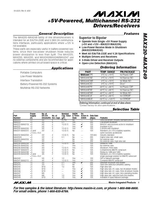
General DescriptionThe MAX220–MAX249 family of line drivers/receivers is intended for all EIA/TIA-232E and V.28/V.24 communica-tions interfaces, particularly applications where ±12V is not available.These parts are especially useful in battery-powered sys-tems, since their low-power shutdown mode reduces power dissipation to less than 5µW. The MAX225,MAX233, MAX235, and MAX245/MAX246/MAX247 use no external components and are recommended for appli-cations where printed circuit board space is critical.________________________ApplicationsPortable Computers Low-Power Modems Interface TranslationBattery-Powered RS-232 Systems Multidrop RS-232 Networks____________________________Features Superior to Bipolaro Operate from Single +5V Power Supply (+5V and +12V—MAX231/MAX239)o Low-Power Receive Mode in Shutdown (MAX223/MAX242)o Meet All EIA/TIA-232E and V.28 Specifications o Multiple Drivers and Receiverso 3-State Driver and Receiver Outputs o Open-Line Detection (MAX243)Ordering InformationOrdering Information continued at end of data sheet.*Contact factory for dice specifications.MAX220–MAX249+5V-Powered, Multichannel RS-232Drivers/Receivers________________________________________________________________Maxim Integrated Products 1Selection Table19-4323; Rev 9; 4/00Power No. of NominalSHDN RxPart Supply RS-232No. of Cap. Value & Three-Active in Data Rate Number (V)Drivers/Rx Ext. Caps (µF)State SHDN (kbps)FeaturesMAX220+52/24 4.7/10No —120Ultra-low-power, industry-standard pinout MAX222+52/2 4 0.1Yes —200Low-power shutdownMAX223 (MAX213)+54/54 1.0 (0.1)Yes ✔120MAX241 and receivers active in shutdown MAX225+55/50—Yes ✔120Available in SOMAX230 (MAX200)+55/04 1.0 (0.1)Yes —120 5 drivers with shutdownMAX231 (MAX201)+5 and2/2 2 1.0 (0.1)No —120Standard +5/+12V or battery supplies; +7.5 to +13.2same functions as MAX232MAX232 (MAX202)+52/24 1.0 (0.1)No —120 (64)Industry standardMAX232A+52/240.1No —200Higher slew rate, small caps MAX233 (MAX203)+52/20— No —120No external capsMAX233A+52/20—No —200No external caps, high slew rate MAX234 (MAX204)+54/04 1.0 (0.1)No —120Replaces 1488MAX235 (MAX205)+55/50—Yes —120No external capsMAX236 (MAX206)+54/34 1.0 (0.1)Yes —120Shutdown, three stateMAX237 (MAX207)+55/34 1.0 (0.1)No —120Complements IBM PC serial port MAX238 (MAX208)+54/44 1.0 (0.1)No —120Replaces 1488 and 1489MAX239 (MAX209)+5 and3/52 1.0 (0.1)No —120Standard +5/+12V or battery supplies;+7.5 to +13.2single-package solution for IBM PC serial port MAX240+55/54 1.0Yes —120DIP or flatpack package MAX241 (MAX211)+54/54 1.0 (0.1)Yes —120Complete IBM PC serial port MAX242+52/240.1Yes ✔200Separate shutdown and enableMAX243+52/240.1No —200Open-line detection simplifies cabling MAX244+58/104 1.0No —120High slew rateMAX245+58/100—Yes ✔120High slew rate, int. caps, two shutdown modes MAX246+58/100—Yes ✔120High slew rate, int. caps, three shutdown modes MAX247+58/90—Yes ✔120High slew rate, int. caps, nine operating modes MAX248+58/84 1.0Yes ✔120High slew rate, selective half-chip enables MAX249+56/1041.0Yes✔120Available in quad flatpack packageFor free samples & the latest literature: , or phone 1-800-998-8800.For small orders, phone 1-800-835-8769.M A X 220–M A X 249+5V-Powered, Multichannel RS-232Drivers/ReceiversABSOLUTE MAXIMUM RATINGS—MAX220/222/232A/233A/242/243ELECTRICAL CHARACTERISTICS—MAX220/222/232A/233A/242/243(V CC = +5V ±10%, C1–C4 = 0.1µF‚ MAX220, C1 = 0.047µF, C2–C4 = 0.33µF, T A = T MIN to T MAX ‚ unless otherwise noted.)Note 1:Input voltage measured with T OUT in high-impedance state, SHDN or V CC = 0V.Note 2:For the MAX220, V+ and V- can have a maximum magnitude of 7V, but their absolute difference cannot exceed 13V.Stresses beyond those listed under “Absolute Maximum Ratings” may cause permanent damage to the device. These are stress ratings only, and functional operation of the device at these or any other conditions beyond those indicated in the operational sections of the specifications is not implied. Exposure to absolute maximum rating conditions for extended periods may affect device reliability.Supply Voltage (V CC )...............................................-0.3V to +6V Input VoltagesT IN ..............................................................-0.3V to (V CC - 0.3V)R IN (Except MAX220)........................................................±30V R IN (MAX220).....................................................................±25V T OUT (Except MAX220) (Note 1).......................................±15V T OUT (MAX220)...............................................................±13.2V Output VoltagesT OUT ...................................................................................±15V R OUT .........................................................-0.3V to (V CC + 0.3V)Driver/Receiver Output Short Circuited to GND.........Continuous Continuous Power Dissipation (T A = +70°C)16-Pin Plastic DIP (derate 10.53mW/°C above +70°C)....842mW 18-Pin Plastic DIP (derate 11.11mW/°C above +70°C)....889mW20-Pin Plastic DIP (derate 8.00mW/°C above +70°C)..440mW 16-Pin Narrow SO (derate 8.70mW/°C above +70°C)...696mW 16-Pin Wide SO (derate 9.52mW/°C above +70°C)......762mW 18-Pin Wide SO (derate 9.52mW/°C above +70°C)......762mW 20-Pin Wide SO (derate 10.00mW/°C above +70°C)....800mW 20-Pin SSOP (derate 8.00mW/°C above +70°C)..........640mW 16-Pin CERDIP (derate 10.00mW/°C above +70°C).....800mW 18-Pin CERDIP (derate 10.53mW/°C above +70°C).....842mW Operating Temperature RangesMAX2_ _AC_ _, MAX2_ _C_ _.............................0°C to +70°C MAX2_ _AE_ _, MAX2_ _E_ _..........................-40°C to +85°C MAX2_ _AM_ _, MAX2_ _M_ _.......................-55°C to +125°C Storage Temperature Range.............................-65°C to +160°C Lead Temperature (soldering, 10sec).............................+300°CMAX220–MAX249+5V-Powered, Multichannel RS-232Drivers/Receivers_______________________________________________________________________________________3Note 3:MAX243 R2OUT is guaranteed to be low when R2IN is ≥0V or is floating.ELECTRICAL CHARACTERISTICS—MAX220/222/232A/233A/242/243 (continued)(V= +5V ±10%, C1–C4 = 0.1µF‚ MAX220, C1 = 0.047µF, C2–C4 = 0.33µF, T = T to T ‚ unless otherwise noted.)M A X 220–M A X 249+5V-Powered, Multichannel RS-232Drivers/Receivers 4_________________________________________________________________________________________________________________________________Typical Operating CharacteristicsMAX220/MAX222/MAX232A/MAX233A/MAX242/MAX243108-1051525OUTPUT VOLTAGE vs. LOAD CURRENT-4-6-8-2642LOAD CURRENT (mA)O U T P U T V O L T A G E (V )1002011104104060AVAILABLE OUTPUT CURRENTvs. DATA RATE65798DATA RATE (kbits/sec)O U T P U T C U R R E N T (m A )203050+10V-10VMAX222/MAX242ON-TIME EXITING SHUTDOWN+5V +5V 0V0V 500µs/div V +, V - V O L T A G E (V )MAX220–MAX249+5V-Powered, Multichannel RS-232Drivers/Receivers_______________________________________________________________________________________5V CC ...........................................................................-0.3V to +6V V+................................................................(V CC - 0.3V) to +14V V-............................................................................+0.3V to -14V Input VoltagesT IN ............................................................-0.3V to (V CC + 0.3V)R IN ......................................................................................±30V Output VoltagesT OUT ...................................................(V+ + 0.3V) to (V- - 0.3V)R OUT .........................................................-0.3V to (V CC + 0.3V)Short-Circuit Duration, T OUT ......................................Continuous Continuous Power Dissipation (T A = +70°C)14-Pin Plastic DIP (derate 10.00mW/°C above +70°C)....800mW 16-Pin Plastic DIP (derate 10.53mW/°C above +70°C)....842mW 20-Pin Plastic DIP (derate 11.11mW/°C above +70°C)....889mW 24-Pin Narrow Plastic DIP(derate 13.33mW/°C above +70°C)..........1.07W24-Pin Plastic DIP (derate 9.09mW/°C above +70°C)......500mW 16-Pin Wide SO (derate 9.52mW/°C above +70°C).........762mW20-Pin Wide SO (derate 10 00mW/°C above +70°C).......800mW 24-Pin Wide SO (derate 11.76mW/°C above +70°C).......941mW 28-Pin Wide SO (derate 12.50mW/°C above +70°C) .............1W 44-Pin Plastic FP (derate 11.11mW/°C above +70°C).....889mW 14-Pin CERDIP (derate 9.09mW/°C above +70°C)..........727mW 16-Pin CERDIP (derate 10.00mW/°C above +70°C)........800mW 20-Pin CERDIP (derate 11.11mW/°C above +70°C)........889mW 24-Pin Narrow CERDIP(derate 12.50mW/°C above +70°C)..............1W24-Pin Sidebraze (derate 20.0mW/°C above +70°C)..........1.6W 28-Pin SSOP (derate 9.52mW/°C above +70°C).............762mW Operating Temperature RangesMAX2 _ _ C _ _......................................................0°C to +70°C MAX2 _ _ E _ _...................................................-40°C to +85°C MAX2 _ _ M _ _ ...............................................-55°C to +125°C Storage Temperature Range.............................-65°C to +160°C Lead Temperature (soldering, 10sec).............................+300°CABSOLUTE MAXIMUM RATINGS—MAX223/MAX230–MAX241ELECTRICAL CHARACTERISTICS—MAX223/MAX230–MAX241(MAX223/230/232/234/236/237/238/240/241, V CC = +5V ±10; MAX233/MAX235, V CC = 5V ±5%‚ C1–C4 = 1.0µF; MAX231/MAX239,V CC = 5V ±10%; V+ = 7.5V to 13.2V; T A = T MIN to T MAX ; unless otherwise noted.)Stresses beyond those listed under “Absolute Maximum Ratings” may cause permanent damage to the device. These are stress ratings only, and functional operation of the device at these or any other conditions beyond those indicated in the operational sections of the specifications is not implied. Exposure to absolute maximum rating conditions for extended periods may affect device reliability.M A X 220–M A X 249+5V-Powered, Multichannel RS-232Drivers/Receivers 6_______________________________________________________________________________________ELECTRICAL CHARACTERISTICS—MAX223/MAX230–MAX241 (continued)(MAX223/230/232/234/236/237/238/240/241, V CC = +5V ±10; MAX233/MAX235, V CC = 5V ±5%‚ C1–C4 = 1.0µF; MAX231/MAX239,V CC = 5V ±10%; V+ = 7.5V to 13.2V; T A = T MIN to T MAX ; unless otherwise noted.)MAX220–MAX249+5V-Powered, Multichannel RS-232Drivers/Receivers_______________________________________________________________________________________78.56.54.55.5TRANSMITTER OUTPUT VOLTAGE (V OH ) vs. V CC7.08.0V CC (V)V O H (V )5.07.57.46.02500TRANSMITTER OUTPUT VOLTAGE (V OH )vs. LOAD CAPACITANCE AT DIFFERENT DATA RATES6.46.27.27.0LOAD CAPACITANCE (pF)V O H (V )1500100050020006.86.612.04.02500TRANSMITTER SLEW RATE vs. LOAD CAPACITANCE6.05.011.09.010.0LOAD CAPACITANCE (pF)S L E W R A T E (V /µs )1500100050020008.07.0-6.0-9.04.55.5TRANSMITTER OUTPUT VOLTAGE (V OL ) vs. V CC-8.0-8.5-6.5-7.0V CC (V)V O L (V )5.0-7.5-6.0-7.62500TRANSMITTER OUTPUT VOLTAGE (V OL )vs. LOAD CAPACITANCE AT DIFFERENT DATA RATES-7.0-7.2-7.4-6.2-6.4LOAD CAPACITANCE (pF)V O L (V )150010005002000-6.6-6.810-105101520253035404550TRANSMITTER OUTPUT VOLTAGE (V+, V-)vs. LOAD CURRENT-2-6-4-886CURRENT (mA)V +, V - (V )420__________________________________________Typical Operating CharacteristicsMAX223/MAX230–MAX241*SHUTDOWN POLARITY IS REVERSED FOR NON MAX241 PARTSV+, V- WHEN EXITING SHUTDOWN(1µF CAPACITORS)MAX220-13SHDN*V-O V+500ms/divM A X 220–M A X 249+5V-Powered, Multichannel RS-232Drivers/Receivers 8_______________________________________________________________________________________ABSOLUTE MAXIMUM RATINGS—MAX225/MAX244–MAX249ELECTRICAL CHARACTERISTICS—MAX225/MAX244–MAX249(MAX225, V CC = 5.0V ±5%; MAX244–MAX249, V CC = +5.0V ±10%, external capacitors C1–C4 = 1µF; T A = T MIN to T MAX ; unless oth-erwise noted.)Note 4:Input voltage measured with transmitter output in a high-impedance state, shutdown, or V CC = 0V.Stresses beyond those listed under “Absolute Maximum Ratings” may cause permanent damage to the device. These are stress ratings only, and functional operation of the device at these or any other conditions beyond those indicated in the operational sections of the specifications is not implied. Exposure to absolute maximum rating conditions for extended periods may affect device reliability.Supply Voltage (V CC )...............................................-0.3V to +6V Input VoltagesT IN ‚ ENA , ENB , ENR , ENT , ENRA ,ENRB , ENTA , ENTB ..................................-0.3V to (V CC + 0.3V)R IN .....................................................................................±25V T OUT (Note 3).....................................................................±15V R OUT ........................................................-0.3V to (V CC + 0.3V)Short Circuit (one output at a time)T OUT to GND............................................................Continuous R OUT to GND............................................................ContinuousContinuous Power Dissipation (T A = +70°C)28-Pin Wide SO (derate 12.50mW/°C above +70°C).............1W 40-Pin Plastic DIP (derate 11.11mW/°C above +70°C)...611mW 44-Pin PLCC (derate 13.33mW/°C above +70°C)...........1.07W Operating Temperature RangesMAX225C_ _, MAX24_C_ _ ..................................0°C to +70°C MAX225E_ _, MAX24_E_ _ ...............................-40°C to +85°C Storage Temperature Range.............................-65°C to +160°C Lead Temperature (soldering,10sec)..............................+300°CMAX220–MAX249+5V-Powered, Multichannel RS-232Drivers/Receivers_______________________________________________________________________________________9Note 5:The 300Ωminimum specification complies with EIA/TIA-232E, but the actual resistance when in shutdown mode or V CC =0V is 10M Ωas is implied by the leakage specification.ELECTRICAL CHARACTERISTICS—MAX225/MAX244–MAX249 (continued)(MAX225, V CC = 5.0V ±5%; MAX244–MAX249, V CC = +5.0V ±10%, external capacitors C1–C4 = 1µF; T A = T MIN to T MAX ; unless oth-erwise noted.)M A X 220–M A X 249+5V-Powered, Multichannel RS-232Drivers/Receivers 10________________________________________________________________________________________________________________________________Typical Operating CharacteristicsMAX225/MAX244–MAX24918212345TRANSMITTER SLEW RATE vs. LOAD CAPACITANCE86416LOAD CAPACITANCE (nF)T R A N S M I T T E R S L E W R A T E (V /µs )14121010-105101520253035OUTPUT VOLTAGEvs. LOAD CURRENT FOR V+ AND V--2-4-6-88LOAD CURRENT (mA)O U T P U T V O L T A G E (V )64209.05.012345TRANSMITTER OUTPUT VOLTAGE (V+, V-)vs. LOAD CAPACITANCE AT DIFFERENT DATA RATES6.05.58.5LOAD CAPACITANCE (nF)V +, V (V )8.07.57.06.5MAX220–MAX249Drivers/Receivers______________________________________________________________________________________11Figure 1. Transmitter Propagation-Delay Timing Figure 2. Receiver Propagation-Delay TimingFigure 3. Receiver-Output Enable and Disable Timing Figure 4. Transmitter-Output Disable TimingM A X 220–M A X 249Drivers/Receivers 12______________________________________________________________________________________ENT ENR OPERATION STATUS TRANSMITTERSRECEIVERS00Normal Operation All Active All Active 01Normal Operation All Active All 3-State10Shutdown All 3-State All Low-Power Receive Mode 11ShutdownAll 3-StateAll 3-StateTable 1a. MAX245 Control Pin ConfigurationsENT ENR OPERATION STATUS TRANSMITTERS RECEIVERSTA1–TA4TB1–TB4RA1–RA5RB1–RB500Normal Operation All Active All Active All Active All Active 01Normal Operation All Active All Active RA1–RA4 3-State,RA5 Active RB1–RB4 3-State,RB5 Active 1ShutdownAll 3-StateAll 3-StateAll Low-Power Receive Mode All Low-Power Receive Mode 11Shutdown All 3-State All 3-StateRA1–RA4 3-State,RA5 Low-Power Receive ModeRB1–RB4 3-State,RB5 Low-Power Receive ModeTable 1b. MAX245 Control Pin ConfigurationsTable 1c. MAX246 Control Pin ConfigurationsENA ENB OPERATION STATUS TRANSMITTERS RECEIVERSTA1–TA4TB1–TB4RA1–RA5RB1–RB500Normal Operation All Active All Active All Active All Active 01Normal Operation All Active All 3-State All Active RB1–RB4 3-State,RB5 Active 1ShutdownAll 3-StateAll ActiveRA1–RA4 3-State,RA5 Active All Active 11Shutdown All 3-State All 3-StateRA1–RA4 3-State,RA5 Low-Power Receive ModeRB1–RB4 3-State,RA5 Low-Power Receive ModeMAX220–MAX249Drivers/Receivers______________________________________________________________________________________13Table 1d. MAX247/MAX248/MAX249 Control Pin ConfigurationsM A X 220–M A X 249_______________Detailed DescriptionThe MAX220–MAX249 contain four sections: dual charge-pump DC-DC voltage converters, RS-232 dri-vers, RS-232 receivers, and receiver and transmitter enable control inputs.Dual Charge-Pump Voltage ConverterThe MAX220–MAX249 have two internal charge-pumps that convert +5V to ±10V (unloaded) for RS-232 driver operation. The first converter uses capacitor C1 to dou-ble the +5V input to +10V on C3 at the V+ output. The second converter uses capacitor C2 to invert +10V to -10V on C4 at the V- output.A small amount of power may be drawn from the +10V (V+) and -10V (V-) outputs to power external circuitry (see the Typical Operating Characteristics section),except on the MAX225 and MAX245–MAX247, where these pins are not available. V+ and V- are not regulated,so the output voltage drops with increasing load current.Do not load V+ and V- to a point that violates the mini-mum ±5V EIA/TIA-232E driver output voltage when sourcing current from V+ and V- to external circuitry. When using the shutdown feature in the MAX222,MAX225, MAX230, MAX235, MAX236, MAX240,MAX241, and MAX245–MAX249, avoid using V+ and V-to power external circuitry. When these parts are shut down, V- falls to 0V, and V+ falls to +5V. For applica-tions where a +10V external supply is applied to the V+pin (instead of using the internal charge pump to gen-erate +10V), the C1 capacitor must not be installed and the SHDN pin must be tied to V CC . This is because V+is internally connected to V CC in shutdown mode.RS-232 DriversThe typical driver output voltage swing is ±8V when loaded with a nominal 5k ΩRS-232 receiver and V CC =+5V. Output swing is guaranteed to meet the EIA/TIA-232E and V.28 specification, which calls for ±5V mini-mum driver output levels under worst-case conditions.These include a minimum 3k Ωload, V CC = +4.5V, and maximum operating temperature. Unloaded driver out-put voltage ranges from (V+ -1.3V) to (V- +0.5V). Input thresholds are both TTL and CMOS compatible.The inputs of unused drivers can be left unconnected since 400k Ωinput pull-up resistors to V CC are built in (except for the MAX220). The pull-up resistors force the outputs of unused drivers low because all drivers invert.The internal input pull-up resistors typically source 12µA,except in shutdown mode where the pull-ups are dis-abled. Driver outputs turn off and enter a high-imped-ance state—where leakage current is typically microamperes (maximum 25µA)—when in shutdownmode, in three-state mode, or when device power is removed. Outputs can be driven to ±15V. The power-supply current typically drops to 8µA in shutdown mode.The MAX220 does not have pull-up resistors to force the ouputs of the unused drivers low. Connect unused inputs to GND or V CC .The MAX239 has a receiver three-state control line, and the MAX223, MAX225, MAX235, MAX236, MAX240,and MAX241 have both a receiver three-state control line and a low-power shutdown control. Table 2 shows the effects of the shutdown control and receiver three-state control on the receiver outputs.The receiver TTL/CMOS outputs are in a high-imped-ance, three-state mode whenever the three-state enable line is high (for the MAX225/MAX235/MAX236/MAX239–MAX241), and are also high-impedance whenever the shutdown control line is high.When in low-power shutdown mode, the driver outputs are turned off and their leakage current is less than 1µA with the driver output pulled to ground. The driver output leakage remains less than 1µA, even if the transmitter output is backdriven between 0V and (V CC + 6V). Below -0.5V, the transmitter is diode clamped to ground with 1k Ωseries impedance. The transmitter is also zener clamped to approximately V CC + 6V, with a series impedance of 1k Ω.The driver output slew rate is limited to less than 30V/µs as required by the EIA/TIA-232E and V.28 specifica-tions. Typical slew rates are 24V/µs unloaded and 10V/µs loaded with 3Ωand 2500pF.RS-232 ReceiversEIA/TIA-232E and V.28 specifications define a voltage level greater than 3V as a logic 0, so all receivers invert.Input thresholds are set at 0.8V and 2.4V, so receivers respond to TTL level inputs as well as EIA/TIA-232E and V.28 levels.The receiver inputs withstand an input overvoltage up to ±25V and provide input terminating resistors withDrivers/Receivers 14Table 2. Three-State Control of ReceiversMAX220–MAX249Drivers/Receivers______________________________________________________________________________________15nominal 5k Ωvalues. The receivers implement Type 1interpretation of the fault conditions of V.28 and EIA/TIA-232E.The receiver input hysteresis is typically 0.5V with a guaranteed minimum of 0.2V. This produces clear out-put transitions with slow-moving input signals, even with moderate amounts of noise and ringing. The receiver propagation delay is typically 600ns and is independent of input swing direction.Low-Power Receive ModeThe low-power receive-mode feature of the MAX223,MAX242, and MAX245–MAX249 puts the IC into shut-down mode but still allows it to receive information. This is important for applications where systems are periodi-cally awakened to look for activity. Using low-power receive mode, the system can still receive a signal that will activate it on command and prepare it for communi-cation at faster data rates. This operation conserves system power.Negative Threshold—MAX243The MAX243 is pin compatible with the MAX232A, differ-ing only in that RS-232 cable fault protection is removed on one of the two receiver inputs. This means that control lines such as CTS and RTS can either be driven or left floating without interrupting communication. Different cables are not needed to interface with different pieces of equipment.The input threshold of the receiver without cable fault protection is -0.8V rather than +1.4V. Its output goes positive only if the input is connected to a control line that is actively driven negative. If not driven, it defaults to the 0 or “OK to send” state. Normally‚ the MAX243’s other receiver (+1.4V threshold) is used for the data line (TD or RD)‚ while the negative threshold receiver is con-nected to the control line (DTR‚ DTS‚ CTS‚ RTS, etc.). Other members of the RS-232 family implement the optional cable fault protection as specified by EIA/TIA-232E specifications. This means a receiver output goes high whenever its input is driven negative‚ left floating‚or shorted to ground. The high output tells the serial communications IC to stop sending data. To avoid this‚the control lines must either be driven or connected with jumpers to an appropriate positive voltage level.Shutdown—MAX222–MAX242On the MAX222‚ MAX235‚ MAX236‚ MAX240‚ and MAX241‚ all receivers are disabled during shutdown.On the MAX223 and MAX242‚ two receivers continue to operate in a reduced power mode when the chip is in shutdown. Under these conditions‚ the propagation delay increases to about 2.5µs for a high-to-low input transition. When in shutdown, the receiver acts as a CMOS inverter with no hysteresis. The MAX223 and MAX242 also have a receiver output enable input (EN for the MAX242 and EN for the MAX223) that allows receiver output control independent of SHDN (SHDN for MAX241). With all other devices‚ SHDN (SH DN for MAX241) also disables the receiver outputs.The MAX225 provides five transmitters and five receivers‚ while the MAX245 provides ten receivers and eight transmitters. Both devices have separate receiver and transmitter-enable controls. The charge pumps turn off and the devices shut down when a logic high is applied to the ENT input. In this state, the supply cur-rent drops to less than 25µA and the receivers continue to operate in a low-power receive mode. Driver outputs enter a high-impedance state (three-state mode). On the MAX225‚ all five receivers are controlled by the ENR input. On the MAX245‚ eight of the receiver out-puts are controlled by the ENR input‚ while the remain-ing two receivers (RA5 and RB5) are always active.RA1–RA4 and RB1–RB4 are put in a three-state mode when ENR is a logic high.Receiver and Transmitter EnableControl InputsThe MAX225 and MAX245–MAX249 feature transmitter and receiver enable controls.The receivers have three modes of operation: full-speed receive (normal active)‚ three-state (disabled)‚ and low-power receive (enabled receivers continue to function at lower data rates). The receiver enable inputs control the full-speed receive and three-state modes. The transmitters have two modes of operation: full-speed transmit (normal active) and three-state (disabled). The transmitter enable inputs also control the shutdown mode. The device enters shutdown mode when all transmitters are disabled. Enabled receivers function in the low-power receive mode when in shutdown.M A X 220–M A X 249Tables 1a–1d define the control states. The MAX244has no control pins and is not included in these tables. The MAX246 has ten receivers and eight drivers with two control pins, each controlling one side of the device. A logic high at the A-side control input (ENA )causes the four A-side receivers and drivers to go into a three-state mode. Similarly, the B-side control input (ENB ) causes the four B-side drivers and receivers to go into a three-state mode. As in the MAX245, one A-side and one B-side receiver (RA5 and RB5) remain active at all times. The entire device is put into shut-down mode when both the A and B sides are disabled (ENA = ENB = +5V).The MAX247 provides nine receivers and eight drivers with four control pins. The ENRA and ENRB receiver enable inputs each control four receiver outputs. The ENTA and ENTB transmitter enable inputs each control four drivers. The ninth receiver (RB5) is always active.The device enters shutdown mode with a logic high on both ENTA and ENTB .The MAX248 provides eight receivers and eight drivers with four control pins. The ENRA and ENRB receiver enable inputs each control four receiver outputs. The ENTA and ENTB transmitter enable inputs control four drivers each. This part does not have an always-active receiver. The device enters shutdown mode and trans-mitters go into a three-state mode with a logic high on both ENTA and ENTB .The MAX249 provides ten receivers and six drivers with four control pins. The ENRA and ENRB receiver enable inputs each control five receiver outputs. The ENTA and ENTB transmitter enable inputs control three dri-vers each. There is no always-active receiver. The device enters shutdown mode and transmitters go into a three-state mode with a logic high on both ENTA and ENTB . In shutdown mode, active receivers operate in a low-power receive mode at data rates up to 20kbits/sec.__________Applications InformationFigures 5 through 25 show pin configurations and typi-cal operating circuits. In applications that are sensitive to power-supply noise, V CC should be decoupled to ground with a capacitor of the same value as C1 and C2 connected as close as possible to the device.Drivers/Receivers16______________________________________________________________________________________。

新品发布NEW PRODUCTS今日电子 · 2018年5月 · 外带来新的层面,例如,混光。
整合式M O S F E T额定60V,使A L8862成为可行的解决方案,可用于更高功率的输出应用。
利用Diodes公司的专有技术,M O S F E T也具备仅0.4Ω的超低R D S(O N),能在缩减外部零件需求的同时展现出高效率。
亦针对短路或开路可能造成的故障情形提供完整保护,同时包含了过热保护。
Diodes Incorporated线性LED控制器A L5814、A L5817、A L5815及AL5816线性LED控制器,为LED灯条提供可调光和可调节的驱动电流,效率高达80%以上。
A L58x x系列提供物料列表(B O M)成本低廉的解决方案,适用于商业和工业领域的各项产品应用,包括广告牌、仪器照明、家电内部照明、建筑细部照明,以及一般智能照明设备。
这些装置的输入范围为4.5~60V,无须电感,可保持良好的E M I效能,使系统整合更简单。
此外,相较于其他设计,外部功率晶体管可使内部功耗降至最低。
A L58x x系列可提供高达15m A 的电流给外部MOSFET或双极晶体管,以驱动LED灯条。
LED驱动电流由一个外部电阻配置,具有4%的参考电压准确度,以及出色的温度稳定性。
不仅如此,AL5815与AL5816装置支持PWM调光功能,A L5814与A L5817装置则同时支持模拟和PWM调光功能。
保护功能包括过温保护及输入欠压锁定。
A L5814及A L5817装置也利用VFAULT脚位提供「LED 开回路」保护功能,以及L E D 热回流保护。
A L58x x系列线性控制器提供良好的E M I效能,而广泛的工作温度范围(-40~+105℃)使其适用于恶劣环境。
Diodes Incorporated超小电源模块MAXM17532和MAXM15462超小尺寸(2.6mm×3.0mm×1.5mm)、集成式DC-DC电源模块是Maxim喜马拉雅电源方案专有组合的一部分,适用于工业、医疗健康、通信和消费市场。

General DescriptionThe MAX3070E–MAX3079E 3.3V, ±15kV ESD-protected,RS-485/RS-422 transceivers feature one driver and one receiver. These devices include fail-safe circuitry, guar-anteeing a logic-high receiver output when receiver inputs are open or shorted. The receiver outputs a logic high if all transmitters on a terminated bus are disabled (high impedance). The MAX3070E–MAX3079E include a hot-swap capability to eliminate false transitions on the bus during power-up or hot insertion.The MAX3070E/MAX3071E/MAX3072E feature reduced slew-rate drivers that minimize EMI and reduce reflec-tions caused by improperly terminated cables, allowing error-free data transmission up to 250kbps. The MAX3073E/MAX3074E/MAX3075E also feature slew-rate-limited drivers but allow transmit speeds up to 500kbps. The MAX3076E/MAX3077E/MAX3078E driver slew rates are not limited, making transmit speeds up to 16Mbps possible. The MAX3079E slew rate is pin selectable for 250kbps, 500kbps, and 16Mbps.The MAX3072E/MAX3075E/MAX3078E are intended for half-duplex communications, and the MAX3070E/MAX3071E/MAX3073E/MAX3074E/MAX3076E/MAX3077E are intended for full-duplex communications. The MAX3079E is selectable for half-duplex or full-duplex operation. It also features independently programmable receiver and transmitter output phase through separate pins.The MAX3070E–MAX3079E transceivers draw 800µA of supply current when unloaded or when fully loaded with the drivers disabled. All devices have a 1/8-unit load receiver input impedance, allowing up to 256transceivers on the bus.ApplicationsLighting Systems Industrial Control Telecom Security Systems InstrumentationFeatureso 3.3V Operationo Electrostatic Discharge (ESD) Protection for RS-485 I/O Pins±15kV Human Body Model o True Fail-Safe Receiver While Maintaining EIA/TIA-485 Compatibility o Hot-Swap Input Structure on DE and RE o Enhanced Slew-Rate Limiting Facilitates Error-Free Data Transmission(MAX3070E–MAX3075E/MAX3079E)o Low-Current Shutdown Mode (Except MAX3071E/MAX3074E/MAX3077E)o Pin-Selectable Full-/Half-Duplex Operation (MAX3079E)o Phase Controls to Correct for Twisted-Pair Reversal (MAX3079E)o Allow Up to 256 Transceivers on the Bus o Available in Industry-Standard 8-Pin SO PackageMAX3070E–MAX3079E+3.3V , ±15kV ESD-Protected, Fail-Safe, Hot-Swap, RS-485/RS-422 Transceivers________________________________________________________________Maxim Integrated Products 1Ordering Information19-2668; Rev 1; 1/03For pricing, delivery, and ordering information,please contact Maxim/Dallas Direct!at 1-888-629-4642, or visit Maxim’s website at .Selector Guide, Pin Configurations, and Typical Operating Circuits appear at end of data sheet.Ordering Information continued at end of data sheet.M A X 3070E –M A X 3079E+3.3V , ±15kV ESD-Protected, Fail-Safe, Hot-Swap, RS-485/RS-422 Transceivers 2_______________________________________________________________________________________ABSOLUTE MAXIMUM RATINGSDC ELECTRICAL CHARACTERISTICSStresses beyond those listed under “Absolute Maximum Ratings” may cause permanent damage to the device. These are stress ratings only, and functional operation of the device at these or any other conditions beyond those indicated in the operational sections of the specifications is not implied. Exposure to absolute maximum rating conditions for extended periods may affect device reliability.(All voltages referenced to GND)Supply Voltage (V CC ).............................................................+6V Control Input Voltage (RE , DE, SLR,H/F , TXP, RXP)......................................................-0.3V to +6V Driver Input Voltage (DI)...........................................-0.3V to +6V Driver Output Voltage (Z, Y, A, B).............................-8V to +13V Receiver Input Voltage (A, B)....................................-8V to +13V Receiver Input VoltageFull Duplex (A, B)..................................................-8V to +13V Receiver Output Voltage (RO)....................-0.3V to (V CC + 0.3V)Driver Output Current.....................................................±250mAContinuous Power Dissipation (T A = +70°C)8-Pin SO (derate 5.88mW/°C above +70°C).................471mW 8-Pin Plastic DIP (derate 9.09mW/°C above +70°C).....727mW 14-Pin SO (derate 8.33mW/°C above +70°C)...............667mW 14-Pin Plastic DIP (derate 10.0mW/°C above +70°C)...800mW Operating Temperature RangesMAX307_EE_ _................................................-40°C to +85°C MAX307_EA_ _..............................................-40°C to +125°C Junction Temperature......................................................+150°C Storage Temperature Range.............................-65°C to +150°C Lead Temperature (soldering, 10s).................................+300°CMAX3070E–MAX3079E+3.3V , ±15kV ESD-Protected, Fail-Safe, Hot-Swap, RS-485/RS-422 Transceivers_______________________________________________________________________________________3DC ELECTRICAL CHARACTERISTICS (continued)Note 1:All currents into the device are positive. All currents out of the device are negative. All voltages are referred to deviceground, unless otherwise noted.Note 2:∆V OD and ∆V OC are the changes in V OD and V OC , respectively, when the DI input changes state.Note 3:The short-circuit output current applies to peak current just prior to foldback current limiting. The short-circuit foldback out-put current applies during current limiting to allow a recovery from bus contention.M A X 3070E –M A X 3079E+3.3V , ±15kV ESD-Protected, Fail-Safe, Hot-Swap, RS-485/RS-422 Transceivers 4_______________________________________________________________________________________DRIVER SWITCHING CHARACTERISTICSMAX3070E/MAX3071E/MAX3072E/MAX3079E with SRL = UNCONNECTED (250kbps)RECEIVER SWITCHING CHARACTERISTICSMAX3070E/MAX3071E/MAX3072E/MAX3079E with SRL = UNCONNECTED (250kbps)(V CC = 3.3V ±10%, T A = T MIN to T MAX , unless otherwise noted. Typical values are at V CC = 3.3V and T A = +25°C.)MAX3070E–MAX3079E+3.3V , ±15kV ESD-Protected, Fail-Safe, Hot-Swap, RS-485/RS-422 Transceivers_______________________________________________________________________________________5DRIVER SWITCHING CHARACTERISTICSMAX3073E/MAX3074E/MAX3075E/MAX3079E with SRL = V CC (500kbps)RECEIVER SWITCHING CHARACTERISTICSMAX3073E/MAX3074E/MAX3075E/MAX3079E with SRL = V CC (500kbps)M A X 3070E –M A X 3079E+3.3V , ±15kV ESD-Protected, Fail-Safe, Hot-Swap, RS-485/RS-422 Transceivers 6_______________________________________________________________________________________DRIVER SWITCHING CHARACTERISTICSMAX3076E/MAX3077E/MAX3078E/MAX3079E with SRL = GND (16Mbps)RECEIVER SWITCHING CHARACTERISTICSMAX3076E/MAX3077E/MAX3078E/MAX3079E with SRL = GND (16Mbps)MAX3070E–MAX3079E+3.3V , ±15kV ESD-Protected, Fail-Safe, Hot-Swap, RS-485/RS-422 Transceivers_______________________________________________________________________________________7SUPPLY CURRENT vs. TEMPERATURETEMPERATURE (°C)S U P P L Y C U R R E N T (m A )100755025-250.60.70.80.91.00.5-50125OUTPUT CURRENTvs. RECEIVER OUTPUT HIGH VOLTAGEM A X 3070E t o c 02OUTPUT HIGH VOLTAGE (V)O U T P U T C U R R E N T (m A )3.02.52.01.51.00.55101520253000 3.5OUTPUT CURRENTvs. RECEIVER OUTPUT LOW VOLTAGEM A X 3070E t o c 03OUTPUT HIGH VOLTAGE (V)O U T P U T C U R R E N T (m A )3.02.52.01.51.00.551015202530350 3.5RECEIVER OUTPUT HIGH VOLTAGEvs. TEMPERATURETEMPERATURE (°C)O U T P U T H I G H V O L T A G E (V )100755025-253.053.103.153.203.253.303.00-50125RECEIVER OUTPUT LOW VOLTAGEvs. TEMPERATURETEMPERATURE (°C)O U T P U T L O W V O L T A G E (V )10075-25025500.10.20.30.40.50.60.70.8-50125DRIVER OUTPUT CURRENTvs. DIFFERENTIAL OUTPUT VOLTAGEM A X 3070E t o c 06DIFFERENTIAL OUTPUT VOLTAGE (V)O U T P U T C U R R E N T (m A )3.02.51.5 2.01.00.51020304050607080901000 3.5DRIVER DIFFERENTIAL OUTPUT VOLTAGEvs. TEMPERATURETEMPERATURE (°C)D I F FE R E N T I A L O U T P U T V O L T A G E (V )100752550-251.701.801.902.002.102.202.302.402.502.601.60-50125OUTPUT CURRENTvs. TRANSMITTER OUTPUT HIGH VOLTAGEOUTPUT HIGH VOLTAGE (V)O U T P U T C U R R E N T (m A )32-6-5-4-2-10-31204060801001201401600-74OUTPUT CURRENTvs. TRANSMITTER OUTPUT LOW VOLTAGEOUTPUT LOW VOLTAGE (V)O U T P U T C U R R E N T (m A )10864220406080100120140160180012Typical Operating Characteristics(V CC = 3.3V, T A = +25°C, unless otherwise noted.)M A X 3070E –M A X 3079E+3.3V , ±15kV ESD-Protected, Fail-Safe, Hot-Swap, RS-485/RS-422 Transceivers 8_______________________________________________________________________________________SHUTDOWN CURRENT vs. TEMPERATURETEMPERATURE (°C)S H U T D O W N C U R R E N T (µA )100752550-250.20.40.60.81.01.21.41.61.82.00-50125DRIVER PROPAGATION DELAY vs. TEMPERATURE (250kbps)TEMPERATURE (°C)D R I VE R P R O P A G A T I O N D E L A Y (n s )100755025-256007008009001000500-50125DRIVER PROPAGATION DELAY vs. TEMPERATURE (500kbps)TEMPERATURE (°C)D R I V ER P R O P A G A T I O N D E L A Y (n s )100755025-25250300350400450500200-50125DRIVER PROPAGATION DELAY vs. TEMPERATURE (16Mbps)TEMPERATURE (°C)D R I VE R P R O P A G A T I O N D E L A Y (n s )100755025-25510152025300-50125RECEIVER PROPAGATION DELAYvs. TEMPERATURE (250kbps AND 500kbps)TEMPERATURE (°C)D R IV E R P R O P A G A T I O N D E L A Y (n s )100755025-253060901201500-50125RECEIVER PROPAGATION DELAY vs. TEMPERATURE (16Mbps)TEMPERATURE (°C)R E C E I V E R P R O P A G A T I O N D E L A Y (n s )1007550250-25102030405060700-50125DRIVER PROPAGATION DELAY (250kbps)MAX3070E toc161µs/div V Y - V Z 2V/div DI 2V/divRECEIVER PROPAGATION DELAY(250kbps AND 500kbps)MAX3070E toc17200ns/divV A - V B 1V/divRO 2V/divTypical Operating Characteristics (continued)(V CC = 3.3V, T A = +25°C, unless otherwise noted.)MAX3070E–MAX3079E+3.3V , ±15kV ESD-Protected, Fail-Safe, Hot-Swap, RS-485/RS-422 Transceivers_______________________________________________________________________________________9Test Circuits and WaveformsDRIVER PROPAGATION DELAY (500kbps)MAX3070E toc18400ns/div V Y - V Z 2V/divDI 2V/divDRIVER PROPAGATION DELAY (16Mbps)MAX3070E toc1910ns/div V Z 1V/divV Y 1V/divDI 2V/divRECEIVER PROPAGATION DELAY (16Mbps)MAX3070E toc2020ns/divV A 1V/divV B 1V/divRO 2V/divTypical Operating Characteristics (continued)(V CC = 3.3V, T A = +25°C, unless otherwise noted.)Figure 2. Driver Timing Test CircuitFigure 3. Driver Propagation DelaysM A X 3070E –M A X 3079E+3.3V , ±15kV ESD-Protected, Fail-Safe, Hot-Swap, RS-485/RS-422 Transceivers 10______________________________________________________________________________________Test Circuits and Waveforms (continued)DHZ DZH DZH(SHDN)Figure 5. Driver Enable and Disable Times (t DZL , t DLZ , t DLZ(SHDN))MAX3070E–MAX3079E+3.3V , ±15kV ESD-Protected, Fail-Safe, Hot-Swap, RS-485/RS-422 TransceiversTest Circuits and Waveforms (continued)Figure 6. Receiver Propagation Delay Test CircuitFigure 8. Receiver Enable and Disable TimesM A X 3070E –M A X 3079E+3.3V , ±15kV ESD-Protected, Fail-Safe, Hot-Swap, RS-485/RS-422 TransceiversMAX3070E–MAX3079E+3.3V , ±15kV ESD-Protected, Fail-Safe, Hot-Swap, RS-485/RS-422 TransceiversMAX3070E/MAX3073E/MAX3076EPin Description (continued)MAX3071E/MAX3074E/MAX30767EFunction TablesM A X 3070E –M A X 3079E+3.3V , ±15kV ESD-Protected, Fail-Safe, Hot-Swap, RS-485/RS-422 Transceivers MAX3072E/MAX3075E/MAX3078EFunction Tables (continued)MAX3079EDetailed Description The MAX3070E–MAX3079E high-speed transceivers for RS-485/RS-422 communication contain one driver and one receiver. These devices feature fail-safe circuitry, which guarantees a logic-high receiver output when the receiver inputs are open or shorted, or when they are connected to a terminated transmission line with all dri-vers disabled (see the Fail-Safe section). The MAX3070E/MAX3072E/MAX3073E/MAX3075E/ MAX3076E/MAX3078E/MAX3079E also feature a hot-swap capability allowing line insertion without erro-neous data transfer (see the Hot Swap Capability section). The MAX3070E/MAX3071E/MAX3072E feature reduced slew-rate drivers that minimize EMI and reduce reflections caused by improperly terminated cables, allowing error-free data transmission up to 250kbps. The MAX3073E/MAX3074E/MAX3075E also offer slew-rate limits allowing transmit speeds up to 500kbps. The MAX3076E/MAX3077E/MAX3078Es’ dri-ver slew rates are not limited, making transmit speeds up to 16Mbps possible. The MAX3079E’s slew rate is selectable between 250kbps, 500kbps, and 16Mbps by driving a selector pin with a three-state driver.The MAX3072E/MAX3075E/MAX3078E are half-duplex transceivers, while the MAX3070E/MAX3071E/ MAX3073E/MAX3074E/MAX3076E/MAX3077E are full-duplex transceivers. The MAX3079E is selectable between half- and full-duplex communication by driving a selector pin (SRL) high or low, respectively.All devices operate from a single 3.3V supply. Drivers are output short-circuit current limited. Thermal-shutdown cir-cuitry protects drivers against excessive power dissipa-tion. When activated, the thermal-shutdown circuitry places the driver outputs into a high-impedance state.Receiver Input Filtering The receivers of the MAX3070E–MAX3075E, and the MAX3079E when operating in 250kbps or 500kbps mode, incorporate input filtering in addition to input hysteresis. This filtering enhances noise immunity with differential signals that have very slow rise and fall times. Receiver propagation delay increases by 25% due to this filtering.Fail-Safe The MAX3070E family guarantees a logic-high receiver output when the receiver inputs are shorted or open, or when they are connected to a terminated transmission line with all drivers disabled. This is done by setting the receiver input threshold between -50mV and -200mV. If the differential receiver input voltage (A - B) is greater than or equal to -50mV, RO is logic high. If A - B is less than or equal to -200mV, RO is logic low. In the case ofa terminated bus with all transmitters disabled, the receiver’s differential input voltage is pulled to 0V bythe termination. With the receiver thresholds of theMAX3070E family, this results in a logic high with a50mV minimum noise margin. Unlike previous fail-safe devices, the -50mV to -200mV threshold complies withthe ±200mV EIA/TIA-485 standard.Hot-Swap Capability (Except MAX3071E/MAX3074E/MAX3077E)Hot-Swap InputsWhen circuit boards are inserted into a hot, or pow-ered, backplane, differential disturbances to the databus can lead to data errors. Upon initial circuit board insertion, the data communication processor under-goes its own power-up sequence. During this period,the processor’s logic-output drivers are high imped-ance and are unable to drive the DE and RE inputs ofthese devices to a defined logic level. Leakage cur-rents up to ±10µA from the high-impedance state of the processor’s logic drivers could cause standard CMOS enable inputs of a transceiver to drift to an incorrectlogic level. Additionally, parasitic circuit board capaci-tance could cause coupling of V CC or GND to the enable inputs. Without the hot-swap capability, these factors could improperly enable the transceiver’s driveror receiver.When V CC rises, an internal pulldown circuit holds DElow and RE high. After the initial power-up sequence,the pulldown circuit becomes transparent, resetting thehot-swap tolerable input.Hot-Swap Input CircuitryThe enable inputs feature hot-swap capability. At theinput there are two NMOS devices, M1 and M2 (Figure 9). When V CC ramps from zero, an internal 10µstimer turns on M2 and sets the SR latch, which alsoturns on M1. Transistors M2, a 500µA current sink, andM1, a 100µA current sink, pull DE to GND through a5kΩresistor. M2 is designed to pull DE to the disabledstate against an external parasitic capacitance up to100pF that can drive DE high. After 10µs, the timer deactivates M2 while M1 remains on, holding DE low against three-state leakages that can drive DE high. M1 remains on until an external source overcomes the required input current. At this time, the SR latch resetsand M1 turns off. When M1 turns off, DE reverts to a standard, high-impedance CMOS input. Whenever V CCdrops below 1V, the hot-swap input is reset.For RE there is a complementary circuit employing two PMOS devices pulling RE to V CC.MAX3070E–MAX3079E+3.3V, ±15kV ESD-Protected, Fail-Safe, Hot-Swap, RS-485/RS-422 TransceiversM A X 3070E –M A X 3079EMAX3079E ProgrammingThe MAX3079E has several programmable operating modes. Transmitter rise and fall times are programma-ble, resulting in maximum data rates of 250kbps,500kbps, and 16Mbps. To select the desired data rate,drive SRL to one of three possible states by using a three-state driver: V CC , GND, or unconnected. F or 250kbps operation, set the three-state device in high-impedance mode or leave SRL unconnected. F or 500kbps operation, drive SRL high or connect it to V CC .F or 16Mbps operation, drive SRL low or connect it to GND. SRL can be changed during operation without interrupting data communications.Occasionally, twisted-pair lines are connected backward from normal orientation. The MAX3079E has two pins that invert the phase of the driver and the receiver to correct this problem. F or normal operation, drive TXP and RXP low, connect them to ground, or leave them unconnect-ed (internal pulldown). To invert the driver phase, drive TXP high or connect it to V CC . To invert the receiver phase, drive RXP high or connect it to V CC . Note that the receiver threshold is positive when RXP is high.The MAX3079E can operate in full- or half-duplex mode. Drive the H/F pin low, leave it unconnected (internal pulldown), or connect it to GND for full-duplexoperation. Drive H/F high for half-duplex operation. In full-duplex mode, the pin configuration of the driver and receiver is the same as that of a MAX3070E. In half-duplex mode, the receiver inputs are switched to the driver outputs, connecting outputs Y and Z to inputs A and B, respectively. In half-duplex mode, the internal full-duplex receiver input resistors are still connected to pins 11 and 12.±15kV ESD ProtectionAs with all Maxim devices, ESD-protection structures are incorporated on all pins to protect against electro-static discharges encountered during handling and assembly. The driver outputs and receiver inputs of the MAX3070E family of devices have extra protection against static electricity. Maxim ’s engineers have devel-oped state-of-the-art structures to protect these pins against ESD of ±15kV without damage. The ESD struc-tures withstand high ESD in all states: normal operation,shutdown, and powered down. After an ESD event, the MAX3070E –MAX3079E keep working without latchup or damage.ESD protection can be tested in various ways. The transmitter outputs and receiver inputs of the MAX3070E –MAX3079E are characterized for protection to the following limits:•±15kV using the Human Body Model•±6kV using the Contact Discharge method specified in IEC 1000-4-2ESD Test ConditionsESD performance depends on a variety of conditions.Contact Maxim for a reliability report that documents test setup, test methodology, and test results.Human Body ModelFigure 10a shows the Human Body Model, and Figure 10b shows the current waveform it generates when dis-charged into a low impedance. This model consists of a 100pF capacitor charged to the ESD voltage of interest,which is then discharged into the test device through a 1.5k Ωresistor.IEC 1000-4-2The IEC 1000-4-2 standard covers ESD testing and performance of finished equipment. However, it does not specifically refer to integrated circuits. The MAX3070E family of devices helps you design equip-ment to meet IEC 1000-4-2, without the need for addi-tional ESD-protection components.The major difference between tests done using the Human Body Model and IEC 1000-4-2 is higher peak+3.3V , ±15kV ESD-Protected, Fail-Safe, Hot-Swap, RS-485/RS-422 Transceiverscurrent in IEC 1000-4-2, because series resistance is lower in the IEC 1000-4-2 model. Hence, the ESD with-stand voltage measured to IEC 1000-4-2 is generally lower than that measured using the Human Body Model.F igure 10c shows the IEC 1000-4-2 model, and F igure 10d shows the current waveform for IEC 1000-4-2 ESD Contact Discharge test.The air-gap test involves approaching the device with a charged probe. The contact-discharge method connects the probe to the device before the probe is energized.Machine Model The machine model for ESD tests all pins using a 200pF storage capacitor and zero discharge resis-tance. The objective is to emulate the stress caused when I/O pins are contacted by handling equipment during test and assembly. Of course, all pins require this protection, not just RS-485 inputs and outputs.Applications Information256 Transceivers on the BusThe standard RS-485 receiver input impedance is 12kΩ(1-unit load), and the standard driver can drive up to 32-unit loads. The MAX3070E family of transceivers has a1/8-unit load receiver input impedance (96kΩ), allowingup to 256 transceivers to be connected in parallel on one communication line. Any combination of these devicesas well as other RS-485 transceivers with a total of 32-unit loads or fewer can be connected to the line.Reduced EMI and ReflectionsThe MAX3070E/MAX3071E/MAX3072E feature reducedslew-rate drivers that minimize EMI and reduce reflec-tions caused by improperly terminated cables, allowingerror-free data transmission up to 250kbps. TheMAX3073E/MAX3074E/MAX3075E offer higher driver output slew-rate limits, allowing transmit speeds up to500kbps. The MAX3079E with SRL = V CC or uncon-nected, are slew-rate limited. With SRL unconnected,the MAX3079E error-free data transmission is up to250kbps; with SRL connected to V CC the data transmit speeds up to 500kbps.MAX3070E–MAX3079E+3.3V, ±15kV ESD-Protected, Fail-Safe, Hot-Swap, RS-485/RS-422 TransceiversM A X 3070E –M A X 3079ELow-Power Shutdown Mode (Except MAX3071E/MAX3074E/MAX3077E)Low-power shutdown mode is initiated by bringing both RE high and DE low. In shutdown, the devices typically draw only 50nA of supply current.RE and DE can be driven simultaneously; the parts are guaranteed not to enter shutdown if RE is high and DE is low for less than 50ns. If the inputs are in this state for at least 600ns, the parts are guaranteed to enter shutdown.Enable times t ZH and t ZL (see the Switching Characteristics section) assume the part was not in a low-power shutdown state. Enable times t ZH(SHDN)and t ZL(SHDN)assume the parts were shut down. It takes drivers and receivers longer to become enabled from low-power shutdown mode (t ZH(SHDN), t ZL(SHDN)) than from driver/receiver-disable mode (t ZH , t ZL ).Driver Output ProtectionTwo mechanisms prevent excessive output current and power dissipation caused by faults or by bus contention.The first, a foldback current limit on the output stage,provides immediate protection against short circuits over the whole common-mode voltage range (see the Typical Operating Characteristics ). The second, a thermal-shut-down circuit, forces the driver outputs into a high-imped-ance state if the die temperature becomes excessive.Line LengthThe RS-485/RS-422 standard covers line lengths up to 4000ft. F or line lengths greater than 4000ft, use the repeater application shown in Figure 11.Typical ApplicationsThe MAX3072E/MAX3075E/MAX3078E/MAX3079E transceivers are designed for bidirectional data commu-nications on multipoint bus transmission lines. F igures 12 and 13 show typical network applications circuits. To minimize reflections, terminate the line at both ends in its characteristic impedance, and keep stub lengths off the main line as short as possible. The slew-rate-lim-ited MAX3072E/MAX3075E and the two modes of the MAX3079E are more tolerant of imperfect termination.Chip InformationTRANSISTOR COUNT: 1228PROCESS: BiCMOS+3.3V , ±15kV ESD-Protected, Fail-Safe, Hot-Swap, RS-485/RS-422 TransceiversFigure 11. Line Repeater for MAX3070E/MAX3071E/MAX3073E/MAX3074E/MAX3076E/MAX3077E/MAX3079E in Full-Duplex Mode+3.3V, ±15kV ESD-Protected, Fail-Safe, Hot-Swap, RS-485/RS-422 TransceiversMAX3070E–MAX3079EM A X 3070E –M A X 3079E+3.3V , ±15kV ESD-Protected, Fail-Safe, Hot-Swap, RS-485/RS-422 TransceiversPin Configurations and Typical Operating CircuitsMAX3070E–MAX3079E+3.3V , ±15kV ESD-Protected, Fail-Safe, Hot-Swap, RS-485/RS-422 Transceivers______________________________________________________________________________________21Pin Configurations and Typical Operating Circuits (continued)M A X 3070E –M A X 3079E+3.3V , ±15kV ESD-Protected, Fail-Safe, Hot-Swap, RS-485/RS-422 Transceivers 22______________________________________________________________________________________Ordering Information (continued)MAX3070E–MAX3079E+3.3V , ±15kV ESD-Protected, Fail-Safe, Hot-Swap, RS-485/RS-422 Transceivers______________________________________________________________________________________23Package Information(The package drawing(s) in this data sheet may not reflect the most current specifications. For the latest package outline information,go to /packages .)M A X 3070E –M A X 3079E+3.3V , ±15kV ESD-Protected, Fail-Safe, Hot-Swap, RS-485/RS-422 Transceivers 24______________________________________________________________________________________Package Information (continued)(The package drawing(s) in this data sheet may not reflect the most current specifications. For the latest package outline information,go to /packages .)MAX3070E–MAX3079E+3.3V , ±15kV ESD-Protected, Fail-Safe, Hot-Swap, RS-485/RS-422 TransceiversMaxim cannot assume responsibility for use of any circuitry other than circuitry entirely embodied in a Maxim product. N o circuit patent licenses are implied. Maxim reserves the right to change the circuitry and specifications without notice at any time.Maxim Integrated Products, 120 San Gabriel Drive, Sunnyvale, CA 94086 408-737-7600 ____________________25©2003 Maxim Integrated ProductsPrinted USAis a registered trademark of Maxim Integrated Products.Package Information (continued)(The package drawing(s) in this data sheet may not reflect the most current specifications. For the latest package outline information,go to /packages .)。


General DescriptionThe MAX1277/MAX1279 are low-power, high-speed, seri-al-output, 12-bit, analog-to-digital converters (ADCs) with an internal reference that operates at up to 1.5Msps.These devices feature true-differential inputs, offering bet-ter noise immunity, distortion improvements, and a wider dynamic range over single-ended inputs. A standard SPI™/QSPI™/MICROWIRE™interface provides the clock necessary for conversion. These devices easily interface with standard digital signal processor (DSP) synchronous serial interfaces.The MAX1277/MAX1279 operate from a single +2.7V to +3.6V supply voltage. The MAX1277/MAX1279 include a 2.048V internal reference. The MAX1277 has a unipolar analog input, while the MAX1279 has a bipolar analog input. These devices feature a partial power-down mode and a full power-down mode for use between conver-sions, which lower the supply current to 2mA (typ) and 1µA (max), respectively. Also featured is a separate power-supply input (V L ), which allows direct interfacing to +1.8V to V DD digital logic. The fast conversion speed,low-power dissipation, excellent AC performance, and DC accuracy (±1 LSB INL) make the MAX1277/MAX1279ideal for industrial process control, motor control, and base-station applications.The MAX1277/MAX1279 come in a 12-pin TQFN pack-age, and are available in the commercial (0°C to +70°C)and extended (-40°C to +85°C) temperature ranges.ApplicationsData Acquisition Communications Bill Validation Portable InstrumentsMotor ControlFeatures♦1.5Msps Sampling Rate♦Only 22mW (typ) Power Dissipation ♦Only 1µA (max) Shutdown Current♦High-Speed, SPI-Compatible, 3-Wire Serial Interface ♦68.5dB S/(N + D) at 525kHz Input Frequency ♦Internal True-Differential Track/Hold (T/H)♦Internal 2.048V Reference ♦No Pipeline Delays♦Small 12-Pin TQFN PackageMAX1277/MAX12791.5Msps, Single-Supply, Low-Power, True-Differential, 12-Bit ADCs with Internal Reference________________________________________________________________Maxim Integrated Products119-3365; Rev 0; 8/04For pricing, delivery, and ordering information,please contact Maxim/Dallas Direct!at 1-888-629-4642, or visit Maxim’s website at .SPI/QSPI are trademarks of Motorola, Inc.MICROWIRE is a trademark of National Semiconductor Corp.M A X 1277/M A X 12791.5Msps, Single-Supply, Low-Power, True-Differential, 12-Bit ADCs with Internal ReferenceABSOLUTE MAXIMUM RATINGSELECTRICAL CHARACTERISTICSStresses beyond those listed under “Absolute Maximum Ratings” may cause permanent damage to the device. These are stress ratings only, and functional operation of the device at these or any other conditions beyond those indicated in the operational sections of the specifications is not implied. Exposure to absolute maximum rating conditions for extended periods may affect device reliability.V DD to GND..............................................................-0.3V to +6V V L to GND................-0.3V to the lower of (V DD + 0.3V) and +6V Digital Inputsto GND.................-0.3V to the lower of (V DD + 0.3V) and +6V Digital Outputto GND....................-0.3V to the lower of (V L + 0.3V) and +6V Analog Inputs andREF to GND..........-0.3V to the lower of (V DD + 0.3V) and +6V RGND to GND.......................................................-0.3V to +0.3VMaximum Current into Any Pin............................................50mA Continuous Power Dissipation (T A = +70°C)12-Pin TQFN (derate 16.9mW/°C above +70°C)......1349mW Operating Temperature RangesMAX127_ _ CTC.................................................0°C to +70°C MAX127_ _ ETC..............................................-40°C to +85°C Junction Temperature......................................................+150°C Storage Temperature Range.............................-60°C to +150°C Lead Temperature (soldering, 10s).................................+300°CMAX1277/MAX12791.5Msps, Single-Supply, Low-Power, True-Differential, 12-Bit ADCs with Internal Reference_______________________________________________________________________________________3ELECTRICAL CHARACTERISTICS (continued)(V DD = +2.7V to +3.6V, V L = V DD , f SCLK = 24MHz, 50% duty cycle, T A = T MIN to T MAX , unless otherwise noted. Typical values are at T A = +25°C.)M A X 1277/M A X 12791.5Msps, Single-Supply, Low-Power, True-Differential, 12-Bit ADCs with Internal Reference 4_______________________________________________________________________________________Note 1:Relative accuracy is the deviation of the analog value at any code from its theoretical value after the gain error and the offseterror have been nulled.Note 2:No missing codes over temperature.Note 3:Conversion time is defined as the number of clock cycles (16) multiplied by the clock period.Note 4:At sample rates below 10ksps, the input full-linear bandwidth is reduced to 5kHz.Note 5:The listed value of three SCLK cycles is given for full-speed continuous conversions. Acquisition time begins on the 14th ris-ing edge of SCLK and terminates on the next falling edge of CNVST. The IC idles in acquisition mode between conversions.Note 6:Undersampling at the maximum signal bandwidth requires the minimum jitter spec for SINAD performance.Note 7:1.5Msps operation guaranteed for V L > 2.7V. See the Typical Operating Characteristics section for recommended samplingspeeds for V L < 2.7V.Note 8:Digital supply current is measured with the V IH level equal to V L , and the V IL level equal to GND.TIMING CHARACTERISTICSFigure 1. Detailed Serial-Interface Timing Figure 2. Load Circuits for Enable/Disable TimesMAX1277/MAX12791.5Msps, Single-Supply, Low-Power, True-Differential, 12-Bit ADCs with Internal Reference_______________________________________________________________________________________5Typical Operating Characteristics(V DD = +3V, V L = V DD , f SCLK = 24MHz, f SAMPLE = 1.5Msps, T A = T MIN to T MAX , unless otherwise noted. Typical values are measured at T A = +25°C.)MAXIMUM RECOMMENDED f SCLK vs. V LM A X 1277/79 t o c 01V L (V)f S C L K (M H z )3.33.02.72.42.119212325171.83.6-1.00-0.75-0.50-0.2500.250.500.751.0001024204830724096INTEGRAL NONLINEARITYvs. DIGITAL OUTPUT CODE (MAX1277)M A X 1277/79 t o c 02DIGITAL OUTPUT CODEI N L (L S B )-1.00-0.75-0.50-0.2500.250.500.751.00-2048-1024010242048INTEGRAL NONLINEARITYvs. DIGITAL OUTPUT CODE (MAX1279)M A X 1277/79 t o c 03DIGITAL OUTPUT CODEI N L (L S B )-1.00-0.75-0.50-0.2500.250.500.751.0001024204830724096DIFFERENTIAL NONLINEARITY vs. DIGITAL OUTPUT CODE (MAX1277)M A X 1277/79 t o c 04DIGITAL OUTPUT CODE D N L (L S B )-1.00-0.75-0.50-0.2500.250.500.751.00-2048-1024010242048DIFFERENTIAL NONLINEARITY vs. DIGITAL OUTPUT CODE (MAX1279)M A X 1277/79 t o c 05DIGITAL OUTPUT CODE D N L (L S B )-6-4-5-2-3-10-4010-15356085OFFSET ERRORvs. TEMPERATURE (MAX1277)M A X 1277/79 t o c 06TEMPERATURE (°C)O F F S E T E R R O R (L S B )-6-4-5-2-3-10-4010-15356085OFFSET ERRORvs. TEMPERATURE (MAX1279)M A X 1277/79 t o c 07TEMPERATURE (°C)O F F S E T E R R O R (L S B )-20-12134-4010-15356085GAIN ERRORvs. TEMPERATURE (MAX1277)M A X 1277/79 t o c 08TEMPERATURE (°C)G A I N E R R O R (L S B )-4-2-30-112-4010-15356085GAIN ERRORvs. TEMPERATURE (MAX1279)M A X 1277/79 t o c 09TEMPERATURE (°C)G A I N E R R O R (L S B )Typical Operating Characteristics (continued)(V DD = +3V, V L = V DD , f SCLK = 24MHz, f SAMPLE = 1.5Msps, T A = T MIN to T MAX , unless otherwise noted. Typical values are measured at T A = +25°C.)M A X 1277/M A X 12791.5Msps, Single-Supply, Low-Power, True-Differential, 12-Bit ADCs with Internal Reference 6_______________________________________________________________________________________70.069.569.068.568.0100300200400500DYNAMIC PERFORMANCE vs. INPUT FREQUENCY (MAX1277)ANALOG INPUT FREQUENCY (kHz)D Y N A M I C PE RF O R M A N C E (d B )70.069.569.068.568.0100300200400500DYNAMIC PERFORMANCEvs. INPUT FREQUENCY (MAX1279)ANALOG INPUT FREQUENCY (kHz)D Y N A M I C PE RF O R M A N C E (d B )-80-84-88-92-96100300200400500THD vs. INPUT FREQUENCYANALOG INPUT FREQUENCY (kHz)T H D (d B )828488869092SFDR vs. INPUT FREQUENCYANALOG INPUT FREQUENCY (kHz)S F D R (d B )100300200400500-140-100-120-60-80-20-4000250375125500625750FFT PLOT (MAX1277)ANALOG INPUT FREQUENCY (kHz)A M P L I T U D E (d B )f IN = 500kHz SINAD = 68.7dB SNR = 68.9dB THD = -83.1dB SFDR = 85.0dB-140-100-120-60-80-20-4000250375125500625750FFT PLOT (MAX1279)ANALOG INPUT FREQUENCY (kHz)A M P L I T U D E (dB )f IN = 500kHz SINAD = 69.0dB SNR = 69.1dB THD = -88.9dB SFDR = 85.9dBMAX1277/MAX12791.5Msps, Single-Supply, Low-Power, True-Differential, 12-Bit ADCs with Internal Reference_______________________________________________________________________________________7TOTAL HARMONIC DISTORTION vs. SOURCE IMPEDANCESOURCE IMPEDANCE (Ω)T H D (d B )100-90-80-70-60-50-100101000TWO-TONE IMD PLOT (MAX1277)ANALOG INPUT FREQUENCY (kHz)A M P L I T U D E (dB )625500375250125-120-100-80-60-40-200-140750TWO-TONE IMD PLOT (MAX1279)ANALOG INPUT FREQUENCY (kHz)A M P L I T U D E (dB )625500375250125-120-100-80-60-40-200-1407500.200.600.400.801.00-4010-15356085V DD /V L FULL POWER-DOWNSUPPLY CURRENT vs. TEMPERATURETEMPERATURE (°C)V D D /V L S U P P L Y C U R R E N T (µA )0502575100-4010-15356085V L PARTIAL/FULL POWER-DOWN SUPPLY CURRENT vs. TEMPERATURETEMPERATURE (°C)V L S U P P L Y C U R R E N T (µA )03.01.56.04.57.59.0-4010-15356085V DD SUPPLY CURRENT vs. TEMPERATURETEMPERATURE (°C)V D D S U P P L Y C U R R E N T (m A )Typical Operating Characteristics (continued)(V DD = +3V, V L = V DD , f SCLK = 24MHz, f SAMPLE = 1.5Msps, T A = T MIN to T MAX , unless otherwise noted. Typical values are measured at T A = +25°C.)M A X 1277/M A X 12791.5Msps, Single-Supply, Low-Power, True-Differential, 12-Bit ADCs with Internal Reference 8_______________________________________________________________________________________Typical Operating Characteristics (continued)(V DD = +3V, V L = V DD , f SCLK = 24MHz, f SAMPLE = 1.5Msps, T A = T MIN to T MAX , unless otherwise noted. Typical values are measured at T A = +25°C.)864200750250500100012501500V DD SUPPLY CURRENT vs. CONVERSION RATEM A X 1277/79 t o c 22f SAMPLE (kHz)V D D S U P P L Y C U R R E N T (m A )00.100.300.200.400.50-4010-15356085V L SUPPLY CURRENT vs. TEMPERATURETEMPERATURE (°C)V L S U P P L Y C U R R E N T (m A )0501501002002500500250750100012501500V L SUPPLY CURRENT vs. CONVERSION RATEf SAMPLE (kHz)V L S U P P L Y C U R R E N T (µA )2.002.022.012.042.032.052.06-4010-15356085REFERENCE VOLTAGE vs. TEMPERATUREM A X 1277/79 t o c 25TEMPERATURE (°C)R E F E R E N C E V O L T A G E (V )2.052.042.032.022.014268REFERENCE VOLTAGE vs. LOAD CURRENT (SOURCE)M A X 1277/79 t o c 26LOAD CURRENT (mA)R E F E R E N C E V O L T A G E (V )2.082.072.062.052.0410050150200REFERENCE VOLTAGE vs. LOAD CURRENT (SINK)M A X 1277/79 t o c 27LOAD CURRENT (µA)R E F E R E N C E V O L T A G E (V )MAX1277/MAX12791.5Msps, Single-Supply, Low-Power, True-Differential, 12-Bit ADCs with Internal ReferencePin DescriptionM A X 1277/M A X 1279True-Differential Analog Input T/HThe equivalent circuit of Figure 4 shows the input archi-tecture of the MAX1277/MAX1279, which is composed of a T/H, a comparator, and a switched-capacitor digi-tal-to-analog converter (DAC). The T/H enters its track-ing mode on the 14th SCLK rising edge of the previous conversion. Upon power-up, the T/H enters its tracking mode immediately. The positive input capacitor is con-nected to AIN+. The negative input capacitor is con-nected to AIN-. The T/H enters its hold mode on the falling edge of CNVST and the difference between the sampled positive and negative input voltages is convert-ed. The time required for the T/H to acquire an input sig-nal is determined by how quickly its input capacitance is charged. If the input signal’s source impedance is high,the acquisition time lengthens. The acquisition time,t ACQ , is the minimum time needed for the signal to be acquired. It is calculated by the following equation:t ACQ ≥9 ×(RS + R IN ) ×16pFwhere R IN = 200Ω, and RS is the source impedance of the input signal.Note:t ACQ is never less than 125ns and any source impedance below 12Ωdoes not significantly affect the ADC’s AC performance.Input BandwidthThe ADC’s input-tracking circuitry has a 15MHz small-signal bandwidth, making it possible to digitize high-speed transient events and measure periodic signals with bandwidths exceeding the ADC’s sampling rate by using undersampling techniques. To avoid high-frequency signals being aliased into the frequency band of interest, anti-alias filtering is recommended.Analog Input ProtectionInternal protection diodes that clamp the analog input to V DD and GND allow the analog input pins to swing from GND - 0.3V to V DD + 0.3V without damage. Both inputs must not exceed V DD or be lower than GND for accurate conversions.Serial InterfaceInitialization After Power-Up and Starting a ConversionUpon initial power-up, the MAX1277/MAX1279 require a complete conversion cycle to initialize the internal cali-bration. Following this initial conversion, the part is ready for normal operation. This initialization is only required after a hardware power-up sequence and is not required after exiting partial or full power-down mode.To start a conversion, pull CNVST low. At CNVST’s falling edge, the T/H enters its hold mode and a conver-sion is initiated. SCLK runs the conversion and the data can then be shifted out serially on DOUT.1.5Msps, Single-Supply, Low-Power, True-Differential, 12-Bit ADCs with Internal Reference10______________________________________________________________________________________Figure 6. SPI Interface—Partial Power-Down ModeFigure 5. Interface-Timing SequenceTiming and ControlConversion-start and data-read operations are con-trolled by the CNVST and SCLK digital inputs. Figures 1and 5 show timing diagrams, which outline the serial-interface operation.A CNVST falling edge initiates a conversion sequence;the T/H stage holds the input voltage, the ADC begins to convert, and DOUT changes from high impedance to logic low. SCLK is used to drive the conversion process, and it shifts data out as each bit of the conver-sion is determined.SCLK begins shifting out the data after the 4th rising edge of SCLK. DOUT transitions t DOUT after each SCLK’s rising edge and remains valid 4ns (t DHOLD )after the next rising edge. The 4th rising clock edge produces the MSB of the conversion at DOUT, and the MSB remains valid 4ns after the 5th rising edge. Since there are 12 data bits and 3 leading zeros, at least 16rising clock edges are needed to shift out these bits.For continuous operation, pull CNVST high between the 14th and the 16th SCLK rising edges. If CNVST stays low after the falling edge of the 16th SCLK cycle, the DOUT line goes to a high-impedance state on either CNVST’s rising edge or the next SCLK’s rising edge.Partial Power-Down and Full Power-Down ModesPower consumption can be reduced significantly by plac-ing the MAX1277/MAX1279 in either partial power-down mode or full power-down mode. Partial power-down mode is ideal for infrequent data sampling and fast wake-up time applications. Pull CNVST high after the 3rd SCLK rising edge and before the 14th SCLK rising edge to enter and stay in partial power-down mode (see Figure 6). This reduces the supply current to 2mA. While in par-tial power-down mode, the reference remains enabled to allow valid conversions once the IC is returned to normal mode. Drive CNVST low and allow at least 14 SCLK cycles to elapse before driving CNVST high to exit partial power-down mode.Full power-down mode is ideal for infrequent data sam-pling and very low supply current applications. The MAX1277/MAX1279 have to be in partial power-down mode to enter full power-down mode. Perform the SCLK/CNVST sequence described above to enter par-tial power-down mode. Then repeat the same sequence to enter full power-down mode (see Figure 7). Drive CNVST low, and allow at least 14 SCLK cycles to elapse before driving CNVST high to exit full power-down mode. While in full power-down mode, the refer-ence is disabled to minimize power consumption. Be sure to allow at least 2ms recovery time after exiting full power-down mode for the reference to settle. In partial/full power-down mode, maintain a logic low or a logic high on SCLK to minimize power consumption.Transfer FunctionFigure 8 shows the unipolar transfer function for the MAX1277. Figure 9 shows the bipolar transfer function for the MAX1279. The MAX1277 output is straight binary,while the MAX1279 output is two’s complement.Applications InformationInternal ReferenceThe MAX1277/MAX1279 have an on-chip voltage refer-ence trimmed to 2.048V. The internal reference output is connected to REF and also drives the internal capac-itive DAC. The output can be used as a reference volt-age source for other components and can source up to 2mA. Bypass REF with a 0.01µF capacitor and a 4.7µF capacitor to RGND.The internal reference is continuously powered up dur-ing both normal and partial power-down modes. In full power-down mode, the internal reference is disabled.Be sure to allow at least 2ms recovery time after hard-ware power-up or exiting full power-down mode for the reference to reach its intended value.MAX1277/MAX1279Differential, 12-Bit ADCs with Internal Reference______________________________________________________________________________________11Figure 7. SPI Interface—Full Power-Down ModeM A X 1277/M A X 1279How to Start a ConversionAn analog-to-digital conversion is initiated by CNVST,clocked by SCLK, and the resulting data is clocked out on DOUT by SCLK. With SCLK idling high or low, a falling edge on CNVST begins a conversion. This causes the analog input stage to transition from track to hold mode,and for DOUT to transition from high impedance to being actively driven low. A total of 16 SCLK cycles are required to complete a normal conversion. If CNVST is low during the 16th falling SCLK edge, DOUT returns to high imped-ance on the next rising edge of CNVST or SCLK, enabling the serial interface to be shared by multiple devices. If CNVST returns high after the 14th, but before the 16th SCLK rising edge, DOUT remains active so continuous conversions can be sustained. The highest throughput is achieved when performing continuous conversions. Figure 10 illustrates a conversion using a typical serial interface.Connection toStandard InterfacesThe MAX1277/MAX1279 serial interface is fully compati-ble with SPI/QSPI and MICROWIRE (see Figure 11). If a serial interface is available, set the CPU’s serial interface in master mode so the CPU generates the serial clock.Choose a clock frequency up to 24MHz.SPI and MICROWIREWhen using SPI or MICROWIRE, the MAX1277/ MAX1279are compatible with all four modes programmed with the CPHA and CPOL bits in the SPI or MICROWIRE control register. Conversion begins with a CNVST falling edge.DOUT goes low, indicating a conversion is in progress.Two consecutive 1-byte reads are required to get the full 12 bits from the ADC. DOUT transitions on SCLK rising edges. DOUT is guaranteed to be valid t DOUT later and remains valid until t DHOLD after the following SCLK rising edge. When using CPOL = 0 and CPHA = 0, or CPOL = 1and CPHA = 1, the data is clocked into the µP on the fol-lowing rising edge. When using CPOL = 0 and CPHA = 1,or CPOL = 1 and CPHA = 0, the data is clocked into the µP on the next falling edge. See Figure 11 for connections and Figures 12 and 13 for timing. See the Timing Characteristics section to determine the best mode to use.QSPIUnlike SPI, which requires two 1-byte reads to acquire the 12 bits of data from the ADC, QSPI allows the mini-mum number of clock cycles necessary to clock in the data. The MAX1277/MAX1279 require 16 clock cycles from the µP to clock out the 12 bits of data. Figure 14shows a transfer using CPOL = 1 and CPHA = 1. The conversion result contains three zeros, followed by the 12 data bits, and a trailing zero with the data in MSB-first format.Differential, 12-Bit ADCs with Internal Reference 12______________________________________________________________________________________Figure 8. Unipolar Transfer Function (MAX1277 Only)Figure 9. Bipolar Transfer Function (MAX1279 Only)MAX1277/MAX1279Differential, 12-Bit ADCs with Internal Reference______________________________________________________________________________________13Figure 11. Common Serial-Interface Connections to the MAX1277/MAX1279Figure 10. Continuous Conversion with Burst/Continuous ClockDSP Interface to the TMS320C54_The MAX1277/MAX1279 can be directly connected to the TMS320C54_ family of DSPs from Texas Instruments, Inc. Set the DSP to generate its own clocks or use external clock signals. Use either the standard or buffered serial port. Figure 15 shows the simplest interface between the MAX1277/MAX1279 and the TMS320C54_, where the transmit serial clock (CLKX) drives the receive serial clock (CLKR) and SCLK, and the transmit frame sync (FSX) drives the receive frame sync (FSR) and CNVST.For continuous conversion, set the serial port to trans-mit a clock, and pulse the frame sync signal for a clock period before data transmission. The serial-port config-uration (SPC) register should be set up with internal frame sync (TXM = 1), CLKX driven by an on-chip clock source (MCM = 1), burst mode (FSM = 1), and 16-bit word length (FO = 0).This setup allows continuous conversions provided that the data transmit register (DXR) and the data-receive register (DRR) are serviced before the next conversion.Alternatively, autobuffering can be enabled when using the buffered serial port to execute conversions and read the data without CPU intervention. Connect the V LM A X 1277/M A X 1279Differential, 12-Bit ADCs with Internal Reference 14______________________________________________________________________________________Figure 13. SPI/MICROWIRE Serial-Interface Timing—Continuous Conversion (CPOL = CPHA = 0), (CPOL = CPHA = 1)000D11D10D9D8D7D6D5D4D3D2D1D00DOUT SCLKCNVST111416Figure 12. SPI/MICROWIRE Serial-Interface Timing—Single Conversion (CPOL = CPHA = 0), (CPOL = CPHA = 1)Figure 14. QSPI Serial-Interface Timing—Single Conversion (CPOL = 1, CPHA = 1)MAX1277/MAX1279Differential, 12-Bit ADCs with Internal Reference______________________________________________________________________________________15pin to the TMS320C54_ supply voltage when the MAX1277/MAX1279 are operating with an analog sup-ply voltage higher than the DSP supply voltage. The word length can be set to 8 bits with FO = 1 to imple-ment the power-down modes. The CNVST pin must idle high to remain in either power-down state.Another method of connecting the MAX1277/MAX1279to the TMS320C54_ is to generate the clock signals external to either device. This connection is shown in Figure 16, where serial clock (CLOCK) drives theCLKR, and SCLK and the convert signal (CONVERT)drive the FSR and CNVST.The serial port must be set up to accept an external receive-clock and external receive-frame sync. The SPC register should be written as follows:TXM = 0, external frame syncMCM = 0, CLKX is taken from the CLKX pin FSM = 1, burst modeFO = 0, data transmitted/received as 16-bit wordsThis setup allows continuous conversion, provided that the DRR is serviced before the next conversion.Alternatively, autobuffering can be enabled when using the buffered serial port to read the data without CPU intervention. Connect the V L pin to the TMS320C54_supply voltage when the MAX1277/MAX1279 are oper-ating with an analog supply voltage higher than the DSP supply voltage.The MAX1277/MAX1279 can also be connected to the TMS320C54_ by using the data transmit (DX) pin to drive CNVST and the CLKX generated internally to drive SCLK. A pullup resistor is required on the CNVST signal to keep it high when DX goes high impedance and 0001hex should be written to the DXR continuously for continuous conversions. The power-down modes may be entered by writing 00FFhex to the DXR (see Figures 17 and 18).DSP Interface to the ADSP21_ _ _The MAX1277/MAX1279 can be directly connected to the ADSP21_ _ _ family of DSPs from Analog Devices,Inc. Figure 19 shows the direct connection of the MAX1277/MAX1279 to the ADSP21_ _ _. There are two modes of operation that can be programmed to interface with the MAX1277/MAX1279. For continuous conver-sions, idle CNVST low and pulse it high for one clock cycle during the LSB of the previous transmitted word.The ADSP21_ _ _ STCTL and SRCTL registers should be configured for early framing (LAFR = 0) and for anFigure 15. Interfacing to the TMS320C54_ Internal ClocksFigure 16. Interfacing to the TMS320C54_ External Clocks000D11D10D9D8D7D6D5D4D3D2D1D00DOUT SCLKCNVST0D011Figure 17. DSP Interface—Continuous ConversionM A X 1277/M A X 1279active-high frame (LTFS = 0, LRFS = 0) signal. In this mode, the data-independent frame-sync bit (DITFS = 1)can be selected to eliminate the need for writing to the transmit-data register more than once. For single conver-sions, idle CNVST high and pulse it low for the entire conversion. The ADSP21_ _ _ STCTL and SRCTL regis-ters should be configured for late framing (LAFR = 1)and for an active-low frame (LTFS = 1, LRFS = 1) signal.This is also the best way to enter the power-down modes by setting the word length to 8 bits (SLEN = 1001).Connect the V L pin to the ADSP21_ _ _ supply voltage when the MAX1277/MAX1279 are operating with a sup-ply voltage higher than the DSP supply voltage (see Figures 17 and 18).Layout, Grounding, and BypassingFor best performance, use PC boards. Wire-wrap boards are not recommended. Board layout should ensure that digital and analog signal lines are separat-ed from each other. Do not run analog and digital (especially clock) lines parallel to one another, or digital lines underneath the ADC package.Figure 20 shows the recommended system ground connections. Establish a single-point analog ground (star ground point) at GND, separate from the logic ground. Connect all other analog grounds and DGND to this star ground point for further noise reduction. The ground return to the power supply for this ground should be low impedance and as short as possible for noise-free operation.High-frequency noise in the V DD power supply can affect the ADC’s high-speed comparator. Bypass this supply to the single-point analog ground with 0.01µF and 10µF bypass capacitors. Minimize capacitor lead lengths for best supply-noise rejection.DefinitionsIntegral NonlinearityIntegral nonlinearity (INL) is the deviation of the values on an actual transfer function from a straight line. This straight line can be either a best-straight-line fit or a line drawn between the end points of the transfer function,once offset and gain errors have been nullified. The static linearity parameters for the MAX1277/MAX1279 are mea-sured using the end-points method.Differential, 12-Bit ADCs with Internal Reference 16______________________________________________________________________________________Figure 20. Power-Supply Grounding ConditionFigure 18. DSP Interface—Single-Conversion, Continuous/Burst Clock。