MSP430F42x用户手册
- 格式:pdf
- 大小:1.04 MB
- 文档页数:46
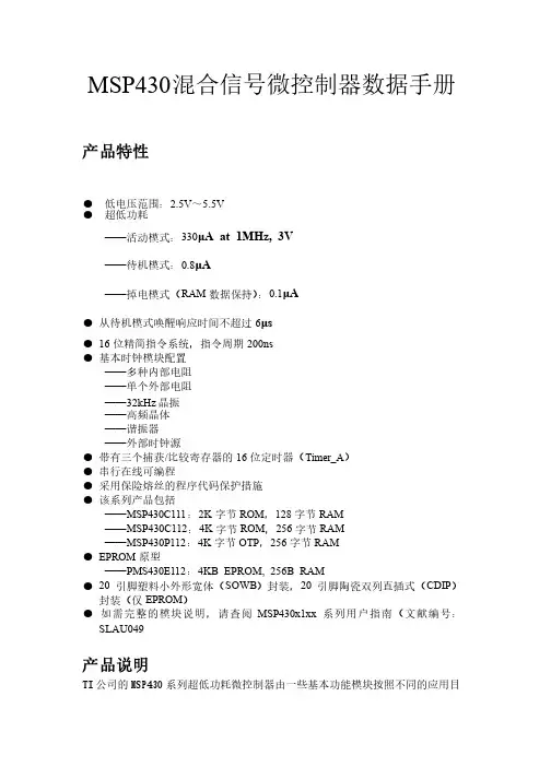
MSP430混合信号微控制器数据手册产品特性●低电压范围:2.5V~5.5V 超低功耗●超低功耗——活动模式:330μA at 1MHz, 3V——待机模式:0.8μA——掉电模式(RAM数据保持):0.1μA ●从待机模式唤醒响应时间不超过6μs ●16位精简指令系统,指令周期200ns ●基本时钟模块配置基本时钟模块配置——多种内部电阻——多种内部电阻——单个外部电阻——单个外部电阻——32kHz晶振晶振——高频晶体——高频晶体——谐振器——谐振器——外部时钟源——外部时钟源●带有三个捕获/比较寄存器的16位定时器(Timer_A)串行在线可编程●串行在线可编程●采用保险熔丝的程序代码保护措施采用保险熔丝的程序代码保护措施该系列产品包括●该系列产品包括——MSP430C111:2K字节ROM,128字节RAM ——MSP430C112:4K字节ROM,256字节RAM ——MSP430P112:4K字节OTP,256字节RAM 原型●EPROM原型——PMS430E112:4KB EPROM, 256B RAM ●20引脚塑料小外形宽体(SOWB)封装,20引脚陶瓷双列直插式(CDIP)封装(仅EPROM)●如需完整的模块说明,请查阅MSP430x1xx系列用户指南(文献编号:SLAU049 产品说明TI公司的MSP43O系列超低功耗微控制器由一些基本功能模块按照不同的应用目标组合而成。
在便携式测量应用中,这种优化的体系结构结合五种低功耗模式可以达到延长电池寿命的目的。
以达到延长电池寿命的目的。
MSP430MSP430系列的CPU 采用16位精简指令系统,集成有16位寄存器和常数发生器,发挥了最高的代码效率。
它采用数字控制振荡器(DCO DCO)),使得从低功耗模式到唤醒模式的转换时间小于6μs.MSP430x11x 系列是一种超低功耗的混合信号微控制器,系列是一种超低功耗的混合信号微控制器,它拥有一个内置的它拥有一个内置的16位计数器和14个I/0引脚。
MSP430F2系列16位超低功耗单片机模块原理第9章定时器B Timer B版本: 1.4日期: 2007.4.原文: TI MSP430x2xxfamily.pdf翻译: 李璘中国计量学院编辑: DC 微控技术论坛版主注:以下文章是翻译TI MSP430x2xxfamily.pdf 文件中的部分内容。
由于我们翻译水平有限,有整理过程中难免有所不足或错误;所以以下内容只供参考.一切以原文为准。
详情请密切留意微控技术论坛。
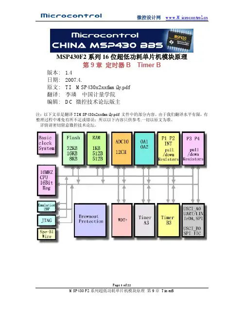
Page 1 of 22定时器B(Timer_B,以后简写为TB)是一个16位的定时/计数器,并复合了捕获/比较寄存器。
Timer_B3(拥有3个捕获比较器)只存在于MSP430x2xx中。
章节9.1 Timer_B 介绍. . . . . . . . . . . . . . . . . . . . . . . . . . . . . . . . . . . . . . . . . . 9-29.2 Timer_B 操作方法. . . . . . . . . . . . . . . . . . . . . . . . . . . . . . . . . . . . . . . . . . . . 9-49.3 Timer_B 寄存器 . . . . . . . . . . . . . . . . . . . . . . . . . . . . . . . . . . . . . . . . . . . 9-199.1 Timer_B 介绍TB是一个16位的定时/计数器,拥有3个或7个捕获/比较寄存器。
TB可以支持捕获/比较功能、PWM输出和定时器功能。
TB还有扩展中断的功能,中断可以由定时器溢出产生或捕获比较寄存器产生。
TB的特性如下:l4种操作模式的异步16位定时/计数器l可选择配置的时钟源l3个或7个可配置的捕获/比较器l可配置的PWM输出l加载时同步的双缓冲比较锁存l对所有TB中断快速响应的中断向量寄存器9.1.1 和定时器A的相同点和不同点定时器B和定时器A的不同点如下:l定时器B的长度是可编程的,可编程为8,10,12,16位l定时器B TBCCRx寄存器是双缓冲的,并可以编组l所有定时器B的输出可以为高阻抗状态l SCCI位功能在定时器B中不存在TB的结构图见图9−1.图9−1.TB结构图Page 2 of 22Page 3 of 229.2 Timer_B 的操作方法TB 模块由用户软件来配置,TB 的配置将在下面的章节讨论。
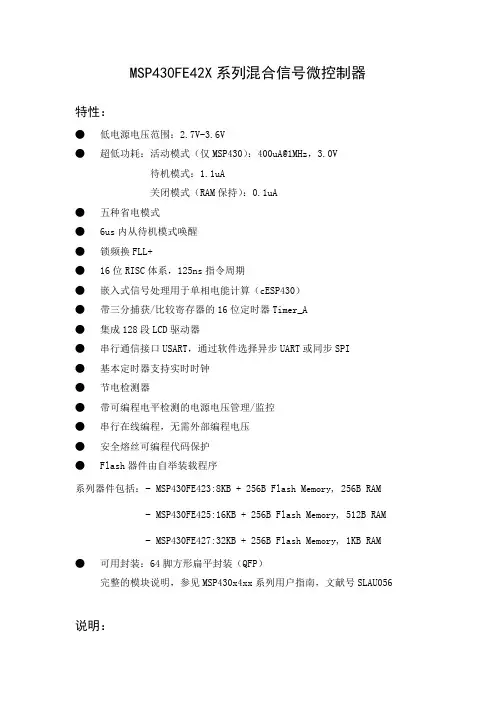
MSP430FE42X系列混合信号微控制器特性:●低电源电压范围:2.7V-3.6V●超低功耗:活动模式(仅MSP430):400uA@1MHz,3.0V待机模式:1.1uA关闭模式(RAM保持):0.1uA●五种省电模式●6us内从待机模式唤醒●锁频换FLL+●16位RISC体系,125ns指令周期●嵌入式信号处理用于单相电能计算(cESP430)●带三分捕获/比较寄存器的16位定时器Timer_A●集成128段LCD驱动器●串行通信接口USART,通过软件选择异步UART或同步SPI●基本定时器支持实时时钟●节电检测器●带可编程电平检测的电源电压管理/监控●串行在线编程,无需外部编程电压●安全熔丝可编程代码保护●Flash器件由自举装载程序系列器件包括:− MSP430FE423:8KB + 256B Flash Memory, 256B RAM− MSP430FE425:16KB + 256B Flash Memory, 512B RAM− MSP430FE427:32KB + 256B Flash Memory, 1KB RAM●可用封装:64脚方形扁平封装(QFP)完整的模块说明,参见MSP430x4xx系列用户指南,文献号SLAU056 说明:德州仪器MSP430系列超低功耗控制器由针对多种不同应用具有不同外围模块的芯片组成的。
器结构与五种低功耗模式相结合,适合在便携测量应用中实现延长电池寿命。
芯片具有强大的16位精简指令集,16位寄存器和常数发生器,可以实现最大代码执行效率。
带数字控制振荡器的锁频环FLL+提供从低功耗模式到活动模式小于6us的迅速唤醒。
MSP430FE42X系列是一块配置有三个独16位∑-△模式转换器的微控制器,内嵌入式信号处理器内核、特殊应用包括单项二线和单相三线电能表,可应用在防窃电电表功能中。
可用选项引脚说明:功能框图:引脚功能简要说明CPUMSP430 CPU具有一个16位精简指令结构,对应用来说是高透明的。

MSP430F552X中文手册及例程一、先写一篇开个头:这样快速闯入MSP430学习过程进入各个电子产品公司的网站,招聘里面嵌入式占据了大半工程师职位。
广义的嵌入式无非几种:传统的什么51单片机、 MSP430称做嵌入式微控制器;ARM是嵌入式微处理器;当然还有DSP;FPGA。
我们现在就不说别的,就说MSP430单片机,多数想学MSP430的童鞋,对89C51内核系列的单片机是很熟悉的,为了加深对MSP430 系列单片机的认识吗,迅速闯入MSP430学习过程,就必须彻底了解MSP430单片机,我们不妨将51单片机和MSP430两者进行一下比较。
第一点, 51内核单片机是8 位单片机。
其指令是采用的被称为“ CISC ”的复杂指令集,共具有111 条指令。
而MSP430 单片机是16 位的单片机,采用了精简指令集( RISC )结构,只有简洁的27 条指令,大量的指令则是模拟指令,众多的寄存器以及片内数据存储器都可参加多种运算。
这些内核指令均为单周期指令,功能强,运行的速度快。
第二点,MCU主要分为两种工作模式:待机与执行。
51内核单片机正常情况下消耗的电流为mA级 ,在掉电状态下,其耗电电流仍约为3mA左右 ;即使在掉电方式下,电源电压可以下降到2V ,但是为了保存内部RAM 中的数据,还需要提供约50uA的电流。
而430单片机功耗是在uA级的,工作电流极小,并且超低功耗,关断状态下的电流仅为0.1μA,待机电流为0.8μA,常规模式下的(250μA/1MIPS@3V),端口漏电流不足50 nA,并可零功耗掉电复位(BOR)。
另外,该芯片属低电器件,仅需1.8~3.6V电压供电,因而可有效降低系统功耗。
MSP430将低功耗模式扩展为7种,分别对应不同应用场合及任务的低功耗方式。
以睡眠模式为例,包括深度睡眠模式RTC:只有时钟在跑而其他都不动,目前,TI宣布其MSP430在RTC模式下最低功耗仅为360nA。
MSP430Microcontroller BasicsMSP430Microcontroller Basics John H.DaviesAMSTERDAM•BOSTON•HEIDELBERG•LONDONNEW YORK•OXFORD•PARIS•SAN DIEGOSAN FRANCISCO•SINGAPORE•SYDNEY•TOKYONewnes is an imprint of ElsevierNewnes is an imprint of Elsevier30Corporate Drive,Suite400,Burlington,MA01803,USALinacre House,Jordan Hill,Oxford OX28DP,UKCopyright©2008,Elsevier Ltd.All rights reserved.No part of this publication may be reproduced,stored in a retrieval system,or transmitted in any formor by any means,electronic,mechanical,photocopying,recording,or otherwise,without the prior written permission of the publisher.Permissions may be sought directly from Elsevier’s Science&Technology Rights Department in Oxford, UK:phone:(+44)1865843830,fax:(+44)1865853333,E-mail:************************.You may also complete your request online via the Elsevier homepage()by selecting “Support&Contact”then“Copyright and Permission”and then“Obtaining Permissions.”Recognizing the importance of preserving what has been written,Elsevier prints itsbooks on acid-free paper whenever possible.Library of Congress Cataloging-in-Publication DataApplication submittedBritish Library Cataloguing-in-Publication DataA catalogue record for this book is available from the British Library.ISBN:978-0-7506-8276-3For information on all Newnes publications,visit our Web site at:08091011121310987654321Printed in the United States of America“To Elizabeth.”ContentsPreface (xi)Chapter1:Embedded Electronic Systems and Microcontrollers (1)1.1What(and Where)Are Embedded Systems? (1)1.2Approaches to Embedded Systems (2)1.3Small Microcontrollers (5)1.4Anatomy of a Typical Small Microcontroller (8)1.5Memory (11)1.6Software (15)1.7Where Does the MSP430Fit? (16)Chapter2:The Texas Instruments MSP430 (21)2.1The Outside View—Pin-Out (21)2.2The Inside View—Functional Block Diagram (24)2.3Memory (25)2.4Central Processing Unit (30)2.5Memory-Mapped Input and Output (32)2.6Clock Generator (33)2.7Exceptions:Interrupts and Resets (36)2.8Where to Find Further Information (37)Chapter3:Development (43)3.1Development Environment (44)3.2The C Programming Language (46)3.3Assembly Language (55)3.4Access to the Microcontroller for Programming and Debugging (57)3.5Demonstration Boards (59)3.6Hardware (64)3.7Equipment (65)viii ContentsChapter4:A Simple Tour of the MSP430 (67)4.1First Program on a Conventional Desktop Computer (68)4.2Light LEDs in C (70)4.3Light LEDs in Assembly Language (72)4.4Read Input from a Switch (80)4.5Automatic Control:Flashing Light by Software Delay (91)4.6Automatic Control:Use of Subroutines (99)4.7Automatic Control:Flashing Light by Polling Timer_A (105)4.8Header Files and Issues Brushed under the Carpet (114)Chapter5:Architecture of the MSP430Processor (119)5.1Central Processing Unit (119)5.2Addressing Modes (125)5.3Constant Generator and Emulated Instructions (131)5.4Instruction Set (132)5.5Examples (146)5.6Reflections on the CPU and Instruction Set (153)5.7Resets (157)5.8Clock System (163)Chapter6:Functions,Interrupts,and Low-Power Modes (177)6.1Functions and Subroutines (178)6.2What Happens when a Subroutine Is Called? (178)6.3Storage for Local Variables (179)6.4Passing Parameters to a Subroutine and Returning a Result (183)6.5Mixing C and Assembly Language (185)6.6Interrupts (186)6.7What Happens when an Interrupt Is Requested? (188)6.8Interrupt Service Routines (190)6.9Issues Associated with Interrupts (196)6.10Low-Power Modes of Operation (198)Chapter7:Digital Input,Output,and Displays (207)7.1Digital Input and Output:Parallel Ports (208)7.2Digital Inputs (216)7.3Switch Debounce (225)7.4Digital Outputs (238)7.5Interface between3V and5V Systems (243)7.6Driving Heavier Loads (247)7.7Liquid Crystal Displays (252)7.8Driving an LCD from an MSP430x4xx (256)7.9Simple Applications of the LCD (264)Contents ix Chapter8:Timers (275)8.1Watchdog Timer (276)8.2Basic Timer1 (281)8.3Timer_A (287)8.4Measurement in the Capture Mode (300)8.5Output in the Continuous Mode (318)8.6Output in the Up Mode:Edge-Aligned Pulse-Width Modulation (330)8.7Output in the Up/Down Mode:Centered Pulse-Width Modulation (349)8.8Operation of Timer_A in the Sampling Mode (352)8.9Timer_B (353)8.10What Timer Where? (356)8.11Setting the Real-Time Clock:State Machines (357)Chapter9:Mixed-Signal Systems:Analog Input and Output (369)9.1Comparator_A (371)9.2Analog-to-Digital Conversion:General Issues (393)9.3Analog-to-Digital Conversion:Successive Approximation (402)9.4The ADC10Successive-Approximation ADC (407)9.5Basic Operation of the ADC10 (412)9.6More Advanced Operation of the ADC10 (424)9.7The ADC12Successive-Approximation ADC (432)9.8Analog-to-Digital Conversion:Sigma–Delta (438)9.9The SD16_A Sigma–Delta ADC (446)9.10Operation of SD16_A (459)9.11Signal Conditioning and Operational Amplifiers (475)9.12Digital-to-Analog Conversion (485)Chapter10:Communication (493)10.1Communication Peripherals in the MSP430 (495)10.2Serial Peripheral Interface (497)10.3SPI with the USI (504)10.4SPI with the USCI (513)10.5A Thermometer Using SPI in Mode3with the F2013as Master (520)10.6A Thermometer Using SPI in Mode0with the FG4618as Master (526)10.7Inter-integrated Circuit Bus (534)10.8A Simple I²C Master with the USCI_B0on a FG4618 (542)10.9A Simple I²C Slave with the USI on a F2013 (549)10.10State Machines for I²C Communication (559)10.11A Thermometer Using I²C with the F2013as Master (567)10.12Asynchronous Serial Communication (574)10.13Asynchronous Communication with the USCI_A (581)x Contents10.14A Software UART Using Timer_A (590)10.15Other Types of Communication (599)Chapter11:The Future:MSP430X (601)11.1Architecture of the MSP430X (601)11.2Instruction Set of the MSP430X (607)11.3Where Next? (614)11.4Conclusion (617)Appendix A:Kickstarting the MSP430 (619)A.1Introduction to EW430 (619)A.2Developing a Project in C (621)A.3Debugging with the Simulator (627)A.4Debugging with the Emulator (630)A.5Developing a Project in Assembly Language (633)A.6Tips for Using EW430 (636)A.7Tips for Specific Development Kits (640)Appendix B:Further Reading (645)Books and Articles (645)Newsletters,Magazines,and Journals (651)Index (655)Preface About a decade ago,I took over the teaching of afirst-year,second-semester course on digital electronics.It coveredflip-flops,counters,and state machines,all built fromsmall-scale integrated circuits.One of the projects at the end was to build a digital die.In many ways it was an excellent exercise because there were so many feasible ways in which it could be approached—simple counters,Johnson counters,or state machines.My concern was that it was very close to the project that I had experienced in myfirst course on digital electronics,which was back in the mid-1970s.The technology was close to the state of the art then,but was it still appropriate after so many years?Another feature of our course is that it is taken not only by electronic engineers but also by students from the science faculty,mostly computer scientists.I wanted these students to leave with a feeling for what can readily be done with modern programmable electronics insmaller-scale systems.I therefore replaced the material in the second half of the course with microcontrollers.(Do not worry,state machines were not abandoned—they are taught with hardware description languages in the context of programmable logic devices.) More recently,I thought that the time had come to review the choice of microcontroller. We traditionally used8-bit processors because modern devices have versatile peripherals and sophisticated embedded emulation and are quite powerful enough for most applications.Then the Texas Instruments MSP430caught my eye.A problem with8-bit microcontrollers is that8bits are too few for addresses,which are typically16bits long, and this means that data and addresses cannot be treated on an equal footing.In contrast, the MSP430has a uniform,16-bit architecture throughout:The address bus,data bus,and registers in the CPU are all16bits wide.The CPU has a modern design with plenty of registers,most of which can be used equally for data or addresses.It has a small instruction set with orthogonal addressing and an ingenious constant generator,which is used to emulate many operations that would otherwise need their own,distinct instructions.In many ways these features make the16-bit MSP430simpler than a typical8-bit processor.xii PrefaceOf course an elegant architecture does not generate many sales in the real world.More important are the range of peripherals and development tools.The MSP430offers the usual selection of peripherals plus some less common modules,including sigma–delta analog-to-digital converters and operational amplifiers.Some devices include hardware multipliers and digital-to-analog converters,which provide a complete signal chain(although,of course,Texas Instruments also offers an enormous range of digital signal processors).There is a choice of two free development environments(always an important considerationin education).One is IAR Embedded Workbench,which is available for a wide range of microcontrollers.Another,Code Composer Essentials,is produced by Texas Instruments itself.A third option is the GCC toolchain for MSP430at .I have not yet mentioned the major selling point of the MSP430,which is its low power consumption.Many microcontrollers are based on long-established designs withlow-power modes grafted onto them.This means that returning to full power from alow-power mode is often awkward and in some cases is virtually a reset operation.The MSP430is refreshingly different because it was designed from the outset for low-power operation.Entry to low-power modes and exit from them is straightforward,supported by a versatile clock system.For example,the clock module includes a digitally controlled oscillator that restarts at full speed from a low-power mode in less than1s in newer devices.In many applications the MSP430is put into a low-power mode,from which it is awakened by interrupts.These automatically restore full power for the interrupt service routine and return the processor to low power when it hasfinished.No extra code is needed for this:It is an intrinsic part of the interrupt mechanism.Most peripherals are designed for low power,although this can sometimes make them a little more complicated than would otherwise be necessary.The main point is that low-power modes are easy to use.The quality of the data sheets and user’s guides is another issue in education and those for the MSP430arefine.Unfortunately one item was missing in the area of documentation:a suitable textbook in English.I wrote this book tofill the gap.OutlineMost textbooks on microcontrollers follow one of two approaches.Thefirst is to present a sequence of projects to explore successive aspects of the device.I think that this works well for simpler architectures,notably the8-bit PICs,because it enables the reader to write functioning programs rapidly.This always feels good.Unfortunately I am not sure that it works as well for more advanced peripherals,which need considerable explanation before the reader can learn to use them fully.Preface xiii The alternative approach is to describe each module in the microcontroller fully and in turn,starting with the CPU and instruction set and working out to the peripherals.This makes for a well-organized reference book but can be tedious as a textbook.I tried to steer a course between these two.My inspiration is Kernighan and Ritchie’s The C Programming Language,which starts with a“Tutorial Introduction”before exploring the language systematically in subsequent chapters.I think that it takes rather more introduction to a microcontroller so the“simple tour,”which is my equivalent to the tutorial,does not start until Chapter4.Before that,thefirst chapter contains a general introduction to embedded systems and microcontrollers.This sets the scene for Chapter2, which focuses on the MSP430and gives a broad view of its features.I include a chapter on hardware and software for developing applications,which I hope will be particularly useful for readers who are new to microcontrollers.It also contains some reminders of features of the C language that are more prominent in programs for microcontrollers than desktop computers—bitfields for instance.This leads into the tour,which runs through some simple programs to illustrate input and output,the inevitableflashing LEDs,and an introduction to one of the timers(the MSP430has several).The remainder of the book provides a more systematic description of the MSP430.I start with the CPU and instruction set,and show how the constant generator is used to provide further“emulated”instructions.The clock system is also described in this chapter.It is followed by Chapter6on subroutines,interrupts,and low-power modes.I already mentioned that a major feature of the MSP430is the way in which low-power modes are handled automatically when interrupts are serviced.Subsequent chapters are concerned with the most widely used peripherals.Chapter7on digital input and output starts with the usual parallel ports and goes on to describe liquid crystal displays,which many MSP430s can drive directly.There is a wide selection of timers in the MSP430,which are covered in the next chapter.This is followed by a lengthy chapter on analog input and output.The MSP430offers many peripherals for analog-to-digital conversion,ranging from a simple comparator to a16-bit sigma–delta module.I do not think that you can use any of these without some understanding of their characteristics,which explains the length of this chapter.Some MSP430s include operational amplifiers and digital-to-analog converters,which I described briefly.Thefinal long chapter is on communication.I cover only three types of communication—serial peripheral interface,inter-integrated circuit bus,and asynchronous—but there are several peripherals for these in different variants of the MSP430,so there is a lot to explain.xiv PrefaceThe very last chapter provides an introduction to the MSP430X,an extended architecture with a20-bit address bus that can handle1MB of memory.There is also an appendix to take the reader through the steps of editing,building,and debugging thefirst project, which can sometimes be a frustrating experience.Ifind it annoying when books contain large chunks copied directly from data sheets and have tried to avoid this.You cannot hope to program a microcontroller without the data sheet at your side.Having said that,I start by going through each bit of the registers that control the peripherals used for the early programs.The idea is to explain how a typical peripheral is configured.After that I become more selective and concentrate on the overall function of the peripheral ually I pick out a few details that I think need extra explanation but skip the more mundane aspects.They are in the example programs inany case.I include links to many of Texas Instruments’application notes because I can see no point in repeating material that has been thoroughly explained already.Ifind that many students are strangely reluctant to use this valuable resource.There are a few reminders about code examples for the same reason.C or Assembly Language?Most small microcontrollers are now programmed using the C language so the question might seem redundant.In fact often columns in newletters on embedded systems often carry articles with titles such as“Is Assembly Language Dead?”However,the answer seems to be clearly that assembly language is not dead for small microcontrollers,such as the MSP430.Most code is written in C but you may occasionally need to write a subroutine in assembly language to perform an operation that cannot be written out directly in C.Two examples are operations that require bitwise rotations rather than shifts and calculations that can be done more efficiently by exploiting special instructions of the CPU,such as binary-coded decimal arithmetic.Intrinsic functions often avoid the need for assembly language but not always.More important,assembly language is often needed for debugging and this is the most compelling reason for describing it in a textbook.Small microcontrollers typically spend much of their time interacting with hardware by manipulating the registers that control the peripherals.Debugging may require stepping through lines of assembly language to check each step.You have to look at the manual to check the details of each instruction,but it helps to have a general idea of how the assembly language works.Preface xv From a pedagogical point of view,assembly language is useful to illustrate the architecture of the processor.In fact the MSP430is simple enough that you can explore the thinking behind the design of the instruction set.Besides,assembly language can be fun(in small doses).My approach is to develop thefirst,simple programs in Chapter4using both C and assembly language to show the relation between them.However,C dominates by the end of the chapter.Assembly language makes a strong showing in the next two chapters,which cover architecture,subroutines,and interrupts,including a section on mixing C and assembly language.Almost all remaining programs are in C,with assembly language reappearing only briefly for a function to convert numbers to binary-coded decimal.The listings in the text are read directly from the programs that I tested.Companion Web SitePlease visit the companion Web site for this book at/companions/9780750682763and download the programs used as examples in the book.These programs were read into the text of the book from the workspaces that I used for testing,which means that the downloadedfiles should match the book perfectly.Links are also provided for data sheets,user’s guides,and development tools.Solutions to the odd-numbered examples are freely available on the companion Web site but the remaining solutions are offered only to instructors. AcknowledgmentsIt is a pleasure to thank numerous people who have helped me in various ways to write this book.Many are from Texas Instruments:Bonnie Baker,Jacob Borgeson,Andreas Dannenberg,Colin Garlick,Thomas Mitnacht,and Robert Owen.I am particularly grateful to Adrian Valenzuela for his comments on thefinal draft.Several engineers from other companies were kind enough to provide advice and assistance:Edward Gibbins and Steve Duckworth from IAR,Tom Baugh of SoftBaugh,Paul Curtis of Rowley Associates,David Dyer of Ericsson and Fernando Rodriguez while he was at Texas Instruments.Finally,I am grateful to colleagues and students at Glasgow University,from whom I have learnt an enormous amount over the years.I’d like to thank Fernando Rodriguez(not the same person who was at Texas Instruments)and David Muir in particular,with both of whom I have run a wide range of projects on embedded systems and microcontrollers—from tutor boxes withflip-flops to the electronic systems of a Formula Student racing car.John Davies,Milngavie。

MSP430F2系列16位超低功耗单片机模块原理第10章通用串口界面Universal Serial Interface 版本: 1.5日期: 2007.5.原文: TI MSP430x2xxfamily.pdf翻译: 陈安都湖南长沙-中南大学编辑: DC 微控技术论坛版主注:以下文章是翻译TI MSP430x2xxfamily.pdf 文件中的部分内容。
由于我们翻译水平有限,有整理过程中难免有所不足或错误;所以以下内容只供参考.一切以原文为准。
详情请密切留意微控技术论坛。
Page 1 of 15通用串行接口模块(USI)提供与硬件模块的SPI和I2C串行通信。
本章讨论这两种模式。
USI模块包含在MSP420X20XX系列中。
主题10.1 USI的介绍10.2 USI的使用10.3 USI的寄存器10.1 USI的介绍USI模块提供支持同步串行通信的基本功能。
一般地,一个8、16位移位寄存器能用来输出数据流,少许的几条指令就可以执行串行通信。
另外,USI包含的内置硬件可以模拟SPI和I2C通信。
USI模块还包括中断,可以进一步减少串行通信的通用程序并且保持MSP430的低功耗特性。
USI模块的特性包括:支持三线SPI模式支持I2C模式可变的数据长度在LPM4方式下不需要内部时钟MSB或LSB指令可选在I2C模式下能控制SCL打开、停止监测在主机模式下的仲裁丢失监测可编程的时钟发生器可选择的钟极性和相位控制Page 2 of 15表10-1展示了SPI模式下的USI模块Page 3 of 15表10-2展示了I2C模式下的USI模块10.2 USI的操作USI模块主要由移位寄存器和位计数器组成,通过逻辑控制来支持SPI和I2C 通信。
USI的移位寄存器为USISR,通过软件直接控制数据的移入和移出。
位计数器计算采样位的数目以及在USICNTX位写零时设置USI中断标志位Page 4 of 15USIIFG。

/*MSP430F42X系列单片机16位ADC通用程序库说明:该驱动程序库包含了常用的16位ADC操作与控制功能函数,如选择通道、设置信号放大/*带有缓冲区及长短键的键盘通用程序库说明:该程序库包含了读取键盘的相关函数,并且包含了一个键盘缓冲区,当主程序执行较慢,而遇到连续快速的键盘输入来不及及时读取的情况下,新的按键信息将会自动存入键盘缓冲队列内,每次调用读键盘函数时会依顺序读取,保证键盘操作不会丢失。
并且带有长短按键识别功能,当按键时间小于2秒时,返回短键,按键超过2秒后,每隔0.25秒返回一次长按键。
该键盘程序可以作为各种程序的底层驱动使用。
要使用该库函数,需要将本文件(Key.c)添加进工程,并在需要调用键盘函数的文件开头处包含"Key.h";还需要开启一个定时器,在定时中断内调用Key_ScanIO()函数。
设置定时中断的频率在16~128次/秒之间。
*///+-------------+//|定时中断|软件结构//+-------------+//|//+-------------++-------------++-------------+// KEY1_IN -->| Key_ScanIO||KeyBuff[]||Key_GetKey() |// KEY2_IN -->|键盘扫描|-->|键盘缓冲|-->|Key_WaitKey()|-->应用程序// KEY3_IN -->|函数||队列(FIFO) ||键盘读取函数|//+-------------++-------------++-------------+//////MSP430F4XX//+---------------+//+---KEY1--|P1.5|//||XOUT|-----//+---KEY2--|P1.6|32.768KHz Watch Crystal//||XIN|-----//+---KEY3--|P1.7|//|+---------------+//GND//#include<msp430x42x0.h>#define KEYBUFF_SIZE8/*键盘缓冲区大小,根据程序需要自行调整*/ char KeyBuff[KEYBUFF_SIZE]; //定义键盘缓冲队列数组(FIFO)char Key_IndexW=0;//键盘缓冲队列写入指针(头指针)char Key_IndexR=0;//键盘缓冲队列读取指针(尾指针char Key_Count=0;//键盘缓冲队列内记录的按键次数char KEY1_State=0;char KEY2_State=0;char KEY3_State=0;/*3个按键的状态变量*/#define NOKEY0#define PUSH_KEY1#define LONG_PUSH 2#define KEY1_IN (P5IN&BIT5) //KEY1输入IO的定义(P6.4)#define KEY2_IN (P5IN&BIT6) //KEY2输入IO的定义(P6.5)#define KEY3_IN (P5IN&BIT7) //KEY3输入IO的定义(P6.6)#define KEY1 0x01//SET按键#define KEY2 0x02//增加按键#define KEY3 0x04//减小按键#define LONG0x80/*连续长键标志位宏定义*/#define FIRSTLONG 0xC0/*首次长键标志位宏定义*//***************************************************************** ************名称:Key_InBuff()*功能:将一次键值压入键盘缓冲队列*入口参数:Key:被压入缓冲队列的键值*出口参数:无********************************************************************* *******/void Key_InBuff(char Key){if(Key_Count>=KEYBUFF_SIZE) return;//若缓冲区已满,放弃本次按键_DINT();Key_Count++;//按键次数计数增加KeyBuff[Key_IndexW] = Key;//从队列头部追加新的数据if (++Key_IndexW >=KEYBUFF_SIZE) //循环队列,如果队列头指针越界{Key_IndexW = 0;//队列头指针回到数组起始位置}_EINT();}/*********************************************************** ******************名称:Key_GetKey()*功能:从键盘缓冲队列内读取一次键值*入口参数:无*出口参数:若无按键,返回0,否则返回一次按键键值。
Page 1 of 18MSP430F2系列16位超低功耗单片机模块原理第5章 Flash 块控制器版本: 1.3日期: 2007.6.原文: TI MSP430x2xxfamily.pdf翻译: 余川编辑: DC 微控技术论坛版主注:以下文章是翻译TI MSP430x2xxfamily.pdf 文件中的部分内容。
由于我们翻译水平有限,有整理过程中难免有所不足或错误;所以以下内容只供参考.一切以原文为准。
详情请密切留意微控技术论坛。
第五章 Flash 存储控制器本章介绍了MSP430x2xx 系列单片机Flash 存储控制器的操作。
5.1 Flash 存储器的介绍Page 2 of 18 5.2 Flash 存储器的分段结构5.3 Flash 存储器的操作5.4 Flash 存储器的控制寄存器5.1 Flash 存储器的介绍MSP430 的F lash 存储器是可位/字节/字寻址和编程的存储器。
该模块由一个集成控制器来控制编程和擦除的操作。
控制器包括三个寄存器,一个时序发生器及一个提供编程/擦除电压的电压发生器。
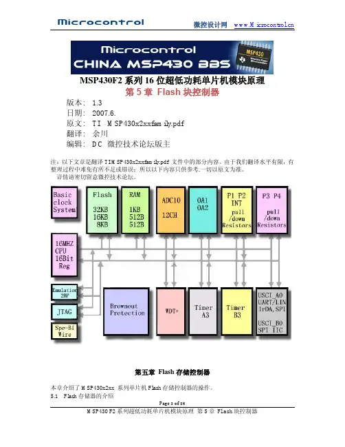
MSP430 的F lash 存储器的特点有:● 产生内部编程电压● 可位/字节/字编程● 超低功耗操作● 支持段擦除和多段模块擦除F lash 存储器和控制器的结构框图如图5−1所示。
注意:F lash 写入和擦除操作期间的最小电压值V CC 应为2.2V 。
如果在操作期间V CC 低于2.2V ,写入或擦除的结果将是不确定的。
图5−1 F lash 存储器框图Page 3 of 185.2 Flash 存储器的分段结构MSP430 F lash 存储器分成多个段。
可对其进行单个位/字节/字的写入,但是最小的擦除单位是段。
F lash 存储器分为主存储器和信息存储器两部分,在操作上两者没有什么区别,程序代码和数据可以存储于任意部分。
两部分的区别在于段的大小和物理地址。
信息存储器有四个64字节的段,主存储器有两个或更多的512字节的段。
IAR Embedded Workbench™Version3+ for MSP430™User's GuideLiterature Number:SLAU138AFJune2004–Revised June2014Contents Preface (6)1Get Started Now! (8)1.1Software Installation (9)1.2Flashing the LED (9)1.3Important MSP430Documents on the CD-ROM and Web (10)2Development Flow (11)2.1Overview (12)2.2Using KickStart (12)2.2.1Project Settings (13)2.2.2Using Math Library for MSP430(MSPMathlib)in IAR EW4305.60.1and Newer (14)2.2.3Additional Project Settings for MSP430L092and MSP430C092 (14)2.2.4Creating a Project From Scratch (16)2.2.5Additional Project Settings for Ultra-Low-Power Mode(LPMx.5)Debugging (17)2.2.6Password Protection for MSP430Devices (18)2.2.7Using an Existing IAR V1.x,V2.x,or V3.x Project (18)2.2.8Stack Management and.xcl Files (19)2.2.9How to Generate Texas Instruments.TXT(and Other Format)Files (19)2.2.10Overview of Example Programs (19)2.3Using C-SPY (19)2.3.1Breakpoint Types (19)2.3.2Using Breakpoints (22)2.3.3Using Single Step (22)2.3.4Using Watch Windows (23)3EnergyTrace™Technology (24)3.1Introduction (24)3.2Energy Measurement (24)3.3IAR Embedded Workbench®for MSP430Integration (24)3.3.1Debugging Devices With EnergyTrace++Technology Support (24)3.3.2Debugging Devices Without EnergyTrace++Technology Support (31)3.4Measuring Low-Power Currents (34)3.5EnergyTrace Technology FAQs (35)4Memory Protection Unit(MPU)and Intellectual Property Encapsulation(IPE) (37)A Frequently Asked Questions (38)A.1Hardware (39)A.2Program Development(Assembler,C-Compiler,Linker) (39)A.3Debugging(C-SPY) (41)B FET-Specific Menus (45)B.1Menus (46)B.1.1Emulator→Device Information (46)B.1.2Emulator→Release JTAG on Go (46)B.1.3Emulator→Resynchronize JTAG (46)B.1.4Emulator→Init New Device (46)B.1.5Emulator→Secure-Blow JTAG Fuse (46)B.1.6Emulator→Breakpoint Usage (46)2Contents SLAU138AF–June2004–Revised June2014Submit Documentation FeedbackCopyright©2004–2014,Texas Instruments IncorporatedB.1.7Emulator→Advanced→Clock Control (46)B.1.8Emulator→Advanced→Emulation Mode (46)B.1.9Emulator→Advanced→Memory Dump (47)B.1.10Emulator→Advanced→Breakpoint Combiner (47)B.1.11Emulator→State Storage Control (47)B.1.12Emulator→State Storage Window (47)B.1.13Emulator→Sequencer Control (47)B.1.14Emulator→"Power on"Reset (47)B.1.15Emulator→GIE on/off (47)B.1.16Emulator→Leave Target Running (47)B.1.17Emulator→Force Single Stepping (47)Revision History (48)3 SLAU138AF–June2004–Revised June2014Contents Submit Documentation FeedbackCopyright©2004–2014,Texas Instruments IncorporatedList of Figures1-1.Activate Project (9)1-2.Activate Project in Workspace Overview (10)2-1.L092Mode (14)2-2.C092Emulation Mode (15)2-3.C092Password (15)2-4.Enable Ultra-Low-Power Debug Mode (17)2-5.LPMx.5Notifications (18)2-6.JTAG Password (18)3-1.Pulse Density and Current Flow (24)3-2.Debug Session With EnergyTrace++Windows (25)3-3.Debug Options (26)3-4.Emulator Pulldown Menu With EnergyTrace++-Related Functions (27)3-5.Enabling the State Log Window (27)3-6.State Log Window With EnergyTrace++Data (28)3-7.State Log Summary With EnergyTrace++Data (28)3-8.Power Log Setup Window (28)3-9.Power Log Window With EnergyTrace++Data (29)3-10.Timeline With Power Log and State Graphs Disabled (29)3-11.Timeline With EnergyTrace++Data (30)3-12.Function Profiler With EnergyTrace++Data (30)3-13.Debug Session With EnergyTrace Windows (31)3-14.Emulator Pulldown Menu With EnergyTrace-Related Functions (32)3-15.Power Log Setup Window (32)3-16.Power Log Window With EnergyTrace Data (33)3-17.Timeline With Power Log Graph Disabled (33)3-18.Timeline With EnergyTrace Data (34)3-19.LPM3Current When Executing Under Debug Control (34)3-20.Release JTAG on Go Option in Emulator Pulldown Menu (35)3-21.LPM3Current When Executing with JTAG Signals Released (35)4-1.MPU Configuration Dialog (37)4List of Figures SLAU138AF–June2004–Revised June2014Submit Documentation FeedbackCopyright©2004–2014,Texas Instruments IncorporatedList of Tables2-1.Device Architecture,Breakpoints,and Other Emulation Features (20)5 SLAU138AF–June2004–Revised June2014List of Tables Submit Documentation FeedbackCopyright©2004–2014,Texas Instruments IncorporatedPrefaceSLAU138AF–June2004–Revised June2014Read This FirstAbout This ManualThis manual describes the use of IAR Embedded Workbench®(EW430)with the MSP430™ultra-low-power microcontrollers.How to Use This ManualRead and follow the instructions in the Get Started Now!chapter.This chapter provides instructions on installing the software,and describes how to run the demonstration programs.After you see how quick and easy it is to use the development tools,TI recommends that you read all of this manual.This manual describes only the setup and basic operation of the software development environment,but it does not fully describe the MSP430microcontrollers or the complete development software and hardware systems.For details of these items,see the appropriate TI and IAR™documents listed in RelatedDocumentation From Texas Instruments,Important MSP430Documents on the CD-ROM and Web.This manual applies to the use with Texas Instruments'MSP-FET430UIF,MSP-FET430PIF,and eZ430 development tools series.These tools contain the most up-to-date materials available at the time of packaging.For the latestmaterials(including data sheets,user's guides,software,and application information),visit the TI MSP430 web site at /msp430or contact your local TI sales office.Information About Cautions and WarningsThis book may contain cautions and warnings.CAUTIONThis is an example of a caution statement.A caution statement describes a situation that could potentially damage yoursoftware or equipment.The information in a caution or a warning is provided for your protection.Read each caution and warning carefully.MSP430,EnergyTrace are trademarks of Texas Instruments.6Read This First SLAU138AF–June2004–Revised June2014 IAR Embedded Workbench is a registered trademark of IAR Systems AB.Submit Documentation Feedback All other trademarks are the property of their respective owners.Copyright©2004–2014,Texas Instruments Incorporated Related Documentation From Texas Instruments Related Documentation From Texas InstrumentsMSP430development tools documentationMSP430Hardware Tools User's Guide,literature number SLAU278eZ430-F2013Development Tool User's Guide,literature number SLAU176eZ430-RF2480User's Guide,literature number SWRA176eZ430-RF2500Development Tool User's Guide,literature number SLAU227eZ430-RF2500-SEH Development Tool User's Guide,literature number SLAU273eZ430-Chronos Development Tool User's Guide,literature number SLAU292MSP430device data sheetsMSP430x1xx Family User's Guide,literature number SLAU049MSP430x2xx Family User's Guide,literature number SLAU144MSP430x3xx Family User's Guide,literature number SLAU012MSP430x4xx Family User's Guide,literature number SLAU056MSP430x5xx and MSP430x6xx Family User's Guide,literature number SLAU208MSP430FR57xx Family User's Guide,literature number SLAU272MSP430FR58xx,MSP430FR59xx,MSP430FR68xx,and MSP430FR69xx Family User's Guide,literature number SLAU367CC430device data sheetsCC430Family User's Guide,literature number SLAU259If You Need AssistanceSupport for the MSP430devices and the FET development tools is provided by the Texas Instruments Product Information Center(PIC).Contact information for the PIC can be found on the TI web site at/support.The Texas Instruments E2E Community support forums for the MSP430is available to provide open interaction with peer engineers,TI engineers,and other experts.Additional device-specific information can be found on the MSP430web site.NOTE:The KickStart kit is supported by Texas Instruments.Although the KickStart kit is a product of IAR,Texas Instruments provides the support for it.Therefore,please do not request support for KickStart from IAR.Consult the extensivedocumentation provided with KickStart before requesting assistance.7 SLAU138AF–June2004–Revised June2014Read This First Submit Documentation FeedbackCopyright©2004–2014,Texas Instruments IncorporatedChapter1SLAU138AF–June2004–Revised June2014Get Started Now!This chapter provides instruction on installing the software,and shows how to run the demonstration programs.Topic Page1.1Software Installation (9)1.2Flashing the LED (9)1.3Important MSP430Documents on the CD-ROM and Web (10)8Get Started Now!SLAU138AF–June2004–Revised June2014Submit Documentation FeedbackCopyright©2004–2014,Texas Instruments Incorporated Software Installation 1.1Software InstallationFollow the instructions on the supplied READ ME FIRST document to install the IAR EmbeddedWorkbench™KickStart kit.Read the file<Installation Root>\Embedded Workbenchx.x\430\doc\readme.htm from IAR for the latest information about the Workbench.The term KickStartrefers to the function-limited version of Embedded Workbench(including C-SPY™debugger).KickStart is supplied on the CD-ROM included with each FET,and the latest version is available from the MSP430 web site.The documents mentioned in the previous paragraph(and this document)can be accessed using:Start→Programs→IAR Systems→IAR Embedded Workbench KickStart for MSP430V3.KickStart is compatible with Windows2000(SP4),Windows XP(32bit and64bit),Windows Vista(32bit and64bit),and Windows7(32bit and64bit).However,the USB FET interface works with only Windows XP(32bit and64bit),Windows Vista(32bit and64bit),and Windows7(32bit and64bit).1.2Flashing the LEDThis section demonstrates on the FET the equivalent of the C-language"Hello World!"introductoryprogram.An application that flashes the LED is developed and downloaded to the FET,and then run.1.Start the Workbench(Start→Programs→IAR Systems→IAR Embedded Workbench KickStart forMSP430V3→IAR Embedded Workbench).2.Click File→Open Workspace to open the file at:<Installation Root>\Embedded Workbench x.x\430\FET_examples\Flashing the LED.eww.The workspace window opens.3.Click on the tab at the bottom of the workspace window that corresponds to the MSP430device(MSP430xxxx)and desired language(assembler or C)to set a project active(see Figure1-1).Figure1-1.Activate Project9 SLAU138AF–June2004–Revised June2014Get Started Now! Submit Documentation FeedbackCopyright©2004–2014,Texas Instruments IncorporatedImportant MSP430Documents on the CD-ROM and Web Alternatively,right click to activate a project in the Workspace Overview tab(see Figure1-2).Figure1-2.Activate Project in Workspace Overview4.Click Project→Options→FET Debugger→Setup→Connection to select the appropriate port:Texas Instruments LPT-IF for the parallel FET Interface(MSP-FET430PIF)or Texas Instruments USB-IF for the USB Interface(MSP-FET430UIF)or for the eZ430.5.Click Project→Rebuild All to build and link the source code.You can view the source code by double-clicking on the project,and then double-clicking on the displayed source file.6.Click Project→Debug to start the C-SPY debugger.C-SPY erases the device flash and thendownloads the application object file to the device flash.See FAQ Debugging#1if C-SPY is unable to communicate with the device.7.Click Debug→Go to start the application.The LED should flash.8.Click Debug→Stop Debugging to stop debugging,to exit C-SPY,and to return to the Workbench.9.Click File→Exit to exit the Workbench.Congratulations,you have just built and tested an MSP430application!1.3Important MSP430Documents on the CD-ROM and WebThe primary sources of MSP430information are the device-specific data sheet and user's guide.The most up-to-date versions of these documents that are available at the time of production are provided on the CD-ROM included with this tool.The MSP430web site(/msp430)contains the most recent version of these documents.PDF documents describing the IAR tools(Workbench and C-SPY,the assembler,the C compiler,thelinker,and the librarian)are in the common\doc and430\doc folders.Supplements to the documents(that is,the latest information)are available in HTML format in the same directories.430\doc\readme_start.htm provides a convenient starting point for navigating the IAR documentation.10Get Started Now!SLAU138AF–June2004–Revised June2014Submit Documentation FeedbackCopyright©2004–2014,Texas Instruments IncorporatedChapter2SLAU138AF–June2004–Revised June2014Development Flow This chapter describes how to use KickStart to develop application software and how to use C-SPY to debug it.Topic Page2.1Overview (12)2.2Using KickStart (12)2.3Using C-SPY (19)11 SLAU138AF–June2004–Revised June2014Development Flow Submit Documentation FeedbackCopyright©2004–2014,Texas Instruments IncorporatedOverview 2.1OverviewApplications are developed in assembler or C using the Workbench,and they are debugged using C-SPY.C-SPY is seamlessly integrated into the Workbench.However,it is more convenient to make thedistinction between the code development environment(Workbench)and the debugger(C-SPY).C-SPY can be configured to operate with the FET(that is,an actual MSP430device)or with a software simulator of the device.KickStart refers to the Workbench and C-SPY collectively.The KickStart software tools area product of IAR.Documentation for the MSP430family and KickStart is extensive.The CD-ROM supplied with this toolcontains a large amount of documentation describing the MSP430.The MSP430home page(/msp430)is another source of MSP430information.The components of KickStart(workbench and debugger,assembler,compiler,linker)are fully documented in<Installation Root>\EmbeddedWorkbench x.x\common\doc and<Installation Root>\Embedded Workbench\430\doc..htm files located throughout the KickStart directory tree contain the most up-to-date information and supplement the PDF files.In addition,KickStart documentation is available online via Help.Read Me First files from IAR and TI and this document can be accessed using Start→Programs→IAR Systems→IAR Embedded Workbench KickStart for MSP430V3.Tool User's Guide Most Up-To-Date Information Workbench,C-SPY EW430_UsersGuide.pdf readme.htm,ew430.htm,cs430.htm,cs430f.htmAssembler EW430_AssemblerReference.pdf a430.htm,a430_msg.htmCompiler EW430_CompilerReference.pdf icc430.htm,icc430_msg.htmC library CLibrary.htmLinker and Librarian xlink.pdf xlink.htm,xman.htm,xar.htm2.2Using KickStartThe KickStart edition is a special starter kit or evaluation version of IAR Embedded Workbench withlimitations both in code size and in the service and support that is provided.Limitations:•The C compiler does not generate an assembly code list file.•The code size limit of the MSP430IAR KickStart C/C++Compiler is set to4Kbytes for traditional MSP430devices and8Kbytes for MSP430X devices(see Table2-1for detailed information aboutwhich MSP430device is based on which architecture).•The IAR Assembler delivered is the full version without any restrictions.•The IAR XLINK Linker links a maximum of4Kbytes originating from C source code for traditional MSP430devices and8Kbytes for MSP430X devices(see Table2-1for detailed information aboutwhich MSP430device is based on which architecture),but an unlimited amount of code originatingfrom assembly code.•The IAR KickStart C-SPY Simulator reads a maximum of4Kbytes originating from C code for traditional MSP430devices and8Kbytes for MSP430X devices but is unlimited in the amount ofassembly code read(see Table2-1for detailed information about which MSP430device is based onwhich architecture).•MISRA C is not available.•The runtime library source code is not included.A full(that is,unrestricted)version of the software tools can be purchased from IAR.A mid-featured toolset–called Baseline,with a12Kbyte C-code size limitation and basic floating-point operations–is also available from IAR.See the IAR web site(www.iar.se)for more information.12Development Flow SLAU138AF–June2004–Revised June2014Submit Documentation FeedbackCopyright©2004–2014,Texas Instruments Incorporated Using KickStart 2.2.1Project SettingsThe settings required to configure the Workbench and C-SPY are numerous and detailed.Read andthoroughly understand the documentation supplied by IAR when dealing with project settings.Review the project settings of the supplied assembler and C examples(the project settings are accessed usingProject→Options with the project name selected).Use these project settings as templates whendeveloping your own projects.Note that if the project name is not selected when settings are made,the settings are applied to the selected file(not to the project).The following project settings are recommended or required:•Specify the target device(General Options→Target→Device).•Enable an assembler project or a C or assembler project(General Options→Target→Assembler-only project).•Enable the generation of an executable output file(General Options→Output→Output file→Executable).•To most easily debug a C project,disable optimization[C/C++Compiler→Optimizations→Size→None(Best debug support)].•Enable the generation of debug information in the compiler output(C/C++Compiler→Output→Generate debug information).•Specify the search path for the C preprocessor(C/C++Compiler→Preprocessor→Include Paths).•Enable the generation of debug information in the assembler output(Assembler→Output→Generate Debug Info).•Specify the search path for the assembler preprocessor(Assembler→Preprocessor→Include Paths).•To debug the project using C-SPY,specify a compatible format[Linker→Output→Format→Debug information for C-SPY(with runtime control modules or with I/O emulation modules)].•Specify the search path for any used libraries(Linker→Config→Search paths).•Specify the C-SPY driver.Select Project→Options→Debugger→Setup→Driver→FET Debugger to debug on the FET(that is,MSP430device).Select Simulator to debug on the simulator.If FETDebugger is selected,use Project→Options→FET Debugger→Setup→Connection to select theappropriate port:Texas Instruments LPT-IF for the parallel FET Interface(MSP-FET430PIF)or TexasInstruments USB-IF for the USB Interface(MSP-FET430UIF)or for the eZ430.•Enable the Device Description file.This file makes C-SPY"aware"of the specifics of the device it is debugging.This file corresponds to the specified target device(Debugger→Setup→Devicedescription file→Override default).•Enable the erasure of the Main and Information memories before object code download(FET Debugger→Download→Erase main and Information memory).•To maximize system performance during debug,disable Virtual Breakpoints(FET Debugger→Breakpoints→Use virtual breakpoints)and disable all System Breakpoints(FET Debugger→Breakpoints→System breakpoints on).NOTE:Use Factory Settings to quickly configure a project.Use the Factory Settings button to quickly configure a project to a usable state.The following steps can be used to quickly configure a project.Note that the General Options tab does not have a Factory Settings button.1.Specify the target device(General Options→Target→Device).2.Enable an assembler project or a C or assembler project(General Options→Target→Assembler-only project).3.Enable the generation of an executable output file(General Options→Output→Output file→Executable).4.Accept the factory settings for the compiler(C/C++Compiler→Factory Settings).5.Accept the factory settings for the assembler(Assembler→Factory Settings).13 SLAU138AF–June2004–Revised June2014Development Flow Submit Documentation FeedbackCopyright©2004–2014,Texas Instruments IncorporatedUsing KickStart 6.Accept the factory settings for the linker(Linker→Factory Settings).7.Accept the factory settings for C-SPY(Debugger→Factory Settings).8.Debug on the hardware(Debugger→Setup→Driver→FET Debugger).9.Specify the active parallel port used to interface to the FET if not LPT1(FET Debugger→Setup→Connection→Texas Instruments LPT-IF)or specify the USB port(FET Debugger→Setup→Connection→Texas Instruments USB-IF).NOTE:Avoid the use of absolute path names when referencing files.Instead,use the relative pathname keywords$TOOLKIT_DIR$and$PROJ_DIR$.See theIAR documentation for a description of these keywords.The use of relative path namespermits projects to be moved easily,and projects do not require modification when IARsystems are upgraded(for example,from KickStart or Baseline to Full).2.2.2Using Math Library for MSP430(MSPMathlib)in IAR EW4305.60.1and NewerTI's MSPMathlib is part of EW4305.60.1and newer releases.This optimized library provides up to26x better performance in applications that use floating point scalar math.For details,see the MSPMathlibweb page(/tool/mspmathlib).MSPMathlib may be enabled for new and existing projects on all supported devices.Enable or disable MSPMathlib in the project options(General Options→Library Configuration→MathLib).2.2.3Additional Project Settings for MSP430L092and MSP430C092The MSP430L092can operate in two different modes:L092mode and C092emulation mode.Thepurpose of the C092emulation mode is to behave like a C092with up to1920bytes of code at its final destination for mask generation.The operation mode is determined by EW430before starting the debugger.Two radio buttons areavailable for the mode selection.By default the L092mode is selected(see Figure2-1and Figure2-2).Figure2-1.L092Mode14Development Flow SLAU138AF–June2004–Revised June2014Submit Documentation FeedbackCopyright©2004–2014,Texas Instruments Incorporated Using KickStartFigure2-2.C092Emulation Mode2.2.3.1MSP430L092Loader CodeThe Loader Code in the MSP430L092is a ROM-code from TI that provides a series of services.It enables customers to build autonomous applications without needing to develop a ROM mask.Such an application consists of an MSP430device containing the loader(for example,MSP430L092)and an SPI memorydevice(for example,'95512or'25AA40);these and similar devices are available from variousmanufacturers.The majority of use cases for an application with a loader device and external SPI memory for native0.9-V supply voltage are late development,prototyping,and small series production.Figure2-1shows the selection for loading the application into the external SPI memory.2.2.3.2Password Protection of MSP430C092The MSP430C092is a customer-specific ROM device that is protected by a password.To start a debug session,the password must be provided to EW430.Figure2-3shows how to provide a HEX password in EW430.Figure2-3.C092Password15 SLAU138AF–June2004–Revised June2014Development Flow Submit Documentation FeedbackCopyright©2004–2014,Texas Instruments IncorporatedUsing KickStart 2.2.4Creating a Project From ScratchThis section presents step-by-step instructions to create an assembler or C project from scratch,and to download and run the application on the MSP430(see also Section2.2.1,Project Settings).The MSP430 IAR Embedded Workbench IDE User's Guide presents a more comprehensive overview of the process.1.Start the Workbench(Start→Programs→IAR Systems→IAR Embedded Workbench KickStart forMSP430V3→IAR Embedded Workbench).2.Create a new text file(File→New→File).3.Enter the program text into the file.NOTE:Use.h files to simplify your code development.KickStart is supplied with files that define the device registers and the bit names for eachdevice.These files can greatly simplify the task of developing your program.The files arelocated in<Installation Root>\Embedded Workbench x.x\430\inc.Include the.h filecorresponding to your target device in your text file(#include"msp430xyyy.h").Additionally,files io430xxxx.h are provided and are optimized to be included by C source files.4.Save the program text file(File→Save).It is recommended that assembler text files be saved with a file-type suffix of".s43"and that C text files be saved with a file-type suffix of".c".5.Create a new workspace(File→New→Workspace).6.Create a new project(Project→Create New Project).Select Tool chain:MSP430,Project Templates:Empty project and click OK.Specify a project name and click Save.7.Add the program text file to the project(Project→Add Files).Select the program text file and clickOpen.Alternatively,double-click on the file to add it to the project.NOTE:How to add assembler source files to your projectThe default file type presented in the Add Files window is"C/C++Files".To view assemblerfiles(.s43),select"Assembler Files"in the"Files of type"drop-down menu.8.Save the workspace(File→Save Workspace).Specify a workspace name and click Save.9.Configure the project options(Project→Options).For each of the subcategories(General Options,C/C++Compiler,Assembler,Linker,Debugger),accept the default Factory Settings with the followingexceptions:•Specify the target device(General Options→Target→Device).•Enable an assembler project or a C or assembler project(General Options→Target→Assembler-only project).•Enable the generation of an executable output file(General Options→Output→Output file→Executable).•To debug on the FET(that is,the MSP430),click Debugger→Setup→Driver→FET Debugger.•Specify the active port used to interface to the FET(FET Debugger→Setup→Connection).10.Build the project(Project→Rebuild All).11.Debug the application using C-SPY(Project→Debug).This starts C-SPY,and C-SPY takes control ofthe target,erases the target memory,programs the target memory with the application,and resets thetarget.See FAQ Debugging#1if C-SPY is unable to communicate with the device.12.Click Debug→Go to start the application.13.Click Debug→Stop Debugging to stop the application,to exit C-SPY,and to return to the Workbench.14.Click File→Exit to exit the Workbench.16Development Flow SLAU138AF–June2004–Revised June2014Submit Documentation FeedbackCopyright©2004–2014,Texas Instruments Incorporated Using KickStart 2.2.5Additional Project Settings for Ultra-Low-Power Mode(LPMx.5)Debugging2.2.5.1What is LPMx.5LPMx.5is an ultra-low-power mode in which the entry and exit is handled differently than the other low-power modes.LPMx.5gives the lowest power consumption available on a device.To achieve this,entry to LPMx.5disables the LDO of the PMM module,which removes the supply voltage from the core and the JTAGmodule of the device.Because the supply voltage is removed from the core,all register contents andSRAM contents are lost.Exit from LPMx.5causes a BOR event,which forces a complete reset of thesystem.NOTE:The option"RELEASE JTAG ON GO"is currently not supported in the EmbeddedWorkbench when LPMx.5debugging is active.See the MSP430device family user's guidefor additional LPMx.5and ultra-low-power debug mode details.2.2.5.2Enable Ultra-Low-Power Debug ModeTo enable the ultra-low power debug mode feature the“Enable ULP/LPMx.5debug”checkbox must be enabled by clicking FET Debugger->Setup->Enable ULP/LPMx.5debug(see Figure2-4).When the ultra-low power debug mode is enabled a notification is displayed in the Debugger log every time thetarget device enters and leaves LPMx.5mode(see Figure2-5).Press the Halt or Reset button in Embedded Workbench to wake up the target device from LPMx.5.Execution of the code is halted at the start of the program.All breakpoints that had been active beforeLPMx.5are restored and reactivated automatically.Figure2-4.Enable Ultra-Low-Power Debug Mode17 SLAU138AF–June2004–Revised June2014Development Flow Submit Documentation FeedbackCopyright©2004–2014,Texas Instruments Incorporated。
IMPORTANT NOTICETexas Instruments Incorporated and its subsidiaries (TI) reserve the right to make corrections, modifications, enhancements, improvements, and other changes to its products and services at any time and to discontinue any product or service without notice. Customers should obtain the latest relevant information before placing orders and should verify that such information is current and complete. All products are sold subject to TI’s terms and conditions of sale supplied at the time of order acknowledgment.TI warrants performance of its hardware products to the specifications applicable at the time of sale in accordance with TI’s standard warranty. T esting and other quality control techniques are used to the extent TI deems necessary to support this warranty. Except where mandated by government requirements, testing of all parameters of each product is not necessarily performed.TI assumes no liability for applications assistance or customer product design. Customers are responsible for their products and applications using TI components. T o minimize the risks associated with customer products and applications, customers should provide adequate design and operating safeguards.TI does not warrant or represent that any license, either express or implied, is granted under any TI patent right, copyright, mask work right, or other TI intellectual property right relating to any combination, machine, or process in which TI products or services are used. Information published by TI regarding third-party products or services does not constitute a license from TI to use such products or services or a warranty or endorsement thereof. Use of such information may require a license from a third party under the patents or other intellectual property of the third party, or a license from TI under the patents or other intellectual property of TI.Reproduction of information in TI data books or data sheets is permissible only if reproduction is without alteration and is accompanied by all associated warranties, conditions, limitations, and notices. Reproduction of this information with alteration is an unfair and deceptive business practice. TI is not responsible or liable for such altered documentation.Resale of TI products or services with statements different from or beyond the parameters stated by TI for that product or service voids all express and any implied warranties for the associated TI product or service and is an unfair and deceptive business practice. TI is not responsible or liable for any such statements. Following are URLs where you can obtain information on other Texas Instruments products and application solutions:Products ApplicationsAmplifiers Audio /audioData Converters Automotive /automotiveDSP Broadband /broadbandInterface Digital Control /digitalcontrolLogic Military /militaryPower Mgmt Optical Networking /opticalnetwork Microcontrollers Security /securityTelephony /telephonyVideo & Imaging /videoWireless /wirelessMailing Address:Texas InstrumentsPost Office Box 655303 Dallas, Texas 75265Copyright 2004, Texas Instruments Incorporated。
MSP432 产品培训目录第一章MSP432™ MCU概览 (2)第二章 Cortex-M4F内核和中断 (14)第三章电源系统 (20)未完待续MSP432 Microcontroller WorkshopRevision 1.02015. 03第一章MSP432™ MCU概览本章节将主要对MSP432系列MCU的性能和特色进行一个概括性的介绍。
MSP432 系列MCU属于低功耗、高性能的微控制器。
这个系列产品是TI的 MSP 低功耗微控制器系列中的产品,MSP系列产品还包括我们的 FRAM 产品和安全与互联型 MCU (例如RF430 产品)。
MSP432系列是最新的更高主频和更丰富外设通用微控制器产品。
在实际应用中,客户通常希望能解决哪些问题?很多时候,我们发现首先客户希望能提高处理能力。
他们希望能进一步增强器件的功能、对数据的吞吐能力或模拟方面的性能,或许他们也正在进行 ARM 内核的标准化工作。
同时,他们还需要低功耗,尤其是采用电池供电的应用,或一些只需极少电量的应用情况下。
第三,他们也希望工具和软件能方便易用,并能帮助他们优化性能及功耗。
最后,他们还需要产品拥有一个可扩展的平台,让他们能够在低功耗产品与高性能产品之间自由切换。
MSP432 凭借 32 位的48 MHz Cortez -M4F 内核让这些问题迎刃而解。
此处理器可提供更高性能,比如是 M3 内核的两倍性能,而同时功耗只有一半。
大家应该知道低功耗的概念根植于 MSP 的 DNA 中。
我们已将此MSP432器件设计成超低功耗的通用型Cortex-M 微控制器。
在工作模式下功耗仅为 95 uA/MHz,而待机功耗仅为 850nA,其中包括了RTC的功耗。
同时,我们希望用户能充分利用MSP430 的工具链,以及ARM 的工具链,以获得最佳的高性能和低功耗。
现在,由于MSP430平台的延伸,用户可以在16位内核产品和32位内核产品之间自由选择,所有这些产品之间均具有无缝移植能力。
Page 1 of 12MSP430F2系列16位超低功耗单片机模块原理第4章 Basic Clock + 基础时钟模块+版本: 1.4日期: 2007.6.原文: TI MSP430x2xxfamily.pdf翻译: 张超 哈尔滨理工大学编辑: DC 微控技术论坛版主注:以下文章是翻译TI MSP430x2xxfamily.pdf 文件中的部分内容。
由于我们翻译水平有限,有整理过程中难免有所不足或错误;所以以下内容只供参考.一切以原文为准。
详情请密切留意微控技术论坛。
第四章 基础时钟模块+4.1基础时钟模块+介绍基础时钟模块+支持低系统消耗和超低功耗。
采用三种片内时钟信号,用户可以选择合适的性能和低功耗。
基础时钟模块只需接一个外部电阻、一个或两个外部晶体、或者用振荡器,通过软件控制。
基础时钟模块+有4个时钟源:LFXT1CLK:由低频时钟晶体或外接32768Hz时钟源产生的低频/高频振荡器或由标准晶体、振荡器,或外部400KH z~16M Hz的外部时钟源提供。
XT2CLK:可供选择的高频振荡器,由标准晶体、振荡器,或外部400KH z~16M Hz的外部时钟源提供。
DCOCLK:片内可数字控制的振荡器。
VLOCLK:片内超低功耗、12KH z的低频振荡器。
基础时钟模块可提供的三种时钟信号:ACLK:辅助时钟。
ACLK由软件选择来自LFXT1CLK和VLOCLK之一的时钟信号。
ACLK 经1,2,4,8分频后得到。
ACLK可由软件选作各个外围模块。
MCLK:主时钟。
MCLK由软件选择来自LFXT1CLK,VLOCLK,XT2CLK(如果片内提供),DCOCLK之一的时钟信号。
MCLK由1,2,4,8分频得到。
MCLK用于CPU和系统。
SMCLK:子系统时钟。
SMCLK由软件选择来自LFXT1CLK,VLOCLK,XT2CLK(片内提供),DCOCLK之一的时钟信号。
SMCLK由1,2,4,8分频得到。
MSP430F2系列16位超低功耗单片机模块原理第1章MSP430体系结构版本: 1.3日期: 2007.4.原文: TI MSP430x2xxfamily.pdf翻译: 袁德纯编辑: DC 微控论坛版主注:以下文章是翻译TI MSP430x2xxfamily.pdf 文件中的部分内容。
由于我们翻译水平有限,有整理过程中难免有所不足或错误;所以以下内容只供参考.一切以原文为准。
详情请密切留意微控技术论坛。
Page 1 of 7第一章 MSP430的体系结构本章主要描述了MSP430的体系结构本章内容目录1.1MSP430的体系结构1.2可编程时钟系统1.3嵌入式仿真环境1.4地址空间1.5MSP430X2XX系列的提高1.1MSP430的体系结构将MSP430内部的16位精简指令集的CPU通过冯.诺依曼结构的地址总线和数据总线连接到外围设备和可编程时钟系统。
由于有一个先进的CPU配合具有标准组件存储印象的模拟和数字的外围设备,使得MSP430可用于处理混合信号。
MSP430x2xx系列的主要特性如下:◆超低功耗延长了电池的使用寿命●保持RAM 0.1uA●实时时钟模式 0.8uA●MIPS运行 250uA◆理想精确的模拟信号测量●门控比较定时器测量电阻类元件◆16位的精简指令集的CPU全新应用●更大的寄存器空间消除了运行空间的瓶颈●紧凑的核结构设计减少了功耗、降低了成本●使得高水平的编程更优化●27条核心指令和7种寻址方式●强大的矢量中断能力◆系统内的可编程FLASH使改变代码、在线升级和数据载入更灵活1.2 可编程时钟系统时钟系统是为电池供电系统而特别设计的。
只需要一个32KHZ的晶振就可以直接驱动一个低频的辅助时钟(ACLK)。
ACLK可工作于实时时钟模式,并具能够自我唤醒。
内部集成了一个DCO使主时钟(MCLK)可以被CPU和其他的高速外围设备所使用。
由于有了DCO,使得一个窄脉冲在少于2US 的时间内就可以将MSP430唤醒CPU工作。
如何学习MSP430单片机学习就是迎接挑战、解决困难的过程,没有挑战,就没有人生的乐趣。
下面以MSP430系列单片机为例,解释一下学习单片机的过程。
(1)获取资料购买有关书籍,并到杭州利尔达公司网站和TI网站获取资料,例如,在网上可以找到FET 使用指导、MSP430 F1xx系列、F4xx系列的使用说明和具体单片机芯片的数据说明,可以找到仿真器FET的电路图、实验板电路图、芯片封装知识等大量的实际应用参考电路,当然有些资料是英文的,看懂英文资料是个挑战,学会4、6级英语就是为看资料的。
英语难学,但是看资料容易,只要下决心,看完一本资料,就可以看懂所有的相关资料。
(2)购买仿真器FET和实验电路板如果经济条件不错,可以直接购买。
(3)自制仿真器FET和实验电路板自制仿真器FET,首先要到网上找到FET电路图,然后就可以使用画电路板软件画电路图和电路板图,这又是个挑战。
FET电路非常简单,但要把它制作出来还是需要下一番工夫的,找一本有关书,然后练习画原理图,画完原理图后,就学习认识元件封装,再购买元件,这时就可以画电路板图了,一旦画好,将形成的PCB文件交给电路板制作公司,10天后,就可以得到电路板,焊上元件和电缆,等实验电路板做好后,就可以与实验电路板一起调试了。
自制实验电路板,需要单片机芯片内部工作原理的知识、封装知识,清楚的知道每一个引脚的功能,还需要数码管、按钮、排电阻、三端稳压器、二极管、散热器、电解电容、普通电容、电阻、钮子开关等元件的知识,对于初学者,可以做一个只有3个数码管、8个按钮、8个发光二极管的简单实验板,这样的实验板,虽然简单,但足可以帮助初学者入门单片机。
自制实验电路板与自制FET一样,首先画电路图,然后买元件,再画电路板。
由于MSP430系列芯片是扁平封装,焊接起来有一定难度,这好象是个挑战,但实际上很简单,方法如下:首先在焊盘上涂上松香水,在松香水未干的情况下,将芯片放在焊盘上,注意芯片第一引脚的位置,并使引脚与焊盘对齐,将擦干净的电烙铁(不能有任何焊锡)接触引脚,引脚只要一热,焊盘上的焊锡就自动将引脚焊住了,千万注意电烙铁上不能有焊锡,焊接时最好配备一个放大镜。
D Wake-Up From Standby Mode in Less Than 6 μsD Frequency-Locked Loop, FLL+D 16-Bit RISC Architecture, 125-ns Instruction Cycle TimeD Three Independent 16-bit Sigma-Delta A/D Converters With Differential PGA Inputs D 16-Bit Timer_A With Three Capture/Compare RegistersD Integrated LCD Driver for 128 Segments D Serial Communication Interface (USART),Asynchronous UART or Synchronous SPI Selectable by Software DBrownout DetectorD Bootstrap Loader in Flash Devices DFamily Members Include:− MSP430F423:8KB + 256B Flash Memory,256B RAM− MSP430F425:16KB + 256B Flash Memory,512B RAM− MSP430F427:32KB + 256B Flash Memory,1KB RAMD Available in 64-Pin Quad Flat Pack (QFP)DFor Complete Module Descriptions, Refer to the MSP430x4xx Family User’s Guide ,Literature Number SLAU056descriptionThe T exas Instruments MSP430 family of ultralow power microcontrollers consist of several devices featuring different sets of peripherals targeted for various applications. The architecture, combined with five low power modes, is optimized to achieve extended battery life in portable measurement applications. The device features a powerful 16-bit RISC CPU, 16-bit registers, and constant generators that contribute to maximum code efficiency. The digitally controlled oscillator (DCO) allows wake-up from low-power modes to active mode in less than 6 μs.The MSP430F42x series are microcontroller configurations with three independent 16-bit sigma-delta A/D converters, each with an integrated differential programmable gain amplifier input stage. Also included is a built-in 16-bit timer, 128 LCD segment drive capability, hardware multiplier, and 14 I/O pins.Typical applications include high resolution applications such as handheld metering equipment, weigh scales,and energy meters.This integrated circuit can be damaged by ESD. Texas Instruments recommends that all integrated circuits be handled with appropriate precautions. Failure to observe proper handling and installation procedures can cause damage. ESD damage can range from subtle performance degradation to complete device failure. Precision integrated circuits may be more susceptible to damage because very small parametric changes could cause the device not to meet its published specifications. These devices have limited built-in ESD protection.Copyright © 2004−2007 T exas Instruments IncorporatedPRODUCTION DATA nformat on s current as of publ cat on date.Products conform to specifications per the terms of Texas Instruments standard warranty. Production processing does not necessarily include testing of all parameters.Please be aware that an important notice concerning availability, standard warranty, and use in critical applications of Texas Instruments semiconductor products and disclaimers thereto appears at the end of this data sheet.AVAILABLE OPTIONSPACKAGED DEVICEST APLASTIC 64-PIN QFP(PM)−40°C to 85°CMSP430F423IPM MSP430F425IPM MSP430F427IPMpin designation{P1.5/TACLK/ACLK/S28P 2.3/S V S I N P 2.4/U T X D 0P 2.5/U R X D 0R S T /N M I T C K T M S T D I /T C L K T D O /T D I P 1.0/T A 0P 1.1/T A 0/M C L K P 1.2/T A 1/S 31P 1.3/S V S O U T /S 30P 1.4/S 29S 5S 6S 7S 8S 9S 10S 11S 12S 13S 14S 15S 16S 17S 18S 19S 20P1.6/SIMO0/S27P1.7/SOMI0/S26P2.0/TA2/S25P2.1/UCLK0/S24R33R23R13R03COM3COM2COM1COM0S23S21S22A0.0+A0.0−A1.0+A1.0−A2.0+A2.0−XIN XOUTP2.2/STE0S0S1S2S4S3V REFA V C CDV CC A V S SD V S S†Open connection recommended for all unused analog inputs.functional block diagramDV DV AV AVRST/NMIMSP430F42x Terminal FunctionsTERMINALPNI/O DESCRIPTIONNAME NO.DV CC1Digital supply voltage, positive terminal.A0.0+2I Internal connection to SD16 Channel 0, input 0 +. (see Note 1)A0.0−3I Internal connection to SD16 Channel 0, input 0 −. (see Note 1)A1.0+4I Internal connection to SD16 Channel 1, input 0 +. (see Note 1)A1.0−5I Internal connection to SD16 Channel 1, input 0 −. (see Note 1)A2.0+6I Internal connection to SD16 Channel 2, input 0 +. (see Note 1)A2.0−7I Internal connection to SD16 Channel 2, input 0 −. (see Note 1)XIN8I Input port for crystal oscillator XT1. Standard or watch crystals can be connected.XOUT9O Output terminal of crystal oscillator XT1V REF10I/O Input for an external reference voltage / internal reference voltage output (can be used as mid-voltage) P2.2/STE011I/O General-purpose digital I/O / slave transmit enable—USART0/SPI modeS012O LCD segment output 0S113O LCD segment output 1S214O LCD segment output 2S315O LCD segment output 3S416O LCD segment output 4S517O LCD segment output 5S618O LCD segment output 6S719O LCD segment output 7S820O LCD segment output 8S921O LCD segment output 9S1022O LCD segment output 10S1123O LCD segment output 11S1224O LCD segment output 12S1325O LCD segment output 13S1426O LCD segment output 14S1527O LCD segment output 15S1628O LCD segment output 16S1729O LCD segment output 17S1830O LCD segment output 18S1931O LCD segment output 19S2032O LCD segment output 20S2133O LCD segment output 21S2234O LCD segment output 22S2335O LCD segment output 23COM036O Common output, COM0−3 are used for LCD backplanes.COM137O Common output, COM0−3 are used for LCD backplanes.COM238O Common output, COM0−3 are used for LCD backplanes.COM339O Common output, COM0−3 are used for LCD backplanes.R0340I Input port of fourth positive (lowest) analog LCD level (V5)NOTE 1:Open connection recommended for all unused analog inputs.MSP430F42x Terminal Functions (Continued) TERMINALPN I/O DESCRIPTION NAME NO.R1341I Input port of third most positive analog LCD level (V4 or V3)R2342I Input port of second most positive analog LCD level (V2)R3343O Output port of most positive analog LCD level (V1)P2.1/UCLK0/S2444I/O General-purpose digital I/O / external clock input-USART0/UART or SPI mode, clock output—USART0/SPI mode / LCD segment output 24 (See Note 1)P2.0/TA2/S2545I/O General-purpose digital I/O / Timer_A Capture: CCI2A input, Compare: Out2 output / LCD segment output 25 (See Note 1)P1.7/SOMI0/S2646I/O General-purpose digital I/O / slave out/master in of USART0/SPI mode / LCD segment output 26 (See Note 1)P1.6/SIMO0/S2747I/O General-purpose digital I/O / slave in/master out of USART0/SPI mode / LCD segment output 27 (See Note 1)P1.5/TACLK/ ACLK/S2848I/OGeneral-purpose digital I/O / Timer_A and SD16 clock signal TACLK input / ACLK output (divided by 1,2, 4, or 8) / LCD segment output 28 (See Note 1)P1.4/S2949I/O General-purpose digital I/O / LCD segment output 29 (See Note 1)P1.3/SVSOUT/S3050I/O General-purpose digital I/O / SVS: output of SVS comparator / LCD segment output 30 (See Note 1)P1.2/TA1/S3151I/O General-purpose digital I/O / Timer_A, Capture: CCI1A, CCI1B input, Compare: Out1 output / LCD segment output 31 (See Note 1)P1.1/TA0/MCLK52I/O General-purpose digital I/O / Timer_A, Capture: CCI0B input / MCLK output. Note: TA0 is only an input on this pin / BSL receiveP1.0/TA053I/O General-purpose digital I/O / Timer_A, Capture: CCI0A input, Compare: Out0 output / BSL transmit TDO/TDI54I/O Test data output port. TDO/TDI data output or programming data input terminal.TDI/TCLK55I Test data input or test clock input. The device protection fuse is connected to TDI.TMS56I Test mode select. TMS is used as an input port for device programming and test.TCK57I Test clock. TCK is the clock input port for device programming and test.RST/NMI58I Reset input or nonmaskable interrupt input portP2.5/URXD059I/O General-purpose digital I/O / receive data in—USART0/UART modeP2.4/UTXD060I/O General-purpose digital I/O / transmit data out—USART0/UART modeP2.3/SVSIN61I/O General-purpose digital I/O / Analog input to brownout, supply voltage supervisorAV SS62Analog supply voltage, negative terminal. Supplies SD16, SVS, brownout, oscillator, and LCD resistive divider circuitry.DV SS63Digital supply voltage, negative terminalAV CC64Analog supply voltage, positive terminal. Supplies SD16, SVS, brownout, oscillator, and LCD resistive divider circuitry; must not power up prior to DV CC.NOTE 1:LCD function selected automatically when applicable LCD module control bits are set, not with PxSEL bits.General-Purpose Register Program Counter Stack Pointer Status Register Constant Generator General-Purpose Register General-Purpose Register General-Purpose Register PC/R0SP/R1SR/CG1/R2CG2/R3R4R5R12R13General-Purpose Register General-Purpose Register R6R7General-Purpose Register General-Purpose Register R8R9General-Purpose Register General-Purpose Register R10R11General-Purpose Register General-Purpose RegisterR14R15short-form descriptionCPUThe MSP430 CPU has a 16-bit RISC architecture that is highly transparent to the application. All operations, other than program-flow instructions,are performed as register operations in conjunction with seven addressing modes for source operand and four addressing modes for destination operand.The CPU is integrated with 16 registers that provide reduced instruction execution time. The register-to-register operation execution time is one cycle of the CPU clock.Four of the registers, R0 to R3, are dedicated as program counter, stack pointer, status register,and constant generator respectively. The remaining registers are general-purpose registers.Peripherals are connected to the CPU using data,address, and control buses, and can be handled with all instructions.instruction setThe instruction set consists of 51 instructions with three formats and seven address modes. Each instruction can operate on word and byte data.Table 1 shows examples of the three types of instruction formats; the address modes are listed in Table 2.Table 1. Instruction Word FormatsDual operands, source-destination e.g. ADD R4,R5R4 + R5 −−−> R5Single operands, destination only e.g. CALL R8PC −−>(TOS), R8−−> PC Relative jump, un/conditionale.g. JNEJump-on-equal bit = 0Table 2. Address Mode DescriptionsADDRESS MODES DSYNTAX EXAMPLE OPERATION Register D D MOV Rs,Rd MOV R10,R11R10 −−> R11IndexedD D MOV X(Rn),Y(Rm)MOV 2(R5),6(R6)M(2+R5)−−> M(6+R6)Symbolic (PC relative)D D MOV EDE,TONI M(EDE) −−> M(TONI)Absolute D DMOV &MEM,&TCDAT M(MEM) −−> M(TCDAT)Indirect D MOV @Rn,Y(Rm)MOV @R10,Tab(R6)M(R10) −−> M(Tab+R6)Indirect autoincrement D MOV @Rn+,Rm MOV @R10+,R11M(R10) −−> R11R10 + 2−−> R10ImmediateDMOV #X,TONIMOV #45,TONI #45 −−> M(TONI)NOTE:S = source D = destinationoperating modesThe MSP430 has one active mode and five software-selectable low-power modes of operation. An interrupt event can wake up the device from any of the five low-power modes, service the request, and restore back to the low-power mode on return from the interrupt program.The following six operating modes can be configured by software:D Active mode (AM)−All clocks are activeD Low-power mode 0 (LPM0)−CPU is disabledACLK and SMCLK remain active, MCLK is available to modulesFLL+ loop control remains activeD Low-power mode 1 (LPM1)−CPU is disabledACLK and SMCLK remain active, MCLK is available to modulesFLL+ loop control is disabledD Low-power mode 2 (LPM2)−CPU is disabledMCLK, FLL+ loop control, and DCOCLK are disabledDCO’s dc-generator remains enabledACLK remains activeD Low-power mode 3 (LPM3)−CPU is disabledMCLK, FLL+ loop control, and DCOCLK are disabledDCO’s dc-generator is disabledACLK remains activeD Low-power mode 4 (LPM4)−CPU is disabledACLK is disabledMCLK, FLL+ loop control, and DCOCLK are disabledDCO’s dc-generator is disabledCrystal oscillator is stoppedinterrupt vector addressesThe interrupt vectors and the power-up starting address are located in the address range of 0FFFFh−0FFE0h.The vector contains the 16-bit address of the appropriate interrupt-handler instruction sequence.INTERRUPT SOURCE INTERRUPT FLAG SYSTEM INTERRUPT WORD ADDRESS PRIORITYPower-upExternal ResetWatchdogFlash memoryPC Out-of-Range (see Note 4)WDTIFGKEYV(see Note 1)Reset0FFFEh15, highestNMIOscillator FaultFlash memory access violationNMIIFG (see Notes 1 and 3)OFIFG (see Notes 1 and 3)ACCVIFG (see Notes 1 and 3)(Non)maskable(Non)maskable(Non)maskable0FFFCh140FFFAh13SD16SD16CCTLx SD16OVIFG,SD16CCTLx SD16IFG(see Notes 1 and 2)Maskable0FFF8h120FFF6h11Watchdog Timer WDTIFG Maskable0FFF4h10 USART0 Receive URXIFG0Maskable0FFF2h9 USART0 Transmit UTXIFG0Maskable0FFF0h80FFEEh7 Timer_A3TACCR0 CCIFG (see Note 2)Maskable0FFECh6Timer_A3TACCR1 and TACCR2CCIFGs, and TACTL TAIFG(see Notes 1 and 2)Maskable0FFEAh5I/O port P1 (eight flags)P1IFG.0 to P1IFG.7(see Notes 1 and 2)Maskable0FFE8h40FFE6h30FFE4h2I/O port P2 (eight flags)P2IFG.0 to P2IFG.7(see Notes 1 and 2)Maskable0FFE2h1Basic Timer1BTIFG Maskable0FFE0h0, lowest NOTES: 1.Multiple source flags2.Interrupt flags are located in the module.3.(Non)maskable: the individual interrupt-enable bit can disable an interrupt event, but the general interrupt-enable cannot.4. A reset is generated if the CPU tries to fetch instructions from within the module register memory address range (0h−01FFh) or fromwithin unused address ranges (from 0600h to 0BFFh).special function registersMost interrupt and module enable bits are collected into the lowest address space. Special function register bits that are not allocated to a functional purpose are not physically present in the device. Simple software access is provided with this arrangement.interrupt enable 1 and 2Address 0hWDTIE:Watchdog-timer interrupt enable. Inactive if watchdog mode is selected. Active if watchdog timer is configured in interval timer mode.OFIE:Oscillator-fault-interrupt enable NMIIE:Nonmaskable-interrupt enable ACCVIE:Flash access violation interrupt enableURXIE0:USART0: UART and SPI receive-interrupt enable UTXIE0:USART0: UART and SPI transmit-interrupt enableAddress 1hBTIE:Basic Timer1 interrupt enableinterrupt flag register 1 and 2Address 02hWDTIFG:Set on watchdog timer overflow (in watchdog mode) or security key violation. Reset on V CC power up or a reset condition at the RST/NMI pin in reset mode.OFIFG:Flag set on oscillator fault NMIIFG:Set via RST/NMI pinURXIFG0:USART0: UART and SPI receive flag UTXIFG0:USART0: UART and SPI transmit flagAddress 3hBTIFG:Basic Timer1 interrupt flagmodule enable registers 1 and 2rw–0rw–0Address 04hURXE0:USART0: UART mode receive enable UTXE0:USART0: UART mode transmit enableUSPIE0:USART0: SPI mode transmit and receive enableAddress 05hLegend:rw−0,1:Bit Can Be Read and Written. It Is Reset or Set by PUC.Bit Can Be Read and Written. It Is Reset or Set by POR.SFR Bit Not Present in Device.memory organizationMSP430F423MSP430F425MSP430F427MemoryInterrupt vector Code memory Size Flash Flash 8KB0FFFFh − 0FFE0h 0FFFFh − 0E000h 16KB0FFFFh − 0FFE0h 0FFFFh − 0C000h 32KB0FFFFh − 0FFE0h 0FFFFh − 08000h Information memory Size 256 Byte 010FFh − 01000h 256 Byte 010FFh − 01000h 256 Byte 010FFh − 01000h Boot memory Size 1kB0FFFh − 0C00h 1kB0FFFh − 0C00h 1kB0FFFh − 0C00h RAM Size 256 Byte 02FFh − 0200h 512 Byte 03FFh − 0200h 1KB05FFh − 0200h Peripherals16-bit 8-bit 8-bit SFR01FFh − 0100h 0FFh − 010h 0Fh − 00h01FFh − 0100h 0FFh − 010h 0Fh − 00h01FFh − 0100h 0FFh − 010h 0Fh − 00hbootstrap loader (BSL)The MSP430 bootstrap loader (BSL) enables users to program the flash memory or RAM using a UART serial interface. Access to the MSP430 memory via the BSL is protected by user-defined password. For complete description of the features of the BSL and its implementation, see the Application report Features of the MSP430Bootstrap Loader , Literature Number SLAA089.BSL Function PM Package PinsData Transmit 53 - P1.0Data Receive52 - P1.1flash memoryThe flash memory can be programmed via the JTAG port, the bootstrap loader, or in-system by the CPU. The CPU can perform single-byte and single-word writes to the flash memory. Features of the flash memory include:D Flash memory has n segments of main memory and two segments of information memory (A and B) of128 bytes each. Each segment in main memory is 512 bytes in size.D Segments 0 to n may be erased in one step, or each segment may be individually erased.D Segments A and B can be erased individually, or as a group with segments 0−n.Segments A and B are also called information memory.D New devices may have some bytes programmed in the information memory (needed for test duringmanufacturing). The user should perform an erase of the information memory prior to the first use.32KB Main MemoryInformation Memory0FFFFh0FA00h 0FE00h 0FDFFh0FC00h 0FBFFh0F9FFh08400h 083FFh 08200h 081FFh01000h010FFh08000h 01080h 0107Fh16KB0FFFFh0FA00h 0FE00h 0FDFFh 0FC00h 0FBFFh 0F9FFh0C400h 0C3FFh 0C200h 0C1FFh 01000h010FFh 0C000h 01080h 0107Fh 8KB0FFFFh 0FA00h 0FE00h 0FDFFh 0FC00h 0FBFFh 0F9FFh0E400h 0E3FFh 0E200h 0E1FFh 01000h010FFh 0E000h 01080h 0107FhperipheralsPeripherals are connected to the CPU through data, address, and control busses and can be handled using all instructions. For complete module descriptions, see the MSP430x4xx Family User’s Guide, TI literature number SLAU056.oscillator and system clockThe clock system in the MSP430F42x family of devices is supported by the FLL+ module that includes support for a 32768-Hz watch crystal oscillator, an internal digitally-controlled oscillator (DCO), and a high frequency crystal oscillator. The FLL+ clock module is designed to meet the requirements of both low system cost and low power consumption. The FLL+ features digital frequency locked loop (FLL) hardware that, in conjunction witha digital modulator, stabilizes the DCO frequency to a programmable multiple of the watch crystal frequency.The internal DCO provides a fast turn-on clock source and stabilizes in less than 6 μs. The FLL+ module provides the following clock signals:D Auxiliary clock (ACLK), sourced from a 32768-Hz watch crystal or a high frequency crystal.D Main clock (MCLK), the system clock used by the CPU.D Sub-Main clock (SMCLK), the sub-system clock used by the peripheral modules.D ACLK/n, the buffered output of ACLK, ACLK/2, ACLK/4, or ACLK/8.brownout, supply voltage supervisorThe brownout circuit is implemented to provide the proper internal reset signal to the device during power on and power off. The supply voltage supervisor (SVS) circuitry detects if the supply voltage drops below a user selectable level and supports both supply voltage supervision (the device is automatically reset) and supply voltage monitoring (SVM, the device is not automatically reset).The CPU begins code execution after the brownout circuit releases the device reset. However, V CC may not have ramped to V CC(min) at that time. The user must insure the default FLL+ settings are not changed until V CC reaches V CC(min). If desired, the SVS circuit can be used to determine when V CC reaches V CC(min).digital I/OThere are two 8-bit I/O ports implemented—ports P1 and P2 (only six P2 I/O signals are available on external pins):D All individual I/O bits are independently programmable.D Any combination of input, output, and interrupt conditions is possible.D Edge-selectable interrupt input capability for all the eight bits of port P1 and six bits of P2.D Read/write access to port-control registers is supported by all instructions.NOTE:Six bits of port P2 (P2.0 to P2.5) are available on external pins, but all control and data bits for portP2 are implemented.Basic Timer1The Basic Timer1 has two independent 8-bit timers which can be cascaded to form a 16-bit timer/counter. Both timers can be read and written by software. The Basic Timer1 can be used to generate periodic interrupts and clock for the LCD module.LCD driveThe LCD driver generates the segment and common signals required to drive an LCD display. The LCD controller has dedicated data memory to hold segment drive information. Common and segment signals are generated as defined by the mode. Static, 2-MUX, 3-MUX, and 4-MUX LCDs are supported by this peripheral.WDT+ watchdog timerThe primary function of the watchdog timer (WDT+) module is to perform a controlled system restart after a software problem occurs. If the selected time interval expires, a system reset is generated. If the watchdog function is not needed in an application, the module can be configured as an interval timer and can generate interrupts at selected time intervals.timer_A3Timer_A3 is a 16-bit timer/counter with three capture/compare registers. Timer_A3 can support multiple capture/compares, PWM outputs, and interval timing. Timer_A3 also has extensive interrupt capabilities.Interrupts may be generated from the counter on overflow conditions and from each of the capture/compare registers.Timer_A3 Signal ConnectionsInput Pin Number Device Input Signal Module Input Name Module Block Module Output Signal Output Pin Number48 - P1.5TACLK TACLKACLK ACLKTimer NASMCLK SMCLK48 - P1.5TACLK INCLK53 - P1.0TA0CCI0A53 - P1.052 - P1.1TA0CCI0BCCR0TA0DV SS GNDDV CC V CC51 - P1.2TA1CCI1A51 - P1.251 - P1.2TA1CCI1BCCR1TA1DV SS GNDDV CC V CC45 - P2.0TA2CCI2A45 - P2.0ACLK (internal)CCI2BCCR2TA2DV SS GNDDV CC V CCUSART0The MSP430F42x devices have one hardware universal synchronous/asynchronous receive transmit (USART0) peripheral module that is used for serial data communication. The USART supports synchronous SPI (3 or 4 pin) and asynchronous UART communication protocols, using double-buffered transmit and receive channels.hardware multiplierThe multiplication operation is supported by a dedicated peripheral module. The module performs 1616, 168, 816, and 88 bit operations. The module is capable of supporting signed and unsigned multiplication as well as signed and unsigned multiply and accumulate operations. The result of an operation can be accessed immediately after the operands have been loaded into the peripheral registers. No additional clock cycles are required.SD16The SD16 module integrates three independent 16-bit sigma-delta A/D converters, internal temperature sensor and built-in voltage reference. Each channel is designed with a fully differential analog input pair and programmable gain amplifier input stage.peripheral file mapPERIPHERALS WITH WORD ACCESSWatchdog Watchdog Timer control WDTCTL0120hTimer_A3Timer_A interrupt vector TAIV012Eh _Timer_A control TACTL0160hCapture/compare control 0TACCTL00162hCapture/compare control 1TACCTL10164hCapture/compare control 2TACCTL20166hTimer_A register TAR0170hCapture/compare register 0TACCR00172hCapture/compare register 1TACCR10174hCapture/compare register 2TACCR20176h Hardware Multiplier Sum extend SUMEXT013EhpResult high word RESHI013ChResult low word RESLO013AhSecond operand OP20138hMultiply signed + accumulate/operand1MACS0136hMultiply + accumulate/operand1MAC0134hMultiply signed/operand1MPYS0132hMultiply unsigned/operand1MPY0130h Flash Flash control 3FCTL3012ChFlash control 2FCTL2012AhFlash control 1FCTL10128h SD16General Control SD16CTL0100h(see also: Peripherals with Byte Access)Channel 0 Control SD16CCTL00102hwith Byte Access)Channel 1 Control SD16CCTL10104hChannel 2 Control SD16CCTL20106hReserved0108hReserved010AhReserved010ChReserved010EhInterrupt vector word register SD16IV0110hChannel 0 conversion memory SD16MEM00112hChannel 1 conversion memory SD16MEM10114hChannel 2 conversion memory SD16MEM20116hReserved0118hReserved011AhReserved011ChReserved011Ehperipheral file map (continued)PERIPHERALS WITH BYTE ACCESSSD16Channel 0 Input Control SD16INCTL00B0h(see also: Peripherals with Word Access)Channel 1 Input Control SD16INCTL10B1hwith Word Access)Channel 2 Input Control SD16INCTL20B2hReserved0B3hReserved0B4hReserved0B5hReserved0B6hReserved0B7hChannel 0 preload SD16PRE00B8hChannel 1 preload SD16PRE10B9hChannel 2 preload SD16PRE20BAhReserved0BBhReserved0BChReserved0BDhReserved0BEhReserved0BFh LCD LCD memory 20LCDM200A4h:::LCD memory 16LCDM160A0hLCD memory 15LCDM1509Fh:::LCD memory 1LCDM1091hLCD control and mode LCDCTL090h USART0Transmit buffer U0TXBUF077hReceive buffer U0RXBUF076hBaud rate U0BR1075hBaud rate U0BR0074hModulation control U0MCTL073hReceive control U0RCTL072hTransmit control U0TCTL071hUSART control U0CTL070h Brownout, SVS SVS control register SVSCTL056h FLL+ Clock FLL+ Control1FLL_CTL1054hFLL+ Control0FLL_CTL0053hSystem clock frequency control SCFQCTL052hSystem clock frequency integrator SCFI1051hSystem clock frequency integrator SCFI0050h Basic Timer1BT counter2BTCNT2047hBT counter1BTCNT1046hBT control BTCTL040hperipheral file map (continued)PERIPHERALS WITH BYTE ACCESS (CONTINUED)Port P2Port P2 selection P2SEL02EhPort P2 interrupt enable P2IE02DhPort P2 interrupt-edge select P2IES02ChPort P2 interrupt flag P2IFG02BhPort P2 direction P2DIR02AhPort P2 output P2OUT029hPort P2 input P2IN028h Port P1Port P1 selection P1SEL026hPort P1 interrupt enable P1IE025hPort P1 interrupt-edge select P1IES024hPort P1 interrupt flag P1IFG023hPort P1 direction P1DIR022hPort P1 output P1OUT021hPort P1 input P1IN020h pSpecial Functions SFR module enable 2ME2005hSFR module enable 1ME1004hSFR interrupt flag 2IFG2003hSFR interrupt flag 1IFG1002hSFR interrupt enable2IE2001hSFR interrupt enable1IE1000habsolute maximum ratings †Voltage applied at V CC to V SS −0.3 V to + 4.1 V . . . . . . . . . . . . . . . . . . . . . . . . . . . . . . . . . . . . . . . . . . . . . . . . . . . . Voltage applied to any pin (see Note 1) −0.3 V to V CC + 0.3 V . . . . . . . . . . . . . . . . . . . . . . . . . . . . . . . . . . . . . . . . Diode current at any device terminal . ±2 mA . . . . . . . . . . . . . . . . . . . . . . . . . . . . . . . . . . . . . . . . . . . . . . . . . . . . . . Storage temperature (unprogrammed device) −55°C to 150°C . . . . . . . . . . . . . . . . . . . . . . . . . . . . . . . . . . . . . . . Storage temperature (programmed device) −40°C to 85°C. . . . . . . . . . . . . . . . . . . . . . . . . . . . . . . . . . . . . . . . . . †Stresses beyond those listed under “absolute maximum ratings” may cause permanent damage to the device. These are stress ratings only, and functional operation of the device at these or any other conditions beyond those indicated under “recommended operating conditions” is not implied. Exposure to absolute-maximum-rated conditions for extended periods may affect device reliability.NOTE 1:All voltages referenced to V SS . The JTAG fuse-blow voltage, V FB , is allowed to exceed the absolute maximum rating. The voltage isapplied to the TDI/TCLK pin when blowing the JTAG fuse.recommended operating conditionsPARAMETERMIN NOMMAX UNITS Supply voltage during program execution; SD16 disabled. V CC (AV CC = DV CC = V CC ) (see Note 1)MSP430F42x 1.8 3.6V Supply voltage during program execution; SD16 disabled, SVS enabled, and PORON = 1. V CC (AV CC = DV CC = V CC ) (see Note 1 and Note 2)MSP430F42x 2.0 3.6V Supply voltage during program execution; SD16 enabled orduring programming of flash memory. V CC (AV CC = DV CC = V CC )MSP430F42x2.73.6V Supply voltage, V SS (AV SS = DV SS = V SS )00V Operating free-air temperature range, TAMSP430F42x −4085°C LF selected, XTS_FLL=0Watch crystal 32768Hz XT1 selected, XTS_FLL=1Ceramic resonator 4508000kHz LFXT1 crystal frequency, f (LFXT1) (see Note 3)XT1 selected, XTS_FLL=1Crystal 10008000kHz Processor frequency (signal MCLK)f V CC = 1.8 V DC 4.15Processor frequency (signal MCLK), f(System)V CC = 3.6 VDC8MHzNOTES: 1.It is recommended to power AV CC and DV CC from the same source. A maximum difference of 0.3 V between AV CC and DV CC canbe tolerated during power up and operation.2.The minimum operating supply voltage is defined according to the trip point where POR is going active by decreasing supply voltage.POR is going inactive when the supply voltage is raised above minimum supply voltage plus the hysteresis of the SVS circuitry.3.The LFXT1 oscillator in LF-mode requires a watch crystal.f (MHz)1.8 V 3.6 V2.7 V 3 V 4.15 MHz8 MHzV CC − Supply Voltage − Vf S y s t e m − M a x i m u m P r o c e s s o r F r e q u e n c y − M H z6 MHzFigure 1. Frequency vs Supply Voltage。