Ch_11_Intel_Pkg_Spec
- 格式:pdf
- 大小:37.38 KB
- 文档页数:3
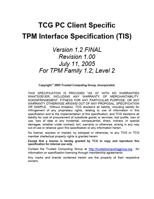
转载黑苹果集成显卡Intel HD Graphics 4400/4600 驱动方法Mobile, Intel, 苹果, 动态, 信息显卡支持列表:设备id设备平台0x0c26移动版0x0c16移动版0x0c06移动版0x0d26移动版HD 52000x0a26移动版超级本HD 50000x0a2e移动版HD 51000x0a16移动版超级本HD 44000x0426移动版HD 46000x0416移动版HD 46000x0406移动版HD 42000x0d22HD 52000x0412HD 4600ig-platform-id信息:平台ID名称管线数端口数固定显存(M)动态显存(M)端口类型成功案例0x0000060c SDV MobileGT133641024eDP, DVI,HDMI0x0000160c SDV MobileGT233641024eDP, DVI, HDMI部分hd46000x0000260c SDV MobileGT333641024eDP, DVI, HDMI i5-4570hd46000x00000604Mobile GT133641024eDP, DVI, HDMI0x00001604Mobile GT233641024eDP, DVI, HDMI0x00002604Mobile GT333641024eDP, DVI, HDMI0x0000260d CRWMobile GT333641024eDP, DVI, HDMI0x0000160a ULT Mobile GT233641024eDP, DVI, HDMI i5-4500uhd44000x0000260a ULTMobile GT333641024eDP, DVI, HDMI0x02001604Mobile GT211641024eDP0x0500260a ULT MobileGT333321024eDP, DP,DP0x0600260a ULT MobileGT333321024eDP, DP, DP i5-4200uhd44000x0800260a ULT MobileGT333641024eDP, DP,Thunderbolt0x08002e0a ULT reservedGT333640x0700260d CRW MobileGT334641024eDP, DP, DP,HDMI0x0300220d CRW DesktopGT233641024DP, DP, DP0x04001204Desktop GT20064256无个人建议,先尝试使用参数驱动。
提升基于英特尔®架构的 Android* 模拟器的速度Costas Styliano...于星期五, 04/10/2013 - 00:21 提交摘要:如果您是一名Android* 开发人员,而且对Android 模拟器的性能不满意,请阅读本文。
我们经常听到许多Android 开发人员抱怨模拟器速度缓慢而且难以操作,但是事实并不应该如此!如果您使用的是采用英特尔®处理器且支持英特尔®虚拟化技术并运行Microsoft Windows* 或Apple Mac OS* 的新电脑,那么您可以使用英特尔®硬件加速执行管理器(英特尔® HAXM)或KVM for Linux* 来轻松地大幅提升Android 模拟器的性能,进而加快Android 应用的测试和调试速度。
本文详细介绍了加速模拟器所需的步骤以及如何对其进行操作。
然后,我们将介绍如何使用NDK 编译x86 原生代码以及如何将包含x86 原生库的APK 提交至Google Play 商店。
英特尔HAXM 还可用于加速Tizen* 模拟器,但这不在本文的讨论范围之内。
如欲获取更多信息,请访问,了解SDK 部分的内容。
目录1. 简介2. 安装2.1. 前提条件2.2. 在Windows 上安装2.3. 在Linux 上安装2.3.1. KVM 安装2.4. 创建AVD(Android* 虚拟设备)3. 公认的最佳方法3.1. 在Eclipse 中使用模拟器测试应用3.2. 提交多种面向不同ABI 的APK 与提交fat 二进制文件至Google Play3.3. 编译面向x86 的NDK3.3.1. 将NDK 路径添加至环境变量3.3.2. 使用NDK 编译3.3.3. 使用NDK 编译的其他方法1. 简介本文将为您安装英特尔®硬件加速执行管理器(英特尔® HAXM)提供指导。
英特尔® HAXM 是一款硬件辅助虚拟化引擎(管理程序),它可通过英特尔®虚拟化技术(英特尔® VT)在Windows* 上加快Android* 开发速度。
LTP工具说明1LTP测试套件 (3)1.1简介 (3)1.2源目录结构 (3)2LTP安装 (4)2.1下载 (4)2.2编译 (4)2.3安装说明 (5)3LTP测试套件结构说明 (6)3.1概述 (6)3.2目录介绍 (6)3.3LTP执行原理 (6)4LTP测试套件测试内容 (7)4.1LTP测试套件测试内容 (7)4.1.1commands (7)4.1.2kernel (7)4.1.3kdump (8)4.1.4network (8)4.1.5realtime (8)4.1.6open_posix_testsuite (8)4.1.7misc (8)4.2测试方法说明 (8)4.2.1commands模块内容描述及实现方法 (8)4.2.2kernel (10)4.2.3network (15)4.2.4open_posix_testsuite (17)4.2.5realtime (18)5LTP测试套件配置详细 (19)5.1networktests.sh脚本配置 (19)5.2networkstress.sh配置 (23)5.3open_posix_testsuite测试套件 (28)5.4realtime配置 (29)5.5mm脚本的配置 (30)5.6io脚本配置 (30)5.7filecaps的配置 (30)5.8tpm_tools的配置 (31)5.9tcore的配置 (31)5.10io_floppy的配置 (31)5.11io_cd 的配置 (32)5.12cpuhotplug的配置 (32)5.13adp.sh的配置 (33)5.14autofs1.sh和autofs4.sh的配置 (34)5.15exportfs.sh的配置 (34)5.16isofs.sh的配置 (34)5.17ltpdmmapper.sh的配置 (35)5.18ltpfslvm.sh的配置及要求 (36)5.19ltpfsnolvn.sh的配置及要求 (36)5.20ltp-scsi_debug.sh的配置及要求 (37)5.21sysfs.sh的配置及要求 (37)5.22rpctirpc的配置及要求 (37)5.23test_selinux.sh的配置及要求 (39)5.24smack的配置和要求 (40)5.25perfcounters的配置及要求 (41)5.26can的配置及要求 (41)5.27test_robind.sh的配置 (42)6LTP测试套件使用说明 (43)6.1概述 (43)6.2测试方法 (44)6.2.1初始测试 (44)6.2.2压力测试 (47)1LTP测试套件1.1简介LTP(Linux Test Project)是SGI、IBM、OSDL和Bull合作的项目,目的是为开源社区提供一个测试套件,用来验证Linux系统可靠性、健壮性和稳定性。


Federal Communications Commission (FCC) Statement (011898)This equipment has been tested and found to comply with the limits for a Class B digital device, pursuant to Part 15 of FCC Rules. These limits are designed to provide reasonable protection against harmful interference in a residential installation. This equipment generates, uses and can radiate radio frequency energy and, if not installed and used in accordance with instructions contained in this manual, may cause harmful interference to radio and television communications. However, there is no guarantee that interference will not occur in a particular installation.If this equipment does cause harmful interference to radio or television reception, which can be determined by turning the equipment off and on, the user is encouraged to try to correct the interference by one or more of the following measures:-REORIENT OR RELOCATE THE RECEIVING ANTENNA-INCREASE THE SEPARATION BETWEEN THE EQUIPMENT AND THE RECEIVER -CONNECT THE EQUIPMENT INTO AN OUTLET ON A CIRCUIT DIFFERENT FROM THAT OF THE RECEIVER-CONSULT THE DEALER OR AN EXPERIENCED AUDIO/TELEVISION TECHNICIANNOTE:Connecting this device to peripheral devices that do not comply with Class B requirements, or using an unshielded peripheral data cable, could also result in harmful interference to radio or television reception.The user is cautioned that any changes or modifications not expressly approved by the party responsible for compliance could void the user’s authority to operate this equipment.To ensure that the use of this product does not contribute to interference, it isnecessary to use shielded I/O cables.CopyrightThis manual is copyrighted with all rights reserved. No portion of this manual may be copied or reproduced by any means.While every precaution has been taken in the preparation of this manual, no responsibility for errors or omissions is assumed. Neither is any liability assumed for damages resulting from the use of the information contained herein.TrademarksAll brand names, logos and registered trademarks mentioned are property of their respective owners.Table of ContentsHARDWARE CONFIGURATION (3)Key Features (3)Motherboard Layout (5)Jumper Settings (6)CPU Speed Selection (6)SW1, SW2 - CPU Frequency Ratio (6)SW3 - VID[0:4] Code to Voltage Definition (7)J7 - CMOS Clear (8)J2 - On Board AC97 Codec Sound (8)Pin Assignment (9)HARDWARE SETUP (10)T o Install DIMMs (10)Installing a New Processor (11)To Install a Processor to ZIF Socket (11)Connect the processor Fan Connector (11)BIOS SETUP (12)Starting Setup (12)Main Menu (13)Standard CMOS Features (14)Advanced BIOS Features (16)Advanced Chipset Features (16)Integrated Peripherals (16)Power Management Setup (16)PnP/PCI Configurations (16)PC Health Status (16)Frequency/Voltage Control (16)Set Supervisor/User Password (16)Flash Update Procedure (18)APPENDIX (19)Select the Heatsink (19)Select the Power Supply (20)HARDWARE CONFIGURATIONKey Features:Chipset•VIA® KT133/KT133A Chipset.Processor•Full support for the AMD Duron TM and Athlon TM processors using Socket A.•Supports 100MHz & 133MHz (optional) bus speed including all processors using Socket A.VRM 9.0 (Voltage Regulator Modules) on Board•Flexible motherboard design with on board VRM 9.0.System Memory• A total of three 168-pin DIMM sockets (3.3V Synchronous DRAM).•Supports Synchronous DRAM PC100/PC133.•Memory size up to 1.5G bytes.•Supports SDRAM memory types.•Supports single-density DIMMs of 1MB, 2MB, 4MB, 8MB and 16MB depth (x64).•Supports double-density DIMMs of 2MB, 4MB, 8MB, 16MB and 32MB depth (x64).•Supports single & double sided DIMMs.•Banks of different DRAM types depths can be mixed.System BIOS•2MB flash BIOS supporting PnP, APM, ATAPI and Windows® 95.•Auto detects and supports LBA hard disks with capacities up to 8.4GB.•Full support of ACPI & DMI.•Easy to upgrade BIOS by end-user.Dual BIOS•As our dual BIOS use the awdflash ver.7.83 to flash the dual BIOS, so our dual BIOS support the flash type of the awdflash ver.7.83, such as Syncmos,ATMEL etc..•The normal boot sequence is from main BIOS. If one BIOS is fail to boot, you can press the ‘Reset’ button to boot from the other BIOS (Note: no every time issuccess, you can try it several times or touch button time is enough long, forexample 2~3 second).•If the BIOS error that contained in compressed part of BIOS bin file, our dual BIOS can know to automatic flash, but the boot block error can not know to flash, that is: If the BIOS bin file is damage, it will auto flash BIOS, and if the bin file is OKeven different with the board bin file, computer will boot normal without enter the flash screen). If the user want to flash the BIOS unconditionally, you can press the ‘Alt + F2’ key to flash another BIOS.On-board I/O•On board two PCI fast IDE ports supporting up to 4 ATA and Ultra DMA33/66/ 100 (optional) IDE devices.•Supports bus master IDE, PIO mode 4 (up to 16.6M bytes/sec) and Ultra DMA33/66/100 (optional) (up to 33/66/100M (optional) bytes/sec) transfer.•One ECP/EPP parallel port.•Two 16550-compatible UART serial ports.•One floppy port, supports two FDDs of 360KB, 720KB, 1.2MB, 1.44MB and 2.88MB capacity.•Four USB ports.•PS/2 mouse port.•PS/2 keyboard port.•Infrared (IrDA) is supported.•One Line/Speaker out, one Mic in, one Line in and MIDI/Game port (optional).Plug-and-Play•Supports plug-and-play specification 1.1.•Plug-and-play for DOS, Windows® 3.X, Windows® 95 as well as Windows® 98.•Fully steerable PCI interrupts.On-board AC97 Sound•Integrated AC97 controller with standard AC97 codec.•Direct Sound and Sound Blaster compatible.•Full-Duplex 16-bit record and playback.•PnP and APM 1.2 support.On-board Creative Sound (optional)•Creative ES1373 Audio controller.•128 voice wave table synthesizer.•DOS game compatibility.•PCI bus master for fast DMA.•Fully compliant with PC97 power management specification.(Note: If Creative PCI Sound is on board, only Primary AMR Card can be used. If Creative PCI Sound is enabled, Bus Master Device on one PCI cannot be used.)Power Management•Supports SMM, APM and ACPI.•Break switch for instant suspend/resume on system operations.•Energy star “Green PC” compliant .•WOL (Wake-On-Lan) Header support.•External Modem Ring-in Wake-up support.•Support auto setting or manual setting for CPU voltage.•Supports suspend-to-RAM (STR) (optional).Expansion Slots• 5 PCI bus master slots (Rev. 2.1 compliant).• 1 Audio Modem Riser (AMR) (optional).• 1 ISA slot (1 ISA slot share with 1 PCI slot).• 1 universal AGP slot (AGP 2.0 compliant - 4X mode support).CAUTIONStatic electricity can harm delicate components of the motherboard. To prevent damage caused by static electricity, discharge the static electricity from yourbody before you touch any of the computers electronic components.Motherboard LayoutThe following diagrams show the relative positions of the jumpers, connectors, major components and memory banks on the motherboard.# The AMR slot is optional.NOTE1)Be sure to check the cable orientation in order to match the colored strip tothe pin 1 end of the connector.2)When you start up the system, please wait for 5 seconds after you poweron AC.Jumper SettingsThis chapter explains how to configure the motherboard’s hardware. Before using your computer, make sure all jumpers and DRAM modules are set correctly. Refer to this chapter whenever in doubt.CPU Speed SelectionIn this motherboard, you can set the CPU speed by manual or auto way, but over clock isn’t recommended.SW1, SW2 - CPU Frequency RatioSW2[1:5]SW1[1:4] SW2[1:5] CPU FREQ1 2 3 4 5SW3 - VID[0:4] Code to Voltage DefinitionSW1(6) Off, Auto Setting SW1(6) On, Manual Setting。


Intel USB4 Evaluation Dock Update ManualINFORMATION IN THIS DOCUMENT IS PROVIDED IN CONNECTION WITH INTEL® PRODUCTS. NO LICENSE, EXPRESS OR IMPLIED, BY ESTOPPEL OR OTHERWISE, TO ANY INTELLECTUAL PROPERTY RIGHTS IS GRANTED BY THIS DOCUMENT. EXCEPT AS PROVIDED IN INTEL'S TERMS AND CONDITIONS OF SALE FOR SUCH PRODUCTS, INTEL ASSUMES NO LIABILITY WHATSOEVER, AND INTEL DISCLAIMS ANY EXPRESS OR IMPLIED WARRANTY RELATING TO SALE AND/OR USE OF INTEL PRODUCTS, INCLUDING LIABILITY OR WARRANTIES RELATING TO FITNESS FOR A PARTICULAR PURPOSE, MERCHANTABILITY, OR INFRINGEMENT OF ANY PATENT, COPYRIGHT, OR OTHER INTELLECTUAL PROPERTY RIGHT.A "Mission Critical Application" is any application in which failure of the Intel Product could result, directly or indirectly, in personal injury or death. SHOULD YOU PURCHASE OR USE INTEL'S PRODUCTS FOR ANY SUCH MISSION CRITICAL APPLICATION, YOU SHALL INDEMNIFY AND HOLD INTEL AND ITS SUBSIDIARIES, SUBCONTRACTORS AND AFFILIATES, AND THE DIRECTORS, OFFICERS, AND EMPLOYEES OF EACH, HARMLESS AGAINST ALL CLAIMS COSTS, DAMAGES, AND EXPENSES AND REASONABLE ATTORNEYS' FEES ARISING OUT OF, DIRECTLY OR INDIRECTLY, ANY CLAIM OF PRODUCT LIABILITY, PERSONAL INJURY, OR DEATH ARISING IN ANY WAY OUT OF SUCH MISSION CRITICAL APPLICATION, WHETHER OR NOT INTEL OR ITS SUBCONTRACTOR WAS NEGLIGENT IN THE DESIGN, MANUFACTURE, OR WARNING OF THE INTEL PRODUCT OR ANY OF ITS PARTS.Intel may make changes to specifications and product descriptions at any time, without notice. Designers must not rely on the absence or characteristics of any features or instructions marked "reserved" or "undefined". Intel reserves these for future definition and shall have no responsibility whatsoever for conflicts or incompatibilities arising from future changes to them. The information here is subject to change without notice. Do not finalize a design with this information.The products described in this document may contain design defects or errors known as errata which may cause the product to deviate from published specifications. Current characterized errata are available on request. Contact your local Intel sales office or your distributor to obtain the latest specifications and before placing your product order. Copies of documents which have an order number and are referenced in this document, or other Intel literature, may be obtained by calling 1-800-548-4725, or goto: /design/literature.htm.All information provided related to future Intel products and plans is preliminary and subject to change at any time, without notice.Intel and the Intel logo are trademarks or registered trademarks of Intel Corporation or its subsidiaries in the United States and other countries.* Other names and brands may be claimed as the property of others.Copyright © 2020, Intel Corporation. All rights reserved.Important: Intel USB4 Evaluation Dock should be Powered off (No Power Supply must be Connected to the Board) when updating FW1.Equipment:1.1Dediprog SF600 (used to update the following components on the Intel USB4 EvaluationDock):Goshen Ridge: U8 – GR NVMDelta Bridge: UB10 – DB NVMUSB2.0 Hub: UB6 – USB2 HUB NVMFigure 1: Dediprog SF600SF600 SPI NOR Flash Programmer-Reference Link:https:///product/SF600-Link for downloading software:https:///download?productCategory=SPI+Flash+Solution&productName=SF600+SPI+NOR+Flash+Programmer&fileType=10Figure 2: Test ClipISP Testclip (SO8) (Compatible with SF100)Model Name: ISP-TC-8ISP Testclip (SO8) (Compatible with SF100)Reference Link: https:///product/ISP-TC-81.2Cypress MiniProg4 Program and Debug Kit CY8CKIT – 005 (used for updating thefollowing components):Cypress DMC (J5)Cypress CCG5(J4).Figure 3: Cypress MiniProg4 Program and Debug Kit CY8CKIT – 005-Reference Link: https:///product-detail/en/CY8CKIT-005/428-4713-ND/10314122?utm_medium=email&utm_source=oce&utm_campaign=3103_OCE20 RT&utm_content=productdetail_US&utm_cid=457843&so=64303907&mkt_tok=ey JpIjoiTURjNVlXVTBOekV4TW1aaSIsInQiOiJabjNuUjdzczgxZ0NCdWJBbExnR2k 3czkxNjhhZUVRcEFRdjlGSEZzeVZNNzdHcDRBSnEyYzhwa1F4QUJWS1NUeTJ wcEtXV1Z6d2tlbnpQbHUxamJCU1hqUHNhd3I4c1ZBaEd0WWtBUklLc0VsZ3F5T nc2eVRsYkZubXJrTm14dyJ9-Link for downloading software (Name of software: Download PSoC Programmer3.x.x.exe):https:///documentation/software-and-drivers/psoc-programmer-archiveNote: You need to create an account to able to download softwareNote: You need buy 5 Female to Male External Jumper for connecting.Figure 4: Female To Male Jumper-Reference Link: https:///GenBasic-Female-Solderless-Breadboard-Prototyping/dp/B077N7J6C4/ref=sr_1_7?dchild=1&keywords=male+to+female+jumper+wires&qid=1600894633&sr=8-7ponent Side and Back Side of Intel USB4 Evaluation DockFigure 5: Intel USB4 Evaluation Dock Component SideGR JTAG PA (UFP)DBR JTAGGR NVMCCG5 SWD Headers DMC SWD HeadersTMU CLKOUTFigure 6: Intel USB4 Evaluation Dock Back SideUB6 –USB2 HUB NVM UB10 – DB NVM Pin 0Pin 0Intel USB4 Evaluation Dock BKC File exampleGoshen Ridge: GR_4C_A0_rev9_ GATKES_BOARD.binDelta Bridge: DBR_CDR_ON_BOARD_rev1_NOSEC_sign.binFresco Hub: UB6_RegisterOnly_AddHeader_Merged_INTEL_1U5D_FL5801_1Q1_V02Cypress PD: DMC: CY7C65219‐40LQXIT_dmc_gatkex_creek_sha_3_3_0_1746_1_3_19_120W.hex CCG5: CYPD5235‐96BZXI_gatkex_3_3_1_39_2_8_0_nb.hex3.GoshenRidge FW UpdateExample file: GR_4C_A0_rev9_ GATKES_BOARD.bin-Step 1: Plug Dediprog SF600 flasher to PC-Step 2: Open Dediprog Engineering Application:o Go to Config Menu at the Top→Select Batch Operations(Top Left)→Check the Batch Operation Options is the same as Yellow Hightlight (see Figure 7) -→everything else leave as defaultFigure 7: Batch Operation Options- Step 3: Open U8 – NVM and take out the chip inside (see Figure 8)Figure 8: Chip inside U8 NVM- Step 4: Connect the SPI flash component to flasher (chip inside U8).Note: Make sure pin 0 of the chip is at the white line of the clip (see Figure 9)Figure 9: Connect the SPI Flash component to flasher (U8)- Step 5: Detect → choose First Chip number in the Memory list. (See Figure 10)- Note: If you do not see Memory list after Detect Chip → Please check the Connection between Chip and Test Clip-→Make sure they are connected correctlyPin 0Figure 10: Choose the chip from memory listNote: Majority of the time, the first component in the list is the correct chip.-Step 6: File load Goshen Ridge FW from BKC file bin file (See Figure 11), Select OKFigure 11: Load Intel USB4 Evaluation Dock bin file-Step 7: Batch-Step 8: Wait for all stages are PASS(see Figure 12), and Operation CompletelyFigure 12: All stages are PASSNote:-All stages are PASS only if you choose the correct chip in step 5.-In case you choose the wrong chip in step 5, you will see the following messageFigure 13: Error message after Batch when we choose the wrong chip Troubleshoot:-At Step 5: Detect → choose Second Chip number(W25Q168) of component in the list -Repeat Step 6 to Step 8-If Error:Programming Fail Message still occur→ At Step 5: Detect → choose Third Chip number (W25Q16CL)-Repeat Step 6 to Step 8-Step 9: Put the chip back to U8 GR NVM. Make sure pin 0 is on arrow position of U8 GR NVM .-Figure 14: Arrow Position of U8 GR NVM. Pin0 of Chip will go here4. Delta Bridge FW UpdateExample File: DBR_CDR_ON_BOARD_rev1_NOSEC_sign.bin Delta Bridge FW will be updated into UB10 componentFigure 15: Pin 0 at UB10While Dediprog SF600 flasher connected to PC and Dediprog application open:- Step 1: Connect the SPI flash component to flasher (UB10). Make sure the white linein the test clip connect to pin 0 (see Figure 16)Figure 16: Connect the SPI flash component to UB10-Step 2: Detect → choose First Chip number in the Memory list. (See Figure 17) -Note: If you do not see Memory list after Detect Chip→ Please check Connectionbetween Chip and Test Clip → Make sure they are connected correctlyFigure 17: Choose the chip from memory listNote: For most of the time, the first component in the list is a correct chip.-Step 3: File load Delta Bridge FW from BKC file bin file (See Figure 18)Figure 18: Load Intel USB4 Evaluation Dock bin file-NOTE:You may need to hold test clip to make sure test clip and chip connected. -Step 4: Batch-Step 5: Wait for all stages are PASS (see Figure 19) and Operation Completed.Figure 19: All stages are PASSNote:-All stages are PASS only if you choose the correct chip in step 2.-In the case you choose the wrong chip in step 2, you will see the following messageFigure 20: Error message after Batch when we choose the wrong chip-Troubleshoot:-At Step 3: Detect → choose Second Chip number (W25Q80) of component in the list -Repeat Step 3 to Step 5-If Error:Programming Fail Message still occur→ At Step 2: Detect → choose Third Chip number(W25Q80BL)-Repeat Step 3 to Step 55. Fresco Hub FW UpdateExample File:UB6_RegisterOnly_AddHeader_Merged_INTEL_1U5D_FL5801_1Q1_V02 Fresco Hub FW Update into UB6 componentFigure 21: Pin 0 at UB6While Dediprog SF600 flasher connected to PC and Dediprog application open:- Step 1: Connect the SPI flash component to flasher (UB6). Make sure the white line in the clip connect to bit 0.- Step 2: Detect → choose First Chip number in the Memory list. (See Figure 22) - Note: If you do not see Memory list after Detect Chip → Please check Connectionbetween Chip and Test Clip →Make sure they are connected correctlyFigure 22: Choose the chip from memory listNote: For most of the time, the first component in the list is the correct chip.-Step 3: File load Fresco USB Hub FW from BKC file bin file (See Figure 23)Figure 23: Load Intel USB4 Evaluation Dock bin file-NOTE:You may need to hold test clip to make sure test clip and chip connected. -Step 4: Batch-Step 5: Wait for all stages are PASS (see Figure 24), and Operation CompletelyFigure 24: All stages are PASSNote:-All stages are PASS only if you choose the correct chip in step 2.-In the case you choose the wrong chip in step 2, you will see the following messageFigure 25: Error message after Batch when we choose the wrong chip -Troubleshoot:-At Step 3: Detect → choose Second Chip number(W25Q168) of component in the list -Repeat Step 3 to Step 5-If Error: Programming Fail Message still occur→ At Step 2: Detect → choose Third Chip number(W25Q16CL)-Repeat Step 3 to Step 56. Cypress DMC FW UpdateExample DMC: CY7C65219‐40LQXIT_dmc_gatkex_creek_sha_3_3_0_1746_1_3_19_120W.hex Example CCG5: CYPD5235‐96BZXI_gatkex_3_3_1_39_2_8_0_nb.hex- Step 1: Plug Cypress MiniProg4 Program and Debug Kit CY8CKIT to the PC - Step 2: Connect MiniProg4 to DMC SWD connector (J5).Note: Only flash to the top five header pins of DMC SWD-- - - -Figure 26: DMC Headers (pin 6 to pin 10)-- Note: Make sure jumper connected to SWDIO pin of Cypress MiniProg4 connect toPin 10 at DMC header Cypress Minipro4 PinIntel USB4 Evaluation Dock DMCHeader PinSWDIO Pin 10 SWCLK Pin 9-CLK XRES Pin 8-XRES GND Pin 7-GND VTARG Pin 6-VDD-Step 3: Open Cypress PSOC programmerFigure 27: Cypress PSOC programmerNote: Make sure you see MiniProg4 in Port Selection-Step 4: Load file – DMC FW hex file (It may be inside PD folder from BKC file)Figure 28: Load file-Step 5: ProgramFigure 29: Select program on PSOC Programmer-Step 6: Wait until everything is PASSFigure 30: Wait until everything is PASSNote: If you see FAIL message, you may get the connection wrong between Cypress MiniProg4 and DMC header→ Check connection again at Step 2If connection between Cypress MiniProg4 and DMC header are correct but still get FAIL message→Close PSOC Programmer application and detach/attach MiniProg4 to host and reopen PSOC Programmer.7.Cypress CCG5 FW UpdateCCG5ABCCG5CDFigure 31: CCG5 SWD (J4) ConnectorWhile Cypress MiniProg4 Program and Debug Kit CY8CKIT connected to the PCand Cypress PSOC programmer open:Update CCG5 AB:-Step 1: Connect Cypress MiniProg4 to first CCG5 AB (J4) connectorCypress Minipro4 Pin Intel USB4 Evaluation Dock DMCHeader PinSWDIO Pin 10SWCLK Pin 9XRES Pin 8GND Pin 7VTARG Pin 6--Step 2: Load file – CCG5 FW hex file-Step 3: Program-Step 4: Wait until everything is PASSUpdate CCG5 CD:-Step 1: Connect Cypress MiniProg4 to first CCG5 CD (J4) connectorCypress Minipro4 Pin Intel USB4 Evaluation Dock DMCHeader PinSWDIO Pin 1SWCLK Pin 2XRES Pin 3GND Pin 4VTARG Pin 5-Step 2: Load file – CCG5 FW hex file (the same file for CCG5 AB update)-Step 3: Program-Step 4: Wait until everything is PASSNote: There is only 1 CCG5 file for CCG5 AB and CCG5 CDNote: If you see FAIL message, you may get connection wrong between CypressMiniProg4 and DMC header→ Check connection again at Step 1If connection between Cypress MiniProg4 and DMC header are correct but still get FAIL message→Close PSOC Programmer application and detach/attach MiniProg4 to host and reopen PSOC Programmer.-Step 5: Power Intel USB4 Evaluation Dock。
CCS教程(DSP开发软件)第一章 CCS概述 (1)1.1CCS概述 (1)1.2代码生成工具 (3)1.3CCS集成开发环境 (5)1.3.1 编辑源程序 (5)1.3.2创建应用程序 (6)1.3.3 调试应用程序 (6)1.4DSP/BIOS插件 (7)1.4.1 DSP/BIOS 配置 (7)1.4.2 DSP/BIOS API 模块 (8)1.5硬件仿真和实时数据交换 (10)1.6第三方插件 (13)1.7CCS文件和变量 (14)1.7.1安装文件夹 (14)1.7.2文件扩展名 (14)1.7.3环境变量 (15)1.7.4增加DOS环境空间 (16)第二章开发一个简单的应用程序 (17)2.1创建工程文件 (17)2.2向工程添加文件 (19)2.3查看源代码 (21)2.4编译和运行程序 (23)2.5修改程序选项和纠正语法错误 (24)2.6使用断点和观察窗口 (26)2.7使用观察窗口观察STRUCTURE变量 (28)2.8测算源代码执行时间 (29)2.9进一步探索 (31)2.10进一步学习 (31)第三章开发DSP/BIOS程序 (32)3.1创建配置文件 (32)3.2向工程添加DSP/BIOS文件 (34)3.3用CCS测试 (36)3.4测算DSP/BIOS代码执行时间 (38)3.5进一步探索 (40)3.6进一步学习 (40)第四章算法和数据测试 (41)4.1打开和查看工程 (41)4.2查看源程序 (43)4.3为I/O文件增加探针断点 (45)4.4显示图形 (47)4.5执行程序和绘制图形 (48)4.6调节增益 (50)4.7观察范围外变量 (51)4.8使用GEL文件 (53)4.9调节和测试PROCESSING函数 (54)4.10进一步探索 (56)4.11进一步学习 (57)第五章程序调试 (58)5.1打开和查看工程 (58)5.2查看源程序 (60)5.3修改配置文件 (63)5.4用E XECUTION G RAPH查看任务执行情况 (66)5.5修改和查看LOAD值 (67)5.6分析任务的统计数据 (70)5.7增加STS显式测试 (72)5.8观察显式测试统计数据 (73)5.9进一步探索 (75)5.10进一步学习 (75)第六章实时分析 (76)6.1打开和查看工程 (76)6.2修改配置文件 (77)6.3查看源程序 (79)6.4使用RTDX控制修改运行时的LOAD值 (81)6.5修改软中断优先级 (84)6.6进一步探索 (85)6.7进一步学习 (85)第七章 I/O (86)7.1打开和查看工程 (86)7.2查看源程序 (87)7.3S IGNALPROG应用程序 (90)7.4运行应用程序 (91)7.5使用HST和PIP模块修改源程序 (93)7.6HST和PIP资料 (96)7.7在配置文件中增加通道和SWI (97)7.8运行修改后的程序 (100)7.9进一步学习 (100)第一章 CCS概述本章概述CCS(Code Composer Studio)软件开发过程、CCS组件及CCS使用的文件和变量。CCS提供了配置、建立、调试、跟踪和分析程序的工具,它便于实时、嵌入式信号处理程序的编制和测试,它能够加速开发进程,提高工作效率。1.1 CCS概述CCS提供了基本的代码生成工具,它们具有一系列的调试、分析能力。CCS支持如下所示的开发周期的所有阶段。在使用本教程之前,必须完成下述工作:安装目标板和驱动软件。按照随目标板所提供的说明书安装。如果你正在用仿真器或目标板,其驱动软件已随目标板提供,你可以按产品的安装指南逐步安装。安装CCS.遵循安装说明书安装。如果你已有CCS仿真器和TMS320c54X代码生成工具,但没有完整的CCS,你可以按第二章和第四章所述的步骤进行安装。运行CCS安装程序SETUP.你可以按步骤执行第二章和第四章的实验。SETUP程序允许CCS使用为目标板所安装的驱动程序。CCS包括如下各部分:CCS代码生成工具:参见1.2节CCS集成开发环境(IDE):参见1.3节DSP/BIOS插件程序和API:参见1.4节RTDX插件、主机接口和API:参见1.5节CCS构成及接口见图1-1。图1-1 CCS构成及接口1.2 代码生成工具代码生成工具奠定了CCS所提供的开发环境的基础。图1-2是一个典型的软件开发流程图,图中阴影部分表示通常的C语言开发途径,其它部分是为了强化开发过程而设置的附加功能。图1-2 软件开发流程图1-2描述的工具如下:C编译器(C compiler) 产生汇编语言源代码,其细节参见TMS320C54x最优化C 编译器用户指南。汇编器(assembler) 把汇编语言源文件翻译成机器语言目标文件,机器语言格式为公用目标格式(COFF),其细节参见TMS320C54x汇编语言工具用户指南。连接器(linker) 把多个目标文件组合成单个可执行目标模块。它一边创建可执行模块,一边完成重定位以及决定外部参考。连接器的输入是可重定位的目标文件和目标库文件,有关连接器的细节参见TMS320C54x最优化C编译器用户指南和汇编语言工具用户指南。归档器(archiver)允许你把一组文件收集到一个归档文件中。归档器也允许你通过删除、替换、提取或添加文件来调整库,其细节参见TMS320C54x汇编语言工具用户指南。助记符到代数汇编语言转换公用程序(mnimonic_to_algebric assembly translator utility)把含有助记符指令的汇编语言源文件转换成含有代数指令的汇编语言源文件,其细节参见TMS320C54x汇编语言工具用户指南。你可以利用建库程序(library_build utility)建立满足你自己要求的“运行支持库”,其细节参见TMS320C54x最优化C编译器用户指南。运行支持库(run_time_support libraries) 它包括C编译器所支持的ANSI标准运行支持函数、编译器公用程序函数、浮点运算函数和C编译器支持的I/O函数,其细节参见TMS320C54x最优化C编译器用户指南。十六进制转换公用程序(hex conversion utility) 它把COFF目标文件转换成TI-Tagged、ASCII-hex、 Intel、 Motorola-S、或 Tektronix 等目标格式,可以把转换好的文件下载到EPROM编程器中,其细节参见TMS320C54x汇编语言工具用户指南。交叉引用列表器(cross_reference lister)它用目标文件产生参照列表文件,可显示符号及其定义,以及符号所在的源文件,其细节参见TMS320C54x汇编语言工具用户指南。绝对列表器(absolute lister)它输入目标文件,输出.abs文件,通过汇编.abs文件可产生含有绝对地址的列表文件。如果没有绝对列表器,这些操作将需要冗长乏味的手工操作才能完成。1.3 CCS集成开发环境CCS集成开发环境(IDE)允许编辑、编译和调试DSP目标程序。1.3.1 编辑源程序CCS允许编辑C源程序和汇编语言源程序,你还可以在C语句后面显示汇编指令的方式来查看C源程序。集成编辑环境支持下述功能:用彩色加亮关键字、注释和字符串。以圆括弧或大括弧标记C程序块,查找匹配块或下一个圆括弧或大括弧。在一个或多个文件中查找和替代字符串,能够实现快速搜索。取消和重复多个动作。获得“上下文相关”的帮助。用户定制的键盘命令分配。1.3.2创建应用程序应用程序通过工程文件来创建。工程文件中包括C源程序、汇编源程序、目标文件、库文件、连接命令文件和包含文件。编译、汇编和连接文件时,可以分别指定它们的选项。在CCS中,可以选择完全编译或增量编译,可以编译单个文件,也可以扫描出工程文件的全部包含文件从属树,也可以利用传统的makefiles文件编译。1.3.3 调试应用程序CCS提供下列调试功能:设置可选择步数的断点在断点处自动更新窗口查看变量观察和编辑存储器和寄存器观察调用堆栈对流向目标系统或从目标系统流出的数据采用探针工具观察,并收集存储器映象 绘制选定对象的信号曲线估算执行统计数据观察反汇编指令和C指令CCS提供GEL语言,它允许开发者向CCS菜单中添加功能。1.4 DSP/BIOS 插件在软件开发周期的分析阶段,调试依赖于时间的例程时,传统调试方法效率低下。DSP/BIOS插件支持实时分析,它们可用于探测、跟踪和监视具有实时性要求的应用例程,下图显示了一个执行了多个线程的应用例程时序。图1-3 应用例程中各线程时序DSP/BIOS API 具有下列实时分析功能:程序跟踪(Program tracing)显示写入目标系统日志(target log)的事件,反映程序执行过程中的动态控制流。性能监视(Performance monitoring)跟踪反映目标系统资源利用情况的统计表,诸如处理器负荷和线程时序。文件流(File streaming)把常驻目标系统的I/O对象捆绑成主机文档。DSP/BIOS 也提供基于优先权的调度函数,它支持函数和多优先权线程的周期性执行。1.4.1 DSP/BIOS 配置在CCS环境中,可以利用DSP/BIOS API定义的对象创建配置文件,这类文件简化了存储器映象和硬件ISR矢量映象,所以,即使不使用DSP/BIOS API 时,也可以使用配置文件。配置文件有两个任务:设置全局运行参数。可视化创建和设置运行对象属性,这些运行对象由目标系统应用程序的DSP/BIOS API函数调用,它们包括软中断,I/O管道和事件日志。在CCS中打开一个配置文件时,其显示窗口如下:DSP/BIOS对象是静态配置的,并限制在可执行程序空间范围内,而运行时创建对象的API调用需要目标系统额外的开销(尤其是代码空间)。静态配置策略通过去除运行代码能够使目标程序存储空间最小化,能够优化内部数据结构,在程序执行之前能够通过确认对象所有权来及早地检测出错误。保存配置文件时将产生若干个与应用程序联系在一起的文件,这些文件的细节参见1.7.2。1.4.2 DSP/BIOS API 模块传统调试(debuging)相对于正在执行的程序而言是外部的,而DSP/BIOS API要求将目标系统程序和特定的DSP/BIOS API模块连接在一起。通过在配置文件中定义DSP/BIOS 对象,一个应用程序可以使用一个或多个DSP/BIOS模块。在源代码中,这些对象声明为外部的,并调用DSP/BIOS API功能。每个DSP/BIOS模块都有一个单独的C头文件或汇编宏文件,它们可以包含在应用程序源文件中,这样能够使应用程序代码最小化。为了尽量少地占用目标系统资源,必须优化(C和汇编源程序)DSP/BIOS API调用。DSP/BIOS API划分为下列模块,模块内的任何API调用均以下述代码开头。CLK。片内定时器模块控制片内定时器并提供高精度的32位实时逻辑时钟,它能够控制中断的速度,使之快则可达单指令周期时间,慢则需若干毫秒或更长时间。HST。主机输入/输出模块管理主机通道对象,它允许应用程序在目标系统和主机之间交流数据。主机通道通过静态配置为输入或输出。HWI。硬件中断模块提供对硬件中断服务例程的支持,可在配置文件中指定当硬件中断发生时需要运行的函数。IDL。休眠功能模块管理休眠函数,休眠函数在目标系统程序没有更高优先权的函数运行时启动。LOG。日志模块管理LOG对象,LOG对象在目标系统程序执行时实时捕捉事件。开发者可以使用系统日志或定义自己的日志,并在CCS中利用它实时浏览讯息。MEM。存储器模块允许指定存放目标程序的代码和数据所需的存储器段。PIP。数据通道模块管理数据通道,它被用来缓存输入和输出数据流。这些数据通道提供一致的软件数据结构,可以使用它们驱动DSP和其它实时外围设备之间的I/O通道。PRD。周期函数模块管理周期对象,它触发应用程序的周期性执行。周期对象的执行速率可由时钟模块控制或PRD_tick的规则调用来管理,而这些函数的周期性执行通常是为了响应发送或接收数据流的外围设备的硬件中断。RTDX。实时数据交换允许数据在主机和目标系统之间实时交换,在主机上使用自动OLE的客户都可对数据进行实时显示和分析,详细资料参见1.5。STS。统计模块管理统计累积器,在程序运行时,它存储关键统计数据并能通过CCS 浏览这些统计数据。SWI。软件中断模块管理软件中断。软件中断与硬件中断服务例程(ISRs)相似。当目标程序通过API调用发送SWI对象时,SWI模块安排相应函数的执行。软件中断可以有高达15级的优先级,但这些优先级都低于硬件中断的优先级。TRC。跟踪模块管理一套跟踪控制比特,它们通过事件日志和统计累积器控制程序信息的实时捕捉。如果不存在TRC对象,则在配置文件中就无跟踪模块。有关各模块的详细资料,可参见CCS中的在线帮助,或TMS320C54 DSP/BIOS 用户指南。1.5 硬件仿真和实时数据交换TI DSPs提供在片仿真支持,它使得CCS能够控制程序的执行,实时监视程序运行。增强型JTAG连接提供了对在片仿真的支持,它是一种可与任意DSP系统相连的低侵扰式的连接。仿真接口提供主机一侧的JTAG连接,如TI XSD510。为方便起见,评估板提供在板JTAG仿真接口。在片仿真硬件提供多种功能:DSP的启动、停止或复位功能向DSP下载代码或数据检查DSP的寄存器或存储器硬件指令或依赖于数据的断点包括周期的精确计算在内的多种记数能力主机和DSP之间的实时数据交换(RTDX)图1-4 RTDX系统组成CCS提供在片能力的嵌入式支持;另外,RTDX通过主机和DSP APIs提供主机和DSP之间的双向实时数据交换,它能够使开发者实时连续地观察到DSP应用的实际工作方式。在目标系统应用程序运行时,RTDX也允许开发者在主机和DSP设备之间传送数据,而且这些数据可以在使用自动OLE的客户机上实时显示和分析,从而缩短研发时间。RTDX由目标系统和主机两部分组成。小的RTDX库函数在目标系统DSP上运行。开发者通过调用RTDX软件库的API函数将数据输入或输出目标系统的DSP,库函数通过在片仿真硬件和增强型JTAG接口将数据输入或输出主机平台,数据在DSP应用程序运行时实时传送给主机。在主机平台上,RTDX库函数与CCS一道协同工作。显示和分析工具可以通过COM API与RTDX通信,从而获取目标系统数据,或将数据发送给DSP应用例程。开发者可以使用标准的显示软件包,诸如National Instruments’LabVIEW,Quinn-Curtis’ Real-Time Graphics Tools,或Microsoft Excel。同时,开发者也可研制他们自己的Visual Basic或Visual C++应用程序。图1-5 RTDX实例RTDX能够记录实时数据,并可将其回放用于非实时分析。下述样本由National Instruments’LabVIEW 软件产生。在目标系统上,一个原始信号通过FIR滤波器,然后与原始信号一起通过RTDX发送给主机。在主机上,LabVIEW显示屏通过RTDX COM API获取数据,并将它们显示在显示屏的左边。利用信号的功率谱可以检验目标系统中FIR滤波器是否正常工作。处理后的信号通过LabVIEW,将其功率谱显示在右上部分;目标系统的原始信号通过LabVIEW的FIR滤波器,再将其功率谱显示在右下部分。比较这两个功率谱便可确认目标系统的滤波器是否正常工作。RTDX适合于各种控制、伺服和音频应用。例如,无线电通信产品可以通过RTDX捕捉语音合成算法的输出以检验语音应用程序的执行情况;嵌入式系统也可从RTDX获益;硬磁盘驱动设计者可以利用RTDX测试他们的应用软件,不会因不正确的信号加到伺服马达上而与驱动发生冲突;引擎控制器设计者可以利用RTDX在控制程序运行的同时分析随环境条件而变化的系数。对于这些应用,用户都可以使用可视化工具,而且可以根据需要选择信息显示方式。未来的 TI DSPs 将增加RTDX的带宽,为更多的应用提供更强的系统可视性。关于RTDX的详细资料,请参见CCS中RTDX在线帮助。1.6 第三方插件第三方软件提供者可创建AxtiveX插件扩展CCS功能,目前已有若干第三方插件用于多种用途。1.7 CCS文件和变量本节简述CCS文件夹、CCS的文件类型及CCS环境变量。1.7.1安装文件夹安装进程将在安装CCS的文件夹(典型情况为:c:\ti)中建立子文件夹。此外,子文件夹又建立在Windows目录下(c:\windows or c:\winnt)。C:\ti包含以下目录:bin.各种应用程序c5400\bios。DSP/BIOS API的程序编译时使用的文件c5400\cgtools.Texas instruments源代码生成工具c5400\examples.源程序实例c5400\rtdx. RTDX文件c5400\tutorial.本手册中使用的实例文件cc\bin.关于CCS环境的文件cc\gel.与CCS一起使用的GEL文件docs.PDS格式的文件和指南myprojects.用户文件夹1.7.2文件扩展名以下目录结构被添加到Windows目录:ti\drivers.各种DSP板驱动文件ti\plugins.和CCS一起使用的插件程序ti\uninstall.支持卸载CCS软件的文件当使用CCS时,你将经常遇见下述扩展名文件:S使用的工程文件program.c.C程序源文件program.asm.汇编程序源文件filename.h.C程序的头文件,包含DSP/BIOS API模块的头文件filename.lib.库文件project.cmd.连接命令文件program.obj.由源文件编译或汇编而得的目标文件program.out.(经完整的编译、汇编以及连接的)可执行文件project.wks.存储环境设置信息的工作区文件,program.cdb.配置数据库文件。采用DSP/BIOS API的应用程序需要这类文件,对于其它应用程序则是可选的。保存配置文件时将产生下列文件:◆programcfg.cmd.连接器命令文件◆programcfg.h54.头文件◆programcfg.s54.汇编源文件1.7.3环境变量安装程序在autoexec.bat文件中定义以下变量(对Windows 95和98)或环境变量(对于Windows NT):表1-1 环境变量1.7.4增加DOS环境空间如果使用的是Windows 95,你可能需要增加DOS界面的环境空间,以便支持建立一个CCS 应用所需的环境变量。把下一行添加到config.sys文件中,然后重新启动计算机:shell=c:\windows\ /e:4096 /p第二章开发一个简单的应用程序本章使用hello world实例介绍在CCS中创建、调试和测试应用程序的基本步骤;介绍CCS的主要特点,为在CCS中深入开发DSP软件奠定基础。在使用本实例之前,你应该已经根据安装说明书完成了CCS安装。建议在使用CCS时利用目标板而不是仿真器。如果没有CCS而只有代码生成工具和Code Composer或者是利用仿真器在进行开发,你只要按第二章和第四章中的步骤执行即可。2.1 创建工程文件在本章中,将建立一个新的应用程序,它采用标准库函数来显示一条hello world 消息。1.如果CCS安装在c:\ti中,则可在c:\ti\myprojects建立文件夹hello1。(若将CCS安装在其它位置,则在相应位置创建文件夹hello1。)2.将c:\ti\c5400\tutorial\hello1中的所有文件拷贝到上述新文件夹。3.从Windows Start菜单中选择Programs→Code Composer Studio ‘C5400→CCStudio。(或者在桌面上双击Code Composer Studio图标。)注:CCS设置如果第一次启动CCS时出现错误信息,首先确认是否已经安装了CCS。如果利用目标板进行开发,而不是带有CD-ROM的仿真器,则可参看与目标板一起提供的文档以设置正确的I/O端口地址。4.选择菜单项Project→New。5.在Save New Project As窗口中选择你所建立的工作文件夹并点击Open。键入myhello作为文件名并点击Save,CCS就创建了myhello.mak的工程文件,它存储你的工程设置,并且提供对工程所使用的各种文件的引用。2.2 向工程添加文件1.选择Project→Add Files to Project,选择hello.c并点击Open。2.选择Project→Add Files to Project,在文件类型框中选择*.asm。选择vector.asm并点击Open。该文件包含了设置跳转到该程序的C入口点的RESET中断(c_int00)所需的汇编指令。(对于更复杂的程序,可在vector.asm定义附加的中断矢量,或者,可用3.1节上所说明的DSP/BIOS来自动定义所有的中断矢量)3.选择Project→Add Files to Project,在文件类型框中选择*.cmd。选择hello.cmd并点击Open,hello.cmd包含程序段到存储器的映射。4.选择Project→Add Files to Project,进入编译库文件夹(C:\ti\c5400\cgtools\lib)。在文件类型框中选择*.o*,*.lib。选择rts.lib并点击Open,该库文件对目标系统DSP提供运行支持。5.点击紧挨着Project、Myhello.mak、Library和Source旁边的符号+展开Project表,它称之为Project View。注:打开Project View如果看不到Project View,则选择View→Project。如果这时选择过Bookmarks图标,仍看不到Project View,则只须再点击Project View底部的文件图标即可。6.注意包含文件还没有在Project View中出现。在工程的创建过程中,CCS扫描文件间的依赖关系时将自动找出包含文件,因此不必人工地向工程中添加包含文件。在工程建立之后,包含文件自动出现在Project View中。如果需要从工程中删除文件,则只需在Project View中的相应文件上点击鼠标右键,并从弹出菜单中选择Remove from project即可。在编译工程文件时,CCS按下述路径顺序搜索文件:包含源文件的目录编译器和汇编器选项的Include Search Path中列出的目录(从左到右)列在C54X_C_DIR(编译器)和C54X_A_DIR(汇编器)环境变量定义中的目录(从左到右)。2.3 查看源代码1.双击Project View中的文件hello.c,可在窗口的右半部看到源代码。2.如想使窗口更大一些,以便能够即时地看到更多的源代码,你可以选择Option→Font使窗口具有更小的字型。/* ======== hello.c ======== */#include <stdio.h>#include "hello.h"#define BUFSIZE 30struct PARMS str ={2934,9432,213,9432,&str};/** ======== main ========**/void main(){#ifdef FILEIOint i;char scanStr[BUFSIZE];char fileStr[BUFSIZE];size_t readSize;FILE *fptr;#endif/* write a string to stdout */puts("hello world!\n");#ifdef FILEIO/* clear char arrays */for (i = 0; i < BUFSIZE; i++) {scanStr[i] = 0 /* deliberate syntax error */fileStr[i] = 0;}/* read a string from stdin */scanf("%s", scanStr);/* open a file on the host and write char array */fptr = fopen("file.txt", "w");fprintf(fptr, "%s", scanStr);fclose(fptr);/* open a file on the host and read char array */fptr = fopen("file.txt", "r");fseek(fptr, 0L, SEEK_SET);readSize = fread(fileStr, sizeof(char), BUFSIZE, fptr);printf("Read a %d byte char array: %s \n", readSize, fileStr);fclose(fptr);#endif}当没有定义FILEIO时,采用标准puts()函数显示一条hello world消息,它只是一个简单程序。当定义了FILEIO后(见2.5节),该程序给出一个输入提示,并将输入字符串存放到一个文件中,然后从文件中读出该字符串,并把它输出到标准输出设备上。2.4 编译和运行程序CCS会自动将你所作的改变保存到工程设置中。在完成上节之后,如果你退出了CCS,则通过重新启动CCS和点击Project→Open,即可返回到你刚才停止工作处。注:重新设置目标系统DSP如果第一次能够启动CCS,但接下来得到CCS不能初始化目标系统DSP的出错信息则可选择Debug→Reset DSP菜单项。若还不能解决上述问题,你可能需要运行你的目标板所提供的复位程序。为了编译和运行程序,要按照以下步骤进行操作:1.点击工具栏按钮或选择Project→Rebuild All ,CCS重新编译、汇编和连接工程中的所有文件,有关此过程的信息显示在窗口底部的信息框中。2.选择File→Load Program,选择刚重新编译过的程序myhello.out(它应该在c:\ti\myprojects\hello1文件夹中,除非你把CCS安装在别的地方)并点击Open。CCS把程序加载到目标系统DSP上,并打开Dis_Assembly窗口,该窗口显示反汇编指令。(注意,CCS还会自动打开窗口底部一个标有Stdout的区域,该区域用以显示程序送往Stdout的输出。)3.点击Dis_Assembly窗口中一条汇编指令(点击指令,而不是点击指令的地址或空白键。CCS将搜索有关那条指令的帮助信息。这是一种获得关于不熟悉的区域)。按F1汇编指令的帮助信息的好方法。4.点击工具栏按钮或选择Debug→Run。注:屏幕尺寸和设置工具栏有些部分可能被Build窗口隐藏起来,这取决于屏幕尺寸和设置。为了看到整个工具栏,请在Build窗口中点击右键并取消Allow Docking选择。当运行程序时,可在Stdout窗口中看到hello world消息。2.5 修改程序选项和纠正语法错误在前一节中,由于没有定义FILEIO,预处理器命令(#ifdef 和#endif)之间的程序没有运行。在本节中,使用CCS设置一个预处理器选项,并找出和纠正语法错误。1.选择Project→Options。2.从Build Option窗口的Compiler栏的Category列表中选择Symbles。在DefineSymbles框中键入FILEIO并按Tab键。注意,现在窗口顶部的编译命令包含-d选项,当你重新编译该程序时,程序中#ifdef FILEIO语句后的源代码就包含在内了。(其它选项可以是变化的,这取决于正在使用的DSP板。)3.点击OK保存新的选项设置。4.点击(Rebuild All)工具栏按钮或选择Project→Rebuild All。无论何时,只要工程选项改变,就必须重新编译所有文件。5.出现一条说明程序含有编译错误的消息,点击Cancel。在Build tab 区域移动滚动条,就可看到一条语法出错信息。6.双击描述语法错误位置的红色文字。注意到hello.c源文件是打开的,光标会落在该行上: fileStr[i] = 07.修改语法错误(缺少分号)。注意,紧挨着编辑窗口题目栏的文件名旁出现一个星号(*),表明源代码已被修改过。当文件被保存时,星号随之消失。8.选择File→Save 或按Ctrl+S可将所作的改变存入hello.c。9.点击(Incremental Build)工具栏按钮或选择Project→Build,CCS重新编译已被更新的文件。2.6 使用断点和观察窗口当开发和测试程序时,常常需要在程序执行过程中检查变量的值。在本节中,可用断点和观察窗口来观察这些值。程序执行到断点后,还可以使用单步执行命令。1.选择File→Reload Program.2.双击Project View中的文件hello.c。可以加大窗口,以便能看到更多的源代码。3.把光标放到以下行上:fprintf(fptr, “%S”, scacStr);4.点击工具栏按钮或按F9,该行显示为高亮紫红色。(如果愿意的话,可通过Option→Color改变颜色。)5.选择View→Watch Window。CCS窗口的右下角会出现一个独立区域,在程序运行时,该区域将显示被观察变量的值。6.在Watch Window区域中点击鼠标右键,从弹出的表中选择Insert New Expression。7.键入表达式*scanStr并点击OK。8.注意局部变量*scanStr被列在Watch window中,但由于程序当前并未执行到该变量的main()函数,因此没有定义。9.选择Debug→Run或按F5。10.在相应提示下,键入goodbye并点击OK。注意,Stdout框以蓝色显示输入的文字。还应注意,Watch Window中显示出*scanStr的值。在键入一个输入字符串之后,程序运行并在断点处停止。程序中将要执行的下一行以黄色加亮。11.点击(Step Over)工具栏按钮或按F10以便执行到所调用的函数fprintf()之后。12.用CCS提供的step命令试验:■ Step Into (F2)■ Step over (F10)■ Step Out (Shift F7)■Run to Cursor (Ctrl F10)13.点击工具栏按钮或按F5运行程序到结束。2.7 使用观察窗口观察structure变量观察窗除了观察简单变量的值以外,还可观察结构中各元素元素的值。1.在watch Window区域中点击鼠标右键,并从弹出表中选择Insert New Expression。2.键入str 作为表达式并点击OK。显示着+str={…}的一行出现在Watch Window中。
User ManualV1.1 M aster Series Embedded SystemIntel ® Tiger Lake-UP3 Core-i/Celeron Processors Performance, Versatile, and Rugged & ReliablePREFACECopyright NoticeCopyright © 2016-2021 MiTAC Computing Technology Corporation (MiTAC Group). No part of this document may be reproduced, copied, translated, or transmitted in any form or by any means, electronic or mechanical, for any purpose, without the prior written permission of MiTAC Corp., Ltd. All information and specification provided in this manual are for reference only and remain subject to change without prior notice.DisclaimerWe reserve the right to make changes, without notice, to any product, including circuits and/or software described or contained in this manual in order to improve design and/or performance. We assume no responsibility or liability for the use of the described product(s) conveys no license or title under any patent, copyright, or masks work rights to these products, and make no representations or warranties that these products are free from patent, copyright, or mask work right infringement, unless otherwise specified. Applications that are described in this manual are for illustration purposes only. We make no representation or guarantee that such application will be suitable for the specified use without further testing or modification.Declaration of ConformitySafety InformationSafety PrecautionsFor your safety, please carefully read all the safety instructions before using the device. All cautions and warnings on the equipment should be noted. Keep this user manual for future reference.*Let service personnel to check the equipment in case any of the following problems appear:⏹The power cord or plug is damaged.⏹Liquid has penetrated into the equipment.⏹The equipment has been exposed to moisture.⏹The equipment does not work well or you cannot get it to work according to the user manual.⏹The equipment has been dropped and damaged.⏹The equipment has obvious signs of breakage on the surface.Ordering InformationPacking ListOptional Xpansion Modules and AccessoriesCONTENTSPREFACE 1CHAPTER 1: INTRODUCTION (10)1.1 Overview (10)1.2 Product Features (10)1.3 Hardware Specification (11)1.4 Mechanical Specification (15)1.5 System I/O Placement (16)CHAPTER 2: DIP SWITCH SETTING AND PIN DEFINITION (20)2.1 Jumper and Internal Connector Overall Placement (20)2.2 Jumper Setting (22)2.3 Internal Connector Pin Definition (24)2.4 External Connector Pin Definition (27)2.5 Xpansion Module MS-48CDN-DT10 (30)2.6 Xpansion Module MS-04LAN-M10 (34)2.7 Xpansion Module MS-01IGN-S10 (35)CHAPTER 3: SYSTEM SETUP (37)CHAPTER 4: BIOS SETUP (40)4.1 Main Page (40)4.2 Advanced Page (42)4.3 Evnet logs (58)4.4 Security Page (61)4.5 Boot Page (69)4.6 Save & Exit Page (73)1 INTRODUCTIONThis chapter provides the MP1-11TGS EmbeddedSystem product overview, including features,hardware and mechanical specifications.CHAPTER 1: INTRODUCTIONThis chapter provides the MP1-11TGS Embedded System product overview, including features, hardware, mechanical specifications, and I/O placement.1.1 OverviewMiTAC’s MP1-11TGS embedded system is the next generation embedded system with Intel® 11st Gen. (10nm+ manufacturing process) Tiger Lake-UP3 processor which integrates Iris Xeoutstanding graphic engine. The excellent graphic performance, performance processor, OCP/OVP power protection, and expandable design provide the solution for every complicated task and most types of application.1.2 Product FeaturesMP1-11TGS Embedded System offers the following features:⏹11st Generation Intel® Tiger Lake-UP3 Co re™ i7 / i5 / i3 / Celeron Processors⏹Integrated Intel® Iris Xe Graphic Engine⏹Quadruple Display with HDMI and DisplayPort Interface⏹Fan-less chassis and Expandable module design⏹Support COM/DIO/LAN/PoE via Xpansion Modules (Only for MP1-D model)⏹Support Power Ignition for Vehicle Application via Xpansion Module (Only for MP1-Dmodel)⏹8-24V Wide Power Voltage for MP1-11TGS; 12-36V Wide Power Voltage forMP1-11TGS-D⏹15W TDP: -40 ~ 70°C28W TDP: -40 ~ 60°C*with 0.7m/s Air Flow (w/ Extended Temp. SSD/mSATA/RAM)1.3 Hardware Specification*Notes1: Installation in Restricted Access Location (RAL)A restricted access location is a designated area within an incident area (High or Low temperature environment)With authorized people can enter for a period of time and for a specific purpose.1.Access can only be gained by service people or by users who have beeninstructed about the reasons for the Restrictions applied to the location and about any precautions that shall be taken.2.Access is through the use of a tool or lock and key, or other means ofsecurity, and is controlled by the authority Responsible for the location.*Notes2: Please make sure that the power consumption is in the spec of the power supply output capability from AC adaptor (72W or 120W). Please choose the suitable AC adaptor for your application.AC/DC 24V/3A, 72W 3PIN Terminal Block Power AdaptorAC/DC 24V/5A, 120W 3PIN Terminal Block Power Adaptor*Note3: The safety ambient operating temperature is 40 degree C if the external AC adapter model: EA10681V or EA11011M will be placed in thesame high temperature area with the embedded system.*Note4: In the PXE application, please install i219-LM driver in OS image inadvance before installing OS via PXE server.*Note5: CAUTION - Lithium battery is included in this embedded system. Please do not puncture, mutilate, or dispose of battery in fire. There will be danger of explosion if battery is incorrectly replaced. Replace only with the same or equivalent type recommended by manufacturer. Dispose of used battery according to manufacturer instructions and in accordance with your local regulations.1.4 Mechanical SpecificationMP1-11TGS⏹Mechanical Dimension: 210 mm x 150 mm x 63 mmMP1-11TGS-D⏹Mechanical Dimension: 210 mm x 150 mm x 103 mm1.5 System I/O PlacementMP1-11TGS⏹Front I/O:⏹Rear I/O:MP1-11TGS-D ⏹Front I/O:⏹Rear I/O:Xpansion Module (Optional) Configuration Table MP1-11TGSMP1-11TGS-D2 DIP SWITCH SETTING AND PIN DEFINITIONThis chapter provides information about how to set up thedip switch and use internal I/Os of MP1-11TGS EmbeddedSystem hardware.CHAPTER 2: DIP SWITCH SETTING AND PIN DEFINITIONThis chapter provides information about how to set up the dip switch, and use internal I/Os of MP1-11TGS Embedded System hardware.2.1 Jumper and Internal Connector Overall Placement2.2 Jumper Setting2.3 Internal Connector Pin Definition Standard ConnectorsSpecial Connectors2.4 External Connector Pin Definition⏹COM#1-3 (RS232) / COM#4 (RS232/422/485)⏹3-pin terminal block for DC Input*Only available in MP1-11TGS-D model.4-pin terminal block for DC Output (for MP1-11TGS-D model only)2.5 Xpansion Module MS-48CDN-DT10This Module MS-48CDN-DT10 consists of two parts, one is Serial COM, and the other is Digital IO function.Please see the guideline about how to set up this Module correctly.COM Port Settinga.LocationMS-48CDN-DT10 has total 4 x COM port. These COM ports can be set to beRS232/RS422/RS485 or powered RS232. There are 2 kinds of Xpansion COM driver.One is standard non-fixed COM port order driver, and the other one is fixed COM order driver.If what you install is fixed COM port order driver, the position will be as follows.b.Dip Switch Function(1)COM PID selection switchSet A-B; COM PID 0x1414 is determined by UART controller (default).Set B-C; COM PID 0x1415 is determined by EEPROM (setting for 2nd MS-48CDN-DT10).(2)Powered COM enable switch(3)Powered COM power source selection switch(4)COM Mode setting switch(5)COM Port PinoutDigital IO PortMS-48CDN-DT10 has total 8-bit GPIO, the position is as follows.This Module is a Giga LAN module, which supports four M12 type interfaces. Combined with MS-01PON-S10 to support PoE (typeA).M12 Code A LAN Module Pin definitionsThis Module MS-01IGN-S10 can detect vehicle ignition status and control the on/off delay time setting. This document is used to guide how to set up this power ignition module correctly.a.Locationb.Function✓Emergency reset buttonThis button is for engineering use only. The host will be reset when this button is pressed.✓Input power selection switchCommon car power supplies are DC 12V or 24V. Please set it according to yourenvironment.c.Delay Power On/Off Setting SwitchThis feature detects the ignition signal status and allows users to control the on/off delay time setting through DIP switch.SYSTEM SETUPThis chapter provides information about how to set up the MP1-11TGS Embedded System hardware installation. 3CHAPTER 3: SYSTEM SETUPThis chapter provides information about how to set up the MP1-11TGS Embedded System hardware installation.BIOS SETUPThis chapter provides information about how to set up BIOS and use BIOS menu items to adjust basic function settings. 4CHAPTER 4: BIOS SETUPThis chapter provides information about how to set up BIOS and use BIOS menu items to adjust basic function settings.4.1 Main Page4.2 Advanced Page4.2.1 Onboard Device4.2.2 CPU Configuration4.2.3 Trusted Computing4.2.4 NCT6126D Super IO Configuration4.2.5 Serial Port 1 Configuration。
HP LaserJet M1005 MFP 用户指南版权与许可© 2007 版权所有 Hewlett-PackardDevelopment Company, L.P。
未经事先书面许可,严禁进行任何形式的复制、改编或翻译,除非版权法另有规定。
此处包含的信息如有更改,恕不另行通知。
HP 产品和服务的所有保修事项已在产品和服务所附带的保修声明中列出,此处内容不代表任何额外保修。
HP 公司对此处任何技术性或编辑性的错误或遗漏概不负责。
部件号 CB376-90954Edition 1, 12/2007商标声明Adobe® 和 PostScript® 是 Adobe Systems Incorporated 的商标。
Linux 是 Linus Torvalds 在美国的注册商标。
Microsoft®、Windows® 和 Windows® XP是 Microsoft Corporation 在美国的注册商标。
UNIX® 是 The Open Group 的注册商标。
ENERGY STAR® 和 ENERGY STARmark® 是美国环保署在美国的注册标记。
目录1 设备基本信息设备功能 (2)设备部件 (3)正视图 (3)后视图 (3)控制面板 (4)2 软件最低系统要求 (6)支持的操作系统 (7)软件安装 (8)打印机驱动程序 (9)打印机驱动程序帮助 (9)更改打印机驱动程序设置 (9)适用于 Windows 的软件 (10)HP LaserJet 扫描软件 (10)安装 Windows 设备软件 (10)卸载 Windows 设备软件 (10)适用于 Macintosh 的软件 (11)安装 Macintosh 设备软件 (11)卸载 Macintosh 设备软件 (11)3 介质规格一般准则 (14)选择纸张和其它介质 (14)HP 介质 (14)避免使用的介质 (14)可损坏设备的介质 (14)介质使用准则 (16)纸张 (16)彩色纸 (16)自定义尺寸介质 (16)标签 (17)标签结构 (17)ZHCN iii信封 (17)信封结构 (17)双面接缝信封 (17)带不干胶封条或封舌的信封 (18)信封存放 (18)卡片纸和重磅介质 (18)卡片纸结构 (18)卡片纸准则 (19)信头纸和预印表格 (19)支持的介质重量和尺寸 (20)打印和存放环境 (21)4 使用设备装入介质 (24)装入文档以备复印或扫描 (24)装入进纸盘 (24)优先进纸盘 (24)主进纸盘(纸盘 1) (25)控制打印作业 (26)打印设置优先级 (26)选择来源 (26)选择类型或尺寸 (26)使用设备控制面板 (27)更改控制面板显示语言 (27)更改默认介质尺寸和类型 (27)更改默认介质尺寸 (27)更改默认介质类型 (27)5 打印使用 Windows 打印机驱动程序的功能 (30)创建和使用快速设置 (30)创建和使用水印 (30)调整文档大小 (31)从打印机驱动程序设置自定义纸张尺寸 (31)使用不同的纸张和打印封面 (32)打印空白的第一页或最后一页 (32)在一张纸上打印多个页面 (32)双面打印 (33)使用 Macintosh 打印机驱动程序的功能 (35)创建并使用预置 (35)打印封面 (Macintosh) (35)在一张纸上打印多个页面 (Macintosh) (35)iv ZHCN在特殊介质上打印 (38)使用存档打印 (39)取消打印作业 (40)6 复印开始复印作业 (42)取消复印作业 (42)调整复印质量 (42)调整调淡/加深(对比度)设置 (43)缩小或放大复印件 (44)调整复印尺寸 (44)在一张纸上复印多个页面 (45)更改份数 (46)在不同类型和尺寸的介质上复印 (47)复印双面文档 (49)复印照片和书籍 (50)查看复印设置 (52)7 扫描了解扫描方法 (54)使用 HP LaserJet 扫描进行扫描 (Windows) (55)取消扫描作业 (55)使用其它软件扫描 (56)使用符合 TWAIN 和 WIA 标准的软件 (56)从支持 TWAIN 的程序扫描 (56)从支持 TWAIN 的程序扫描 (56)从已启用 WIA 的程序进行扫描(Windows XP 或 Windows Server 2003) (56)从支持 WIA 的程序扫描 (56)扫描照片或书籍 (57)使用光学字符识别 (OCR) 软件扫描 (58)Readiris (58)扫描仪分辨率和颜色 (59)分辨率和颜色准则 (59)分辨率 (59)颜色 (60)8 管理和维护设备信息页 (62)管理耗材 (63)检查耗材状态 (63)存放耗材 (63)更换和回收利用耗材 (63)ZHCN vHP 对非 HP 耗材的政策 (63)HP 打假热线 (63)清洁设备 (65)清洁外部 (65)清洁扫描仪玻璃板 (65)清洁盖板衬底 (65)清洁送纸道 (66)更换打印碳粉盒 (67)9 故障排除问题解决检查表 (70)清除卡塞 (72)卡纸原因 (72)避免卡塞的提示 (72)何处查找卡塞 (72)进纸盘 (73)出纸槽 (74)打印碳粉盒区域 (75)控制面板信息 (76)警报和警告信息 (76)警报和警告信息表 (76)严重错误信息 (76)严重错误信息列表 (76)打印问题 (79)打印质量问题 (79)提高打印质量 (79)了解打印质量设置 (79)识别和纠正打印缺陷 (79)打印质量检查表 (80)一般打印质量问题 (80)介质处理问题 (84)打印介质准则 (84)解决打印介质问题 (84)执行问题 (85)复印问题 (86)预防问题 (86)图像问题 (86)介质处理问题 (87)执行问题 (88)扫描问题 (89)解决扫描图像问题 (89)扫描质量问题 (89)vi ZHCN预防问题 (89)解决扫描质量问题 (90)控制面板显示屏问题 (91)解决常见的 Macintosh 问题 (92)Mac OS X V10.3 和 Mac OS X V10.4 的问题 (92)问题解决工具 (94)恢复工厂默认设置 (94)减少纸张卷曲 (94)附录 A 附件和订购信息耗材 (96)电缆和接口附件 (96)用户可更换部件 (97)纸张和其它打印介质 (97)附录 B 服务和支持Hewlett-Packard 有限保修声明 (100)打印碳粉盒有限保修声明 (101)提供的支持和服务 (102)HP 客户服务 (102)硬件服务 (103)延长保修期 (103)重新包装设备准则 (104)附录 C 设备规格物理规格 (105)电气规格 (105)功耗 (106)环境规格 (106)噪声发射 (107)附录 D 管制信息FCC 标准 (110)环境产品管理计划 (110)保护环境 (110)产生臭氧 (110)功耗 (110)HP LaserJet 打印耗材 (111)欧盟用户丢弃私人废弃设备的规定 (112)材料安全数据表 (112)关于更多信息 (112)一致性声明 (113)不同国家/地区的安全声明 (114)ZHCN vii激光安全声明 (114)加拿大 DOC 声明 (114)韩国 EMI 声明 (114)芬兰激光声明 (115)词汇 (117)索引 (119)viii ZHCN1设备基本信息●设备功能●设备部件ZHCN1打印●打印 letter 尺寸页面的速度可达每分钟 15 页 (ppm),打印 A4 尺寸页面的速度可达14 ppm●打印分辨率可达每英寸 600 点 (dpi) 和 FastRes 1200 dpi●包含各种可调设置以优化打印质量●符合 ISO/IEC 19752 标准,标准黑色打印碳粉盒的平均打印量是 2000 页。
Wavit11 User’s Manual Revision 1.01Revision HistoryDecember 6, 2001 Revision 1.0 Translated from Japanese edition (Rev. 1.0) January 19, 2002 Revision 1.01 Regulatory Compliance Notice changedContentsRevision History (2)About This Guide (5)Regulatory Compliance Notices (6)1. Preface (8)1. Preface (8)2. Accompanied Accessories (8)3. Features (8)4. How to use Wavit11 (9)5. About Wireless LAN Network (10)5.1. Ad-Hoc LAN (11)5.2. IBSS LAN (12)5.3. Infrastructure LAN (13)5.4. Wireless Bridge (14)6. Installation method of Wavit11 Configuration Utility (15)6.1. Microsoft Windows Version (16)6.2. Confirm an Ethernet port (17)6.3. Confirm the TCP/IP protocol (19)6.4. Confirm an IP Address (25)6.5. Installation of the Wavit11Configuration Utility (28)7. Wavit11 Set Up (33)7.1. How to Start the Wavit11Configuration Utility (34)7.2. How to setup the Ad-Hoc mode (38)7.3. How to Setup the 802.11 Ad-Hoc mode (41)7.4. How to Setup the Infrastructure mode (44)7.5. How to Setup the Both mode (47)7.6. How to Setup the AP mode (51)7.7. How to Setup the Wireless Bridge Mode (55)7.8. How to Change the Wavit11 IP address (59)7.9. How to Change the Control Password (61)7.10. Wavit11 Initialization (63)8. Encryption Setting (65)8.1. Encryption setting (65)8.2. Original Encryption (68)8.2. 40bit WEP Encryption (71)8.3. 128bit WEP Encryption (74)8.4. Encryption Disable (77)9. Wavit11Setting up (79)9.1. Connection to personal computer (80)9.2. Connection to Printer (81)9.3. Connection to Network Equipment (82)10. Items that can be set with Configuration Utility (83)10.1. Operational Mode (84)10.2. SS ID (85)10.3. Channel (86)10.4. Data Rate (87)10.5. Roaming (88)10.6. Hidden Node Compensation (89)10.7. Details (90)10.8. RTS Threshold (91)10.9. Fragmentation Threshold (92)10.10. Short Retry Limit (93)10.11. Long Retry Limit (94)10.12. Beacon Interval (95)10.13. SSID transmission (96)10.14. Authentication Algorithm (97)10.15. Basic Rate Set (98)10.16. Encryption mode (99)10.17. Encryption Key (100)10.18. Default Key (101)10.19. Destination Address (102)11. Interoperability with third vendor wireless LAN (103)11.1. Confirmed wireless LAN card (103)11.2. Confirmed Access Point (104)11.3. Setting (105)12. Troubleshooting (106)13. Specifications (108)About This GuideAbsolutely do not do the operation when the instruction is given with this mark.Please pay attention in the case you do the operation indicated with this mark.The relevant usage is explained. Please refer, as occasion demands. This is for an explanation such as terminology.Regulatory Compliance NoticesWavit is a registered trademark of Mitsumi Electric Co., Ltd.Wi-Fi TM is a registered trademark of Wireless Ethernet Compatibility Alliance. RC4 is a registered trademark of RSA Security Inc. in United State and other country.Microsoft, Windows, and Windows NT are trademarks of Microsoft Corporation.All company names and product names are trademark of their respective companies.Mitsumi are not responsible for any damage or loss caused by the Wavit11 Wireless LAN.Mitsumi hold the copyright on this User’s Manual. Anyone cannot copy or reproduce this User’s manual unless Mitsumi grant agreement in writing form.If this product is used near the television set or radio receiver, the TV display may be sometimes disturbed or the noise may be heard in audio output. In such a situation, it will be necessary to install this product far from TV and radio set. This product may affect the medical apparatus, so you cannot install this product inside a hospital.If you install this product near the microwave oven,communication performances may degrade due to the radio waveemitted from microwave oven. Install this product far from microwave oven or prevent from the simultaneous usage.Accompanied AC adapter is designed for 117volts AC use only.The use of AC other than 117volts is dangerous and not permitted.The use of other AC adapters is prohibited. If other AC adapters were used, the product would heat or it may lead to a fire.1. PrefaceThank you for purchasing the Wavit11. This user’s manual includes various notices to allow you to use the Wavit11 safely and properly. Keep this anytime and read carefully. In this way, you can always refer to this.2. Accompanied AccessoriesThe following accessories are accompanied to Wavit11.If you could not check all accessories, contact with the distributor.AccessoriesItem QuantityNoteWavit11 Wireless LAN 1AC Adapter 1Ethernet Cable 1 Straight Cable (1m)Wall Mount Attachment 1User’s Manual 1 This documentWavit11 Configuration Utility 1 3.5 inch Floppy disk3. FeaturesThe Wavit11 is standalone wireless LAN with 10BASE-T interface. When using Wavit11, you can install wireless network not only to personal computers but also to printer and other network equipment that have 10BASE-T ports. The Wavit11 is connected to network devices with 10BASE-T cable, so you do not need to install device drivers to set up Wavit11.The Wavit11 operates as Access Point that supports up to 16 Wavit11. Also, it operates as Wireless Bridge. Wireless Bridge connects two networks that are physically separated by two Wavit11s.Wavit11Wireless LANAC Adapter EthernetCableWall MountAttachmentUsersManual ConfigurationUtility5. About Wireless LAN NetworkThere are 4 types of wireless LAN network that using Wavit11.Make a selection according to the usage of the wireless LAN network. Wireless LAN Type FunctionAd-Hoc LAN The network consists of only wireless clients.IBSS LAN The network consists of only wireless clients. Infrastructure LAN The network combined both wired and wireless clients. Wireless Bridge The network connects two networks wirelessly.5.1. Ad-Hoc LANThe Ad-Hoc LAN is a network consisting of only wireless LAN. It is the network that does not connect to the Ethernet backbone and external network such as Internet. There is not a restriction on the number of wireless LAN units in the Ad-Hoc LAN.Set the communication mode of Wavit11 to “Ad-Hoc” mode.5.2. IBSS LANThe IBSS LAN is a network of only wireless LAN. It is the network that does not communicate to the Ethernet backbone and external network such as Internet. There is not a restriction on the number of wireless LAN units in the IBSS LAN. Set the communication mode of Wavit11 to “802.11 Ad-Hoc” mode.5.3. Infrastructure LANCommunication is established via an Access Point in the infrastructure LAN, therefore direct communication with other Wavit11s is not possible. This is the network that is used in such an occasion where Ethernet is being connected to Access Point and Internet access is carried out through Ethernet.Set the communication mode of one Wavit11 to “AP” mode and set the other Wavit11 communication mode to “Infrastructure” mode.5.4. Wireless BridgeThe Wireless Bridge connects two wired network using two Wavit11. The maximum number of network equipment that can be connected to wired LAN is 16.Set the communication mode of Wavit11 to “Wireless Bridge” mode.6. Installation method of Wavit11 Configuration Utility6.1. Microsoft Windows VersionWavit11 Configuration Utility runs on Microsoft Windows of the following version.OS Status NotesWindows95 Install 4.01 or above Internet Explorer Windows95 OSR2 Install 4.01 or above Internet Explorer Windows95OSR2.5Install 4.01 or above Internet Explorer Windows98 OKWindows98 SE OKWindows Me OKWindows NT 4.0 WorkStation Install 4.01 or above Internet Explorer Windows NT SP3 is required to install Internet Explorer 4.01.Windows 2000 OK Windows XP OK6.2. Confirm an Ethernet portWavit11 Configuration Utility should be installed to the personal computer with Ethernet port. Also, the device driver needs to be set up appropriately. Confirm in accordance with the following procedure.[STEP1] Select “Start”->”Setting”->”Control Panel”.[STEP2] Click “Network” icon in the control panel.[STEP3] Check to see t hat an Ethernet adapter is installed in “Configuration” page.[STEP4] Click the “Cancel” button.6.3. Confirm the TCP/IP protocolThe TCP/IP protocol should be installed to the personal computer with Wavit11 Configuration Utility. It is necessary that Wavit11 Configuration Utility is set up appropriately. Confirm the TCP/IP protocol in accordance with the following procedure.[STEP1] Select “Start”->”Setting”->”Control Panel”[STEP2] Click “Network” icon in the “Control Panel”.[STEP3] Check to see that the relevant TCP/IP protocol is installed that corresponds to the Ethernet adapter used in the “Configuration” page. Select TCP/IP protocol corresponding to the Ethernet adapter and click the “Properties” button.[STEP4] Confirm your selection in the “IP address” page. Which one is selected, either “Obtain an IP address automatically” or “Specify an IP address”?[STEP5] Click “Cancel” button.[STEP6] Click “Cancel” button.[STEP10] In the case that “Specify an IP address” is selected in the “IP Address” page, check that the “IP Address” and “Subnet Mask” are set.[STEP11] Click the “Cancel” button.[STEP12] Click the “Cancel” button.6.4. Confirm an IP Address[STEP1] Click “Start”->”Run”[STEP2] Input “winipcfg” to “Open” and click “OK” button.[STEP3] Select Ethernet adapter at “Adapter Address” in “IP Configuration” window.[STEP4] Confirm the “IP Address” and “Subnet Mask”.[STEP5] Click “OK” button.6.5. Installation of the Wavit11Configuration Utility [STEP1] Insert Wavit11Configuration Utility disk to drive A. [STEP2] Click “My Computer” icon.[STEP3] Click “3.5 ½ floppy (A:)” icon.[STEP4] Click “Setup” icon.The “Install Shield Wizard” window appears.[STEP5] Click the “Next>” button in “Install Shield Wizard” window.[STEP6] Select “Destination Folder”. Click “Next>” button to install the Configuration Utility to the default folder. Click the “Browse” button in the case that you want to install to a different folder.[STEP7] Select Program Folder. Click “Next>” button if you agree the default folder. If you prefer to install it to another folder, select from the “Existing Folders” and click “Next” button.The “Setup Status” appears.[STEP8] Install Shield Wizard Complete appears. Click the “Finish” button.。
Mini 用户指南© Copyright 2009 Hewlett-Packard Development Company, L.P.Windows 是 Microsoft Corporation 在美国的注册商标。
本文档中包含的信息如有更改,恕不另行通知。
随 HP 产品和服务附带的明确有限保修声明中阐明了此类产品和服务的全部保修服务。
本文档中的任何内容均不应理解为构成任何额外保证。
HP 对本文档中出现的技术错误、编辑错误或遗漏之处不承担责任。
第一版:2008 年 12 月文档部件号:518016-AA1产品通告本用户指南介绍大多数机型的常用功能。
您的设备上可能未提供某些功能。
要获取《Mini 用户指南》中最新的信息,请转至 HP 网站/support。
安全警告通告警告!为了尽可能避免灼伤或设备过热,请不要将设备直接放在膝盖上,也不要阻塞设备的通风孔。
使用时,应将设备放置在坚固的平面上。
不要让坚硬物体(例如旁边的打印机选件)或柔软物体(例如枕头、毛毯或衣物)阻挡空气流通。
另外,在使用时避免交流电源适配器接触到皮肤或者柔软物体,例如枕头、毛毯或衣物。
此设备和交流电源适配器符合信息技术设备安全性国际标准 (IEC 60950) 中规定的用户可接触的表面温度限制。
iiiiv安全警告通告目录1 了解部件识别硬件 (1)顶部组件 (1)触摸板 (1)指示灯 (2)按键 (3)前部组件 (3)右侧组件 (4)左侧组件 (5)显示屏组件 (6)底部组件 (7)无线设备天线 (8)其它硬件组件 (8)识别标签 (9)2 电源管理设置电源选项 (10)使用节能状态 (10)启动和退出待机模式 (10)启动和退出休眠模式 (10)使用电源使用方案 (11)查看当前的使用方案 (11)选择不同的电源使用方案 (11)自定义电源使用方案 (12)设置退出等待模式时的密码保护 (12)使用外部交流电源 (12)连接交流电源适配器 (13)使用电池电源 (13)显示电池的剩余电量 (14)放入或取出电池 (14)为电池充电 (15)最大程度延长电池放电时间 (16)管理电池电量不足的情况 (16)识别电池电量不足的情况 (16)v解决电池电量不足的情况 (17)当有外部电源时解决电池电量不足的情况 (17)当有充电的电池时解决电池电量不足的情况 (17)当没有电源时解决电池电量不足的情况 (17)当设备无法退出“休眠”模式时解决电池电量不足的问题 (17)校准电池 (17)步骤 1:为电池充足电 (17)步骤 2:禁用休眠和等待模式 (18)步骤 3:为电池放电 (18)步骤 4:为电池重新充足电 (19)步骤 5:重新启用休眠和等待模式 (19)节约电池电量 (19)存放电池 (19)处理废旧电池 (19)关闭设备 (20)3 Internet连接至有线网络 (22)连接至无线网络 (23)使用无线设备 (23)识别无线设备和网络状态图标 (23)使用无线控制器 (24)使用无线设备开关 (24)使用 HP Connection Manager 软件(仅限某些机型) (24)使用 HP Wireless Assistant 软件 (24)使用 WLAN (25)设置 WLAN (25)保护 WLAN 安全 (25)连接 WLAN (26)漫游到其它网络 (27)使用 HP 移动宽带(仅限某些机型) (28)插入 SIM 卡 (28)取出 SIM 卡 (29)使用 Bluetooth 无线设备(仅限某些机型) (31)Bluetooth 和 Internet 连接共享 (ICS) (31)4 多媒体多媒体功能 (32)识别多媒体组件 (32)调节音量 (34)多媒体软件 (35)使用其他预安装的多媒体软件 (35)从 Internet 安装多媒体软件 (35)vi音频 (36)连接外接音频设备 (36)检查音频功能 (36)视频 (37)连接外接显示器或投影机 (37)网络摄像机 (38)5 安全保护保护设备 (39)使用密码 (39)在 Windows 中设置密码 (40)在设置实用程序中设置密码 (40)管理员密码 (41)管理管理员密码 (41)输入管理员密码 (41)开机密码 (41)管理开机密码 (42)输入开机密码 (42)使用防病毒软件 (43)使用防火墙软件 (44)安装重要的更新程序 (45)6 数字卡插入数字卡 (46)停止使用并取出数字卡 (47)7 USB 设备使用 USB 设备 (48)连接 USB 设备 (48)停止并移除 USB 设备 (48)使用 HP 小型移动驱动器托架(仅限某些机型) (50)插入 HP 小型移动驱动器 (50)停止使用并移除 HP 小型移动驱动器 (50)8 指点设备和键盘设置指点设备首选项 (52)使用指点设备 (52)使用触摸板 (52)连接外接鼠标 (52)使用键盘 (52)使用热键 (52)启动待机模式 (fn+f1) (53)切换屏幕图像 (fn+f2) (54)vii降低屏幕亮度 (fn+f3) (54)提高屏幕亮度 (fn+f4) (54)启动快速锁定(fn+f6) (54)启用扬声器静音 (fn+f8) (54)降低扬声器音量 (fn+f10) (55)增大扬声器音量 (fn+f11) (55)9 驱动器识别安装的驱动器 (56)移动驱动器 (56)使用外接驱动器 (57)使用可选外接设备 (57)10 内存模块11 更新软件更新 BIOS (62)确定 BIOS 版本 (62)下载 BIOS 更新程序 (62)更新程序和驱动程序 (64)12 设置实用程序启动设置实用程序 (65)使用设置实用程序 (65)更改设置实用程序的语言 (65)在设置实用程序中进行浏览和选择 (65)显示系统信息 (66)在设置实用程序中恢复默认设置 (66)退出设置实用程序 (66)设置实用程序菜单 (66)主菜单 (67)安全保护菜单 (67)系统配置菜单 (67)诊断菜单 (68)索引 (69)viii1了解部件识别硬件设备附带的组件可能会因地域和机型的差异而有所不同。
黑苹果从入门到精通:在Intel电脑上安装macOS10.14Mojave本文作者:唐少游本教程仅用作学习或个人使用,严禁将黑苹果安装作为商业牟利手段,以出售黑苹果安装服务进行交易。
个人非常讨厌那些在闲鱼、淘宝上出售黑苹果安装服务的商家,原因有很多:一、安装方法、启动器、驱动程序均非淘宝商家开发;二、淘宝商家安装黑果实际效果很差,仅仅做到能用,而不是好用,各类驱动和DSDT/SSDT都不一定给你装上,更别说以后的系统升级等等;三、此类商家水平层次不齐,我可以确认绝大部分的人只是略会皮毛,你来咨询他会试试,不成功就取消这次交易,成功就薅一波羊毛,稳赚不赔;四、黑苹果本来就不为Apple公司支持,好奇、喜欢折腾,研究为自己安装无口厚非,但是作为商业业务显然是存在问题的,所以请大家不要去淘宝、闲鱼购买此类服务,也不要去淘宝进行付费咨询之类,有问题,去tonymacx86等专业论坛学习、发帖提问。
现在黑苹果越来越简单,工具和驱动都在不断丰富,只要你认真读懂了这篇文章,机器是近三代常规硬件(N卡不行),一般都可以实现黑果,难度很小,全文很多关于Clover的设置选项及功能都是我自己研究、尝试得出的资料,全部看懂可以省下你一两年的折腾。
本文所用机器为一台刚组装的电脑,我也没有试过是否能成功,所以翻车了也说不定。
前期准备配置环境macOS 10.14.3 Mojave本机电脑配置处理器:intel i7 6400T主板:华擎Z170 OC Formula内存:海盗船DDR4 3000 C15 8G固态:三星SM961 256G显卡:蓝宝石RX 570超白金准备工具1.Clover Configuration2.Clover v4658 or newer/newest Clover of RehabMan Build3.8G U盘一只4.支持UEFI启动的目标电脑,CPU要求Ivy Bridge及更新的处理器,Sandy Bridge及更老处理器请自行研究关于硬件的兼容性问题在开始之前我要简单谈谈关于硬件的兼容性问题,一般来说本文只要是Ivy Bridge之后的CPU都没什么问题,如果是SandyBridge处理器,由于Mojave不支持Sandy Bridge平台安装,请在Clover Boot arguments中添加 -no-compat_check 来跳过Mojave的兼容性检查。
International Packaging Specifications 11 11.1Electronic Industries Association of Japan (EIAJ)
EIAJ publishes the following rules and standards as they apply to the preparation of outline
drawings of integrated circuits.
Number Nomenclature
ED -7300Recommended practice on standard for the preparation of outline drawings of
semiconductor packages
ED -7301Manual or the standard of integrated circuits package
ED -7302Manual for integrated circuits package design guideline
ED -7303Name and code for integrated circuits package
ED -7304Measuring method for package dimensions of ball grid array (BGA)
ED -7304-1Measuring method for package dimensions of Small Outline Package (SOP)
ED -7304-2Measuring method for package dimensions of Small Outline J-leaded package (SOJ)
ED -7305Unit design guide for the preparation of package outline drawing of integrated circuits
(gullwing-lead)
ED -7311Standards of integrated circuits package
ED -7311-1Standard of integrated circuits package [TSOP(1)]
ED -7311-2Standard of integrated circuits package [TSOP(2)]
ED -7311-3Standard of integrated circuits package [Tape Ball Grid Array 1.0mm pitch (T-BGA)]
ED -7311-4Standard of integrated circuits package [Tape Ball Grid Array 1.27mm pitch (T-BGA)]
ED -7311-5Standard of integrated circuits package [32/48 pins Fine-pitch Ball Grid Array (FBGA)]
ED -7311-6Standard of integrated circuits package [60/90 pins Fine-pitch Ball Grid Array (FBGA)]
ED -7311-7Standard of integrated circuits package [Plastic Fine pitch Ball Grid Array (P-FBGA)]
ED -7311-8Standard of integrated circuits package [Plastic Fine pitch Ball Grid Array 0.8mm pitch (P-
FBGA)]
ED -7311-9A Standard of integrated circuits package [P-BGA (Cavity up type)]
ED -7311-10A Standard of integrated circuits package [P-BGA (Cavity down type)]
ED -7311-11A Standard of integrated circuits package (119/153 pins P-BGA)
ED -7311-12Standard of integrated circuits package (52 pins 64 pins 80 pins and 100 pins low-profile
quad flat package with exposed heatsink)
ED -7400Standards for the dimensions of semiconductor devices (integrated circuits)
ED -7400-1Standards for the dimensions of semiconductor devices (integrated circuits)
ED -7400-2Standards for the dimensions of semiconductor devices (integrated circuits)
ED -7401-4Method of measuring semiconductor device package dimensions (integrated circuits)
ED -7405General rules for the preparation of outline drawings of integrated circuits zigzag in-line
packages (ZIP)
ED -7405-1General rules for the preparation of outline drawings of integrated circuits shrink zigzag
in-line packages (SZIP)
International Packaging Specifications
International Packaging Specifications。