CD74HC4067SM96中文资料
- 格式:pdf
- 大小:388.47 KB
- 文档页数:16

74HC系列芯片型号与功能介绍电子元件知识-74系列芯片功能略表74HC01 2输入四与非门 (oc)74HC02 2输入四或非门74HC03 2输入四与非门 (oc)74HC04 六倒相器74HC05六倒相器(oc)74HC06 六高压输出反相缓冲器/驱动器(oc,30v) 74HC07 六高压输出缓冲器/驱动器(oc,30v)74HC08 2输入四与门74HC09 2输入四与门(oc)74HC10 3输入三与非门74HC11 3输入三与门74HC12 3输入三与非门 (oc)74HC13 4输入双与非门 (斯密特触发)74HC14 六倒相器(斯密特触发)74HC15 3输入三与门 (oc)74HC16 六高压输出反相缓冲器/驱动器(oc,15v) 74HC17 六高压输出缓冲器/驱动器(oc,15v)74HC18 4输入双与非门 (斯密特触发)74HC19 六倒相器(斯密特触发)74HC20 4输入双与非门74HC21 4输入双与门74HC22 4输入双与非门(oc)74HC23 双可扩展的输入或非门74HC24 2输入四与非门(斯密特触发)74HC25 4输入双或非门(有选通)74HC26 2输入四高电平接口与非缓冲器(oc,15v) 74HC27 3输入三或非门74HC28 2输入四或非缓冲器74HC30 8输入与非门74HC31 延迟电路74HC32 2输入四或门74HC33 2输入四或非缓冲器(集电极开路输出) 74HC34 六缓冲器74HC35 六缓冲器(oc)74HC36 2输入四或非门(有选通)74HC37 2输入四与非缓冲器74HC38 2输入四或非缓冲器(集电极开路输出) 74HC39 2输入四或非缓冲器(集电极开路输出) 74HC40 4输入双与非缓冲器74HC41 bcd-十进制计数器74HC42 4线-10线译码器(bcd输入)74HC43 4线-10线译码器(余3码输入)74HC44 4线-10线译码器(余3葛莱码输入)74HC45 bcd-十进制译码器/驱动器74HC46 bcd-七段译码器/驱动器74HC47 bcd-七段译码器/驱动器74HC48 bcd-七段译码器/驱动器74HC49 bcd-七段译码器/驱动器(oc)74HC50 双二路2-2输入与或非门(一门可扩展)74HC51 双二路2-2输入与或非门74HC51 二路3-3输入,二路2-2输入与或非门74HC52 四路2-3-2-2输入与或门(可扩展)74HC53 四路2-2-2-2输入与或非门(可扩展)74HC53 四路2-2-3-2输入与或非门(可扩展)74HC54 四路2-2-2-2输入与或非门74HC54 四路2-3-3-2输入与或非门74HC54 四路2-2-3-2输入与或非门74HC55 二路4-4输入与或非门(可扩展)74HC60 双四输入与扩展74HC61 三3输入与扩展74HC62 四路2-3-3-2输入与或扩展器74HC63 六电流读出接口门74HC64 四路4-2-3-2输入与或非门74HC65 四路4-2-3-2输入与或非门(oc)74HC70 与门输入上升沿jk触发器74HC71 与输入r-s主从触发器74HC72 与门输入主从jk触发器74HC73 双j-k触发器(带清除端)74HC74 正沿触发双d型触发器(带预置端和清除端)74HC75 4位双稳锁存器74HC76 双j-k触发器(带预置端和清除端)74HC77 4位双稳态锁存器74HC78 双j-k触发器(带预置端,公共清除端和公共时钟端) 74HC80 门控全加器74HC81 16位随机存取存储器74HC82 2位二进制全加器(快速进位)74HC83 4位二进制全加器(快速进位)74HC84 16位随机存取存储器74HC85 4位数字比较器74HC86 2输入四异或门74HC87 四位二进制原码/反码/oi单元74HC89 64位读/写存储器74HC90 十进制计数器74HC91 八位移位寄存器74HC92 12分频计数器(2分频和6分频)74HC93 4位二进制计数器74HC94 4位移位寄存器(异步)74HC95 4位移位寄存器(并行io)74HC96 5位移位寄存器74HC97 六位同步二进制比率乘法器74HC100 八位双稳锁存器74HC103 负沿触发双j-k主从触发器(带清除端)74HC106 负沿触发双j-k主从触发器(带预置,清除,时钟) 74HC107 双j-k主从触发器(带清除端)74HC108 双j-k主从触发器(带预置,清除,时钟)74HC109 双j-k触发器(带置位,清除,正触发)74HC110 与门输入j-k主从触发器(带锁定)74HC111 双j-k主从触发器(带数据锁定)74HC112 负沿触发双j-k触发器(带预置端和清除端)74HC113 负沿触发双j-k触发器(带预置端)74HC114 双j-k触发器(带预置端,共清除端和时钟端)74HC116 双四位锁存器74HC120 双脉冲同步器/驱动器74HC121 单稳态触发器(施密特触发)74HC122 可再触发单稳态多谐振荡器(带清除端)74HC123 可再触发双单稳多谐振荡器74HC125 四总线缓冲门(三态输出)74HC126 四总线缓冲门(三态输出)74HC128 2输入四或非线驱动器74HC131 3-8译码器74HC132 2输入四与非门(斯密特触发)74HC133 13输入端与非门74HC134 12输入端与门(三态输出)74HC135 四异或/异或非门74HC136 2输入四异或门(oc)74HC137 八选1锁存译码器/多路转换器74HC138 3-8线译码器/多路转换器74HC139 双2-4线译码器/多路转换器74HC140 双4输入与非线驱动器74HC141 bcd-十进制译码器/驱动器74HC142 计数器/锁存器/译码器/驱动器74HC145 4-10译码器/驱动器74HC147 10线-4线优先编码器74HC148 8线-3线八进制优先编码器74HC150 16选1数据选择器(反补输出)74HC151 8选1数据选择器(互补输出)74HC152 8选1数据选择器多路开关74HC153 双4选1数据选择器/多路选择器74HC154 4线-16线译码器74HC155 双2-4译码器/分配器(图腾柱输出)74HC156 双2-4译码器/分配器(集电极开路输出) 74HC157 四2选1数据选择器/多路选择器74HC158 四2选1数据选择器(反相输出)74HC160 可预置bcd计数器(异步清除)74HC161 可预置四位二进制计数器(并清除异步) 74HC162 可预置bcd计数器(异步清除)74HC163 可预置四位二进制计数器(并清除异步) 74HC164 8位并行输出串行移位寄存器74HC165 并行输入8位移位寄存器(补码输出) 74HC166 8位移位寄存器74HC167 同步十进制比率乘法器74HC168 4位加/减同步计数器(十进制)74HC169 同步二进制可逆计数器74HC170 4*4寄存器堆74HC171 四d触发器(带清除端)74HC172 16位寄存器堆74HC173 4位d型寄存器(带清除端)74HC174 六d触发器74HC175 四d触发器74HC176 十进制可预置计数器74HC177 2-8-16进制可预置计数器74HC178 四位通用移位寄存器74HC179 四位通用移位寄存器74HC180 九位奇偶产生/校验器74HC181 算术逻辑单元/功能发生器74HC182 先行进位发生器74HC183 双保留进位全加器74HC184 bcd-二进制转换器74HC185 二进制-bcd转换器74HC190 同步可逆计数器(bcd,二进制)74HC191 同步可逆计数器(bcd,二进制)74HC192 同步可逆计数器(bcd,二进制)74HC193 同步可逆计数器(bcd,二进制)74HC199 八位移位寄存器74HC210 2-5-10进制计数器74HC213 2-n-10可变进制计数器74HC221 双单稳触发器74HC230 八3态总线驱动器74HC231 八3态总线反向驱动器74HC240 八缓冲器/线驱动器/线接收器(反码三态输出) 74HC241 八缓冲器/线驱动器/线接收器(原码三态输出) 74HC242 八缓冲器/线驱动器/线接收器74HC243 4同相三态总线收发器74HC244 八缓冲器/线驱动器/线接收器74HC245 八双向总线收发器74HC246 4线-七段译码/驱动器(30v)74HC247 4线-七段译码/驱动器(15v)74HC248 4线-七段译码/驱动器74HC249 4线-七段译码/驱动器74HC251 8选1数据选择器(三态输出)74HC253 双四选1数据选择器(三态输出)74HC256 双四位可寻址锁存器74HC257 四2选1数据选择器(三态输出)74HC258 四2选1数据选择器(反码三态输出) 74HC259 8为可寻址锁存器74HC260 双5输入或非门74HC261 4*2并行二进制乘法器74HC265 四互补输出元件74HC266 2输入四异或非门(oc)74HC270 2048位rom (512位四字节,oc) 74HC271 2048位rom (256位八字节,oc) 74HC273 八d触发器74HC274 4*4并行二进制乘法器74HC275 七位片式华莱士树乘法器74HC276 四jk触发器74HC278 四位可级联优先寄存器74HC279 四s-r锁存器74HC280 9位奇数/偶数奇偶发生器/较验器74HC28174HC283 4位二进制全加器74HC290 十进制计数器74HC291 32位可编程模74HC293 4位二进制计数器74HC294 16位可编程模74HC295 四位双向通用移位寄存器74HC298 四-2输入多路转换器(带选通)74HC299 八位通用移位寄存器(三态输出)74HC348 8-3线优先编码器(三态输出)74HC352 双四选1数据选择器/多路转换器74HC353 双4-1线数据选择器(三态输出)74HC354 8输入端多路转换器/数据选择器/寄存器,三态补码输出74HC355 8输入端多路转换器/数据选择器/寄存器,三态补码输出74HC356 8输入端多路转换器/数据选择器/寄存器,三态补码输出74HC357 8输入端多路转换器/数据选择器/寄存器,三态补码输出74HC365 6总线驱动器74HC366 六反向三态缓冲器/线驱动器74HC367 六同向三态缓冲器/线驱动器74HC368 六反向三态缓冲器/线驱动器74HC373 八d锁存器74HC374 八d触发器(三态同相)74HC375 4位双稳态锁存器74HC377 带使能的八d触发器74HC378 六d触发器74HC379 四d触发器74HC381 算术逻辑单元/函数发生器74HC382 算术逻辑单元/函数发生器74HC384 8位*1位补码乘法器74HC385 四串行加法器/乘法器74HC386 2输入四异或门74HC390 双十进制计数器74HC391 双四位二进制计数器74HC395 4位通用移位寄存器74HC396 八位存储寄存器74HC398 四2输入端多路开关(双路输出)74HC399 四-2输入多路转换器(带选通)74HC422 单稳态触发器74HC423 双单稳态触发器74HC440 四3方向总线收发器,集电极开路74HC441 四3方向总线收发器,集电极开路74HC442 四3方向总线收发器,三态输出74HC443 四3方向总线收发器,三态输出74HC444 四3方向总线收发器,三态输出74HC445 bcd-十进制译码器/驱动器,三态输出74HC446 有方向控制的双总线收发器74HC448 四3方向总线收发器,三态输出74HC449 有方向控制的双总线收发器74HC465 八三态线缓冲器74HC466 八三态线反向缓冲器74HC467 八三态线缓冲器74HC468 八三态线反向缓冲器74HC490 双十进制计数器74HC540 八位三态总线缓冲器(反向)74HC541 八位三态总线缓冲器74HC589 有输入锁存的并入串出移位寄存器74HC590 带输出寄存器的8位二进制计数器74HC591 带输出寄存器的8位二进制计数器74HC592 带输出寄存器的8位二进制计数器74HC593 带输出寄存器的8位二进制计数器74HC594 带输出锁存的8位串入并出移位寄存器74HC595 8位输出锁存移位寄存器74HC596 带输出锁存的8位串入并出移位寄存器74HC597 8位输出锁存移位寄存器74HC598 带输入锁存的并入串出移位寄存器74HC599 带输出锁存的8位串入并出移位寄存器74HC604 双8位锁存器74HC605 双8位锁存器74HC606 双8位锁存器74HC607 双8位锁存器74HC620 8位三态总线发送接收器(反相)74HC621 8位总线收发器74HC622 8位总线收发器74HC623 8位总线收发器74HC640 反相总线收发器(三态输出)74HC641 同相8总线收发器,集电极开路74HC642 同相8总线收发器,集电极开路74HC643 8位三态总线发送接收器74HC644 真值反相8总线收发器,集电极开路74HC645 三态同相8总线收发器74HC646 八位总线收发器,寄存器74HC647 八位总线收发器,寄存器74HC648 八位总线收发器,寄存器74HC649 八位总线收发器,寄存器74HC651 三态反相8总线收发器74HC652 三态反相8总线收发器74HC653 反相8总线收发器,集电极开路74HC654 同相8总线收发器,集电极开路74HC668 4位同步加/减十进制计数器74HC669 带先行进位的4位同步二进制可逆计数器74HC670 4*4寄存器堆(三态)74HC671 带输出寄存的四位并入并出移位寄存器74HC672 带输出寄存的四位并入并出移位寄存器74HC673 16位并行输出存储器,16位串入串出移位寄存器74HC674 16位并行输入串行输出移位寄存器74HC681 4位并行二进制累加器74HC682 8位数值比较器(图腾柱输出)74HC683 8位数值比较器(集电极开路)74HC684 8位数值比较器(图腾柱输出)74HC685 8位数值比较器(集电极开路)74HC686 8位数值比较器(图腾柱输出)74HC687 8位数值比较器(集电极开路)74HC688 8位数字比较器(oc输出)74HC689 8位数字比较器74HC690 同步十进制计数器/寄存器(带数选,三态输出,直接清除。


Data sheet acquired from Harris SemiconductorSCHS052B – Revised June 2003The CD4067B and CD4097B types are suppliedin 24-lead hermetic dual-in-line ceramicpackages (F3A suffix), 24-lead dual-in-lineplastic packages (E suffix), 24-leadsmall-outline packages (M, M96, and NSRsuffixes), and 24-lead thin shrink small-outlinepackages (P and PWR suffixes).Copyright© 2003, Texas Instruments IncorporatedPACKAGING INFORMATIONAddendum-Page 1(1) The marketing status values are defined as follows:ACTIVE: Product device recommended for new designs.LIFEBUY: TI has announced that the device will be discontinued, and a lifetime-buy period is in effect.NRND: Not recommended for new designs. Device is in production to support existing customers, but TI does not recommend using this part in a new design.PREVIEW: Device has been announced but is not in production. Samples may or may not be available.OBSOLETE: TI has discontinued the production of the device.(2) Eco Plan - The planned eco-friendly classification: Pb-Free (RoHS), Pb-Free (RoHS Exempt), or Green (RoHS & no Sb/Br) - please check /productcontent for the latest availability information and additional product content details.TBD: The Pb-Free/Green conversion plan has not been defined.Pb-Free (RoHS): TI's terms "Lead-Free" or "Pb-Free" mean semiconductor products that are compatible with the current RoHS requirements for all 6 substances, including the requirement that lead not exceed 0.1% by weight in homogeneous materials. Where designed to be soldered at high temperatures, TI Pb-Free products are suitable for use in specified lead-free processes.Pb-Free (RoHS Exempt): This component has a RoHS exemption for either 1) lead-based flip-chip solder bumps used between the die and package, or 2) lead-based die adhesive used between the die and leadframe. The component is otherwise considered Pb-Free (RoHS compatible) as defined above.Green (RoHS & no Sb/Br): TI defines "Green" to mean Pb-Free (RoHS compatible), and free of Bromine (Br) and Antimony (Sb) based flame retardants (Br or Sb do not exceed 0.1% by weight in homogeneous material)(3) MSL, Peak Temp. -- The Moisture Sensitivity Level rating according to the JEDEC industry standard classifications, and peak solder temperature.(4) Multiple Top-Side Markings will be inside parentheses. Only one Top-Side Marking contained in parentheses and separated by a "~" will appear on a device. If a line is indented then it is a continuation of the previous line and the two combined represent the entire Top-Side Marking for that device.Addendum-Page 2Important Information and Disclaimer:The information provided on this page represents TI's knowledge and belief as of the date that it is provided. TI bases its knowledge and belief on information provided by third parties, and makes no representation or warranty as to the accuracy of such information. Efforts are underway to better integrate information from third parties. TI has taken and continues to take reasonable steps to provide representative and accurate information but may not have conducted destructive testing or chemical analysis on incoming materials and chemicals. TI and TI suppliers consider certain information to be proprietary, and thus CAS numbers and other limited information may not be available for release.In no event shall TI's liability arising out of such information exceed the total purchase price of the TI part(s) at issue in this document sold by TI to Customer on an annual basis.OTHER QUALIFIED VERSIONS OF CD4067B, CD4067B-MIL, CD4097B, CD4097B-MIL :•Catalog: CD4067B, CD4097B•Military: CD4067B-MIL, CD4097B-MILNOTE: Qualified Version Definitions:•Catalog - TI's standard catalog product•Military - QML certified for Military and Defense ApplicationsAddendum-Page 3TAPE AND REELINFORMATION *Alldimensions are nominal Device Package Type Package DrawingPinsSPQ Reel Diameter (mm)Reel Width W1(mm)A0(mm)B0(mm)K0(mm)P1(mm)W (mm)Pin1Quadrant CD4067BM96SOICDW 242000330.024.410.7515.7 2.712.024.0Q1CD4067BM96G4SOICDW 242000330.024.410.7515.7 2.712.024.0Q1CD4097BPWR TSSOP PW 242000330.016.4 6.958.3 1.68.016.0Q1PACKAGE MATERIALS INFORMATION 11-Oct-2012Pack Materials-Page 1*All dimensionsare nominal DevicePackage Type Package Drawing Pins SPQ Length (mm)Width (mm)Height (mm)CD4067BM96SOIC DW 242000367.0367.045.0CD4067BM96G4SOIC DW 242000367.0367.045.0CD4097BPWR TSSOP PW 242000367.0367.038.0PACKAGE MATERIALS INFORMATION 11-Oct-2012Pack Materials-Page 2MECHANICAL DATAMCDI004A – JANUARY 1995 – REVISED NOVEMBER 1997J (R-GDIP-T**)CERAMIC DUAL-IN-LINE PACKAGE24 PINS SHOWNAC0.018 (0,46) MINSeating Plane0.010 (0.25) MAX Lens Protrusion (Lens Optional)WIDE NARR WIDE 32NARR WIDE 0.125 (3,18) MIN 0.514(13,06) 0.571(14,50)0.541(13,74) 0.598(15,19)1.668(42,37) 1.668(42,37)1.632(41,45) 1.632(41,45)0.590(14,99) 0.590(14,99)0.624(15,85) 0.624(15,85)4040084/C 10/970.012 (0,30)0.008 (0,20)400.624(15,85) 0.624(15,85)0.590(14,99) 0.590(14,99)2.032(51,61) 2.032(51,61)2.068(52,53) 2.068(52,53)0.541(13,74) 0.598(15,19)0.514(13,06) 0.571(14,50)B13120.090 (2,29)0.060 (1,53)0.045 (1,14)0.065 (1,65)241280.022 (0,56)0.014 (0,36)NARR 24NARR WIDE 0.624(15,85) 0.624(15,85)0.590(14,99) 0.590(14,99)1.235(31,37) 1.235(31,37)1.265(32,13) 1.265(32,13)0.541(13,74) 0.598(15,19)0.514(13,06) 0.571(14,50)”A”DIM”B””C”PINS **MAXMINMINMAXMAXMIN 0.514(13,06) 0.571(14,50)0.541(13,74) 0.598(15,19)1.465(37,21) 1.465(37,21)1.435(36,45) 1.435(36,45)0.590(14,99) 0.590(14,99)0.624(15,85) 0.624(15,85)0.175 (4,45)0.140 (3,56)0.100 (2,54)NOTES: A.All linear dimensions are in inches (millimeters).B.This drawing is subject to change without notice.C.Window (lens) added to this group of packages (24-, 28-, 32-, 40-pin).D.This package can be hermetically sealed with a ceramic lid using glass frit.E.Index point is provided on cap for terminal identification.MECHANICAL DATAMPDI006B – SEPTEMBER 2001 – REVISED APRIL 2002N (R–PDIP–T24)PLASTIC DUAL–IN–LINE0.020 (0,51) MIN 0.021 (0,53)0.015 (0,38)0.100 (2,54)1240.070 (1,78) MAX 12131.222 (31,04) MAX0.125 (3,18) MIN0’–15’0.010 (0,25) NOM0.425 (10,80) MAXSeating Plane0.200 (5,08) MAX0.360 (9,14) MAX0.010 (0,25)4040051–3/D 09/01NOTES: A.All linear dimensions are in inches (millimeters).B.This drawing is subject to change without notice.C.Falls within JEDEC MS–010IMPORTANT NOTICETexas Instruments Incorporated and its subsidiaries(TI)reserve the right to make corrections,enhancements,improvements and other changes to its semiconductor products and services per JESD46,latest issue,and to discontinue any product or service per JESD48,latest issue.Buyers should obtain the latest relevant information before placing orders and should verify that such information is current and complete.All semiconductor products(also referred to herein as“components”)are sold subject to TI’s terms and conditions of sale supplied at the time of order acknowledgment.TI warrants performance of its components to the specifications applicable at the time of sale,in accordance with the warranty in TI’s terms and conditions of sale of semiconductor products.Testing and other quality control techniques are used to the extent TI deems necessary to support this warranty.Except where mandated by applicable law,testing of all parameters of each component is not necessarily performed.TI assumes no liability for applications assistance or the design of Buyers’products.Buyers are responsible for their products and applications using TI components.To minimize the risks associated with Buyers’products and applications,Buyers should provide adequate design and operating safeguards.TI does not warrant or represent that any license,either express or implied,is granted under any patent right,copyright,mask work right,or other intellectual property right relating to any combination,machine,or process in which TI components or services are rmation published by TI regarding third-party products or services does not constitute a license to use such products or services or a warranty or endorsement e of such information may require a license from a third party under the patents or other intellectual property of the third party,or a license from TI under the patents or other intellectual property of TI.Reproduction of significant portions of TI information in TI data books or data sheets is permissible only if reproduction is without alteration and is accompanied by all associated warranties,conditions,limitations,and notices.TI is not responsible or liable for such altered rmation of third parties may be subject to additional restrictions.Resale of TI components or services with statements different from or beyond the parameters stated by TI for that component or service voids all express and any implied warranties for the associated TI component or service and is an unfair and deceptive business practice. TI is not responsible or liable for any such statements.Buyer acknowledges and agrees that it is solely responsible for compliance with all legal,regulatory and safety-related requirements concerning its products,and any use of TI components in its applications,notwithstanding any applications-related information or support that may be provided by TI.Buyer represents and agrees that it has all the necessary expertise to create and implement safeguards which anticipate dangerous consequences of failures,monitor failures and their consequences,lessen the likelihood of failures that might cause harm and take appropriate remedial actions.Buyer will fully indemnify TI and its representatives against any damages arising out of the use of any TI components in safety-critical applications.In some cases,TI components may be promoted specifically to facilitate safety-related applications.With such components,TI’s goal is to help enable customers to design and create their own end-product solutions that meet applicable functional safety standards and requirements.Nonetheless,such components are subject to these terms.No TI components are authorized for use in FDA Class III(or similar life-critical medical equipment)unless authorized officers of the parties have executed a special agreement specifically governing such use.Only those TI components which TI has specifically designated as military grade or“enhanced plastic”are designed and intended for use in military/aerospace applications or environments.Buyer acknowledges and agrees that any military or aerospace use of TI components which have not been so designated is solely at the Buyer's risk,and that Buyer is solely responsible for compliance with all legal and regulatory requirements in connection with such use.TI has specifically designated certain components as meeting ISO/TS16949requirements,mainly for automotive use.In any case of use of non-designated products,TI will not be responsible for any failure to meet ISO/TS16949.Products ApplicationsAudio /audio Automotive and Transportation /automotiveAmplifiers Communications and Telecom /communicationsData Converters Computers and Peripherals /computersDLP®Products Consumer Electronics /consumer-appsDSP Energy and Lighting /energyClocks and Timers /clocks Industrial /industrialInterface Medical /medicalLogic Security /securityPower Mgmt Space,Avionics and Defense /space-avionics-defense Microcontrollers Video and Imaging /videoRFID OMAP Applications Processors /omap TI E2E Community Wireless Connectivity /wirelessconnectivityMailing Address:Texas Instruments,Post Office Box655303,Dallas,Texas75265Copyright©2013,Texas Instruments Incorporated。


PACKAGING INFORMATIONOrderable DeviceStatus (1)Package Type Package DrawingPins Package Qty Eco Plan (2)Lead/Ball Finish MSL Peak Temp (3)CD4067BE ACTIVE PDIP N 2415Pb-Free (RoHS)CU NIPDAU Level-NC-NC-NC CD4067BF ACTIVE CDIP J 241None Call TI Level-NC-NC-NC CD4067BF3A ACTIVE CDIP J 241None Call TI Level-NC-NC-NC CD4067BM ACTIVE SOIC DW 2425Pb-Free (RoHS)CU NIPDAU Level-2-250C-1YEAR/Level-1-235C-UNLIM CD4067BM96ACTIVE SOIC DW 242000Pb-Free (RoHS)CU NIPDAU Level-2-250C-1YEAR/Level-1-235C-UNLIM CD4067BNSR ACTIVE SO NS 242000Pb-Free (RoHS)CU NIPDAU Level-2-260C-1YEAR/Level-1-235C-UNLIM CD4067BPW ACTIVE TSSOP PW 2460Pb-Free (RoHS)CU NIPDAU Level-1-250C-UNLIM CD4067BPWR ACTIVE TSSOP PW 242000Pb-Free (RoHS)CU NIPDAU Level-1-250C-UNLIM CD4097BE ACTIVE PDIP N 2415Pb-Free (RoHS)CU NIPDAU Level-NC-NC-NC CD4097BF ACTIVE CDIP J 241None Call TI Level-NC-NC-NC CD4097BM ACTIVE SOIC DW 2425Pb-Free (RoHS)CU NIPDAU Level-2-250C-1YEAR/Level-1-235C-UNLIM CD4097BM96ACTIVE SOIC DW 242000Pb-Free (RoHS)CU NIPDAU Level-2-250C-1YEAR/Level-1-235C-UNLIM CD4097BNSR ACTIVE SO NS 242000Pb-Free (RoHS)CU NIPDAU Level-2-260C-1YEAR/Level-1-235C-UNLIM CD4097BPW ACTIVE TSSOP PW 2460Pb-Free (RoHS)CU NIPDAU Level-1-250C-UNLIM CD4097BPWRACTIVETSSOPPW242000Pb-Free (RoHS)CU NIPDAULevel-1-250C-UNLIM(1)The marketing status values are defined as follows:ACTIVE:Product device recommended for new designs.LIFEBUY:TI has announced that the device will be discontinued,and a lifetime-buy period is in effect.NRND:Not recommended for new designs.Device is in production to support existing customers,but TI does not recommend using this part in a new design.PREVIEW:Device has been announced but is not in production.Samples may or may not be available.OBSOLETE:TI has discontinued the production of the device.(2)Eco Plan -May not be currently available -please check /productcontent for the latest availability information and additional product content details.None:Not yet available Lead (Pb-Free).Pb-Free (RoHS):TI's terms "Lead-Free"or "Pb-Free"mean semiconductor products that are compatible with the current RoHS requirements for all 6substances,including the requirement that lead not exceed 0.1%by weight in homogeneous materials.Where designed to be soldered at high temperatures,TI Pb-Free products are suitable for use in specified lead-free processes.Green (RoHS &no Sb/Br):TI defines "Green"to mean "Pb-Free"and in addition,uses package materials that do not contain halogens,including bromine (Br)or antimony (Sb)above 0.1%of total product weight.(3)MSL,Peak Temp.--The Moisture Sensitivity Level rating according to the JEDECindustry standard classifications,and peak solder temperature.Important Information and Disclaimer:The information provided on this page represents TI's knowledge and belief as of the date that it is provided.TI bases its knowledge and belief on information provided by third parties,and makes no representation or warranty as to the accuracy of such information.Efforts are underway to better integrate information from third parties.TI has taken and continues to take reasonable steps to provide representative and accurate information but may not have conducted destructive testing or chemical analysis on incoming materials and chemicals.TI and TI suppliers consider certain information to be proprietary,and thus CAS numbers and other limited28-Feb-2005information may not be available for release.In no event shall TI's liability arising out of such information exceed the total purchase price of the TI part(s)at issue in this document sold by TI to Customer on an annualbasis.28-Feb-2005IMPORTANT NOTICETexas Instruments Incorporated and its subsidiaries (TI) reserve the right to make corrections, modifications, enhancements, improvements, and other changes to its products and services at any time and to discontinue any product or service without notice. Customers should obtain the latest relevant information before placing orders and should verify that such information is current and complete. All products are sold subject to TI’s terms and conditions of sale supplied at the time of order acknowledgment.TI warrants performance of its hardware products to the specifications applicable at the time of sale in accordance with TI’s standard warranty. T esting and other quality control techniques are used to the extent TI deems necessary to support this warranty. Except where mandated by government requirements, testing of all parameters of each product is not necessarily performed.TI assumes no liability for applications assistance or customer product design. Customers are responsible for their products and applications using TI components. T o minimize the risks associated with customer products and applications, customers should provide adequate design and operating safeguards.TI does not warrant or represent that any license, either express or implied, is granted under any TI patent right, copyright, mask work right, or other TI intellectual property right relating to any combination, machine, or process in which TI products or services are used. Information published by TI regarding third-party products or services does not constitute a license from TI to use such products or services or a warranty or endorsement thereof. Use of such information may require a license from a third party under the patents or other intellectual property of the third party, or a license from TI under the patents or other intellectual property of TI.Reproduction of information in TI data books or data sheets is permissible only if reproduction is without alteration and is accompanied by all associated warranties, conditions, limitations, and notices. Reproduction of this information with alteration is an unfair and deceptive business practice. TI is not responsible or liable for such altered documentation.Resale of TI products or services with statements different from or beyond the parameters stated by TI for that product or service voids all express and any implied warranties for the associated TI product or service and is an unfair and deceptive business practice. TI is not responsible or liable for any such statements. Following are URLs where you can obtain information on other Texas Instruments products and application solutions:Products ApplicationsAmplifiers Audio /audioData Converters Automotive /automotiveDSP Broadband /broadbandInterface Digital Control /digitalcontrolLogic Military /militaryPower Mgmt Optical Networking /opticalnetwork Microcontrollers Security /securityTelephony /telephonyVideo & Imaging /videoWireless /wirelessMailing Address:Texas InstrumentsPost Office Box 655303 Dallas, Texas 75265Copyright 2005, Texas Instruments Incorporated。

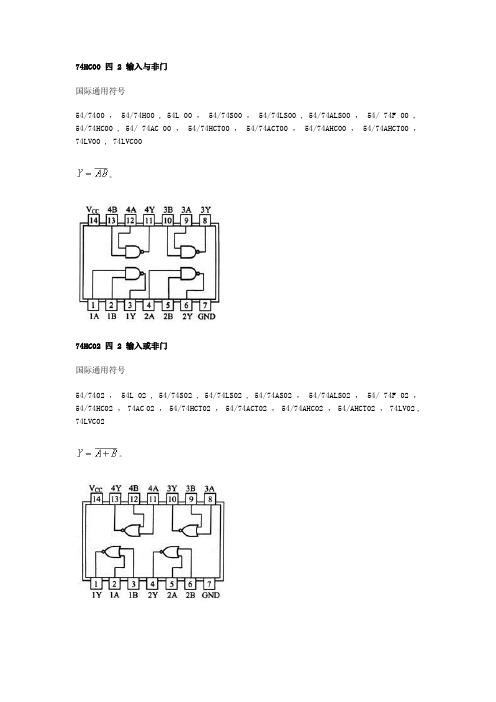
74HC00 四 2 输入与非门国际通用符号54/7400 , 54/74H00 , 54L 00 , 54/74S00 , 54/74LS00 , 54/74ALS00 , 54/ 74F 00 , 54/74HC00 , 54/ 74AC 00 , 54/74HCT00 , 54/74ACT00 , 54/74AHC00 , 54/74AHCT00 ,74LV00 , 74LVC00。
74HC02 四 2 输入或非门国际通用符号54/7402 , 54L 02 , 54/74S02 , 54/74LS02 , 54/74AS02 , 54/74ALS02 , 54/ 74F 02 ,54/74HC02 , 74AC 02 , 54/74HCT02 , 54/74ACT02 , 54/74AHC02 , 54/AHCT02 , 74LV02 , 74LVC02。
74HC04 六反相器国际通用符号54/7404 , 54L 04 , 54/74H04 , 54/74S04 , 54/74LS04 , 54/74AS04 , 54/74ALS04 ,54/ 74F 04 , 54/74HCU04 , 54/74HC04 , 54/ 74AC 04 , 54/74HCT04 , 54/74ACT04 ,54/74AHC04 , 54/74AHCT04 , 74LV04 , 74LVC04 , 54/74AHCU04 , 74LVU04 , 74LVCU04 .74HC08 四 2 输入与门国际通用符号54/7408 , 54/74S08 , 54/74LS08 , 54/74AS08 , 54/74ALS08 , 54/ 74F 08 , 54/74HC08 ,54/74HCT08 , 54/ 74AC 08 , 54/74ACT08 , 54/74AHC08 , 54/74AHCT08 , 74LV08 , 74LVC08。
TTL,CMOS型号内容---------------------------------------------------- 74ls00 2输入四与非门74ls01 2输入四与非门 (oc)74ls02 2输入四或非门74ls03 2输入四与非门 (oc)74ls04 六倒相器74ls05 六倒相器(oc)74ls06 六高压输出反相缓冲器/驱动器(oc,30v)74ls07 六高压输出缓冲器/驱动器(oc,30v)74ls08 2输入四与门74ls09 2输入四与门(oc)74ls10 3输入三与非门74ls11 3输入三与门74ls12 3输入三与非门 (oc)74ls13 4输入双与非门 (斯密特触发)74ls14 六倒相器(斯密特触发)74ls15 3输入三与门 (oc)74ls16 六高压输出反相缓冲器/驱动器(oc,15v)74ls17 六高压输出缓冲器/驱动器(oc,15v)74ls18 4输入双与非门 (斯密特触发)74ls19 六倒相器(斯密特触发)74ls20 4输入双与非门74ls21 4输入双与门74ls22 4输入双与非门(oc)74ls23 双可扩展的输入或非门74ls24 2输入四与非门(斯密特触发)74ls25 4输入双或非门(有选通)74ls26 2输入四高电平接口与非缓冲器(oc,15v)74ls27 3输入三或非门74ls28 2输入四或非缓冲器74ls30 8输入与非门74ls31 延迟电路74ls32 2输入四或门74ls33 2输入四或非缓冲器(集电极开路输出)74ls34 六缓冲器74ls35 六缓冲器(oc)74ls36 2输入四或非门(有选通)74ls37 2输入四与非缓冲器74ls38 2输入四或非缓冲器(集电极开路输出)74ls39 2输入四或非缓冲器(集电极开路输出)74ls40 4输入双与非缓冲器74ls41 bcd-十进制计数器74ls42 4线-10线译码器(bcd输入)74ls43 4线-10线译码器(余3码输入)74ls44 4线-10线译码器(余3葛莱码输入)74ls45 bcd-十进制译码器/驱动器74ls46 bcd-七段译码器/驱动器74ls47 bcd-七段译码器/驱动器74ls48 bcd-七段译码器/驱动器74ls49 bcd-七段译码器/驱动器(oc)74ls50 双二路2-2输入与或非门(一门可扩展)74ls51 双二路2-2输入与或非门74ls51 二路3-3输入,二路2-2输入与或非门74ls52 四路2-3-2-2输入与或门(可扩展)74ls53 四路2-2-2-2输入与或非门(可扩展)74ls53 四路2-2-3-2输入与或非门(可扩展)74ls54 四路2-2-2-2输入与或非门74ls54 四路2-3-3-2输入与或非门74ls54 四路2-2-3-2输入与或非门74ls55 二路4-4输入与或非门(可扩展)74ls60 双四输入与扩展74ls61 三3输入与扩展74ls62 四路2-3-3-2输入与或扩展器74ls63 六电流读出接口门74ls64 四路4-2-3-2输入与或非门74ls65 四路4-2-3-2输入与或非门(oc)74ls70 与门输入上升沿jk触发器74ls71 与输入r-s主从触发器74ls72 与门输入主从jk触发器74ls73 双j-k触发器(带清除端)74ls74 正沿触发双d型触发器(带预置端和清除端)74ls75 4位双稳锁存器74ls76 双j-k触发器(带预置端和清除端)74ls77 4位双稳态锁存器74ls78 双j-k触发器(带预置端,公共清除端和公共时钟端) 74ls80 门控全加器74ls81 16位随机存取存储器74ls82 2位二进制全加器(快速进位)74ls83 4位二进制全加器(快速进位)74ls84 16位随机存取存储器74ls85 4位数字比较器74ls86 2输入四异或门74ls87 四位二进制原码/反码/oi单元74ls89 64位读/写存储器74ls90 十进制计数器74ls91 八位移位寄存器74ls92 12分频计数器(2分频和6分频)74ls93 4位二进制计数器74ls94 4位移位寄存器(异步)74ls95 4位移位寄存器(并行io)74ls96 5位移位寄存器74ls97 六位同步二进制比率乘法器74ls100 八位双稳锁存器74ls103 负沿触发双j-k主从触发器(带清除端)74ls106 负沿触发双j-k主从触发器(带预置,清除,时钟) 74ls107 双j-k主从触发器(带清除端)74ls108 双j-k主从触发器(带预置,清除,时钟)74ls109 双j-k触发器(带置位,清除,正触发)74ls110 与门输入j-k主从触发器(带锁定)74ls111 双j-k主从触发器(带数据锁定)74ls112 负沿触发双j-k触发器(带预置端和清除端)74ls113 负沿触发双j-k触发器(带预置端)74ls114 双j-k触发器(带预置端,共清除端和时钟端)74ls116 双四位锁存器74ls120 双脉冲同步器/驱动器74ls121 单稳态触发器(施密特触发)74ls122 可再触发单稳态多谐振荡器(带清除端)74ls123 可再触发双单稳多谐振荡器74ls125 四总线缓冲门(三态输出)74ls126 四总线缓冲门(三态输出)74ls128 2输入四或非线驱动器74ls131 3-8译码器74ls132 2输入四与非门(斯密特触发)74ls133 13输入端与非门74ls134 12输入端与门(三态输出)74ls135 四异或/异或非门74ls136 2输入四异或门(oc)74ls137 八选1锁存译码器/多路转换器74ls138 3-8线译码器/多路转换器74ls139 双2-4线译码器/多路转换器74ls140 双4输入与非线驱动器74ls141 bcd-十进制译码器/驱动器74ls142 计数器/锁存器/译码器/驱动器74ls145 4-10译码器/驱动器74ls147 10线-4线优先编码器74ls148 8线-3线八进制优先编码器74ls150 16选1数据选择器(反补输出)74ls151 8选1数据选择器(互补输出)74ls152 8选1数据选择器多路开关74ls153 双4选1数据选择器/多路选择器74ls154 4线-16线译码器74ls155 双2-4译码器/分配器(图腾柱输出)74ls156 双2-4译码器/分配器(集电极开路输出)74ls157 四2选1数据选择器/多路选择器74ls158 四2选1数据选择器(反相输出)74ls160 可预置bcd计数器(异步清除)74ls161 可预置四位二进制计数器(并清除异步)74ls162 可预置bcd计数器(异步清除)74ls163 可预置四位二进制计数器(并清除异步)74ls164 8位并行输出串行移位寄存器74ls165 并行输入8位移位寄存器(补码输出)74ls166 8位移位寄存器74ls167 同步十进制比率乘法器(录入编辑:电路图网dzdlt) 74ls168 4位加/减同步计数器(十进制)74ls169 同步二进制可逆计数器74ls170 4*4寄存器堆74ls171 四d触发器(带清除端)74ls172 16位寄存器堆74ls173 4位d型寄存器(带清除端)74ls174 六d触发器74ls175 四d触发器74ls176 十进制可预置计数器74ls177 2-8-16进制可预置计数器74ls178 四位通用移位寄存器74ls179 四位通用移位寄存器74ls180 九位奇偶产生/校验器74ls181 算术逻辑单元/功能发生器74ls182 先行进位发生器74ls183 双保留进位全加器74ls184 bcd-二进制转换器74ls185 二进制-bcd转换器74ls190 同步可逆计数器(bcd,二进制)74ls191 同步可逆计数器(bcd,二进制)74ls192 同步可逆计数器(bcd,二进制)74ls193 同步可逆计数器(bcd,二进制)74ls194 四位双向通用移位寄存器74ls195 四位通用移位寄存器74ls196 可预置计数器/锁存器74ls197 可预置计数器/锁存器(二进制)74ls198 八位双向移位寄存器74ls199 八位移位寄存器74ls210 2-5-10进制计数器74ls213 2-n-10可变进制计数器74ls221 双单稳触发器74ls230 八3态总线驱动器74ls231 八3态总线反向驱动器74ls240 八缓冲器/线驱动器/线接收器(反码三态输出) 74ls241 八缓冲器/线驱动器/线接收器(原码三态输出) 74ls242 八缓冲器/线驱动器/线接收器74ls243 4同相三态总线收发器74ls244 八缓冲器/线驱动器/线接收器74ls245 八双向总线收发器74ls246 4线-七段译码/驱动器(30v)74ls247 4线-七段译码/驱动器(15v)74ls248 4线-七段译码/驱动器74ls249 4线-七段译码/驱动器74ls251 8选1数据选择器(三态输出)74ls253 双四选1数据选择器(三态输出)74ls256 双四位可寻址锁存器74ls257 四2选1数据选择器(三态输出)74ls258 四2选1数据选择器(反码三态输出)74ls259 8为可寻址锁存器74ls260 双5输入或非门74ls261 4*2并行二进制乘法器74ls265 四互补输出元件74ls266 2输入四异或非门(oc)74ls270 2048位rom (512位四字节,oc)74ls271 2048位rom (256位八字节,oc)74ls273 八d触发器74ls274 4*4并行二进制乘法器74ls275 七位片式华莱士树乘法器74ls276 四jk触发器74ls278 四位可级联优先寄存器74ls279 四s-r锁存器74ls280 9位奇数/偶数奇偶发生器/较验器74ls28174ls283 4位二进制全加器74ls290 十进制计数器74ls291 32位可编程模74ls293 4位二进制计数器74ls294 16位可编程模74ls295 四位双向通用移位寄存器74ls298 四-2输入多路转换器(带选通)74ls299 八位通用移位寄存器(三态输出)74ls348 8-3线优先编码器(三态输出)74ls352 双四选1数据选择器/多路转换器74ls353 双4-1线数据选择器(三态输出)74ls354 8输入端多路转换器/数据选择器/寄存器,三态补码输出74ls355 8输入端多路转换器/数据选择器/寄存器,三态补码输出74ls356 8输入端多路转换器/数据选择器/寄存器,三态补码输出74ls357 8输入端多路转换器/数据选择器/寄存器,三态补码输出74ls365 6总线驱动器74ls366 六反向三态缓冲器/线驱动器74ls367 六同向三态缓冲器/线驱动器74ls368 六反向三态缓冲器/线驱动器74ls373 八d锁存器74ls374 八d触发器(三态同相)74ls375 4位双稳态锁存器74ls377 带使能的八d触发器74ls378 六d触发器74ls379 四d触发器74ls381 算术逻辑单元/函数发生器74ls382 算术逻辑单元/函数发生器74ls384 8位*1位补码乘法器74ls385 四串行加法器/乘法器74ls386 2输入四异或门74ls390 双十进制计数器74ls391 双四位二进制计数器74ls395 4位通用移位寄存器74ls396 八位存储寄存器74ls398 四2输入端多路开关(双路输出)74ls399 四-2输入多路转换器(带选通)74ls422 单稳态触发器74ls423 双单稳态触发器74ls440 四3方向总线收发器,集电极开路74ls441 四3方向总线收发器,集电极开路74ls442 四3方向总线收发器,三态输出74ls443 四3方向总线收发器,三态输出74ls444 四3方向总线收发器,三态输出74ls445 bcd-十进制译码器/驱动器,三态输出74ls446 有方向控制的双总线收发器74ls448 四3方向总线收发器,三态输出74ls449 有方向控制的双总线收发器74ls465 八三态线缓冲器74ls466 八三态线反向缓冲器74ls467 八三态线缓冲器74ls468 八三态线反向缓冲器74ls490 双十进制计数器74ls540 八位三态总线缓冲器(反向)74ls541 八位三态总线缓冲器74ls589 有输入锁存的并入串出移位寄存器74ls590 带输出寄存器的8位二进制计数器74ls591 带输出寄存器的8位二进制计数器74ls592 带输出寄存器的8位二进制计数器74ls593 带输出寄存器的8位二进制计数器74ls594 带输出锁存的8位串入并出移位寄存器74ls595 8位输出锁存移位寄存器74ls596 带输出锁存的8位串入并出移位寄存器74ls597 8位输出锁存移位寄存器74ls598 带输入锁存的并入串出移位寄存器74ls599 带输出锁存的8位串入并出移位寄存器74ls604 双8位锁存器74ls605 双8位锁存器74ls606 双8位锁存器74ls607 双8位锁存器74ls620 8位三态总线发送接收器(反相)74ls621 8位总线收发器74ls622 8位总线收发器74ls623 8位总线收发器74ls640 反相总线收发器(三态输出)74ls641 同相8总线收发器,集电极开路74ls642 同相8总线收发器,集电极开路74ls643 8位三态总线发送接收器74ls644 真值反相8总线收发器,集电极开路74ls645 三态同相8总线收发器74ls646 八位总线收发器,寄存器74ls647 八位总线收发器,寄存器74ls648 八位总线收发器,寄存器74ls649 八位总线收发器,寄存器74ls651 三态反相8总线收发器(录入编辑:电路图网dzdlt) 74ls652 三态反相8总线收发器74ls653 反相8总线收发器,集电极开路74ls654 同相8总线收发器,集电极开路74ls668 4位同步加/减十进制计数器74ls669 带先行进位的4位同步二进制可逆计数器74ls670 4*4寄存器堆(三态)74ls671 带输出寄存的四位并入并出移位寄存器74ls672 带输出寄存的四位并入并出移位寄存器74ls673 16位并行输出存储器,16位串入串出移位寄存器74ls674 16位并行输入串行输出移位寄存器74ls681 4位并行二进制累加器74ls682 8位数值比较器(图腾柱输出)74ls683 8位数值比较器(集电极开路)74ls684 8位数值比较器(图腾柱输出)74ls685 8位数值比较器(集电极开路)74ls686 8位数值比较器(图腾柱输出)74ls687 8位数值比较器(集电极开路)74ls688 8位数字比较器(oc输出)74ls689 8位数字比较器74ls690 同步十进制计数器/寄存器(带数选,三态输出,直接清除)74ls691 计数器/寄存器(带多转换,三态输出)74ls692 同步十进制计数器(带预置输入,同步清除)74ls693 计数器/寄存器(带多转换,三态输出)74ls696 同步加/减十进制计数器/寄存器(带数选,三态输出,直接清除) 74ls697 计数器/寄存器(带多转换,三态输出)74ls698 计数器/寄存器(带多转换,三态输出)74ls699 计数器/寄存器(带多转换,三态输出)74ls716 可编程模n十进制计数器74ls718 可编程模n十进制计数器CD4001 4二输入或非门CD4002 双4输入或非门CD4006 18位静态移位寄存器CD4007 双互补对加反相器CD4009 六缓冲器/转换-倒相CD4010 六缓冲器/转换-正相CD4011 四2输入与非门CD4012 双4输入与非门CD4013 置/复位双D型触发器CD4014 8位静态同步移位寄存CD4015 双4位静态移位寄存器CD4016 四双向模拟数字开关CD4017 10译码输出十进制计数器CD4018 可预置1/N计数器CD4019 四与或选择门CD4020 14位二进制计数器CD4021 8位静态移位寄存器CD4022 8译码输出8进制计数器CD4023 三3输入与非门CD4024 7位二进制脉冲计数器CD4025 三3输入与非门CD4026 十进制/7段译码/驱动CD4027 置位/复位主从触发器CD4028 BCD十进制译码器CD4029 4位可预置可逆计数器CD4030 四异或门CD4031 64位静态移位寄存器CD4032 三串行加法器CD4033 十进制计数器/7段显示CD4034 8位静态移位寄存器CD4035 4位并入/并出移位寄存器CD4038 3位串行加法器CD4040 12位二进制计数器CD4041 四原码/补码缓冲器CD4042 四时钟D型锁存器CD4043 四或非R/S锁存器CD4044 四与非R/S锁存器CD4046 锁相环CD4047 单非稳态多谐振荡器CD4048 可扩充八输入门CD4049 六反相缓冲/转换器CD4050 六正相缓冲/转换器CD4051 单8通道多路转换/分配CD4052 双4通道多路转换/分配CD4053 三2通道多路转换/分配CD4056 7段液晶显示译码/驱动CD4060 二进制计数/分频/振荡CD4063 四位数值比较器CD4066 四双相模拟开管CD4067 16选1模拟开关CD4068 8输入端与非/与门CD4069 六反相器CD4070 四异或门CD4071 四2输入或门CD4072 双四输入或门CD4073 三3输入与门CD4075 三3输入与门CD4076 4位D型寄存器CD4077 四异或非门CD4078 八输入或/或非门CD4081 四输入与门CD4082 双4输入与门CD4085 双2组2输入与或非门CD4086 可扩展2输入与或非门CD4093 四与非斯密特触发器CD4094 8位移位/贮存总线寄存CD4096 3输入J-K触发器CD4098 双单稳态触发器CD4099 8位可寻址锁存器CD40103 同步可预置减法器CD40106 六斯密特触发器CD40107 双2输入与非缓冲/驱动CD40110 计数/译码/锁存/驱动CD40174 6D触发器CD40175 4D触发器CD40192 BCD可预置可逆计数器CD40193 二进制可预置可逆计数器CD40194 4位双相移位寄存器。


CC4067------16选1模拟开关简要说明:CC4067 是数字控制模拟开关,具有低导通阻抗,低截止漏电流和内部地址译码的特征。
另外,在整个输入信号范围内,导通电阻保持相对稳定。
CC4067是16通道开关,有四个二进制输入端A0~A3和控制端C,输入的任意一个组合可选择一路开关。
C=1时,关闭所有的通道。
CC4067提供了24引线多层陶瓷双列直插(D)、熔封陶瓷双列直插(J)、塑料双列直插(P)和陶瓷片状载体(C)4种封装形式。
推荐工作条件:电源电压范围…………3V~15V输入电压范围…………0V~V DD工作温度范围M类…………-55℃~125℃E类………….-40℃~85℃极限值:电源电压…...-0.5V~18V输入电压……-0.5V~V DD+0.5V输入电流…………….±10mA储存温度…………-65℃~150℃引出端符号:A0~A3 地址端C 控制端I0/O0~I15/O15输入/输出通道O/I 公共输出/输入端V DD正电源Vss 地逻辑符号:引出端排列(俯视):逻辑表达式:I I 输入电流(最大)V IN =18V/0V 18 ±0.1±0.1µA t R =t F =20nS;C L =50pFR L =10k Ω t PLHt PHL 传输延迟时间(导通)(最大)A->O/I C->O/I-0 0 0 5.0 10.015.0-650 270 190 nSt R =t F =20nS;C L =50pFRL=300Ωt PLHt PHL 传输延迟时间(截止) (最大)A->O /I C->O/I -0 0 0 5.0 10.015.0-440 180 130 nS控制部分(A0、A1、A2、A3、C) C I 输入电容(最大) A 、C -- 7.5pF* 峰-峰电压对称值为(V DD-V EE)/2 ** 最坏情况** 两通道的末端逻辑图:。


74HC4067; 74HCT406716-channel analog multiplexer/demultiplexerRev. 03 — 15 October 2007Product data sheet1.General descriptionThe74HC4067;74HCT4067is a high-speed Si-gate CMOS device and is pin compatiblewith the HEF4067B. The device is specified in compliance with JEDEC standard no. 7A.The 74HC4067; 74HCT4067 is a 16-channel analog multiplexer/demultiplexer with fouraddress inputs (S0 to S3), an active-LOW enable input (E), sixteen independentinputs/outputs (Y0 to Y15) and a common input/output (Z).The 74HC4067; 74HCT4067 contains sixteen bidirectional analog switches, each withone side connected to an independent input/output (Y0 to Y15) and the other sideconnected to a common input/output (Z).With pin E = LOW, one of the sixteen switches is selected by pins S0 to S3 (lowimpedance ON-state). All unselected switches are in the high-impedance OFF-state.With pin E=HIGH,all switches are in the high-impedance OFF-state,independent of pinsS0 to S3.The analog inputs/outputs (Y0 to Y15, and Z) can swing between V CC as a positive limitand GND as a negative limit. V CC to GND may not exceed 10V.2.FeaturesI Low ON resistance:N80Ω (typical) at V CC = 4.5VN70Ω (typical) at V CC = 6.0VN60Ω (typical) at V CC = 9.0VI Typical ‘break before make’ built-in3.ApplicationsI Analog multiplexing and demultiplexingI Digital multiplexing and demultiplexingI Signal gating4.Ordering informationTable 1.Ordering informationType number PackageTemperature range Name Description Version 74HC406774HC4067N−40°C to +125°C DIP24plastic dual in-line package; 24leads (600mil);SOT101-1reverse bendingSOT137-1 74HC4067D−40°C to +125°C SO24plastic small outline package; 24leads;body width7.5mm74HC4067DB−40°C to +125°C SSOP24plastic shrink small outline package; 24leads;SOT340-1body width5.3mmSOT355-1 74HC4067PW−40°C to +125°C TSSOP24plastic thin shrink small outline package; 24leads;body width4.4mmSOT815-1 74HC4067BQ−40°C to +125°C DHVQFN24plastic dual in-line compatible thermal enhanced verythin quad flat package; no leads; 24terminals;body3.5×5.5×0.85mm74HCT4067SOT101-1 74HCT4067N−40°C to +125°C DIP24plastic dual in-line package; 24leads (600mil);reverse bendingSOT137-1 74HCT4067D−40°C to +125°C SO24plastic small outline package; 24leads;body width7.5mmSOT340-1 74HCT4067DB−40°C to +125°C SSOP24plastic shrink small outline package; 24leads;body width5.3mmSOT355-1 74HCT4067PW−40°C to +125°C TSSOP24plastic thin shrink small outline package; 24leads;body width4.4mmSOT815-1 74HCT4067BQ−40°C to +125°C DHVQFN24plastic dual in-line compatible thermal enhanced verythin quad flat package; no leads; 24terminals;body3.5×5.5×0.85mm5.Functional diagramFig 1.Logic symbol Fig 2.IEC logic symbol001aag7259Y0810Y1S011S114S213S315E7Y26Y35Y44Y5Z13Y62Y723Y822Y921Y1020Y1119Y1218Y1317Y1416Y15MUX/DMUX39G168761543201234567232221201918171689101112131415001aag72616 ×0151011141315Fig 3.Schematic diagram (one switch)001aag729YnZGNDfrom logicV CC V CCFig 4.Functional diagram001aag7271-OF-16DECODER109Y0S08Y17Y26Y35Y44Y53Y62Y723Y822Y921Y1020Y1119Y1218Y1317Y1416Y151Z11S114S213S315EY0Y1Y2Y3Y4 S0Y5Y6Y7 S1Y8Y9Y10 S2Y11Y12Y13 S3Y14Y15 EZ001aag728Fig 5.Logic diagram6.Pinning information6.1Pinning6.2Pin description(1)The die substrate is attached to this pad usingconductive die attach material.It can not be used as supply pin or input.Fig 6.Pin configuration for DIP24,SO24,SSOP24andTSSOP24Fig 7.Pin configuration for DHVQFN2474HC406774HCT4067Z V CC Y7Y8Y6Y9Y5Y10Y4Y11Y3Y12Y2Y13Y1Y14Y0Y15S0E S1S2GND S3001aag730123456789101112141316151817201922212423001aag73174HC406774HCT4067Transparent top viewS2S0S1E Y0Y15Y1Y14Y2Y13Y3Y12Y4Y11Y5Y10Y6Y9Y7Y8G N D S 3ZV C C111410159168177186195204213222231213124terminal 1index areaV CC (1)Table 2.Pin description Symbol Pin Description Z 1common input/output Y72independent input/output 7Y63independent input/output 6Y54independent input/output 5Y45independent input/output 4Y36independent input/output 3Y27independent input/output 2Y18independent input/output 1Y09independent input/output 0S010address input 0S111address input 1GND 12ground (0V)S313address input 3S214address input 2Table 2.Pin description …continuedSymbol Pin DescriptionE15enable input (active LOW)Y1516independent input/output 15Y1417independent input/output 14Y1318independent input/output 13Y1219independent input/output 12Y1120independent input/output 11Y1021independent input/output 10Y922independent input/output 9Y823independent input/output 8V CC24supply voltage7.Functional descriptionTable 3.Function table[1]Inputs Channel ON E S3S2S1S0L L L L L Y0to ZL L L L H Y1to ZL L L H L Y2to ZL L L H H Y3 to ZL L H L L Y4 to ZL L H L H Y5 to ZL L H H L Y6 to ZL L H H H Y7 to ZL H L L L Y8 to ZL H L L H Y9 to ZL H L H L Y10 to ZL H L H H Y11 to ZL H H L L Y12 to ZL H H L H Y13 to ZL H H H L Y14 to ZL H H H H Y15 to ZH X X X X-[1]H = HIGH voltage level;L = LOW voltage level;X = don’t care.8.Limiting valuesTable 4.Limiting valuesIn accordance with the Absolute Maximum Rating System (IEC 60134). Voltages are referenced to GND (ground = 0V). Symbol Parameter Conditions Min Max UnitV CC supply voltage[1]−0.5+11.0VI IK input clamping current V I<−0.5V or V I>V CC+0.5V-±20mAI SK switch clamping current V SW<−0.5V or V SW>V CC+0.5V-±20mAI SW switch current V SW=−0.5V to (V CC+0.5V)-±25mAI CC supply current-50mAI GND ground current-−50mAT stg storage temperature−65+150°CP tot total power dissipation T amb =−40°C to +125°CDIP24 package[2]-750mWSO24 package[3]-500mWSSOP24 package[4]-500mWTSSOP24 package[4]-500mWDHVQFN24 package[5]-500mWP power dissipation per switch-100mW [1]To avoid drawing V CC current out of terminal Z, when switch current flows in terminals Yn, the voltage drop across the bidirectionalswitch must not exceed0.4V.If the switch currentflows into terminal Z,no V CC current willflow out of terminals Yn.In this case there is no limit for the voltage drop across the switch, but the voltages at Yn and Z may not exceed V CC or GND.[2]For DIP24 package: P tot derates linearly with 12mW/K above 70°C.[3]For SO24 package: P tot derates linearly with 8mW/K above 70°C.[4]For SSOP24 and TSSOP24 packages: P tot derates linearly with 5.5mW/K above 60°C.[5]For DHVQFN24 package: P tot derates linearly with 4.5mW/K above 60°C.9.Recommended operating conditionsTable 5.Recommended operating conditionsSymbol Parameter Conditions Min Typ Max Unit74HC4067V CC supply voltage 2.0 5.010.0VV I input voltage GND-V CC VV SW switch voltage GND-V CC Vt r rise time V CC = 2.0V--1000nsV CC = 4.5V- 6.0500nsV CC = 6.0V--400nsV CC = 10.0V--250nst f fall time V CC = 2.0V--1000nsV CC = 4.5V- 6.0500nsV CC = 6.0V--400nsV CC = 10.0V--250nsT amb ambient temperature−40+25+125°C10.Static characteristics[1]At supply voltages (V CC − GND) approaching 2V , the analog switch ON resistance becomes extremely non-linear. Therefore it is recommended that these devices be used to transmit digital signals only, when using these supply voltages.74HCT4067V CC supply voltage 4.5 5.0 5.5V V I input voltage GND -V CC V V SW switch voltage GND -V CC V t r rise time V CC = 4.5V - 6.0500ns t f fall timeV CC = 4.5V - 6.0500ns T ambambient temperature−40+25+125°CTable 5.Recommended operating conditions …continued Symbol Parameter ConditionsMin Typ Max Unit Table 6.R ON resistance per switch for types 74HC4067 and 74HCT4067V I = V IH or V IL ; for test circuit see Figure 8.V is is the input voltage at a Yn or Z terminal, whichever is assigned as an input.V os is the output voltage at a Yn or Z terminal, whichever is assigned as an output.For 74HC4067: V CC − GND = 2.0V , 4.5V , 6.0V and 9.0V .For 74HCT4067: V CC − GND = 4.5V .SymbolParameterConditions25°C−40°C to +125°C Unit TypMaxMax (85°C)Max(125°C)R ON(peak)ON resistance (peak)V is = V CC to GNDV CC = 2.0V; I SW = 100µA [1]----ΩV CC = 4.5V; I SW = 1000µA 110180225270ΩV CC = 6.0V; I SW = 1000µA 95160200240ΩV CC = 9.0V; I SW = 1000µA75130165195ΩR ON(rail)ON resistance (rail)V is = GND or V CCV CC = 2.0V; I SW = 100µA [1]150---V CC = 4.5V; I SW = 1000µA 90160200240ΩV CC = 6.0V; I SW = 1000µA 80140175210ΩV CC = 9.0V; I SW = 1000µA70120150180Ω∆R ONON resistance mismatch between channels V is = V CC to GND V CC = 2.0V[1]----ΩV CC = 4.5V 9---ΩV CC = 6.0V 8---ΩV CC = 9.0V6---ΩV is = 0V to (V CC − GND)V is = 0V to (V CC − GND)(1)V CC = 4.5V (2)V CC = 6.0V (3)V CC = 9.0VFig 8.Test circuit for measuring R ON Fig 9.Typical R ON as a function of input voltage V is001aag733V ILZV CCYnE I SWV isGNDV SW V is (V)09.07.23.6 5.41.8mnb0475070309011010R ON (Ω)(1)(2)(3)R ONV SW I SW----------=Table 7.Static characteristics 74HC4067At recommended operating conditions; voltages are referenced to GND (ground = 0V).V is is the input voltage at a Yn or Z terminal, whichever is assigned as an input.V os is the output voltage at a Yn or Z terminal, whichever is assigned as an output.Symbol ParameterConditions Min Typ Max Unit T amb = 25°CV IHHIGH-level input voltageV CC = 2.0V 1.5 1.2-V V CC = 4.5V 3.15 2.4-V V CC = 6.0V 4.2 3.2-V V CC = 9.0V6.3 4.7-V V ILLOW-level input voltageV CC = 2.0V -0.80.5V V CC = 4.5V - 2.1 1.35V V CC = 6.0V - 2.8 1.80V V CC = 9.0V- 4.32.70VI Iinput leakage currentV I = V CC or GND V CC = 6.0V --±0.1µA V CC = 10.0V--±0.2µAI S(OFF)OFF-state leakage currentV CC = 10.0V; V I = V IH or V IL ;|V SW |=V CC −GND ; see Figure 10per channel --±0.1µA all channels--±0.8µA I S(ON)ON-state leakage currentV CC = 10.0V; V I = V IH or V IL ;|V SW |=V CC −GND ; see Figure 11--±0.8µAI CCsupply currentV I =V CC or GND;V is =GND or V CC ;V os =V CC or GND V CC = 6.0V --8.0µA V CC = 10.0V--16.0µA C I input capacitance - 3.5-pFT amb =−40°C to +85°CV IHHIGH-level input voltageV CC = 2.0V 1.5--V V CC = 4.5V 3.15--V V CC = 6.0V 4.2--V V CC = 9.0V6.3--V V ILLOW-level input voltageV CC = 2.0V --0.50V V CC = 4.5V -- 1.35V V CC = 6.0V -- 1.80V V CC = 9.0V-- 2.70VI Iinput leakage currentV I = V CC or GND V CC = 6.0V --±1.0µA V CC = 10.0V--±2.0µAI S(OFF)OFF-state leakage currentV CC = 10.0V; V I = V IH or V IL ;|V SW |=V CC −GND ; see Figure 10per channel --±1.0µA all channels--±8.0µA I S(ON)ON-state leakage current V CC = 10.0V; V I = V IH or V IL ;|V SW |=V CC −GND ; see Figure 11--±8.0µAI CCsupply currentV I =V CC or GND;V is =GND or V CC ;V os =V CC or GND V CC = 6.0V --80.0µA V CC = 10.0V--160µAT amb =−40°C to +125°C V IHHIGH-level input voltageV CC = 2.0V 1.5--V V CC = 4.5V 3.15--V V CC = 6.0V 4.2--V V CC = 9.0V6.3--V V ILLOW-level input voltageV CC = 2.0V --0.50V V CC = 4.5V -- 1.35V V CC = 6.0V -- 1.80V V CC = 9.0V-- 2.70VI Iinput leakage currentV I = V CC or GND V CC = 6.0V --±1.0µA V CC = 10.0V--±2.0µATable 7.Static characteristics 74HC4067 …continuedAt recommended operating conditions; voltages are referenced to GND (ground = 0V).V is is the input voltage at a Yn or Z terminal, whichever is assigned as an input.V os is the output voltage at a Yn or Z terminal, whichever is assigned as an output.Symbol Parameter ConditionsMinTypMaxUnitI S(OFF)OFF-state leakage currentV CC = 10.0V; V I = V IH or V IL ;|V SW |=V CC −GND ; see Figure 10per channel --±1.0µA all channels--±8.0µA I S(ON)ON-state leakage current V CC = 10.0V; V I = V IH or V IL ;|V SW |=V CC −GND ; see Figure 11--±8.0µAI CCsupply currentV I =V CC or GND;V is =GND or V CC ;V os =V CC or GND V CC = 6.0V --160µA V CC = 10.0V--320µATable 7.Static characteristics 74HC4067 …continuedAt recommended operating conditions; voltages are referenced to GND (ground = 0V).V is is the input voltage at a Yn or Z terminal, whichever is assigned as an input.V os is the output voltage at a Yn or Z terminal, whichever is assigned as an output.Symbol ParameterConditionsMinTypMaxUnitTable 8.Static characteristics 74HCT4067At recommended operating conditions; voltages are referenced to GND (ground = 0V).V is is the input voltage at a Yn or Z terminal, whichever is assigned as an input.V os is the output voltage at a Yn or Z terminal, whichever is assigned as an output.Symbol ParameterConditions Min Typ Max Unit T amb = 25°CV IH HIGH-level input voltage V CC = 4.5V to 5.5V 2.0 1.6-V V IL LOW-level input voltage V CC = 4.5V to 5.5V- 1.20.8V I I input leakage current V I = V CC or GND; V CC = 5.5V --±0.1µAI S(OFF)OFF-state leakage currentV CC = 5.5V; V I = V IH or V IL ;|V SW |=V CC −GND ; see Figure 10per channel --±0.1µA all channels--±0.8µA I S(ON)ON-state leakage current V CC = 5.5V; V I = V IH or V IL ;|V SW |=V CC −GND ; see Figure 11--±0.8µA I CC supply currentV I = V CC or GND; V is = GND or V CC ;V os =V CC or GND; V CC = 4.5V to 5.5V --8.0µA∆I CCadditional supply currentper input pin;V I =V CC −2.1V;other inputs at V CC or GND; V CC = 4.5V to 5.5V pin E -60216µA pin Sn-50180µA C I input capacitance - 3.5-pFT amb =−40°C to +85°CV IH HIGH-level input voltage V CC = 4.5V to 5.5V 2.0--V V IL LOW-level input voltage V CC = 4.5V to 5.5V--0.8V I I input leakage current V I = V CC or GND; V CC = 5.5V --±1.0µAI S(OFF)OFF-state leakage currentV CC = 5.5V; V I = V IH or V IL ;|V SW |=V CC −GND ; see Figure 10per channel --±1.0µA all channels--±8.0µAI S(ON)ON-state leakage current V CC = 5.5V; V I = V IH or V IL ;|V SW |=V CC −GND ; see Figure 11--±8.0µA I CC supply currentV I = V CC or GND; V is = GND or V CC ;V os =V CC or GND; V CC = 4.5V to 5.5V --80.0µA∆I CCadditional supply currentper input pin; V I = V CC − 2.1V; otherinputs at V CC or GND;V CC =4.5V to 5.5V pin E --270µA pin Sn--225µAT amb =−40°C to +125°C V IH HIGH-level input voltage V CC = 4.5V to 5.5V 2.0--V V IL LOW-level input voltage V CC = 4.5V to 5.5V--0.8V I I input leakage current V I = V CC or GND; V CC = 5.5V --±1.0µAI S(OFF)OFF-state leakage currentV CC = 5.5V; V I = V IH or V IL ;|V SW |=V CC −GND ; see Figure 10per channel --±1.0µA all channels--±8.0µA I S(ON)ON-state leakage current V CC = 5.5V; V I = V IH or V IL ;|V SW |=V CC −GND ; see Figure 11--±8.0µA I CC supply currentV I = V CC or GND; V is = GND or V CC ;V os =V CC or GND; V CC = 4.5V to 5.5V --160µA∆I CCadditional supply currentper input pin; V I = V CC − 2.1V; otherinputs at V CC or GND;V CC =4.5V to 5.5V pin E --294µA pin Sn--245µATable 8.Static characteristics 74HCT4067 …continuedAt recommended operating conditions; voltages are referenced to GND (ground = 0V).V is is the input voltage at a Yn or Z terminal, whichever is assigned as an input.V os is the output voltage at a Yn or Z terminal, whichever is assigned as an output.Symbol ParameterConditionsMin Typ Max Unit V is = V CC and V os = GND V is = GND and V os = V CCV is = V CC and V os = open V is = GND and V os = openFig 10.Test circuit for measuring OFF-state leakagecurrent Fig 11.Test circuit for measuring ON-state leakagecurrentI SWI SW001aag734V IHZV CCYnE V osV isGNDI SW001aag735V ILZYnE V osV isGNDV CC11.Dynamic characteristicsTable 9.Dynamic characteristics 74HC4067GND =0V; t r = t f = 6ns; C L = 50pF unless specified otherwise; for test circuit see Figure14.V is is the input voltage at a Yn or Z terminal, whichever is assigned as an input.V os is the output voltage at a Yn or Z terminal, whichever is assigned as an output.Symbol Parameter Conditions25°C−40°C to +125°C UnitTyp Max Max(85°C)Max (125°C)t pd propagation delay Yn to Z; see Figure12[1][2]V CC = 2.0V257595110nsV CC = 4.5V9151922nsV CC = 6.0V7131619nsV CC = 9.0V591114nsZ to YnV CC = 2.0V18607590nsV CC = 4.5V6121518nsV CC = 6.0V5101315nsV CC = 9.0V481012ns t off turn-off time E to Yn; see Figure13[3]V CC = 2.0V74250315375nsV CC = 4.5V27506375nsV CC = 5.0V; C L = 15pF27---nsV CC = 6.0V22435464nsV CC = 9.0V20384857nsSn to YnV CC = 2.0V83250315375nsV CC = 4.5V30506375nsV CC = 5.0V; C L = 15pF29---nsV CC = 6.0V24435464nsV CC = 9.0V21384857nsE to ZV CC = 2.0V852********nsV CC = 4.5V31556983nsV CC = 6.0V25475971nsV CC = 9.0V24425363nsSn to ZV CC = 2.0V94290365435nsV CC = 4.5V34587387nsV CC = 6.0V27476274nsV CC = 9.0V25455668ns[1]t pd is the same as t PHL and t PLH .[2]Due to higher Z terminal capacitance (16 switches versus 1) the delay figures to the Z terminal are higher than those to the Y terminal.[3]t on is the same as t PHZ and t PLZ .[4]t off is the same as t PZH and t PZL .[5]C PD is used to determine the dynamic power dissipation (P D in µW).P D = C PD × V CC 2×f i +∑{(C L +C sw )×V CC 2×f o } where:f i = input frequency in MHz;f o = output frequency in MHz;∑{(C L +C sw )×V CC 2× f o } = sum of outputs;C L = output load capacitance in pF;C sw = switch capacitance in pF;V CC = supply voltage in V .t onturn-on timeE to Yn; see Figure 13[4]V CC = 2.0V 80275345415ns V CC = 4.5V29556983ns V CC = 5.0V; C L = 15pF 26---ns V CC = 6.0V 23475971ns V CC = 9.0V 17425363ns Sn to Yn V CC = 2.0V 88300375450ns V CC = 4.5V32607590ns V CC = 5.0V; C L = 15pF 29---ns V CC = 6.0V 26516477ns V CC = 9.0V 18455668ns E to Z V CC = 2.0V 852********ns V CC = 4.5V 31556983ns V CC = 6.0V 25475971ns V CC = 9.0V 18425363ns Sn to Z V CC = 2.0V 94300375450ns V CC = 4.5V 34607590ns V CC = 6.0V 27516477ns V CC = 9.0V19455668ns C PDpower dissipation capacitanceper switch; V I = GND to V CC[5]-29--pFTable 9.Dynamic characteristics 74HC4067 …continuedGND =0V; t r = t f = 6ns; C L = 50pF unless specified otherwise; for test circuit see Figure 14.V is is the input voltage at a Yn or Z terminal, whichever is assigned as an input.V os is the output voltage at a Yn or Z terminal, whichever is assigned as an output.Symbol ParameterConditions25°C−40°C to +125°C Unit TypMaxMax (85°C)Max (125°C)[1]t pd is the same as t PHL and t PLH .[2]Due to higher Z terminal capacitance (16 switches versus 1) the delay figures to the Z terminal are higher than those to the Y terminal.[3]t on is the same as t PHZ and t PLZ .[4]t off is the same as t PZH and t PZL .[5]C PD is used to determine the dynamic power dissipation (P D in µW).P D = C PD × V CC 2×f i +∑{(C L +C sw )×V CC 2×f o } where:f i = input frequency in MHz;f o = output frequency in MHz;∑{(C L +C sw )×V CC 2× f o } = sum of outputs;C L = output load capacitance in pF;C sw = switch capacitance in pF;V CC = supply voltage in V .Table 10.Dynamic characteristics 74HCT4067GND =0V; t r = t f = 6ns; C L = 50pF unless specified otherwise; for test circuit see Figure 14.V is is the input voltage at a Yn or Z terminal, whichever is assigned as an input.V os is the output voltage at a Yn or Z terminal, whichever is assigned as an output.Symbol ParameterConditions25°C−40°C to +125°C Unit TypMaxMax (85°C)Max (125°C)t pdpropagation delayYn to Z; see Figure 12[1][2]V CC = 4.5V 9151922ns Z to Yn V CC = 4.5V6121518ns t offturn-off timeE to Yn; see Figure 13[3]V CC = 4.5V26556983ns V CC = 5.0V; C L = 15pF 26---ns Sn to Yn V CC = 4.5V31556983ns V CC = 5.0V; C L = 15pF 30---ns E to Z V CC = 4.5V 30607590ns Sn to Z V CC = 4.5V35607590ns t onturn-on timeE to Yn; see Figure 13[4]V CC = 4.5V32607590ns V CC = 5.0V; C L = 15pF 32---ns Sn to Yn V CC = 4.5V35607590ns V CC = 5.0V; C L = 15pF 33---ns E to Z V CC = 4.5V 38658198ns Sn to Z V CC = 4.5V38658198ns C PDpower dissipation capacitanceper switch; V I = GND to (V CC −1.5V)[5]-29--pF12.WaveformsFig 12.Input (V is ) to output (V os )propagation delays001aad555t PLH t PHL50 %50 %V is inputV os outputMeasurement points are shown in Table 11.Fig 13.Turn-on and turn-off times 001aad556t PLZt PHZswitch OFF switch ONswitch ON V os outputV os outputE, Sn inputsV MV I0 V90 %10 %t PZLt PZH50 %50 %Table 11.Measurement pointsType V I V M 74HC4067V CC 0.5V CC 74HCT40673.0V1.3V[1]For 74HCT4067: maximum input voltage V I = 3.0V .Test data is given in T able 12.Definitions test circuit:R T = Termination resistance should be equal to output impedance Z o of the pulse generator.C L = Load capacitance including jig and probe capacitance.R L = Load resistor.S1 = Test selection switch.Fig 14.Load circuitry for measuring switching times V M V Mt Wt W10 %90 %0 VV IV I negative pulsepositive pulse0 VV MV M 90 %10 %t ft r t rt f 001aag732V CC V CCopenGNDV IV osDUTC LR TR LS1PULSE GENERATORV isTable 12.Test dataTestInput OutputS1 positionControl E Address Sn Switch Yn (Z)t r , t f Switch Z (Yn)V I [1]V I [1]V isC L R L t PHL,t PLH GND GND or V CC GND to V CC 6ns 50pF -open t PHZ , t PZH GND to V CC GND to V CC V CC 6ns 50pF , 15pF 1k ΩGND t PLZ , t PZLGND to V CCGND to V CCGND6ns50pF , 15pF1k ΩV CC13.Additional dynamic characteristics[1]Adjust input voltage V is to 0dBm level (0dBm = 1mW into 600Ω).[2]Adjust input voltage V is to 0dBm level at V os for f i =1MHz (0dBm =1mW into 50Ω).After set-up,f i is increased to obtain a reading of −3dB at V os .Table 13.Additional dynamic characteristicsRecommended conditions and typical values; GND = 0V; T amb = 25°C.V is is the input voltage at a Yn or Z terminal, whichever is assigned as an input.V os is the output voltage at a Yn or Z terminal, whichever is assigned as an output.Symbol Parameter ConditionsMin Typ Max UnitTHDtotal harmonic distortionR L = 10k Ω; C L = 50pF; see Figure 15f i = 1kHzV CC = 4.5V; V is(p-p) = 4.0V -0.04-%V CC = 9.0V; V is(p-p) = 8.0V -0.02-%f i = 10kHzV CC = 4.5V; V is(p-p) = 4.0V -0.12-%V CC = 9.0V; V is(p-p) = 8.0V-0.06-%αisoisolation (OFF-state)R L = 600Ω; C L = 50pF; see Figure 16[1]V CC = 4.5V -−50-dB V CC = 9.0V-−50-dB f (-3dB)−3dB frequency responseR L = 50Ω;C L = 10pF; see Figure 17[2]V CC = 4.5V -90-MHz V CC = 9.0V-100-MHz C swswitch capacitanceindependent pins Y -5-pF common pin Z-45-pFFig 15.Test circuit for measuring total harmonic distortion10 µF 001aag736V ILZGNDYnEV osDV CC2R L2R LC LV is f iV CCa.Isolation (OFF-state)b.T est circuitV CC = 4.5V; GND = 0V; R L = 50Ω; R source = 1k Ω.Fig 16.Isolation (OFF-state) as a function of frequency001aae332f i (kHz)10105106104102103−60−40−80−200αiso (dB)−1000.1 µF 001aag737V IHZGNDYnEV os V CC2R L2R LC LV is f idBV CCa.T ypical −3dB frequency responseb.T est circuitV CC = 4.5V; GND = 0V; R L = 50Ω; R source = 1k Ω.Fig 17.−3dB frequency response001aag739f i (kHz)1010510610410210305V os (dB)−50.1 µF 001aag738V ILZdBYnEV os V CC2R L2R LC LV is f iGNDV CC14.Package outlineFig 18.Package outline SOT101-1 (DIP24)UNIT Amax.12b 1c D E e M H L REFERENCESOUTLINE VERSION EUROPEAN PROJECTIONISSUE DATE IEC JEDEC JEITA mm inchesDIMENSIONS (inch dimensions are derived from the original mm dimensions)SOT101-199-12-2703-02-13A min. A max.b w M E e 11.71.30.530.380.320.2332.031.414.113.7 3.93.40.252.5415.2415.8015.2417.1515.90 2.25.10.5140.0660.0510.0210.0150.0130.0091.261.240.560.540.150.130.010.10.60.620.600.680.630.0870.20.020.16051G02MO-015SC-509-24M Hc(e )1M EALs e a t i n g p l a n eA 1w Mb 1eDA 2Z2411312bEpin 1 index0510 mmscaleNote1. Plastic or metal protrusions of 0.25 mm (0.01 inch) maximum per side are not included.Z max.(1)(1)(1)DIP24: plastic dual in-line package; 24 leads (600 mil)SOT101-1Fig 19.Package outline SOT137-1 (SO24)UNIT Amax.A 1A 2A 3b p c D (1)E (1)(1)e H E L L p Q Zy w v θREFERENCESOUTLINE VERSION EUROPEAN PROJECTIONISSUE DATE IEC JEDEC JEITAmm inches2.650.30.12.452.250.490.360.320.2315.615.27.67.4 1.2710.6510.001.11.00.90.48oo 0.250.1DIMENSIONS (inch dimensions are derived from the original mm dimensions)Note1. Plastic or metal protrusions of 0.15 mm (0.006 inch) maximum per side are not included.1.10.4SOT137-1X1224w MθAA 1A 2b pDH EL p Qdetail XE Z cLv M A13(A )3Ay0.25 075E05MS-013pin 1 index0.10.0120.0040.0960.0890.0190.0140.0130.0090.610.600.300.290.051.40.0550.4190.3940.0430.0390.0350.0160.010.250.010.0040.0430.0160.01e10510 mmscaleSO24: plastic small outline package; 24 leads; body width 7.5 mm SOT137-199-12-2703-02-19Fig 20.Package outline SOT340-1 (SSOP24)UNIT A 1A 2A 3b p c D (1)E (1)(1)e H E L L p Q Z y w v θ REFERENCESOUTLINE VERSION EUROPEAN PROJECTIONISSUE DATE IECJEDEC JEITAmm0.210.051.801.650.380.250.200.098.48.05.45.20.651.257.97.60.90.70.80.480oo 0.130.10.2DIMENSIONS (mm are the original dimensions)Note1. Plastic or metal protrusions of 0.2 mm maximum per side are not included.1.030.63SOT340-1MO-15099-12-2703-02-19Xw MθAA 1A 2b pD H EL p Qdetail XE Z ecLv M A(A )3A11224130.25ypin 1 index0 2.5 5 mmscaleSSOP24: plastic shrink small outline package; 24 leads; body width 5.3 mm SOT340-1Amax.2。

7400 TTL 2输入端四与非门7401 TTL集电极开路2输入端四与非门7402 TTL 2输入端四或非门7403 TTL集电极开路2输入端四与非门7404 TTL六反相器7405 TTL集电极开路六反相器7406 TTL集电极开路六反相高压驱动器7407 TTL集电极开路六正相高压驱动器7408 TTL 2输入端四与门7409 TTL集电极开路2输入端四与门7410 TTL 3输入端3与非门74107 TTL带清除主从双J-K触发器74109 TTL带预置清除正触发双J-K触发器7411 TTL 3输入端3与门74112 TTL带预置清除负触发双J-K触发器7412 TTL开路输出3输入端三与非门74121 TTL单稳态多谐振荡器74122 TTL可再触发单稳态多谐振荡器74123 TTL双可再触发单稳态多谐振荡器74125 TTL三态输出高有效四总线缓冲门74126 TTL三态输出低有效四总线缓冲门7413 TTL 4输入端双与非施密特触发器74132 TTL 2输入端四与非施密特触发器74133 TTL 13输入端与非门74136 TTL四异或门0 TTL 3-8线译码器/复工器1 TTL双2-4线译码器/复工器7415 TTL开路输出3输入端三与门74150 TTL 16选1数据选择/多路开关74151 TTL 8选1数据选择器0 TTL双4选1数据选择器1 TTL 4线一16线译码器2 TTL图腾柱输出译码器/分配器74156 TTL开路输出译码器/分配器74157 TTL同相输出四2选1数据选择器74158 TTL反相输出四2选1数据选择器7416 TTL开路输出六反相缓冲/驱动器74160 TTL可预置BCD异步清除计数器74161 TTL可予制四位二进制异步清除计数器74162 TTL可预置BCD同步清除计数器74163 TTL可予制四位二进制同步清除计数器74164 TTL八位串行入倂行输出移位寄存器74165 TTL八位并行入/串行输出移位寄存器74166 TTL八位并入/串出移位寄存器74169 TTL二进制四位加/减同步计数器7417 TTL开路输出六同相缓冲/驱动器74170 TTL开路输出4M寄存器堆0 TTL三态输出四位D型寄存器1 TTL带公共时钟和复位六D触发器74175 TTL带公共时钟和复位四D 触发器74180 TTL 9位奇数/偶数发生器/校验器74181 TTL算术逻辑单元俩数发生器74185 TTL二进制一BCD代码转换器0 TTL二进制同步可逆计数器1 TTL可预置BCD双时钟可逆计数器2 TTL可预置四位二进制双时钟可逆计数器74194 TTL四位双向通用移位寄存器0 TTL四位并行通道移位寄存器1 TTL十进制/二-十进制可预置计数锁存器74197 TTL二进制可预置锁存器/计数器7420 TTL 4输入端双与非门7421 TTL 4输入端双与门7422 TTL开路输出4输入端双与非门74221 TTL双冲稳态多谐振荡器74240 TTL八反相三态缓冲器/线驱动器74241 TTL八同相三态缓冲器/线驱动器74243 TTL四同相三态总线收发器74244 TTL八同相三态缓冲器/线驱动器74245 TTL八同相三态总线收发器74247 TTL BCD —7段15V输出译码/驱动器74248 TTL BCD —7段译码/升压输出驱动器74249 TTL BCD —7段译码/开路输出驱动器74251 TTL三态输出8选1 数据选择器/复工器74253 TTL三态输出双4选1数据选择器/复工器74256 TTL双四位可寻址锁存器74257 TTL三态原码四2选1数据选择器/复工器74258 TTL三态反码四2选1 数据选择器復工器74259 TTL八位可寻址锁存器/3-8线译码器7426 TTL 2输入端高压接口四与非门7427 TTL 3输入端三或非门74273 TTL带公共时钟复位八D触发器74279 TTL四图腾柱输出S-R锁存器7428 TTL 2输入端四或非门缓冲器74283 TTL 4位二进制全加器74290 TTL二/五分频十进制计数器74293 TTL二/八分频四位二进制计数器74295 TTL四位双向通用移位寄存器0 TTL四2输入多路带存贮开关1 TTL三态输出八位通用移位寄存器7430 TTL 8输入端与非门7432 TTL 2输入端四或门0 TTL带符号扩展端八位移位寄存器1 TTL三态输出八位双向移位/存贮寄存器7433 TTL开路输出2输入端四或非缓冲器74347 TTL BCD —7段译码器/驱动器0 TTL双4选1数据选择器/复工器1 TTL三态输出双4选1数据选择器/复工器74365 TTL门使能输入三态输出六同相线驱动器74365 TTL门使能输入三态输出六同相线驱动器74366 TTL 门使能输入三态输出六反相线驱动器74367 TTL 4/2线使能输入三态六同相线驱动器74368 TTL 4/2线使能输入三态六反相线驱动器7437 TTL开路输出2输入端四与非缓冲器74373 TTL 三态同相八D锁存器74377 TTL单边输出公共使能八D锁存器74378 TTL单边输出公共使能六D锁存器74379 TTL双边输出公共使能四D锁存器7438 TTL开路输出2输入端四与非缓冲器74380 TTL多功能八进制寄存器7439 TTL开路输出2输入端四与非缓冲器74390 TTL双十进制计数器74393 TTL双四位二进制计数器7440 TTL 4输入端双与非缓冲器7442 TTL BCD —十进制代码转换器0 TTL双4选1数据选择器/复工器1 TTL三态输出双4选1数据选择器/复工器74365 TTL门使能输入三态输出六同相线驱动器74366 TTL门使能输入三态输出六反相线驱动器74367 TTL 4/2线使能输入三态六同相线驱动器74368 TTL 4/2线使能输入三态六反相线驱动器7437 TTL开路输出2输入端四与非缓冲器74373 TTL三态同相八D锁存器0 TTL三态反相八D锁存器1 TTL 4位双稳态锁存器74377 TTL单边输出公共使能八D锁存器74378 TTL单边输出公共使能六D 锁存器74379 TTL双边输出公共使能四D锁存器7438 TTL开路输出2输入端四与非缓冲器74380 TTL多功能八进制寄存器7439 TTL开路输出2输入端四与非缓冲器74390 TTL双十进制计数器74393 TTL双四位二进制计数器7440 TTL 4输入端双与非缓冲器74447 TTL BCD —7段译码器/驱动器7445 TTL BCD —十进制代码转换/驱动器74450 TTL 16:1多路转接复用器多工器74451 TTL双8:1多路转接复用器多工器74453 TTL四4:1多路转接复用器多工器7446 TTL BCD —7段低有效译码/驱动器74460 TTL十位比较器74461 TTL八进制计数器74465 TTL三态同相2与使能端八总线缓冲器74466 TTL三态反相2与使能八总线缓冲器74467 TTL三态同相2使能端八总线缓冲器74468 TTL三态反相2使能端八总线缓冲器74469 TTL八位双向计数器7447 TTL BCD —7段高有效译码/驱动器7448 TTL BCD —7段译码器/内部上拉输出驱动74490 TTL双十进制计数器74491 TTL十位计数器74498 TTL八进制移位寄存器7450 TTL 2-312-2输入端双与或非门74502 TTL八位逐次逼近寄存器74503 TTL八位逐次逼近寄存器7451 TTL 2-3/2-2输入端双与或非门74533 TTL三态反相八D锁存器74534 TTL三态反相八D锁存器7454 TTL四路输入与或非门74540 TTL八位三态反相输出总线缓冲器7455 TTL 4输入端二路输入与或非门74563 TTL八位三态反相输出触发器74564 TTL八位三态反相输出D触发器74573 TTL 八位三态输出触发器74574 TTL八位三态输出D触发器74645 TTL三态输出八同相总线传送接收器74670 TTL三态输出4 M寄存器堆7473 TTL带清除负触发双J-K触发器7474 TTL带置位复位正触发双D触发器7476 TTL带预置清除双J-K触发器7483 TTL四位二进制快速进位全加器7485 TTL四位数字比较器7486 TTL 2输入端四异或门7490 TTL可二/五分频十进制计数器7493 TTL可二/八分频二进制计数器7495 TTL四位并行输入输出移位寄存器7497 TTL 6位同步二进制乘法器CD系列:CD4000双3输入端或非门+单非门TI CD4001四2输入端或非门HIT/NSC/TI/GOLCD4002双4输入端或非门NSCCD4006 18位串入/串出移位寄存器NSCCD4007双互补对加反相器NSCCD4008 4位超前进位全加器NSC CD4009六反相缓冲/变换器NSCCD4010六同相缓冲/变换器NSCCD4011四2输入端与非门HIT/TICD4012双4输入端与非门NSCCD4013双主-从D型触发器FSC/NSC/TOSCD4014 8位串入/并入-串出移位寄存器NSC CD4015双4位串入/并出移位寄存器TICD4016四传输门FSC/TICD4017十进制计数/分配器FSC/TI/MOTCD4018可预制1/N计数器NSC/MOTCD4019四与或选择器PHICD4020 14级串行二进制计数/分频器FSCCD4021 08位串入/并入-串出移位寄存器PHI/NSCCD4022八进制计数/分配器NSC/MOTCD4023三3输入端与非门NSC/MOT/TICD4024 7级二进制串行计数/分频器NSC/MOT/TICD4025三3输入端或非门NSC/MOT/TICD4026十进制计数/7段译码器NSC/MOT/TICD4027 双J-K 触发器NSC/MOT/TICD4028 BCD码十进制译码器NSC/MOT/TICD4029可预置可逆计数器NSC/MOT/TICD4030 四异或门NSC/MOT/TI/GOLCD4031 64位串入/串出移位存储器NSC/MOT/TICD4032三串行加法器NSC/TICD4033十进制计数/7段译码器NSC/TICD4034 8位通用总线寄存器NSC/MOT/TICD4035 4位并入/串入-并出/串出移位寄存NSC/MOT/TICD4038三串行加法器NSC/TICD4040 12级二进制串行计数/分频器NSC/MOT/TICD4041四同相/反相缓冲器NSC/MOT/TICD4042四锁存D型触发器NSC/MOT/TICD4043 4三态R-S锁存触发器("1"触发NSC/MOT/TI CD4044四三态R-S锁存触发器("0"触发NSC/MOT/TICD4046 锁相环NSC/MOT/TI/PHICD4047无稳态/单稳态多谐振荡器NSC/MOT/TI CD4048 4输入端可扩展多功能门NSC/HIT/TI CD4049六反相缓冲/变换器NSC/HIT/TICD4050六同相缓冲/变换器NSC/MOT/TICD4051八选一模拟开关NSC/MOT/TICD4052双4选1模拟开关NSC/MOT/TICD4053三组二路模拟开关NSC/MOT/TICD4054液晶显示驱动器NSC/HIT/TICD4055 BCD-7段译码/液晶驱动器NSC/HIT/TICD4056液晶显示驱动器NSC/HIT/TICD4059 “ N”频计数器NSC/TICD4060 14级二进制串行计数/分频器NSC/TI/MOT CD4063四位数字比较器NSC/HIT/TICD4066 四传输门NSC/TI/MOTCD4067 16选1模拟开关NSC/TICD4068八输入端与非门/与门NSC/HIT/TICD4069 六反相器NSC/HIT/TICD4070 四异或门NSC/HIT/TICD4071四2输入端或门NSC/TICD4072双4输入端或门NSC/TICD4073三3输入端与门NSC/TICD4075三3输入端或门NSC/TICD4076四D寄存器CD4077四2输入端异或非门HITCD4078 8输入端或非门/或门CD4081四2输入端与门NSC/HIT/TICD4082双4输入端与门NSC/HIT/TICD4089二进制比例乘法器CD4093四2输入端施密特触发器NSC/MOT/ST CD4094 8位移位存储总线寄存器NSC/TI/PHICD4095 3输入端J-K触发器CD4096 3输入端J-K触发器CD4097双路八选一模拟开关CD4098双单稳态触发器NSC/MOT/TICD4099 8位可寻址锁存器NSC/MOT/STCD40100 32位左/右移位寄存器CD40101 9位奇偶较验器CD40102 8位可预置同步BCD减法计数器CD40103 8位可预置同步二进制减法计数器CD40104 4位双向移位寄存器CD40105先入先出FI-FD寄存器CD40106六施密特触发器NSCWTICD40107双2输入端与非缓冲/驱动器HARWTICD40108 4字>4位多通道寄存器CD40110十进制加/减,计数,锁存,译码驱动STCD40147 10-4 线编码器NSCWMOTCD40160可预置BCD加计数器NSCWMOT CD40161可预置4位二进制加计数器NSCWMOTCD40162 BCD力卩法计数器NSCWMOTCD40163 4位二进制同步计数器NSCWMOT CD40174六锁存D型触发器NSCWTIWMOT CD40175 四D 型触发器NSCWTIWMOTCD40181 4位算术逻辑单元/函数发生器CD40182超前位发生器CD40192可预置BCD加/减计数器(双时钟NSCWTI CD40193可预置4位二进制加/减计数器NSCWTI CD40194 4位并入/串入-并出/串出移位寄存NSCWMOTCD40195 4位并入/串入-并出/串出移位寄存NSCWMOTCD40208 4 >4多端口寄存器CD4501 4输入端双与门及2输入端或非门CD4502可选通三态输出六反相/缓冲器CD4503六同相三态缓冲器CD4504六电压转换器CD4506双二组2输入可扩展或非门CD4508双4位锁存D型触发器CD4510可预置BCD码加/减计数器CD4511 BCD锁存,7段译码,驱动器CD4512八路数据选择器CD4513 BCD锁存,7段译码,驱动器(消隐CD4514 4位锁存,4线-16线译码器CD4515 4位锁存,4线-16线译码器CD4516可预置4位二进制加/减计数器CD4517双64位静态移位寄存器CD4518双BCD同步加计数器CD4519四位与或选择器CD4520双4位二进制同步加计数器CD4521 24级分频器CD4522可预置BCD同步1/N计数器CD4526可预置4位二进制同步1/N计数器CD4527 BCD比例乘法器CD4528双单稳态触发器CD4529双四路/单八路模拟开关CD4530双5输入端优势逻辑门CD4531 12位奇偶校验器CD4532 8位优先编码器CD4536可编程定时器CD4538精密双单稳CD4539双四路数据选择器CD4541可编程序振荡/计时器CD4543 BCD七段锁存译码,驱动器CD4544 BCD七段锁存译码,驱动器CD4547 BCD七段译码/大电流驱动器CD4549函数近似寄存器CD4551四2通道模拟开关CD4553三位BCD计数器CD4555双二进制四选一译码器/分离器CD4556双二进制四选一译码器/分离器CD4558 BCD八段译码器CD4560 "N"BCD 加法器CD4561 "9"求补器CD4573四可编程运算放大器CD4574四可编程电压比较器CD4575双可编程运放/比较器CD4583双施密特触发器CD4584六施密特触发器CD4585 4位数值比较器CD4599 8位可寻址锁存器CD451174ls46 bed七段译码器/驱动器74ls47 bed七段译码器/驱动器74ls48 bed七段译码器/驱动器74ls49 bed七段译码器/驱动器(oe74ls246 4线-七段译码/驱动器(30v74ls247 4线-七段译码/驱动器(15v74IS248 4线-七段译码/驱动器74IS249 4线-七段译码/驱动器74LS电路系列名称解释---------------------------------- 型号内容--------------------------------------------------- 74ls00 2 输入四与非门74ls01 2输入四与非门(oe74ls02 2输入四或非门74ls03 2输入四与非门(oe74ls04六倒相器74ls05六倒相器(oe74ls06六高压输出反相缓冲器/驱动器(oe,30v 74ls07六高压输出缓冲器/驱动器(oe,30v 74ls08 2输入四与门74ls09 2输入四与门(oc74ls10 3输入三与非门74ls11 3输入三与门74ls12 3输入三与非门(oc74ls13 4输入双与非门(斯密特触发74ls14六倒相器(斯密特触发74ls15 3输入三与门(oc74ls16六高压输出反相缓冲器/驱动器(oc,15v 74ls17六高压输出缓冲器/驱动器(oc,15v 74ls18 4输入双与非门(斯密特触发74ls19六倒相器(斯密特触发74ls20 4输入双与非门74ls21 4输入双与门74ls22 4输入双与非门(oc74ls23双可扩展的输入或非门74ls24 2输入四与非门(斯密特触发74ls25 4输入双或非门(有选通74IS26 2输入四高电平接口与非缓冲器(oc,15v 74ls27 3输入三或非门74IS28 2输入四或非缓冲器74ls30 8输入与非门74ls31延迟电路74IS32 2输入四或门74ls33 2输入四或非缓冲器(集电极开路输出74IS34六缓冲器74ls35六缓冲器(oc74IS36 2输入四或非门(有选通74IS37 2输入四与非缓冲器74IS38 2输入四或非缓冲器(集电极开路输出74IS39 2输入四或非缓冲器(集电极开路输出74IS40 4输入双与非缓冲器74IS41 bed十进制计数器74IS42 4线-10线译码器(bed输入74IS43 4线-10线译码器(余3码输入74IS44 4线-10线译码器(余3葛莱码输入74IS45 bed十进制译码器/驱动器74IS46 bed七段译码器/驱动器74IS47 bed七段译码器/驱动器74IS48 bed七段译码器/驱动器74IS49 bed七段译码器/驱动器(oe74IS50双二路2-2输入与或非门(一门可扩展74IS51双二路2-2输入与或非门74IS51二路3-3输入,二路2-2输入与或非门74I S52四路2-3-2-2输入与或门(可扩展74IS53四路2-2-2-2输入与或非门(可扩展74I S53四路2-2-3-2输入与或非门(可扩展74IS54四路2-3-3-2输入与或非门74IS80门控全加器74IS54四路2-2-3-2输入与或非门74IS55二路4-4输入与或非门(可扩展74IS60双四输入与扩展74IS61三3输入与扩展74IS62四路2-3-3-2输入与或扩展器74IS63六电流读出接口门74IS64四路4-2-3-2输入与或非门74IS65四路4-2-3-2输入与或非门(oc74IS70与门输入上升沿jk 触发器74IS71与输入r-S 主从触发器74IS72与门输入主从jk 触发器74IS73双j-k 触发器(带清除端74IS74正沿触发双d 型触发器(带预置端和清除端 74IS75 4位双稳锁存器74IS76双j-k 触发器(带预置端和清除端74IS77 4位双稳态锁存器74IS78双j-k 触发器(带预置端,公共清除端和公共时钟端 74IS81 16位随机存取存储器74IS82 2位二进制全加器(快速进位74ls83 4位二进制全加器(快速进位74IS84 16位随机存取存储器74ls85 4位数字比较器74IS86 2输入四异或门74ls87四位二进制原码/反码/oi单元74IS89 64位读/写存储器74IS90十进制计数器74ls91八位移位寄存器74IS92 12分频计数器(2分频和6分频74ls93 4位二进制计数器74ls94 4位移位寄存器(异步74ls95 4位移位寄存器(并行io74ls96 5位移位寄存器74IS97六位同步二进制比率乘法器74IS100八位双稳锁存器74IS103负沿触发双j-k主从触发器(带清除端74IS106负沿触发双j-k主从触发器(带预置,清除,时钟74IS107双j-k主从触发器(带清除端74IS108双j-k主从触发器(带预置,清除,时钟74IS109双j-k触发器(带置位,清除,正触发74IS110与门输入j-k主从触发器(带锁定74IS111双j-k主从触发器(带数据锁定74IS112负沿触发双j-k触发器(带预置端和清除端74ls113负沿触发双j-k触发器(带预置端74ls114双j-k触发器(带预置端,共清除端和时钟端74IS116双四位锁存器74IS120双脉冲同步器/驱动器74IS121单稳态触发器(施密特触发74IS122可再触发单稳态多谐振荡器(带清除端74IS123可再触发双单稳多谐振荡器74IS125四总线缓冲门(三态输出74IS126四总线缓冲门(三态输出74IS128 2输入四或非线驱动器74IS131 3-8 译码器74IS132 2输入四与非门(斯密特触发74IS133 13输入端与非门74IS134 12输入端与门(三态输出74IS135四异或/异或非门74ls136 2输入四异或门(oc74IS137八选1锁存译码器/多路转换器74IS138 3-8线译码器/多路转换器74IS139双2-4线译码器/多路转换器74IS140双4输入与非线驱动器74ls141 bed十进制译码器/驱动器74IS142计数器/锁存器/译码器/驱动器74IS145 4-10译码器/驱动器74IS147 10线-4线优先编码器74IS148 8线-3线八进制优先编码器74IS150 16选1数据选择器(反补输出74IS151 8选1数据选择器(互补输出74IS152 8选1数据选择器多路开关74IS153双4选1数据选择器/多路选择器74IS154 4线-16线译码器74IS155双2-4译码器/分配器(图腾柱输出74IS156双2-4译码器/分配器(集电极开路输出74IS157四2选1数据选择器/多路选择器74IS160可预置bed计数器(异步清除74IS161可预置四位二进制计数器(并清除异步74IS162可预置bed计数器(异步清除74IS163可预置四位二进制计数器(并清除异步74IS164 8位并行输出串行移位寄存器74IS165并行输入8位移位寄存器(补码输出74IS166 8位移位寄存器74IS167同步十进制比率乘法器74IS168 4位加/减同步计数器(十进制74IS169同步二进制可逆计数器74IS170 4*4寄存器堆74IS171四d触发器(带清除端74IS172 16位寄存器堆74IS173 4位d型寄存器(带清除端74IS174六d触发器74IS175四d触发器74IS176十进制可预置计数器74IS178四位通用移位寄存器74IS179四位通用移位寄存器74IS180九位奇偶产生/校验器74IS181算术逻辑单元/功能发生器74IS182先行进位发生器74IS183双保留进位全加器74ls184 bed二进制转换器74IS185二进制-bed转换器74IS190同步可逆计数器(bed二进制74IS191同步可逆计数器(bed二进制74IS192同步可逆计数器(bed二进制74IS193同步可逆计数器(bed二进制74IS194四位双向通用移位寄存器74IS195四位通用移位寄存器74IS196可预置计数器/锁存器74IS197可预置计数器/锁存器(二进制74IS198八位双向移位寄存器74IS199八位移位寄存器74IS213 2-n-10可变进制计数器74IS221双单稳触发器74IS230八3态总线驱动器74IS231八3态总线反向驱动器74IS240八缓冲器/线驱动器/线接收器(反码三态输出74IS241八缓冲器/线驱动器/线接收器(原码三态输出74IS242八缓冲器/线驱动器/线接收器74IS243 4同相三态总线收发器74IS244八缓冲器/线驱动器/线接收器74IS245八双向总线收发器74IS246 4线-七段译码/驱动器(30v74IS247 4线-七段译码/驱动器(15v74IS248 4线-七段译码/驱动器74IS249 4线-七段译码/驱动器74IS251 8选1数据选择器(三态输出74IS253双四选1数据选择器(三态输出74IS256双四位可寻址锁存器74IS257四2选1数据选择器(三态输出74IS258四2选1数据选择器(反码三态输出74IS260双5输入或非门74IS261 4*2并行二进制乘法器74IS265四互补输出元件74IS266 2输入四异或非门(oc74IS270 2048位rom (512 位四字节,oc 74IS271 2048位rom (256 位八字节,oc 74IS273八d触发器74IS274 4*4并行二进制乘法器74IS275七位片式华莱士树乘法器74IS276四jk触发器74IS278四位可级联优先寄存器74IS279四S-r锁存器74IS280 9位奇数/偶数奇偶发生器/较验器74IS28174IS283 4位二进制全加器74IS290十进制计数器74IS291 32位可编程模74IS293 4位二进制计数器74IS294 16位可编程模74IS295四位双向通用移位寄存器74IS298四-2输入多路转换器(带选通74IS299八位通用移位寄存器(三态输出74IS348 8-3线优先编码器(三态输出74IS352双四选1数据选择器/多路转换器74IS353双4-1线数据选择器(三态输出74IS354 8输入端多路转换器/数据选择器/寄存器,三态补码输出74IS355 8输入端多路转换器/数据选择器/寄存器,三态补码输出74IS356 8输入端多路转换器/数据选择器/寄存器,三态补码输出74IS357 8输入端多路转换器/数据选择器/寄存器,三态补码输出74IS365 6总线驱动器74IS366六反向三态缓冲器/线驱动器74IS367六同向三态缓冲器/线驱动器74IS368六反向三态缓冲器/线驱动器74IS373八d锁存器74IS374八d触发器(三态同相74IS375 4位双稳态锁存器74IS377带使能的八d触发器74IS378六d触发器74IS379四d触发器74IS381算术逻辑单元俩数发生器74IS382算术逻辑单元俩数发生器74ls384 8位*1位补码乘法器74IS385四串行加法器/乘法器74IS386 2输入四异或门74IS390双十进制计数器74IS391双四位二进制计数器74IS395 4位通用移位寄存器74IS396八位存储寄存器74IS398四2输入端多路开关(双路输出74IS399四-2输入多路转换器(带选通74IS422单稳态触发器74IS423双单稳态触发器74IS440四3方向总线收发器,集电极开路74IS441四3方向总线收发器,集电极开路74IS442四3方向总线收发器,三态输出74IS443四3方向总线收发器,三态输出74IS444四3方向总线收发器,三态输出74IS445 bed十进制译码器/驱动器,三态输出74IS446有方向控制的双总线收发器74IS448四3方向总线收发器,三态输出74IS449有方向控制的双总线收发器74IS465八三态线缓冲器74IS466八三态线反向缓冲器74IS467八三态线缓冲器74IS490双十进制计数器74IS540八位三态总线缓冲器(反向74IS541八位三态总线缓冲器74IS589有输入锁存的并入串出移位寄存器74IS590带输出寄存器的8位二进制计数器74IS591带输出寄存器的8位二进制计数器74IS592带输出寄存器的8位二进制计数器74IS593带输出寄存器的8位二进制计数器74IS594带输出锁存的8位串入并出移位寄存器74IS595 8位输出锁存移位寄存器74IS596带输出锁存的8位串入并出移位寄存器74IS597 8位输出锁存移位寄存器74IS598带输入锁存的并入串出移位寄存器74IS599带输出锁存的8位串入并出移位寄存器74IS604双8位锁存器74IS605双8位锁存器74IS606双8位锁存器74IS607双8位锁存器74I S620 8位三态总线发送接收器仮相74IS621 8位总线收发器74IS622 8位总线收发器74ls623 8位总线收发器74IS640反相总线收发器(三态输出74IS641同相8总线收发器,集电极开路74IS642 同相8总线收发器,集电极开路74IS643 8位三态总线发送接收器74IS644真值反相8总线收发器,集电极开路74IS645三态同相8总线收发器74IS646八位总线收发器, 寄存器74IS647八位总线收发器,寄存器74IS648八位总线收发器,寄存器74IS649八位总线收发器,寄存器74IS651三态反相8总线收发器74IS652三态反相8总线收发器74IS653反相8总线收发器,集电极开路74IS654同相8总线收发器,集电极开路74ls668 4位同步加/减十进制计数器74IS669带先行进位的4位同步二进制可逆计数器74IS670 4*4寄存器堆(三态74IS671带输出寄存的四位并入并出移位寄存器74IS672带输出寄存的四位并入并出移位寄存器74IS673 16位并行输出存储器,16位串入串出移位寄存器74IS674 16位并行输入串行输出移位寄存器74IS681 4位并行二进制累加器74IS682 8位数值比较器(图腾柱输出74IS683 8位数值比较器(集电极开路74IS684 8位数值比较器(图腾柱输出74IS685 8位数值比较器(集电极开路74IS686 8位数值比较器(图腾柱输出74IS687 8位数值比较器(集电极开路74IS688 8 位数字比较器(oc输出74IS689 8位数字比较器74ls690同步十进制计数器/寄存器(带数选,三态输出,直接清除74IS691计数器/寄存器(带多转换三态输出74IS692同步十进制计数器(带预置输入,同步清除74IS693计数器/寄存器(带多转换,三态输出74IS696同步加/减十进制计数器/寄存器(带数选,三态输出,直接清除74IS697计数器/ 寄存器(带多转换,三态输出74IS698计数器/寄存器(带多转换,三态输出74IS699计数器/寄存器(带多转换,三态输出74IS716可编程模n十进制计数器74IS718可编程模n 十进制计数器。

CAUTION: These devices are sensitive to electrostatic discharge; follow proper IC Handling Procedures.PinoutCD4067BMS TOP VIEWCD4097BMS TOP VIEW123456789101112COMMON OUT/IN 76543210A B VSS 161718192021222324151413VDD 910111214INHIBIT C D81315***CHANNELIN/OUT123456789101112COMMON X76543210A B VSS 161718192021222324151413VDD 1234COMMON Y7C INHIBIT056CHANNEL XY CHANNELOUT/IN IN/OUTOUT/IN IN/OUTY CHANNEL IN/OUT Features•High Voltage Types (20V Rating)•CD4067BMS Single 16 Channel Multiplexer/Demultiplexer •CD4097BMS Differential 8 Channel Multiplexer/Demulti-plexer •Low ON Resistance: 125Ω (typ) Over 15Vp-p Signal Input Range for VDD - VSS = 15V•High OFF Resistance: Channel Leakage of ±10pA (typ)at VDD - VSS = 18V•Matched Switch Characteristics: RON = 5Ω (typ) for VDD - VSS = 15V •Very Low Quiescent Power Dissipation Under All Digi-tal Control Input and Supply Conditions: 0.2µW (typ)at VDD - VSS = 10V •Binary Address Decoding on Chip •5V, 10V and 15V Parametric Ratings •100% Tested for Quiescent Current at 20V•Maximum Input Current of 1µA at 18V Over Full Pack-age Temperature Range; 100nA at 18V and +25o C •Standardized Symmetrical Output CharacteristicsApplications•Analog and Digital Multiplexing and Demultiplexing •A/D and D/A Conversion •Signal Gating*When these devices are used as demultiplexers the “CHANNEL IN/OUT” terminals are the outputs and the “COMMON OUT/IN” ter-minals are the inputs.DescriptionCD4067BMS and CD4097BMS CMOS analog multiplexers/demultiplexers* are digitally controlled analog switches having low ON Impedance, low OFF leakage current, and internal address decoding. In addition, the ON resistance is relatively constant over the full input-signal range.The CD4067BMS is a 16 channel multiplexer with four binary control inputs, A, B, C, D and an inhibit input, arranged so that any combination of the inputs selects one switch.The CD4097BMS is a differential 8 channel multiplexer having three binary control inputs A, B, C and an inhibit input. The inputs permit selection of one of eight pairs of switches. A logic “1”present at the inhibit input turns all channels off.The CD4067BMS and CD4097BMS are supplied in these 24lead outline packages:Braze Seal DIP *H4V †H6M Frit Seal DIP*H1Z †HFN Ceramic Flatpack *H4P †H4P *CD4067B Only†CD4097BDecember 1992CD4067BMS CD4097BMSCMOS AnalogMultiplexers/DemultiplexersFile Number3190元器件交易网Absolute Maximum Ratings Reliability InformationDC Supply Voltage Range, (VDD) . . . . . . . . . . . . . . .-0.5V to +20V (Voltage Referenced to VSS Terminals)Input Voltage Range, All Inputs . . . . . . . . . . . . .-0.5V to VDD +0.5V DC Input Current, Any One Input . . . . . . . . . . . . . . . . . . . . . . . .±10mA Operating Temperature Range. . . . . . . . . . . . . . . .-55o C to +125o C Package Types D, F, K, HStorage Temperature Range (TSTG). . . . . . . . . . .-65o C to +150o C Lead Temperature (During Soldering) . . . . . . . . . . . . . . . . .+265o C At Distance 1/16 ± 1/32 Inch (1.59mm± 0.79mm) from case for 10s Maximum Thermal Resistance . . . . . . . . . . . . . . . .θjaθjc Ceramic DIP and FRIT Package. . . . .80o C/W20o C/W Flatpack Package . . . . . . . . . . . . . . . .70o C/W20o C/W Maximum Package Power Dissipation (PD) at +125o CFor TA = -55o C to +100o C (Package Type D, F, K). . . . . .500mW For TA = +100o C to +125o C (Package Type D, F, K) . . . . .DerateLinearity at 12mW/o C to 200mW Device Dissipation per Output Transistor . . . . . . . . . . . . . . .100mW For TA = Full Package Temperature Range (All Package Types) Junction Temperature . . . . . . . . . . . . . . . . . . . . . . . . . . . . . .+175o CTABLE1.DC ELECTRICAL PERFORMANCE CHARACTERISTICSPARAMETER SYMBOL CONDITIONS(NOTE 1)GROUP ASUBGROUPS TEMPERATURELIMITSUNITSMIN MAXSupply Current IDD VDD = 20V, VIN = VDD or GND1+25o C-10µA2+125o C-1000µAVDD = 18V, VIN = VDD or GND3-55o C-10µA Input Leakage Current IIL VIN = VDD or GND VDD = 201+25o C-100-nA2+125o C-1000-nAVDD = 18V3-55o C-100-nA Input Leakage Current IIH VIN = VDD or GND VDD = 201+25o C-100nA2+125o C-1000nAVDD = 18V3-55o C-100nAON-State Resistance RL = 10K Returned to VDD - VSS/2RON VDD = 5VVIS = VSS to VDD1+25o C-1050Ω2+125o C-1300Ω3-55o C-800ΩVDD = 10VVIS = VSS to VDD1+25o C-400Ω2+125o C-500Ω3-55o C-310ΩVDD = 15VVIS = VSS to VDD1+25o C-240Ω2+125o C-320Ω3-55o C-220ΩN Threshold Voltage VNTH VDD = 10V, ISS = -10µA1+25o C-2.8-0.7V P Threshold Voltage VPTH VSS = 0V, IDD = 10µA1+25o C0.7 2.8VFunctional (Note 4)F VDD = 2.8V, VIN = VDD or GND7+25o C VOH >VDD/2VOL <VDD/2VVDD = 20V, VIN = VDD or GND7+25o C VDD = 18V, VIN = VDD or GND8A+125o C VDD = 3V, VIN = VDD or GND8B-55o CInput Voltage Low (Note 2)VIL VDD = 5V = VIS Thru 1KVEE = VSSRL = 1K to VSS|ISS| < 2µA on allOFF Channels1, 2, 3+25o C, +125o C, -55o C- 1.5VInput Voltage High(Note 2)VIH1, 2, 3+25o C, +125o C, -55o C 3.5-VInput Voltage Low (Note 2)VIL VDD = 15V = VIS Thru 1KVEE = VSSRL = 1K to VSS|ISS| < 2µA on allOFF Channels1, 2, 3+25o C, +125o C, -55o C-4VInput Voltage High(Note 2)VIH1, 2, 3+25o C, +125o C, -55o C11-VOFF Channel Leakage Any Channel OFF or All Channels OFF (Common OUT/IN)IOZL VOUT = 0V VDD = 20V1+25o C-0.1-µA2+125o C-1.0-µAVDD = 18V3 -55o C-0.1-µA IOZH VOUT = VDD VDD = 20V1+25o C-0.1µA2+125o C- 1.0µAVDD = 18V3 -55o C-0.1µANOTES: 1.All voltages referenced to device GND, 100% testing being implemented.2.Go/No Go test with limits applied to inputs.3.For accuracy, voltage is measured differentially to VDD. Limitis 0.050V max.4.VDD = 2.8/3.0V, RL = 200KVDD = 20V/18V, RL = 10K - 25KTABLE2.AC ELECTRICAL PERFORMANCE CHARACTERISTICSPARAMETER SYMBOL CONDITIONSGROUP ASUBGROUPS TEMPERATURELIMITSUNITSMIN MAXPropagation Delay (Signal In to Output)TPHLTPLHVDD = 5V, VIN = VDD or GND(Notes 1, 2)9+25o C-60ns10, 11+125o C, -55o C-81nsPropagation Delay Address or Inhibit to Signal Out. (Channel Turning On)TPZHTPZLVDD = 5V, VIN = VDD or GND(Notes 2, 3)9+25o C-650ns10, 11+125o C, -55o C-878nsNOTES:1.CL = 50pF, RL = 200K, Input TR, TF < 20ns.2.-55o C and +125o C limits guaranteed, 100% testing being implemented.3.CL = 50pF, RL = 10K, Input TR, TF < 20ns.TABLE3.ELECTRICAL PERFORMANCE CHARACTERISTICSPARAMETER SYMBOL CONDITIONS NOTES TEMPERATURELIMITSUNITS MIN MAXSupply Current IDD VDD = 5V, VIN = VDD or GND1, 2-55o C, +25o C-5µA+125o C-150µAVDD = 10V, VIN = VDD or GND1, 2-55o C, +25o C-10µA+125o C-300µAVDD = 15V, VIN = VDD or GND1, 2-55o C, +25o C-10µA+125o C-600µAInput Voltage Low VIL VDD = VIS = 10VVEE = VSSRL = 1K to VSSIIS < 2µAON OFF Channel 1, 2+25o C, +125o C,-55o C-3VInput Voltage High VIH1, 2+25o C, +125o C,-55o C+7-VPropagation Delay Address or Inhibit to Signal Out. (Channel Turning On)TPZHTPZLVDD = 10V1, 2, 4+25o C-270ns VDD = 15V1, 2, 4+25o C-190nsPropagation Delay Signal In to Output TPHLTPLHVDD = 10V VIS = VDD orGND1, 2, 3+25o C-30ns VDD = 15V1, 2, 3+25o C-20ns TABLE1.DC ELECTRICAL PERFORMANCE CHARACTERISTICSPARAMETER SYMBOL CONDITIONS(NOTE 1)GROUP ASUBGROUPS TEMPERATURELIMITSUNITSMIN MAXPropagation Delay Address or Inhibit to Signal Out(Channel Turning Off)TPHZ TPLZVDD = 5V 1, 2, 5+25o C -440ns VDD = 10V 1, 2, 5+25o C -180ns VDD = 15V1, 2, 5+25o C -130ns Input Capacitance CINAny Address or Inhibit1, 2+25o C-7.5pFNOTES:1.All voltages referenced to device GND.2.The parameters listed on Table 3 are controlled via design or process and are not directly tested. These parameters are characterized on initial design release and upon design changes which would affect these characteristics.3.CL = 50pF, RL = 200K, Input TR, TF < 20ns.4.CL = 50pF, RL = 10K, Input TR, TF < 20ns.5.CL = 50pF, RL = 300Ω, Input TR, TF < 20ns.TABLE 4.POST IRRADIATION ELECTRICAL PERFORMANCE CHARACTERISTICSPARAMETER SYMBOL CONDITIONSNOTES TEMPERATURELIMITSUNITS MIN MAX Supply Current IDD VDD = 20V, VIN = VDD or GND 1, 4+25o C -25µA N Threshold Voltage VNTH VDD = 10V, ISS = -10µA 1, 4+25o C -2.8-0.2V N Threshold Voltage Delta∆VTN VDD = 10V, ISS = -10µA 1, 4+25o C -±1V P Threshold Voltage VTP VSS = 0V, IDD = 10µA 1, 4+25o C 0.2 2.8V P Threshold Voltage Delta ∆VTP VSS = 0V, IDD = 10µA1, 4+25o C -±1V FunctionalFVDD = 18V, VIN = VDD or GND 1+25o CVOH >VDD/2VOL <VDD/2VVDD = 3V, VIN = VDD or GNDPropagation Delay TimeTPHL TPLHVDD = 5V1, 2, 3, 4+25o C- 1.35 x +25o C LimitnsNOTES: 1.All voltages referenced to device GND.2.CL = 50pF, RL = 200K, Input TR, TF < 20ns.3.See Table 2 for +25o C limit.4.Read and RecordTABLE 5.BURN-IN AND LIFE TEST DELTA PARAMETERS +25O C PARAMETERSYMBOL DELTA LIMITSupply Current - MSI-2IDD ± 1.0µAON ResistanceRONDEL10± 20% x Pre-Test ReadingTABLE 6.APPLICABLE SUBGROUPSCONFORMANCE GROUP MIL-STD-883METHOD GROUP A SUBGROUPSREAD AND RECORD Initial Test (Pre Burn-In)100% 50041, 7, 9IDD, IOL5, IOH5A, RONDEL10Interim Test 1 (Post Burn-In)100% 50041, 7, 9IDD, IOL5, IOH5A, RONDEL10Interim Test 2 (Post Burn-In)100% 50041, 7, 9IDD, IOL5, IOH5A, RONDEL10PDA (Note 1)100% 50041, 7, 9, DeltasInterim Test 3 (Post Burn-In)100% 50041, 7, 9IDD, IOL5, IOH5A, RONDEL10PDA (Note 1)100% 50041, 7, 9, Deltas Final Test100% 50042, 3, 8A, 8B, 10, 11TABLE 3.ELECTRICAL PERFORMANCE CHARACTERISTICS (Continued)PARAMETER SYMBOL CONDITIONSNOTES TEMPERATURELIMITSUNITS MIN MAXGroup A Sample 50051, 2, 3, 7, 8A, 8B, 9, 10, 11Group BSubgroup B-5Sample 50051, 2, 3, 7, 8A, 8B, 9, 10, 11, DeltasSubgroups 1, 2, 3, 9, 10, 11Subgroup B-6Sample 50051, 7, 9Group DSample 50051, 2, 3, 8A, 8B, 9Subgroups 1, 2 3NOTE:1. 5% Parameteric, 3% Functional; Cumulative for Static 1 and 2.TABLE 7.TOTAL DOSE IRRADIATIONCONFORMANCE GROUPS MIL-STD-883METHODTESTREAD AND RECORD PRE-IRRAD POST-IRRAD PRE-IRRADPOST-IRRAD Group E Subgroup 250051, 7, 9Table 41, 9Table 4TABLE 8.BURN-IN AND IRRADIATION TEST CONNECTIONSFUNCTIONOPENGROUNDVDD9V ± -0.5VOSCILLATOR50kHz25kHzPART NUMBER CD4067BMS Static Burn-In 1 Note 11 2 - 2324Static Burn-In 2 Note 1112 2 - 11, 13 - 24Dynamic Burn-In Note 1-12, 152412 - 9, 16 - 2310, 11, 13, 14(Note 3)Irradiation Note 21122 - 11, 13 - 24PART NUMBER CD4097BMS Static Burn-In 1 Note 11, 17 2 - 16, 18 - 2324Static Burn-In 2 Note 11, 1712 2 - 11, 13 - 16,18 - 24Dynamic Burn-In Note 1-12, 13241, 172 - 9, 15, 16,18 - 2310, 11, 14(Note 4)Irradiation Note 21, 17122 - 11, 13 - 16,18 - 24NOTE:1.Each pin except VDD and GND will have a series resistor of 10K ± 5%, VDD = 18V ± 0.5V2.Each pin except VDD and GND will have a series resistor of 47K ±5%; Group E, Subgroup 2, sample size is 4 dice/wafer, 0 failures,VDD = 10V ± 0.5V3.Pin 10 is at 14kHz, Pin 11 is at 7kHz, Pin 13 is at 1.7kHz, Pin 14 is at 3.5kHz4.Pin 10 is at 14kHz, Pin 11 is at 7kHz, Pin 14 is at 3.5kHZTABLE 6.APPLICABLE SUBGROUPSCONFORMANCE GROUP MIL-STD-883METHOD GROUP A SUBGROUPS READ AND RECORDFunctional DiagramCD4067CD40971 of 16 DECODERS4INHIBITOUT/IN01IN/OUT 15VDD = 24VSS = 121 of 8 DECODERS3INHIBITX 01X 7VDD = 24VSS = 12IN/OUTY01Y 7IN/OUTOUT/INOUT/INCD4067 TRUTH TABLEA B C D Inh SELECTED CHANNEL X X X X 1None 00000010000101000211000300100410100501100611100700010810010901010101101011001101210110130111014111115CD4097 TRUTH TABLEA B C Inh SELECTED CHANNEL X X X 1None 00000X, 0Y 10001X, 1Y 01002X, 2Y 11003X, 3Y 00104X, 4Y 10105X, 5Y 01106X, 6Y 1117X, 7YFIGURE 1.WAVEFORM CHANNEL BEING TURNED ON, OFFFIGURE 2.PROPAGATION DELAY WAVEFORM, CHANNELBEING TURNED OFF, ONTURN-ON TIME10%50%90%10%10%50%90%90%50%10%TURN-OFF TIMEtr = 20ns tf = 20nstPZLtPLZ10%90%50%tf = 20nstr = 20ns 90%50%10%90%10%TURN-ON TIME tPZHTURN-OFF TIMEtPHZFIGURE 3.CD4067BMS LOGIC DIAGRAM24161718192021222323456789TGTGTGTGTGTGTGTGTGTGTGTGTGTGTGTG112COMMON OUT/IN1514131211109876543210B I N A R Y 1 O F 16 D E C O D E R S W I T H I N H I B I T1011141315A B C D INHIBIT*****VDD VSSCHANNEL IN/OUTVDDVSS*ALL INPUTS PROTECTED BYCMOS PROTECTION NETWORK16FIGURE 4.CD4097BMS LOGIC DIAGRAM24151618192021222323456789TGTGTGTGTGTGTGTGTGTGTGTGTGTGTGTG112COMMONX OUT/IN7654321076543210B I N A R Y 1 O F 8 D E C O D E R S W I T H I N H I B I T10111413A B C INHIBIT****VDD VSSCHANNEL VDDVSS*ALL INPUTS PROTECTED BYCMOS PROTECTION NETWORKIN/OUT Y CHANNEL IN/OUT X 17COMMON Y OUT/IN88Typical Performance CharacteristicsFIGURE 5.TYPICAL ON RESISTANCE vs INPUT SIGNALVOLTAGE (ALL TYPES)FIGURE 6.TYPICAL ON RESISTANCE vs INPUT SIGNALVOLTAGE (ALL TYPES)FIGURE 7.TYPICAL ON RESISTANCE vs INPUT SIGNALVOLTAGE (ALL TYPES)FIGURE 8.TYPICAL ON RESISTANCE vs INPUT SIGNALVOLTAGE (ALL TYPES)SUPPLY VOLTAGE (VDD - VSS) = 5VAMBIENT TEMPERATURE (T A ) = +125o C-55o C+25o C 6005004003002001000C H A N N E L O N R E S I S T A N C E (R O N ) (Ω)-4-3-2-11234INPUT SIGNAL VOLTAGE (VIS) (V)SUPPLY VOLTAGE (VDD - VSS) = 10VAMBIENT TEMPERATURE (T A ) = +125o C-55o C+25o C 30025020015010050C H A N N E L O N R E S I S T A N C E (R O N ) (Ω)-10.0-7.5-5.0-2.50 2.5 5.07.510.0INPUT SIGNAL VOLTAGE (VIS) (V)SUPPLY VOLTAGE (VDD - VSS) = 5VAMBIENT TEMPERATURE (T A ) = +25o C6005004003002001000C H A N N E L O N R E S I S T A N C E (R O N ) (Ω)-10.0-7.5-5.0-2.52.55.07.510.0INPUT SIGNAL VOLTAGE (VIS) (V)15V10VSUPPLY VOLTAGE (VDD - VSS) = 15V AMBIENT TEMPERATURE (T A ) = +125o C300250200150100500C H A N N E L O N R E S I S T A N C E (R O N ) (Ω)-10.0-7.5-5.0-2.50 2.5 5.07.510.0INPUT SIGNAL VOLTAGE (VIS) (V)-55o C+25o CAll Intersil semiconductor products are manufactured, assembled and tested under ISO9000 quality systems certification.Intersil products are sold by description only. Intersil Corporation reserves the right to make changes in circuit design and/or specifications at any time without notice. Accordingly, the reader is cautioned to verify that data sheets are current before placing orders. Information furnished by Intersil is believed to be accurate and reliable. However, no responsibility is assumed by Intersil or its subsidiaries for its use; nor for any infringements of patents or other rights of third parties which may result from its use. No license is granted by implication or otherwise under any patent or patent rights of Intersil or its subsidiaries.For information regarding Intersil Corporation and its products, see web site Chip Dimensions and Pad LayoutsCD4067BMSHCD4097BMSHDimensions in parentheses are in millimeters and are derived from the basic inch dimensions as indicated. Grid graduations are in mils (10-3 inch)Special ConsiderationsIn applications where separate power sources are used to drive VDD and the signal inputs, the VDD current capability should exceed VDD/RL (RL = effective external load). This provision avoids permanent current flow or clamp action on the VDD supply when power is applied or removed from the CD4067BMS or CD4097BMS.When switching from one address to another, some of the ON periods of the channels of the multiplexers will overlap momentarily, which may be objectionable in certain applica-tions. Also when a channel is turned on or off by an address input, there is a momentary conductive path from the chan-nel to VSS, which will dump some charge from any capacitor connected to the input or output of the channel. The inhibit input turning on a channel will similarly dump some charge to VSS.The amount of charge dumped is mostly a function of the signal level above VSS. Typically, at VDD - VSS = 10V, a 100pF capacitor connected to the input or output of thechannel will lose 3 to 4% of its voltage at the moment the channel turns on or off. This loss of voltage is essentially independent of the address or inhibit signal transition time, if the transition time is less than 1 - 2µs. When the inhibit sig-nal turns a channel off, there is no charge dumping to VSS.Rather, there is a slight rise in the channel voltage level (65mV typ.) due to capacitive coupling from inhibit input to channel input or output. Address inputs also couple some voltage steps onto the channel signal levels.In certain applications, the external load resistor current may include both VDD and signal-line components. To avoid drawing VDD current when switch current flows into the transmission gate inputs, the voltage drop across the bidi-rectional switch must not exceed 0.8 volt (calculated from RON values shown in ELECTRICAL CHARACTERISTICS CHART - Table 1). no VDD current will flow through RL if the switch current flows into terminal 1 on the CD4067BMS, ter-minals 1 and 17 on the CD4097BMS.METALLIZATION:Thickness: 11k Å−14k Å, AL.PASSIVATION:10.4kÅ - 15.6k Å, Silane BOND PADS:0.004 inches X 0.004 inches MINDIE THICKNESS:0.0198 inches - 0.0218 inches。