MAX202EEUE-T中文资料
- 格式:pdf
- 大小:1.14 MB
- 文档页数:25
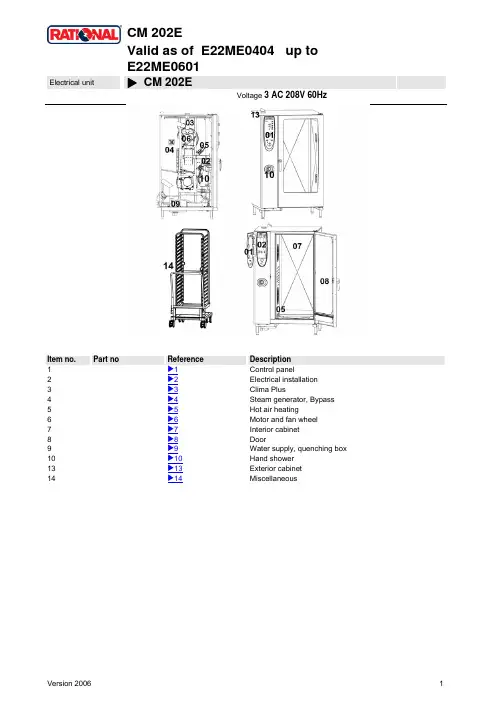
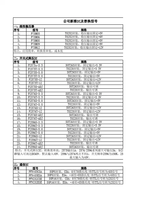
CM 202EValid as of E22ME0404 up toE22ME0601Electrical unit X CM 202EVoltage 3 AC 208V 60HzItem no. Part no Reference Description1 X1Control panel2 X2Electrical installation3 X3Clima Plus4 X4Steam generator, Bypass5 X5Hot air heating6 X6Motor and fan wheel7 X7Interior cabinet8 X8Door9 X9Water supply, quenching box10 X10Hand shower13 X13Exterior cabinet14 X14MiscellaneousCM 202EElectrical unit X Table of contentsVoltage: 3 AC 208V 60Hz1 Control panel (3)1.A Control panel (4)2 Electrical installation (5)2.A Contactor assembly (6)3 Clima Plus (8)4 Steam generator, Bypass (9)4.A Pump connection spout cpl (10)4.B Venting valve for steam generator (11)5 Hot air heating (12)6 Motor and fan wheel (13)7 Interior cabinet (14)7.A Interior cabinet welded (15)7.B Gasket frame w. glass a. gaskets (16)7.C Air baffle (17)7.C Air baffle (18)8 Door (19)8.A Door (21)8.C Door catch (22)9 Water supply, quenching box (23)10 Hand shower (24)13 Exterior cabinet (25)13.A Exterior cabinet (26)14 Miscellaneous (27)Electrical unit X 1 Control panel 11 Control panel Voltage 3 AC 208V 60HzItem no. Part no Reference DescriptionA X1.A Control panel1 87.00.001Control panel insert with overlayElectrical unit X 1.A Control panel 11 Control panel Voltage 3 AC 208V 60HzItem no. Part no Reference Description1 42.00.004 Control pcb Index "ME"2 1104.0121Hex nut M4 self locking3 10.00.355Spacer black4 2020.0400Fixing device for cable harness5 16.00.282Dial6 40.02.087 Buzzer6 3006.0107 Buzzer7 5110.1028 Gasket poti hot air, core temperature8 40.00.464Potentiometer CT9 16.00.387Mounting device f.sealing + sealing lip10 1306.0218Washer A4,311 1103.0122Hex nut M3 self-locking12 5110.1029Gasket mode switch13 5110.1027Distance plate for front panelElectrical unit X 2 Electrical installation 22 Electrical installation Voltage3 AC 208V 60HzItem no. Part no Reference DescriptionA X2.A Contactor assembly1 4007.0620Membrane DGC 292 10.00.418 Bundle guide big3 40.00.453Solid state relais4 10.00.507Pan head screw Torx 5/16" T205 10.00.444Raised countersunk head screw Torx M4x86 1106.0224Hex nut M6 self locking7 10.00.065Countersunk screw Torx T20 M4x128 1104.0122Hex combination nut M4 galv9 42.00.007 External memory10 10.00.510Grommet 10/12/16-211 1104.0801Cage nut M412 10.00.243Spacer M4x813 1104.0120Hex nut M414 10.00.112Cable clip short15 10.00.111Cable clip long16 10.00.471Cable clip d10-12mm17 40.00.338Sicotronic-terminal *screw typ*19 40.01.356Fixing device f. cable guide20 1106.0160Hex nut M621 1206.0120Tooth lock washer A6,422 40.01.132Center fixation f. contactor assembly23 40.00.471Bus cable 0.8m23 40.00.472Bus cable 1.3m26 1104.0400Rivet nut M4Electrical unit X 2.A Contactor assembly 22 Electrical installation Voltage3 AC 208V 60HzItem no. Part no Reference Description1 40.01.329Dry up protector 160°2 3014.0302Hex nut M10 for dry-up protector3 40.01.482Safety temperature limiter 365°C4 3014.0327Hex nut M10x1,05 40.00.576 Contactor CK08CA311N-M6 40.00.474Cooling fan D.C.7 10.00.238Screw Torx 4x508 3101.1008Cooling fan9 40.00.333Halogen transformer10 40.01.613Varistor11 40.00.592Transformer f. cooling fan12 1105.0120 Hex nut M513 1305.0160Washer A5,3x10mm14 4001.1203End plate for mounting rail15 2620.370233Installation rail for Contactor 100mm15 2816.1307 Installation rail for Contactor 140mm16 10.00.061Pan head screw Torx T20 M4x1217 10.00.111Cable clip long18 40.01.588Fuse SC-8A 10x3819 40.01.487Fuse holder 2pol20 10.00.364Pan head screw Torx M3x1221 4001.0217Fuse SC 60A22 40.01.489Fuse holder 3pol23 40.01.488Fuse holder 2pol24 40.01.610Earth terminal 20 WKN 70SL/U25 40.01.609Terminal block grey WKN 150/U26 40.01.611Terminal block grey WKN 70/U27 10.00.244 - Unterlegscheibe A3.228 40.00.212Cable buzzerElectrical unit X 2.A Contactor assembly 22 Electrical installation Voltage3 AC 208V 60HzItem no. Part no Reference Description28 40.01.475Cable clock switch USA28 40.00.250Cable contactor-SSR28 40.01.271Cable control harness28 40.00.243Cable control SSR28 40.00.205Cable level electrode28 40.00.219Cable SC pump28 40.00.220Cable solenoid valveElectrical unit X 3 Clima Plus 33 Clima Plus Voltage 3 AC 208V 60HzItem no. Part no Reference Description1 22.00.324Safety valve2 22.00.214 Hose d50x2023 2066.0531Hose clamp ø564 2001.0124Compression springElectrical unit X 4 Steam generator, Bypass 44 Steam generator, Bypass Voltage 3 AC 208V 60HzItem no. Part no Reference DescriptionA 8354.1320X4.A Pump connection spout cpl.B 8354.1304X4.B Venting valve for steam generator1 3002.0402Filling level electrode 90 mm2 44.00.175 Steam generator insolated3 1106.0803Hex combination nut M6 galv4 44.00.527 Heating element5 44.00.279Gasket f. heating element6 2066.0519Hose clamp 35,6mm7 2066.0526Hose clamp ø46mm8 44.00.207 Emptying pump9 1006.0762Hex screw M6x1010 1306.0222Washer A6,4x15x1,511 44.00.232Fixing device f. pump steam generator12 44.00.242Drain hose steam generator13 2066.0518Hose clamp 30mm14 40.00.291Thermocouple steam generator15 1104.0122Hex combination nut M4 galv16 44.00.362Steam hose 70x517 2066.0505Hose clamp 70-90mm18 2066.0506Hose clamp 20-32mm19 1105.0120 Hex nut M520 1205.0120 Tooth lock washer A5,321 2066.0300Hose clamp 50-70 mm22 2920.1300Level elektrode insert24 10.00.414Cable strap black 120°25 44.00.280Gasket f. heating element+Level elektrode insertElectrical unit X 4.A Pump connection spout cpl. 44 Steam generator, Bypass Voltage 3 AC 208V 60HzItem no. Part no Reference Description1 2118.1000Pump connection spout2 2120.1259Stop plug 10mm3 2066.0527Hose clamp ø14mm4 2066.0530Hose clamp ø16.4mm5 2062.0331Junction pressure hose GS 106 4005.0101Tie rap 145 mmElectrical unit X 4.B Venting valve for steam generator 44 Steam generator, Bypass Voltage 3 AC 208V 60HzItem no. Part no Reference Description1 2062.0332Receptacle for ventilation valve SG2 2069.0108Ventilation valve3 2112.1310Form hose for ventilation of steam generator4 2066.0506Hose clamp 20-32mmElectrical unit X 5 Hot air heating 55 Hot air heating Voltage 3 AC 208V 60HzItem no. Part no Reference Description1 40.00.330Mating flange f. heating assembly2 40.00.258 Heating assembly3 10.00.109Hex screw M5x234 1106.0360Cap nut M6, high shape5 1306.0222Washer A6,4x15x1,56 40.00.331Gasket f. heating assemblyElectrical unit X 6 Motor and fan wheel 66 Motor and fan wheel Voltage 3 AC 208V 60HzItem no. Part no Reference Description1 2120.1306Spacer SW19x172 22.00.123Flange f. motor shaft gasket3 22.00.120Mounting support f. gasket flange4 22.00.083 Motor shaft gasket4 5001.0207 Motor shaft gasket5 1315.0101Copper washer 6x10⁶ 1106.0220Hex nut M6 flat7 22.00.192Fan weel d340x1358 1008.0763Hex screw M8x208 10.00.565 Hex screw M8x2010 40.00.435Exhaust channel f. SSR11 40.00.274 Fan motor11 40.00.275 Fan motor12 10.00.071Hex nut M812 1108.0260Hex nut M812 10.00.710Hex nut M8 w. locking13 1208.0260Spring washer B814 1008.1005Square necked mushroom head bolt 8x40Electrical unit X 7 Interior cabinet 77 Interior cabinet Voltage 3 AC 208V 60HzItem no. Part no Reference DescriptionA X7.A Interior cabinet weldedB 40.00.091X7.B Gasket frame w. glass a. gasketsC 22.00.462 X7.C Air baffleC 22.00.298 X7.C Air baffle1 40.00.520 Screen interior cabinet sensor3 3024.0201Halogen bulb for interior cabinet 300°C4 40.00.229 Wiring interior light5 20.00.399 Door gasket6 40.01.943 Meat probe sensor6 40.02.103 Meat probe sensor6 40.00.298 Meat probe sensor7 1315.0104Copper washer 16x20x1,58 10.00.422 Hex nut M169 3014.0162Sealing cone for thermocouple10 3014.0163Gasket sleeve with nipple11 22.00.222Air baffle support12 40.00.594Thermocouple interior cabinet B113 2005.0308Outlet sieveElectrical unit X 7.A Interior cabinet welded 77 Interior cabinet Voltage 3 AC 208V 60HzItem no. Part no Reference Description1 40.00.098Reflector f. interior light2 4001.1248 Porcelain connector 2-pin interior light3 2120.1277Base for sensor connection4 1603.0167 Tubular rivet 3,2x0.25x105 10.00.041Rivet nut M5 hexagon closedElectrical unit X 7.B Gasket frame w. glass a. gaskets 77 Interior cabinet Voltage 3 AC 208V 60HzItem no. Part no Reference Description1 40.00.093Outer gasket f. interior light2 40.00.094Inner gasket f. interior light3 40.00.095Glass pane f. interior light4 40.00.096 Gasket frame f. interior light5 10.00.682 Phillips countersunk-head screw M5x16Electrical unit X 7.C Air baffle 77 Interior cabinet Voltage 3 AC 208V 60HzItem no. Part no Reference Description1 40.01.289Fixing clip core temp. cable2 1304.0160Washer A4,33 1604.0167Rivet 4x10⁴ 22.00.332Air sucking ring f. air baffle5 2760.1370Latch hook for air baffle6 10.00.515Rivet 3,2x5 A4Electrical unit X 7.C Air baffle 77 Interior cabinet Voltage 3 AC 208V 60HzItem no. Part no Reference Description1 1304.0160Washer A4,32 1604.0167Rivet 4x10³ 22.00.332Air sucking ring f. air baffle4 2760.1370Latch hook for air baffle5 40.01.289Fixing clip core temp. cable6 10.00.515Rivet 3,2x5 A46 1603.0166Rivet 3,2x7,9 CNS closed7 1603.0168Rivet 3,2x8 A48 22.00.440 Guard plate f. core sensorElectrical unit X 8 Door 88 Door Voltage 3 AC 208V 60HzItem no. Part no Reference DescriptionA 24.00.126X8.A DoorC 8514.1307X8.C Door catch1 2001.0042Loctite 243 10 ml2 2001.0046 Loctite 2723 24.00.136Door handle4 8474.1410Door lock5 1005.1901Straight pin ø5,6x166 1006.0761Hex screw M6x126 10.00.698Hex screw M6x12 w. precoat 857 1206.0261Spring washer B68 2940.1305Door bolt9 1008.1963Hex socket countersunk head screw M8x1610 2039.0309Cover cap for door11 1004.0665Allen screw M4x611 10.00.696Allen screw M4x6 w. Precoat 8512 24.00.133Door mounting support top13 1008.0768Ornamental screw M8x1614 1308.0160Washer A8,415 24.00.145Door bolt16 1008.0766Hex screw M8x3017 1308.0162Washer A8,418 24.00.048Door bolt19 1008.0769Ornamental screw M8x3020 2001.0109Compression spring21 1008.0761Hex screw M8x2522 1208.0260Spring washer B823 24.00.216Mounting braket f. door lock24 1008.0752Hex screw M5x1024 10.00.697Hex screw M5x10 w. precoat 85Electrical unit X 8 Door 88 Door Voltage 3 AC 208V 60HzItem no. Part no Reference Description25 1305.0160Washer A5,3x10mm26 10.00.099 Hex screw M8x1227 1005.1903Straight pin ø5,6x1228 1004.0906 Hex socket set screw M4x8Electrical unit X 8.A Door 88 Door Voltage 3 AC 208V 60HzItem no. Part no Reference Description1 24.00.212Inner glass pane2 24.00.147Sleeve for door bolt top3 24.00.159Door setting bolt4 24.00.503Fixing device f. magnet with magnet5 24.00.194Gasket glass pane/trolly6 24.00.178Pre heat mechanism f. door cpl.7 24.00.507Fixing device middle f.inter. glass pane8 24.00.701Additional gasket f. trolly9 24.01.259Plastic buffer 8,1mmElectrical unit X 8.C Door catch 88 Door Voltage 3 AC 208V 60HzItem no. Part no Reference Description1 5012.0711Silicone plate for door2 1006.1000 Stud bolt M6x753 1306.0550Washer A6,64 1004.0904Hex socket set screw M6x105 1106.0160Hex nut M66 2001.0119 Compression spring f. door catch7 1006.0625Allen screw M6x70Electrical unit X 9 Water supply, quenching box 99 Water supply, quenchingVoltage 3 AC 208V 60HzboxItem no. Part no Reference Description1 54.00.210Exhaust pipe2 2066.0516Hose clamp 60-80 mm3 40.00.398 Thermocouple quenching4 50.00.316Single solenoid valve5 50.00.139Single solenoid valve6 50.00.073Water distribution vert w/o roll guide con.7 50.00.072Water distribution vert roll guide con.8 50.00.277 Mounting device f. water distribution9 50.00.086Locking plate f. water distribution10 50.00.078Non return valve DW16/DN1211 1900.0202Water filter12 2067.0050Pressure hose d10mm13 2066.0205Hose clamp 8-16x9 mm SW 7mm14 8664.1301T-fitting water connection15 5110.1024Gasket for G3/4" threaded joint16 50.00.085Plug-in spring f. hand shower roll guide17 54.00.237 Inspection lid f. quenching chamber18 5012.0566Gasket quenching chamber 0-ring19 54.00.225Clamping bar20 2016.0943Quenching nozzle21 2112.1307Hose 70x5mmElectrical unit X 10 Hand shower 1010 Hand shower Voltage 3 AC 208V 60HzItem no. Part no Reference Description1 50.00.176 Hand shower roll guide2 50.00.230Connect. pipe f. hand shower roll guide3 50.00.130Hand shower4 50.00.156Clamp f. hand shower roll guide5 1107.0100Star lock ø46 50.00.135 Tulip for handshower7 50.00.544 Mounting device f. hand sh. roll guide8 50.00.290Gasket f. tulip9 50.00.297Gasket f. tulip11 50.00.548Hose ø10x2x500 f. hand shower12 50.00.537Gasket f. connect.pipe hand shower roll guide13 50.00.538O-ring f. connect. pipe f. hand shower roll guideElectrical unit X 13 Exterior cabinet 1313 Exterior cabinet Voltage 3 AC 208V 60HzItem no. Part no Reference DescriptionA X13.A Exterior cabinet1 22.00.354Spacer ring1 8450.1310 Spacer ring2 22.00.353Vent cover2 8455.1209 Vent cover3 2022.0101Grommet 18 mm4 8700.0317Floor fixing for units6 5006.0213Glue for floor fixing brackets7 5013.0100Edge protection profile10 2039.0111Foot adjustable, metal, 40 x 40Electrical unit X 13.A Exterior cabinet 1313 Exterior cabinet Voltage 3 AC 208V 60HzItem no. Part no Reference Description1 16.00.332Top cover2 1003.2265Countersunk self tapping screw 4,2x163 1104.0820Snap nut 4,2mm4 16.00.158Side panel right5 1603.0166Rivet 3,2x7,9 CNS closed6 16.00.139Side panel left7 10.00.102Hex self tapping screw B4,2x328 16.00.198Back panel9 16.00.296Front panel10 2002.0107Tension spring for front panel11 16.00.673 Air inlet filter12 2039.0331Cap for service door13 16.00.331Crossbar top14 5105.1028Gasket f. breather tube d=74mm15 16.00.360Cover f. RS232 interface16 10.00.103EJOT PT-screw KA 3.5x10¹⁷ 16.00.338 Edge protection profile18 16.00.115Rosette19 16.00.358Crossbar front panel20 40.00.454Door switch 1.65m22 16.00.384Bracket for door contact switch23 40.00.476Exhaust channelElectrical unit X 14 Miscellaneous 1414 Miscellaneous Voltage 3 AC 208V 60HzItem no. Part no Reference Description1 60.22.086 Mobile oven rack for type 202,2 1008.0760Hex screw M8x163 10.00.357Rubber plug black4 10.00.448 Phillips countersunk-head screw M5x165 1008.0750Hex screw M5x166 1006.0760Hex screw M6x167 10.00.565 Hex screw M8x208 1208.0160Tooth lock washer A8,49 1104.0400Rivet nut M410 1306.0120Washer A6,412 60.60.100Castor with brake ø125mm13 60.60.101Castor without brake ø125mm14 1603.0162 Rivet 3,2x915 42.00.030 Memory-Stick16 4019.0008 Sticker Electric/Danger17 60.60.574Positioning support f. core sensor。
_______________General DescriptionThe MAX753/MAX754 drive cold-cathode fluorescent lamps (CCFLs) and provide the LCD backplane bias (contrast) power for color or monochrome LCD panels.These ICs are designed specifically for backlit note-book-computer applications.Both the backplane bias and the CCFL supply can be shut down independently. When both sections are shut down, supply current drops to 25µA. The LCD contrast and CCFL brightness can be adjusted by clocking sep-arate digital inputs or using external potentiometers.LCD contrast and backlight brightness settings are pre-served in their respective counters while in shutdown.On power-up, the LCD contrast counter and CCFL brightness counter are set to one-half scale.The ICs are powered from a regulated 5V supply. The magnetics are connected directly to the battery, for maximum power efficiency.The CCFL driver uses a Royer-type resonant architec-ture. It can provide from 100mW to 6W of power to one or two tubes. The MAX753 provides a negative LCD bias voltage; the MAX754 provides a positive LCD bias voltage.________________________ApplicationsNotebook Computers Palmtop Computers Pen-Based Data Systems Personal Digital Assistants Portable Data-Collection Terminals____________________________Features♦Drives Backplane and Backlight ♦4V to 30V Battery Voltage Range ♦Low 500µA Supply Current♦Digital or Potentiometer Control of CCFL Brightness and LCD Bias Voltage ♦Negative LCD Contrast (MAX753)♦Positive LCD Contrast (MAX754)♦Independent Shutdown of Backlight and Backplane Sections ♦25µA Shutdown Supply Current______________Ordering Information* Contact factory for dice specifications.MAX753/MAX754CCFL Backlight and LCD Contrast Controllers________________________________________________________________Maxim Integrated Products1__________________Pin Configuration19-0197; Rev 1; 1/95For pricing, delivery, and ordering information, please contact Maxim Direct at 1-888-629-4642,or visit Maxim’s website at .M A X 753/M A X 754CCFL Backlight andLCD Contrast Controllers 2_______________________________________________________________________________________ABSOLUTE MAXIMUM RATINGSELECTRICAL CHARACTERISTICS(V DD = 5V, BATT = 15V, CON = LON = 5V, LX = G ND = PG ND = 0V, I REF = 0mA, all digital input levels are 0V or 5V, T A = T MIN to T MAX , unless otherwise noted.)Stresses beyond those listed under “Absolute Maximum Ratings” may cause permanent damage to the device. These are stress ratings only, and functional operation of the device at these or any other conditions beyond those indicated in the operational sections of the specifications is not implied. Exposure to absolute maximum rating conditions for extended periods may affect device reliability.V DD to GND.................................................................-0.3V, +7V PGND to GND.....................................................................±0.3V BATT to GND.............................................................-0.3V, +36V LX to GND............................................................................±50V CS to GND.....................................................-0.6V, (V DD + 0.3V)Inputs/Outputs to GND (LADJ, CADJ, LON,CON, REF, CFB, CC, CDRV, LDRV, LFB).....-0.3V, (V DD + 0.3V)Continuous Power Dissipation (T A = +70°C)Plastic DIP (derate 10.53mW/°C above +70°C)...........842mW Narrow SO (derate 8.70mW/°C above +70°C).............696mWOperating Temperature RangesMAX75_C_ _........................................................0°C to +70°C MAX75_E_ _......................................................-40°C to +85°C Junction Temperature......................................................+150°C Storage Temperature Range.............................-65°C to +160°C Lead Temperature (soldering, 10sec).............................+300°CMAX753/MAX754CCFL Backlight and LCD Contrast Controllers_______________________________________________________________________________________3Note 1:Maximum shutdown current occurs at BATT = LX = 0V.Note 2:Timing specifications are guaranteed by design and not production tested.ELECTRICAL CHARACTERISTICS (continued)(V DD = 5V, BATT = 15V, CON = LON = 5V, LX = G ND = PG ND = 0V, I REF = 0mA, all digital input levels are 0V or 5V, T A = T MIN to T MAX , unless otherwise noted.)M A X 753/M A X 754CCFL Backlight andLCD Contrast Controllers 4_____________________________________________________________________________________________________________________________________________________Pin Description_______________Theory of OperationCCFL InverterThe MAX753/MAX754’s CCFL inverter is designed to drive one or two cold-cathode fluorescent lamps (CCFLs) with power levels from 100mW to 6W. These lamps commonly provide backlighting for LCD panels in portable computers.Drive Requirements for CCFL TubesCCFL backlights require a high-voltage, adjustable AC power source. The MAX753/MAX754 generate this AC waveform with a self-oscillating, current-fed, parallel resonant circuit, also known as a Royer-type oscillator. Figure 1 shows one such circuit. The Royer oscillator is comprised of T1, C9, the load at the secondary, Q4,and Q5. The circuit self-oscillates at a frequency deter-mined by the effective primary inductance and capaci-tance. Q4 and Q5 are self-driven by the extra winding.The current source feeding the Royer oscillator is com-prised of L1, D5, and the MAX758A. When current from the current source increases, so does the lamp current.The lamp current is half-wave rectified by D7A andD7B, and forms a voltage across resistor R8. The MAX753’s error amplifier compares the average of this voltage to the output of its internal DAC. Adjusting the DAC output from zero scale to full scale (digital control)causes the error amplifier to vary the tube current from a minimum to a maximum. The DAC’s transfer function is shown in Figure 2.On power-up or after a reset, the counter sets the DAC output to mid scale. Each rising edge of CADJ (with CON high) decrements the DAC output. When decre-mented beyond full scale, the counter rolls over and sets the DAC to the maximum value. In this way, a sin-gle pulse applied to CADJ decreases the DAC set-point by one step, and 31 pulses increase the set-point by one step.The error amplifier’s output voltage controls the peak current output of the MAX758A. The peak switch cur-rent is therefore controlled by the output of the error amplifier. The lower the error amplifier’s output, the lower the peak current. Since the current through the current source is related to the current through the tube, the lower the error amplifier’s output, the lower the tube current.MAX753/MAX754CCFL Backlight and LCD Contrast Controllers_______________________________________________________________________________________5Figure 1. CCFL and Positive LCD Power SupplyM A X 753/M A X 754CCFL Backlight andLCD Contrast Controllers 6_______________________________________________________________________________________In Figure 1, the MAX758A, L1, and D5 form a voltage-controlled switch-mode current source. The current out of L1 is proportional to the voltage applied to the SS pin. The MAX758A contains a current-mode pulse-width-modulating buck regulator that switches at 170kHz. The voltage on the SS pin sets the switch cur-rent limit and thus sets the current out of L1.CCFL Current-Regulation LoopFigure 3 shows a block diagram of the regulation loop,which maintains a fixed CCFL average lamp current despite changes in input voltage and lamp impedance.This loop regulates the average value of the half-wave rectified lamp current. The root mean square lamp cur-rent is related to, but not equal to, the average lamp current. Assuming a sinusoidal lamp current, select R8where V REF = 1.25V and I LAMP,RMS is the desired full-scale root mean square lamp current.Figure 2. CCFT DAC Transfer FunctionFigure 3. CCFL Tube Current-Regulation LoopThe minimum operating input voltage is determined by the transformer turns ratio (n), the lamp operating volt-age (V LAMP ), and the ballast capactor (C10). Using a simple model of the CCFL (see Figure 4) we can calcu-late what the T1 center-tap voltage will be at maximum lamp current. The voltage on the CCFL is in phase with the current through it. Let us define I LAMP (t) =LAMP,RMS cos(ωt) and V LAMP (t) = √LAMP,RMS cos(ωt); then the peak voltage at the center tap will bewhere,n is the secondary-to-primary turns ratio of T1, and ω is the frequency of Royer oscillation in radians per sec-ond. The voltage on the center tap of T1 is a full-wave rectified sine wave (see Figure 5). The average voltage at V TAP must equal the average voltage at the LX node of the MAX758A, since there cannot be any DC voltage on inductor L1; thus the minimum operating voltage must be greater than the average voltage at V TAP .LCD Bias GeneratorsThe MAX753/MAX754’s LCD bias generators provide adjustable output voltages for powering LCD displays.The MAX753’s LCD converter generates a negative output, while the MAX754’s generates a positive output.The MAX753/MAX754 employ a constant-peak-currentpulse-frequency-modulation (PFM) switching regulator.The MAX753 adds a simple diode-capacitor voltage inverter to the switching regulator.Constant-Current PFM Control SchemeThe LCD bias generators in these devices use a con-stant-peak-current PFM control scheme. Figure 6, which shows the MAX754’s boost switching regulator, illus-trates this control method. When Q3 closes (Q3 “on”) a voltage equal to BATT is applied to the inductor, caus-ing current to flow from the battery, through the inductor and switch, and to ground. This current ramps up linear-ly, storing energy in the inductor’s magnetic field. When Q3 opens, the inductor voltage reverses, and current flows from the battery, through the inductor and diode,and into the output capacitor. The devices regulate the output voltage by varying how frequently the switch is opened and closed.The MAX753/MAX754 not only regulate the output volt-age, but also maintain a constant peak inductor cur-rent, regardless of the battery voltage. The ICs vary the switch on-time to produce the constant peak current,and vary its off-time to ensure that the inductor current reaches zero at the end of each cycle.The internal circuitry senses both the output voltage and the voltage at the LX node, and turns on the MOS-FET only if: 1) The output voltage is out of regulation,and 2) the voltage at LX is less than the battery voltage.The first condition keeps the output in regulation, and the second ensures that the inductor current always resets to zero (i.e., the part always operates in discon-tinuous-conduction mode).MAX753/MAX754CCFL Backlight and LCD Contrast Controllers_______________________________________________________________________________________7Figure 4. Simple Model of the CCFL Figure 5. Voltage at the Center Tap of T1M A X 753/M A X 754CCFL Backlight andLCD Contrast Controllers 8_______________________________________________________________________________________Figure 6. MAX754 Positive LCD-Bias GeneratorTable 1. CCFL Circuit Component DescriptionsITEMDESCRIPTIONC5Integrating Capacitor. 1 / (C5 x R18) sets the dominant pole for the feedback loop, which regulates the lamp current. Set the dominant pole at least two decades below the Royer frequency to eliminate the AC compo-nent of the voltage on R8. For example, if your Royer is oscillating at 50kHz = 314159rad/s, you should set 1 / (C5 x R18) ≤3142rad/s.R18Integrating Resistor. The output source-current capability of the CC pin (50µA) limits how small R18 can be.Do not make R18 smaller than 70k Ω, otherwise CC will not be able to servo CFB to the DAC voltage (i.e., the integrator will not be able to integrate) and the loop will not be able to regulate.R8R8 converts the half-wave rectified lamp current into a voltage. The average voltage on R8 is not equal to the root mean square voltage on R8. The accuracy of R8 is important since it, along with the MAX754 reference,sets the full-scale lamp current. Use a ±1%-accurate resistor.D7A, D7BD7A and D7B half-wave rectify the CCFL lamp current. Half-wave rectification of the lamp current and then averaging is a simple way to perform AC-to-DC conversion. D7A and D7B’s forward voltage drop and speed are unimportant; they do not need to pass currents larger than about 10mA, and their reverse breakdown voltage can be as low as 10V.CCFLThe circuit of Figure 1, with the components shown in the bill of materials (Table 4), will drive a 500V RMS oper-ating cold-cathode fluorescent lamp at 6W of power with a +12V input voltage. The lower the input voltage,the less power the circuit can deliver.MAX753/MAX754CCFL Backlight and LCD Contrast Controllers_______________________________________________________________________________________9Table 1. CCFL Circuit Component Descriptions (continued)M A X 753/M A X 754CCFL Backlight andLCD Contrast Controllers 10______________________________________________________________________________________Table 2. CCFL Circuit Design Example (Note 1)Note 1:To perform your own calculations for the parameters given in Table 2 (Design Example), use the equations given in Table 3 (Design Equations). Note 2:T1 = Sumida’s EPS207Note 3:C9 = Wima’s SMD 7.3 __/63分销商库存信息:MAXIMMAX753ESE+MAX754ESE+MAX753ESE+T MAX754ESE+T。
________________________________________________________________Maxim Integrated Products 1General DescriptionThe MAX202E–MAX213E, MAX232E/MAX241E line drivers/receivers are designed for RS-232 and V.28communications in harsh environments. Each transmitter output and receiver input is protected against ±15kV electrostatic discharge (ESD) shocks, without latchup.The various combinations of features are outlined in the Selector Guide.The drivers and receivers for all ten devices meet all EIA/TIA-232E and CCITT V.28specifications at data rates up to 120kbps, when loaded in accordance with the EIA/TIA-232E specification.The MAX211E/MAX213E/MAX241E are available in 28-pin SO packages, as well as a 28-pin SSOP that uses 60% less board space. The MAX202E/MAX232E come in 16-pin TSSOP, narrow SO, wide SO, and DIP packages. The MAX203E comes in a 20-pin DIP/SO package, and needs no external charge-pump capacitors. The MAX205E comes in a 24-pin wide DIP package, and also eliminates external charge-pump capacitors. The MAX206E/MAX207E/MAX208E come in 24-pin SO, SSOP, and narrow DIP packages. The MAX232E/MAX241E operate with four 1µF capacitors,while the MAX202E/MAX206E/MAX207E/MAX208E/MAX211E/MAX213E operate with four 0.1µF capacitors,further reducing cost and board space.________________________ApplicationsNotebook, Subnotebook, and Palmtop Computers Battery-Powered Equipment Hand-Held EquipmentNext-Generation Device Featureso For Low-Voltage ApplicationsMAX3222E/MAX3232E/MAX3237E/MAX3241E/MAX3246E: ±15kV ESD-Protected Down to10nA, +3.0V to +5.5V, Up to 1Mbps, True RS-232Transceivers (MAX3246E Available in a UCSP™Package)o For Low-Power ApplicationsMAX3221/MAX3223/MAX3243: 1µA SupplyCurrent, True +3V to +5.5V RS-232 Transceivers with Auto-Shutdown™o For Space-Constrained ApplicationsMAX3233E/MAX3235E: ±15kV ESD-Protected,1µA, 250kbps, +3.0V/+5.5V, Dual RS-232Transceivers with Internal Capacitorso For Low-Voltage or Data Cable ApplicationsMAX3380E/MAX3381E: +2.35V to +5.5V, 1µA,2Tx/2Rx RS-232 Transceivers with ±15kV ESD-Protected I/O and Logic PinsMAX202E–MAX213E, MAX232E/MAX241E±15kV ESD-Protected, +5V RS-232 TransceiversSelector Guide19-0175; Rev 6; 3/05Pin Configurations and Typical Operating Circuits appear at end of data sheet.YesPARTNO. OF RS-232DRIVERSNO. OF RS-232RECEIVERSRECEIVERS ACTIVE IN SHUTDOWNNO. OF EXTERNAL CAPACITORS(µF)LOW-POWER SHUTDOWNTTL TRI-STATE MAX202E 220 4 (0.1)No No MAX203E 220None No No MAX205E 550None Yes Yes MAX206E 430 4 (0.1)Yes Yes MAX207E 530 4 (0.1)No No MAX208E 440 4 (0.1)No No MAX211E 450 4 (0.1)Yes Yes MAX213E 452 4 (0.1)Yes Yes MAX232E 220 4 (1)No No MAX241E454 (1)YesFor pricing, delivery, and ordering information,please contact Maxim/Dallas Direct!at 1-888-629-4642, or visit Maxim’s website at .AutoShutdown and UCSP are trademarks of Maxim Integrated Products, Inc.Ordering InformationOrdering Information continued at end of data sheet.2_______________________________________________________________________________________M A X 202E –M A X 213E , M A X 232E /M A X 241EABSOLUTE MAXIMUM RATINGSV CC ..........................................................................-0.3V to +6V V+................................................................(V CC - 0.3V) to +14V V-............................................................................-14V to +0.3V Input VoltagesT_IN............................................................-0.3V to (V+ + 0.3V)R_IN...................................................................................±30V Output VoltagesT_OUT.................................................(V- - 0.3V) to (V+ + 0.3V)R_OUT......................................................-0.3V to (V CC + 0.3V)Short-Circuit Duration, T_OUT....................................Continuous Continuous Power Dissipation (T A = +70°C)16-Pin Plastic DIP (derate 10.53mW/°C above +70°C)....842mW 16-Pin Narrow SO (derate 8.70mW/°C above +70°C).....696mW 16-Pin Wide SO (derate 9.52mW/°C above +70°C)......762mW 16-Pin TSSOP (derate 9.4mW/°C above +70°C)...........755mW20-Pin Plastic DIP (derate 11.11mW/°C above +70°C)...889mW 20-Pin SO (derate 10.00mW/°C above +70°C).............800mW 24-Pin Narrow Plastic DIP(derate 13.33mW/°C above +70°C) ...............................1.07W 24-Pin Wide Plastic DIP(derate 14.29mW/°C above +70°C)................................1.14W 24-Pin SO (derate 11.76mW/°C above +70°C).............941mW 24-Pin SSOP (derate 8.00mW/°C above +70°C)..........640mW 28-Pin SO (derate 12.50mW/°C above +70°C)....................1W 28-Pin SSOP (derate 9.52mW/°C above +70°C)..........762mW Operating Temperature RangesMAX2_ _EC_ _.....................................................0°C to +70°C MAX2_ _EE_ _...................................................-40°C to +85°C Storage Temperature Range.............................-65°C to +165°C Lead Temperature (soldering, 10s).................................+300°CELECTRICAL CHARACTERISTICS(V CC = +5V ±10% for MAX202E/206E/208E/211E/213E/232E/241E; V CC = +5V ±5% for MAX203E/205E/207E; C1–C4 = 0.1µF for MAX202E/206E/207E/208E/211E/213E; C1–C4 = 1µF for MAX232E/241E; T A = T MIN to T MAX ; unless otherwise noted. Typical values are at T A = +25°C.)Stresses beyond those listed under “Absolute Maximum Ratings” may cause permanent damage to the device. These are stress ratings only, and functional operation of the device at these or any other conditions beyond those indicated in the operational sections of the specifications is not implied. Exposure to absolute maximum rating conditions for extended periods may affect device reliability.ELECTRICAL CHARACTERISTICS (continued)MAX202E–MAX213E, MAX232E/MAX241E (V CC= +5V ±10% for MAX202E/206E/208E/211E/213E/232E/241E; V CC= +5V ±5% for MAX203E/205E/207E; C1–C4 = 0.1µF forMAX202E/206E/207E/208E/211E/213E; C1–C4 = 1µF for MAX232E/241E; T A= T MIN to T MAX; unless otherwise noted. Typical valuesare at T A= +25°C.)Note 1:MAX211EE_ _ tested with V CC= +5V ±5%._______________________________________________________________________________________34______________________________________________________________________________________M A X 202E –M A X 213E , M A X 232E /M A X 241E__________________________________________Typical Operating Characteristics(Typical Operating Circuits, V CC = +5V, T A = +25°C, unless otherwise noted.)5.00MAX211E/MAX213ETRANSMITTER OUTPUT VOLTAGEvs. LOAD CAPACITANCELOAD CAPACITANCE (pF)V O H , -V O L (V )5.56.06.57.07.58.0100020003000400050000MAX211E/MAX213E/MAX241E TRANSMITTER SLEW RATE vs. LOAD CAPACITANCELOAD CAPACITANCE (pF)S L E W R A T E ( V /µs )5101520253010002000300040005000_______________________________________________________________________________________5MAX202E–MAX213E, MAX232E/MAX241E____________________________Typical Operating Characteristics (continued)(Typical Operating Circuits, V CC = +5V, T A = +25°C, unless otherwise noted.)2MAX202E/MAX203E/MAX232E TRANSMITTER SLEW RATE vs. LOAD CAPACITANCELOAD CAPACITANCE (pF)S L E W R A T E ( V /µs )468101214100020003000400050005.07.5-7.53000MAX205E–MAX208ETRANSMITTER OUTPUT VOLTAGEvs. LOAD CAPACITANCE-5.02.5LOAD CAPACITANCE (pF)O U T P U T V O L T A G E (V )10002000400050000-2.54550203000MAX205E–MAX208E SUPPLY CURRENT vs. LOAD CAPACITANCE2540LOAD CAPACITANCE (pF)S U P P L Y C U R R E N T (m A )100020004000500035302.55.0-10.0180MAX205E –MAX208EOUTPUT VOLTAGE vs. DATA RATE-7.50DATA RATE (kbps)O U T P U T V O L T A G E (V )601202401503090210-2.5-5.010.07.56_______________________________________________________________________________________M A X 202E –M A X 213E , M A X 232E /M A X 241EMAX203EMAX205E_____________________________________________________________Pin DescriptionsMAX202E/MAX232E_______________________________________________________________________________________7MAX202E–MAX213E, MAX232E/MAX241EMAX208E________________________________________________Pin Descriptions (continued)MAX206EMAX207E8_______________________________________________________________________________________M A X 202E –M A X 213E , M A X 232E /M A X 241EMAX211E/MAX213E/MAX241E)(MAX205E/MAX206E/MAX211E/MAX213E/MAX241E)________________________________________________Pin Descriptions (continued)MAX211E/MAX213E/MAX241EFigure 3. Transition Slew-Rate Circuit_______________Detailed Description The MAX202E–MAX213E, MAX232E/MAX241E consist of three sections: charge-pump voltage converters, drivers (transmitters), and receivers. These E versions provide extra protection against ESD. They survive ±15kV discharges to the RS-232 inputs and outputs, tested using the Human Body Model. When tested according to IEC1000-4-2, they survive ±8kV contact-discharges and ±15kV air-gap discharges. The rugged E versions are intended for use in harsh environments or applications where the RS-232 connection is frequently changed (such as notebook computers). The standard (non-“E”) MAX202, MAX203, MAX205–MAX208, MAX211, MAX213, MAX232, and MAX241 are recommended for applications where cost is critical.+5V to ±10V Dual Charge-PumpVoltage Converter The +5V to ±10V conversion is performed by dual charge-pump voltage converters (Figure 4). The first charge-pump converter uses capacitor C1 to double the +5V into +10V, storing the +10V on the output filter capacitor, C3. The second uses C2 to invert the +10V into -10V, storing the -10V on the V- output filter capacitor, C4.In shutdown mode, V+ is internally connected to V CC by a 1kΩpull-down resistor, and V- is internally connected to ground by a 1kΩpull up resistor.RS-232 Drivers With V CC= 5V, the typical driver output voltage swing is ±8V when loaded with a nominal 5kΩRS-232 receiver. The output swing is guaranteed to meet EIA/TIA-232E and V.28 specifications that call for ±5V minimum output levels under worst-case conditions. These include a 3kΩload, minimum V CC, and maximum operating temperature. The open-circuit output voltage swings from (V+ - 0.6V) to V-.Input thresholds are CMOS/TTL compatible. The unused drivers’ inputs on the MAX205E–MAX208E, MAX211E, MAX213E, and MAX241E can be left unconnected because 400kΩpull up resistors to V CC are included on-chip. Since all drivers invert, the pull up resistors force the unused drivers’ outputs low. The MAX202E, MAX203E, and MAX232E do not have pull up resistors on the transmitter inputs._______________________________________________________________________________________9MAX202E–MAX213E, MAX232E/MAX241E10______________________________________________________________________________________M A X 202E –M A X 213E , M A X 232E /M A X 241E±15kV ESD-Protected, +5V RS-232 Transceivers When in low-power shutdown mode, the MAX205E/MAX206E/MAX211E/MAX213E/MAX241E driver outputs are turned off and draw only leakage currents—even if they are back-driven with voltages between 0V and 12V. Below -0.5V in shutdown, the transmitter output is diode-clamped to ground with a 1k Ωseries impedance.RS-232 ReceiversThe receivers convert the RS-232 signals to CMOS-logic output levels. The guaranteed 0.8V and 2.4V receiver input thresholds are significantly tighter than the ±3V thresholds required by the EIA/TIA-232E specification.This allows the receiver inputs to respond to TTL/CMOS-logic levels, as well as RS-232 levels.The guaranteed 0.8V input low threshold ensures that receivers shorted to ground have a logic 1 output. The 5k Ωinput resistance to ground ensures that a receiver with its input left open will also have a logic 1 output. Receiver inputs have approximately 0.5V hysteresis.This provides clean output transitions, even with slow rise/fall-time signals with moderate amounts of noise and ringing.In shutdown, the MAX213E’s R4 and R5 receivers have no hysteresis.Shutdown and Enable Control (MAX205E/MAX206E/MAX211E/MAX213E/MAX241E)In shutdown mode, the charge pumps are turned off,V+ is pulled down to V CC , V- is pulled to ground, and the transmitter outputs are disabled. This reduces supply current typically to 1µA (15µA for the MAX213E).The time required to exit shutdown is under 1ms, as shown in Figure 5.ReceiversAll MAX213E receivers, except R4 and R5, are put into a high-impedance state in shutdown mode (see Tables 1a and 1b). The MAX213E’s R4 and R5 receivers still function in shutdown mode. These two awake-in-shutdown receivers can monitor external activity while maintaining minimal power consumption.The enable control is used to put the receiver outputs into a high-impedance state, to allow wire-OR connection of two EIA/TIA-232E ports (or ports of different types) at the UART. It has no effect on the RS-232 drivers or the charge pumps.N ote: The enabl e control pin is active l ow for the MAX211E/MAX241E (EN ), but is active high for the MAX213E (EN). The shutdown control pin is active high for the MAX205E/MAX206E/MAX211E/MAX241E (SHDN), but is active low for the MAX213E (SHDN ).Figure 4. Charge-Pump DiagramMAX202E–MAX213E, MAX232E/MAX241EV+V-200µs/div3V 0V 10V 5V 0V -5V -10VSHDNMAX211EFigure 5. MAX211E V+ and V- when Exiting Shutdown (0.1µF capacitors)X = Don't care.*Active = active with reduced performanceSHDN E N OPERATION STATUS Tx Rx 00Normal Operation All Active All Active 01Normal Operation All Active All High-Z 1XShutdownAll High-ZAll High-ZTable 1a. MAX205E/MAX206E/MAX211E/MAX241E Control Pin ConfigurationsTable 1b. MAX213E Control Pin ConfigurationsThe MAX213E’s receiver propagation delay is typically 0.5µs in normal operation. In shutdown mode,propagation delay increases to 4µs for both rising and falling transitions. The MAX213E’s receiver inputs have approximately 0.5V hysteresis, except in shutdown,when receivers R4 and R5 have no hysteresis.When entering shutdown with receivers active, R4 and R5 are not valid until 80µs after SHDN is driven low.When coming out of shutdown, all receiver outputs are invalid until the charge pumps reach nominal voltage levels (less than 2ms when using 0.1µF capacitors).±15kV ESD ProtectionAs with all Maxim devices, ESD-protection structures are incorporated on all pins to protect against electrostatic discharges encountered during handling and assembly. The driver outputs and receiver inputs have extra protection against static electricity. Maxim’s engineers developed state-of-the-art structures to protect these pins against ESD of ±15kV without damage. The ESD structures withstand high ESD in all states: normal operation, shutdown, and powered down. After an ESD event, Maxim’s E versions keep working without latchup, whereas competing RS-232products can latch and must be powered down to remove latchup.ESD protection can be tested in various ways; the transmitter outputs and receiver inputs of this product family are characterized for protection to the following limits:1)±15kV using the Human Body Model2)±8kV using the contact-discharge method specifiedin IEC1000-4-23)±15kV using IEC1000-4-2’s air-gap method.ESD Test ConditionsESD performance depends on a variety of conditions.Contact Maxim for a reliability report that documents test set-up, test methodology, and test results.Human Body ModelFigure 6a shows the Human Body Model, and Figure 6b shows the current waveform it generates when discharged into a low impedance. This model consists of a 100pF capacitor charged to the ESD voltage of interest, which is then discharged into the test device through a 1.5k Ωresistor.S H D N ENOPERATION STATUS Tx 1–400Shutdown All High-Z 01Shutdown All High-Z 10Normal Operation 11Normal OperationAll ActiveAll Active Active1–34, 5High-Z ActiveHigh-Z High-Z High-Z Active*High-Z RxM A X 202E –M A X 213E , M A X 232E /M A X 241EIEC1000-4-2The IEC1000-4-2 standard covers ESD testing and performance of finished equipment; it does not specifically refer to integrated circuits. The MAX202E/MAX203E–MAX213E, MAX232E/MAX241E help you design equipment that meets level 4 (the highest level) of IEC1000-4-2, without the need for additional ESD-protection components.The major difference between tests done using the Human Body Model and IEC1000-4-2 is higher peak current in IEC1000-4-2, because series resistance is lower in the IEC1000-4-2 model. Hence, the ESD withstand voltage measured to IEC1000-4-2 is generally lower than that measured using the Human Body Model. Figure 7b shows the current waveform for the 8kV IEC1000-4-2 level-four ESD contact-discharge test.The air-gap test involves approaching the device with a charged probe. The contact-discharge method connects the probe to the device before the probe is energized.Machine ModelThe Machine Model for ESD tests all pins using a 200pF storage capacitor and zero discharge resistance. Its objective is to emulate the stress caused by contact that occurs with handling and assembly during manufacturing. Of course, all pins require this protection during manufacturing, not just RS-232 inputs and outputs. Therefore,after PC board assembly,theMachine Model is less relevant to I/O ports.Figure 7a. IEC1000-4-2 ESD Test ModelFigure 7b. IEC1000-4-2 ESD Generator Current WaveformFigure 6a. Human Body ESD Test ModelFigure 6b. Human Body Model Current Waveform__________Applications InformationCapacitor Selection The capacitor type used for C1–C4 is not critical for proper operation. The MAX202E, MAX206–MAX208E, MAX211E, and MAX213E require 0.1µF capacitors, and the MAX232E and MAX241E require 1µF capacitors, although in all cases capacitors up to 10µF can be used without harm. Ceramic, aluminum-electrolytic, or tantalum capacitors are suggested for the 1µF capacitors, and ceramic dielectrics are suggested for the 0.1µF capacitors. When using the minimum recommended capacitor values, make sure the capacitance value does not degrade excessively as the operating temperature varies. If in doubt, use capacitors with a larger (e.g., 2x) nominal value. The capacitors’ effective series resistance (ESR), which usually rises at low temperatures, influences the amount of ripple on V+ and V-.Use larger capacitors (up to 10µF) to reduce the output impedance at V+ and V-. This can be useful when “stealing” power from V+ or from V-. The MAX203E and MAX205E have internal charge-pump capacitors. Bypass V CC to ground with at least 0.1µF. In applications sensitive to power-supply noise generated by the charge pumps, decouple V CC to ground with a capacitor the same size as (or larger than) the charge-pump capacitors (C1–C4).V+ and V- as Power Supplies A small amount of power can be drawn from V+ and V-, although this will reduce both driver output swing and noise margins. Increasing the value of the charge-pump capacitors (up to 10µF) helps maintain performance when power is drawn from V+ or V-.Driving Multiple Receivers Each transmitter is designed to drive a single receiver. Transmitters can be paralleled to drive multiple receivers.Driver Outputs when Exiting Shutdown The driver outputs display no ringing or undesirable transients as they come out of shutdown.High Data Rates These transceivers maintain the RS-232 ±5.0V minimum driver output voltages at data rates of over 120kbps. For data rates above 120kbps, refer to the Transmitter Output Voltage vs. Load Capacitance graphs in the Typical Operating Characteristics. Communication at these high rates is easier if the capacitive loads on the transmitters are small; i.e., short cables are best.Table 2. Summary of EIA/TIA-232E, V.28 SpecificationsMAX202E–MAX213E, MAX232E/MAX241EM A X 202E –M A X 213E , M A X 232E /M A X 241E____________Pin Configurations and Typical Operating Circuits (continued)Table 3. DB9 Cable ConnectionsCommonly Used for EIA/TIAE-232E and V.24 Asynchronous Interfaces____________Pin Configurations and Typical Operating Circuits (continued)MAX202E–MAX213E, MAX232E/MAX241EM A X 202E –M A X 213E , M A X 232E /M A X 241E____________Pin Configurations and Typical Operating Circuits (continued)MAX202E–MAX213E, MAX232E/MAX241E____________Pin Configurations and Typical Operating Circuits (continued)M A X 202E –M A X 213E , M A X 232E /M A X 241E____________Pin Configurations and Typical Operating Circuits (continued)MAX202E–MAX213E, MAX232E/MAX241E____________Pin Configurations and Typical Operating Circuits (continued)M A X 202E –M A X 213E , M A X 232E /M A X 241E____________Pin Configurations and Typical Operating Circuits (continued)______________________________________________________________________________________21MAX202E–MAX213E, MAX232E/MAX241E Ordering Information (continued)*Dice are specified at T A= +25°C.M A X 202E –M A X 213E , M A X 232E /M A X 241E22________________________________________________________________________________________________________________________________________________Chip Topographies___________________Chip InformationC1-V+C1+V CC R2INT2OUT R2OUT0.117"(2.972mm)0.080"(2.032mm)V-C2+ C2-T2IN T1OUT R1INR1OUT T1INGNDR5INV-C2-C2+C1-V+C1+V CC T4OUTR3IN T3OUTT1OUT 0.174"(4.420mm)0.188"(4.775mm)T4IN R5OUT R4OUT T3IN R4IN EN (EN) SHDN (SHDN)R3OUT T2OUT GNDR1IN R1OUT T2IN R2OUTR2IN T1IN ( ) ARE FOR MAX213E ONLYTRANSISTOR COUNT: 123SUBSTRATE CONNECTED TO GNDTRANSISTOR COUNT: 542SUBSTRATE CONNECTED TO GNDMAX202E/MAX232EMAX211E/MAX213E/MAX241EMAX205E/MAX206E/MAX207E/MAX208E TRANSISTOR COUNT: 328SUBSTRATE CONNECTED TO GNDMAX202E–MAX213E, MAX232E/MAX241E Package InformationM A X 202E –M A X 213E , M A X 232E /M A X 241EPackage Information (continued)MAX202E–MAX213E, MAX232E/MAX241E±15kV ESD-Protected, +5V RS-232 TransceiversMaxim cannot assume responsibility for use of any circuitry other than circuitry entirely embodied in a Maxim product. No circuit patent licenses are implied. Maxim reserves the right to change the circuitry and specifications without notice at any time.Maxim Integrated Products, 120 San Gabriel Drive, Sunnyvale, CA 94086 408-737-7600 ____________________25©2005 Maxim Integrated ProductsPrinted USAis a registered trademark of Maxim Integrated Products, Inc.Package Information (continued)(The package drawing(s) in this data sheet may not reflect the most current specifications. For the latest package outline information go to /packages .)。
平均功率分配算法原理在大规模MIMO网络的下行链路中执行max-min和max-prod功率分配,更确切地说,与传统的面向优化的方法相比,训练深度神经网络来学习用户设备(UE)的位置和最优功率分配策略之间的映射,然后用于预测新的UE集合的功率分配曲线。与传统的优化定向方法相比,使用深度学习的方法显著提高了功率分配的复杂性-性能折衷。特别地,所提出的方法不需要计算任何统计平均值,而是需要使用标准方法来计算,并且能够保证接近最优的性能。
1 引言大规模MIMO是指一种无线网络技术,其中基站(BS s)配备了大量的天线,通过空间复用技术为众多用户设备(UE)服务。
近年来出现了令人兴奋的事态发展。
在工业上,这项技术已被纳入5G新无线电标准。
在学术界,被认为施加了根本的限制长期的试验性污染问题,终于得到了解决。
更准确地说,有些文献中表明,在最优最小均方误差(MMSE)组合/预编码和少量空间信道相关的情况下,上行链路(UL)和下行链路(DL)中的容量随天线数目的增加而增加。
结合/预编码和少量空间信道相关,在上行链路(UL)和下行链路(DL)中,容量随天线数目的增加而增加。
在这项工作中,我们使用深度学习来解决大规模MIMO网络DL中的max-min和max-prod功率分配问题。
我们受到最近机器学习技术成功应用的爆炸式增长的启发[5],它证明了深度神经网络学习丰富模式和逼近任意函数映射的能力[5],[6]。
特别地,我们的目的是证明UE的位置(可以通过全球定位系统容易的获得)可以被神经网络有效地用于获得接近最佳的性能。
除此之外,训练这样的神经网络是相当方便的,因为通过运行现成的优化算法可以容易地获得训练样本。
在文献[7]中也考虑了无线网络中无线电资源分配的深度学习,其中速率最大化的WMMSE算法已经由完全连接的前馈神经网络模拟,并且在文献[8]中,卷积神经网络用于用户- 单元关联。
2 大规模MIMO网络对具有L个小区的大规模MIMO进行深度学习,每个小区包括具有M根天线的BS和K个UEs。
5V单电源供电的【论文集】通信收发器LMS202E/LMS4852RS-232双收发器LMS202ELMS202E采用16引脚SOIC封装,可与MAXIM公司的MAX202E相互代换。
LMS202E的内部结构及典型应用电路如图1所示。
该器件内含DC-DC变换器,利用电路中的C1~C4使内部对偶充电泵为两个发送器提供±10V的双电源。
通过C1,电荷泵可将+5V的电源电压转换为+10V,并存储在C3中。
而通过C2电荷泵则可将+10V转换为-10V电压,而后再把-10V存储在C4中。
发送器输入信号可从脚11和脚10输入且两个发送器在14脚和7脚上的输出与T1A/E1A-232E电平一致。
T1和T2两个发送器的输出摆幅为±8V,开路输出电压摆幅为(V+-0.6V)~V-。
接收器的R1IN和R2IN信号从脚13和脚8输入以接收T1A/E1A信号,并从脚12和脚9输出与TTL/CMOS兼容的信号。
RS-232接收器的输入电压VRi范围为-30V~+30V,VS为5V时的输入低门限电平是1.4V,高门限电平为2V。
接收器输出电压的最大范围为-0.3V~(VS+0.3V),从输入到输出的传输延迟时间为0.08μs(典型值)。
LMS202E的所有引脚都带有ESD保护。
除了发送器输出脚(7脚和14脚)和接收器输入脚(8脚和13脚)外,其它引脚带有±2kV的人体模型(HBM)和±200V的机器模型(MM)ESD额定值。
RS-232总线引脚(7脚、8脚、13脚和14脚)带有±15kV的HBM和IEC1000-4-2的耐冲击ESD保护。
此外,总线引脚还能满足±8kV的IEC1000-4-2接触ESD保护要求。
因此,这种ESD结构在加电、断电等场合可以承受较高ESD冲击。
3LMS485低功率差分数据收发器LMS485采用8引脚DIP或SOIC封装,可与MAX485互相代换。
LMS202E15KV ESD Rated,5V Single Supply TIA/EIA-232Dual TransceiversGeneral DescriptionThe LMS202E features two transmitters and two receivers for RS-232communication.It has a DC-to-DC converter that permits the device to operate with only a single +5V power supply.The on-chip DC-to-DC converter which utilizes four external 0.1µF capacitors to generate dual internal power supplies for RS-232compatible output levels.The device meet EIA/TIA-232E and CCITT V.28specifica-tions up to 230kbits/sec.The LMS202E is available in a 16pin narrow and wide SOIC package.The transmitter outputs and receiver inputs have ±15kV electrostatic discharge (ESD)protection.The LMS202E sur-vives a ±15kV ESD event to the RS-232input and output pins when subjected according to Human Body Model or IEC 1000-4-2(EN61000-4-2),air-gap specification.It survives a ±8kV discharge when subjected to IEC 1000-4-2(EN61000-4-2),contact specification.This device is designed for use in harsh environments where ESD is a concern.Featuresn ESD protection for RS-232I/O pins—±15kV-IEC10004-2(EN61000-4-2)Contact Discharge—±8kV-IEC10004-2(EN61000-4-2)Air-Gap Discharge —±15kV Human Body Model n Single +5V power supply n 230kbps data raten On-board DC-to-DC converter n 0.1µF charge pump capacitorsn Drop-in replacement to Maxim’s MAX202EApplicationsn POS equipment (Bar code reader)n Hand-held equipmentn General purpose RS-232communicationConnection Diagram and Typical Circuit20048001March 2003LMS202E 15KV ESD Rated,5V Single Supply TIA/EIA-232Dual Transceivers©2003National Semiconductor Corporation Pin DescriptionsPin Number Pin Name Pin Function1,3C1+,C1−External capacitor connection pins.Recommended external capacitor C1=0.1µF (6.3V)2V+Positive supply for TIA/EIA-232E drivers.Recommended external capacitor C4=0.1µF (6.3V)4,5C2+,C2−External capacitor connection pins.Recommended external capacitor C2=0.1µF (16V)6V−Negative supply for TIA/EIA-232E drivers.Recommended external capacitor C3=0.1µF (16V)7,14T1out,T2outTransmitter output pins conform to TIA/EIA-232E levels.The typical transmitter output swing is ±8V when loaded 3k Ωload to ground.The open-circuit output voltage swings from (V+−0.6V)to V−8,13R1in,R2in Receiver inputs accept TIA/EIA-2329,12R1out and R2out Receiver output pins are TTL/CMOS compatible10,11Tin1,Tin2Transmitter input pins are TTL/CMOS compatible.Inputs of transmitter do not have pull-up resistors.Connect all unused transmitter inputs to ground 15GND Ground pin16V SPower supply pin for the device,+5V (±10%)Ordering InformationPackagePart Number Package Marking Transport Media NSC Drawing16-Pin SOICLMS202ECMLMS202ECM 48Units/Rail M16A LMS202ECMX 2.5k Units Tape and ReelLMS202EIM LMS202EIM 48Units/Rail LMS202EIMX 2.5k Units Tape and Reel16-Pin Wide SOICLMS202ECMWLMS202ECMW 45Units/Rail M16B LMS202ECMWX 1.0k Units Tape and ReelLMS202EIMW LMS202EIMW45Units/Rail LMS202EIMWX1.0k Units Tape and ReelL M S 202E 2Absolute Maximum Ratings(Note1) If Military/Aerospace specified devices are required, please contact the National Semiconductor Sales Office/ Distributors for availability and specifications.V S−0.3V to6V V+(V S−0.3V)to+14V V−+0.3V to−14V Driver Input Voltage,T IN−0.3V to(V++0.3V) Receiver Input Voltage,R IN±30V Driver Output Voltage T O(V−−0.3V to(V++0.3V) Receiver Output Voltage R O−0.3to(V S+0.3) Short Circuit Duration,T O Continuous ESD RatingIEC1000-4-2)(Note7)(Note8)Air-Gap Discharge15kV Contact Discharge8kV Human Body Model(Note2)(Note8)15kV(Note9)2kV ESD Rating(MM)200V(Note6)(Note9) Soldering InformationInfrared or Convection235˚C (20sec.)Junction Temperature150˚C Storage Temperature Range−65˚C to+150˚COperating RatingsSupply Voltage V S 4.5V to5.5V Ambient Temperature Range,T ACommercial(C)0˚C to+70˚C Industrial(I)−40˚C to+85˚C Package Thermal Resistance(Note3)SO71˚C/W WSO55˚C/WElectrical CharacteristicsOver recommended operating supply and temperature ranges unless otherwise specified C1=C2=C3=C4=Cbp=0.1µFSymbol Parameter Conditions Min(Note5)Typ Max(Note5)UnitsDC CharacteristicsI S Supply Current No Load,T A=25˚C17mA LogicI INPUT Input Leakage Current T IN=0V to V S±10µA V THL Input Logic Theshold Low T IN0.8V V THH Input Logic Theshold High T IN 2.0V V OL TTL/CMOS Output VoltageLowR OUT,I OUT=3.2mA0.4VV OH TTL/CMOS Output VoltageHighR OUT,I OUT=−1.0mA 3.5V S−0.1V RS-232Receiver InputsV RI Receiver Input VoltageRange−30+30VV RTHL Receiver Input ThesholdLowV S=5V,T A=25˚C0.8 1.4VV RTHH Receiver Input ThesholdHighV S=5V,T A=25˚C2 2.4V V HYST Receiver Input Hysteresis V S=5V0.20.6 1.0V R I Receiver Input Resistance V S=5V,T A=25˚C357kΩRS-232Transmitter OutputsV O Transmitter Output VoltageSwingAll transmitters loaded with3kΩto GND±5±8VR O Output Resistance V S=V+=V−=0V,V O=±2V300ΩI OS Output Short Circuit Current±11±60mA Timing CharacteristicsDR Maximum Data Rate C L=50pF to1000pF,R L=3kΩto7kΩ230kbpsLMS202E3Electrical Characteristics(Continued)Over recommended operating supply and temperature ranges unless otherwise specified C1=C2=C3=C4=Cbp =0.1µFSymbol ParameterConditionsMin (Note 5)Typ Max (Note 5)Units T RPLH T RPHL Receiver Propagation Delay C L =150pF 0.081µs T DPLH T DPHL Transmitter Propagation DelayR L =3k Ω,C L =2500pF All transmitters loaded2.4µs V SLEWTransition Region Slew Rate T A =25˚C,V S =5VC L =50pF to 1000pF,R L =3k Ωto 7k ΩMeasured from +3V to −3V or vice versa3630V/µsESD Performance:Transmitter Outputs and Receiver Inputs ESD RatingHuman Body Model ±15kVIEC 1000-4-2,Contact ±8IEC 1000-4-2,Air-gap±15Note 1:Absolute Maximum Ratings indicate limits beyond which damage to the device may occur.Operating Ratings indicate conditions for which the device is intended to be functional,but specific performance is not guaranteed.For guaranteed specifications and the test conditions,see the Electrical Characteristics.Note 2:Human Body Model,1.5k Ωin series with 100pFNote 3:The maximum power dissipation is a function of T J(MAX),θJA,and T A.The maximum allowable power dissipation at any ambient temperature is P D =(T J(MAX)−T A )/θJA.All numbers apply for packages soldered directly onto a PC board.Note 4:Typical Values represent the most likely parametric norm.Note 5:All limits are guaranteed by testing or statistical analysis Note 6:Machine model,0Ωin series with 200pF Note 7:IEC 1000-4-2,330Ωin series with 150pF Note 8:ESD rating applies to pins 7,813and 14Note 9:ESD rating applies to pins 1,2,3,4,5,6,9,10,11,12,15and 16L M S 202E 4Typical CharacteristicsTransmitter Output High Voltage vs.Load Capacitance Transmitter Slew Rate vs.Load Capacitance2004800220048003Application InformationCAPACITOR SELECTIONThe recommended capacitors are0.1µF.However,larger capacitors for the charge pump may be used to minimized ripples on V+and V−pins.POWER SUPPLY DECOUPLINGIn some applications that are sensitive to power supply noise from the charge pump,place a decoupling capacitor,Cbp, from V S to e at least a0.1µF capacitor or the same size as the charge pump capacitors(C1−C4). CHARGED PUMPThe dual internal charged-pump provides the±10V to the to ing capacitor C1,the charge pump converts +5V to+10V then stores the+10V in capacitor C3.The charge pump uses capacitor C2to invert the+10V to−10V. The−10V is then stored in capacitor C4. ELECTROSTATIC DISCHARGE PROTECTIONESD protection has been placed at all pins to protect the device from ESD.All pins except for the transmitter output pins(pins7and14)and receiver input pins(pins8and13) have a ESD rating of2kV Human Body Model(HBM)and 200V Machine Model(MM).The RS-232bus pins(pins7,8, 13and14)have a more robust ESD protection.The RS-232 bus pins have a ESD rating of15kV HBM and IEC1000-4-2, air-gap.In addition the bus pins meet an ESD rating of8kV with IEC1000-4-2,contact.The ESD structures can with-stand a high ESD event under the following conditions: powered-on,powered-off,and Input connected to high and low with outputs unloaded.HUMAN BODY MODELThe Human Body Model is an ESD testing standard,defined in Mil-STD-883C method3015.7.It simulates a human dis-charging an ESD charge to the IC device.The rise time is approximately10ns and decay time is approximately150 ns.The waveform is obtained by discharging2kV volts ca-pacitor through a resistor,R2=1.5kΩ.The peak current isapproximately1.33A.20048004FIGURE1.HBM ESD Test Model20048005FIGURE2.HBM WaveformLMS202E5Application Information(Continued)MACHINE MODELThe Machine Model is the standard ESD test method in Japan and the automotive industry.It simulates a charge on large object discharging through the IC device.This takes place in automated test and handling systems.The equip-ment can accumulate static charge due to improper ground-ing,which is transmitted through the IC when it is picked and placed.The waveform is obtained by discharging 400V volts capaci-tor to the device.Resistor,R2=0Ω.The parasitic inductance,L,from the PCB affects the peak current and period of the waveform.For L =0.5µF,the peak current is approximately 7A with a period of 60ns.For L =2.5µH,the peak current is reduced to 4A with a period of 140ns.IEC 1000-4-2(EN61000-4-2)The European Union requires ESD immunity testing for all electronic products as a condition for EMC Mark before shipping to any member countries.This is not a IC require-ment but an overall system requirement.IEC 1000-4-2specifies ESD testing both by contact and air-gap discharge.ESD testing by contact are generally more repeatable than air-gap but is less realistic to actual ESD event.However,air-gap discharge is more realistic but ESD results may vary widely dependent on environmental conditions (temperature,humidity,....)The waveform is obtained by discharging 150pF capacitor through a resistor,R2=330Ω.A typical peak current may be high as 37A with 10kV.20048004FIGURE 3.MM ESD Model20048007FIGURE 4.MM Waveform20048004FIGURE 5.IEC ESD Model20048009FIGURE 6.IEC WaveformL M S 202E 6Physical Dimensionsinches (millimeters)unless otherwise noted16-Pin SOICNS Package Number M16A16-Pin Wide SOICNS Package Number M16BLMS202E7NotesLIFE SUPPORT POLICYNATIONAL’S PRODUCTS ARE NOT AUTHORIZED FOR USE AS CRITICAL COMPONENTS IN LIFE SUPPORT DEVICES OR SYSTEMS WITHOUT THE EXPRESS WRITTEN APPROVAL OF THE PRESIDENT AND GENERAL COUNSEL OF NATIONAL SEMICONDUCTOR CORPORATION.As used herein:1.Life support devices or systems are devices or systems which,(a)are intended for surgical implant into the body,or (b)support or sustain life,and whose failure to perform when properly used in accordance with instructions for use provided in the labeling,can be reasonably expected to result in a significant injury to the user.2.A critical component is any component of a life support device or system whose failure to perform can be reasonably expected to cause the failure of the life support device or system,or to affect its safety or effectiveness.National Semiconductor Americas Customer Support CenterEmail:new.feedback@ Tel:1-800-272-9959National SemiconductorEurope Customer Support CenterFax:+49(0)180-5308586Email:europe.support@Deutsch Tel:+49(0)6995086208English Tel:+44(0)8702402171Français Tel:+33(0)141918790National Semiconductor Asia Pacific Customer Support Center Fax:+65-62504466Email:ap.support@ Tel:+65-62544466National SemiconductorJapan Customer Support Center Fax:81-3-5639-7507Email:jpn.feedback@ Tel:81-3-5639-7560L M S 202E 15K V E S D R a t e d ,5V S i n g l e S u p p l y T I A /E I A -232D u a l T r a n s c e i v e r sNational does not assume any responsibility for use of any circuitry described,no circuit patent licenses are implied and National reserves the right at any time without notice to change said circuitry and specifications.。
Figure 3. Transition Slew-Rate CircuitDetailed DescriptionThe MAX202E–MAX213E, MAX232E/MAX241E consist of three sections: charge-pump voltage converters, dri-vers (transmitters), and receivers. These E versions provide extra protection against ESD. They survive ±15kV discharges to the RS-232 inputs and outputs, tested using the Human Body Model. When tested according to IEC1000-4-2, they survive ±8kV contact-discharges and ±15kV air-gap discharges. The rugged E versions are intended for use in harsh environments or applications where the RS-232 connection is fre-quently changed (such as notebook computers). The standard (non-“E”) MAX202, MAX203, MAX205–MAX208, MAX211, MAX213, MAX232, and MAX241 are recommended for applications where cost is critical.+5V to ±10V Dual Charge-PumpVoltage ConverterThe +5V to ±10V conversion is performed by dual charge-pump voltage converters (F igure 4). The first charge-pump converter uses capacitor C1 to double the +5V into +10V, storing the +10V on the output filter capacitor, C3. The second uses C2 to invert the +10V into -10V, storing the -10V on the V- output filter capaci-tor, C4.In shutdown mode, V+ is internally connected to V CC by a 1kΩpull-down resistor, and V- is internally connected to ground by a 1kΩpull up resistor.RS-232 DriversWith V CC= 5V, the typical driver output voltage swing is ±8V when loaded with a nominal 5kΩRS-232 receiv-er. The output swing is guaranteed to meet EIA/TIA-232E and V.28 specifications that call for ±5V minimum output levels under worst-case conditions. These include a 3kΩload, minimum V CC, and maximum oper-ating temperature. The open-circuit output voltage swings from (V+ - 0.6V) to V-.Input thresholds are CMOS/TTL compatible. The unused drivers’ inputs on the MAX205E–MAX208E, MAX211E, MAX213E, and MAX241E can be left uncon-nected because 400kΩpull up resistors to V CC are included on-chip. Since all drivers invert, the pull up resistors force the unused drivers’ outputs low. The MAX202E, MAX203E, and MAX232E do not have pull up resistors on the transmitter inputs.找MEMORY、二三极管上美光存储Integrated | 9MAX202E–MAX213E, MAX232E/MAX241E±15kV ESD-Protected,5V RS-232 TransceiversShutdown and Enable Control(MAX205E/MAX206E/MAX211E/MAX213E/MAX241E)In shutdown mode, the charge pumps are turned off, V+ is pulled down to V CC, V- is pulled to ground, and the transmitter outputs are disabled. This reduces sup-ply current typically to 1µA (15µA for the MAX213E). The time required to exit shutdown is under 1ms, as shown in Figure 5.ReceiversAll MAX213E receivers, except R4 and R5, are put into a high-impedance state in shutdown mode (see Tables 1a and 1b). The MAX213E’s R4 and R5 receivers still function in shutdown mode. These two awake-in-shut-down receivers can monitor external activity while main-taining minimal power consumption.The enable control is used to put the receiver outputs into a high-impedance state, to allow wire-OR connection of two EIA/TIA-232E ports (or ports of different types) at the UART. It has no effect on the RS-232 drivers or the charge pumps.Note: The enable c ontrol pin is ac tive low for the MAX211E/MAX241E (EN), but is ac tive high for the MAX213E (EN). The shutdown control pin is active highFigure 4. Charge-Pump DiagramWhen in low-power shutdown mode, the MAX205E/MAX206E/MAX211E/MAX213E/MAX241E driver outputsare turned off and draw only leakage currents—even ifthey are back-driven with voltages between 0V and12V. Below -0.5V in shutdown, the transmitter output isdiode-clamped to ground with a 1kΩseries imped-ance.RS-232 ReceiversThe receivers convert the RS-232 signals to CMOS-logicoutput levels. The guaranteed 0.8V and 2.4V receiverinput thresholds are significantly tighter than the ±3Vthresholds required by the EIA/TIA-232E specification.This allows the receiver inputs to respond to TTL/CMOS-logic levels, as well as RS-232 levels.The guaranteed 0.8V input low threshold ensures thatreceivers shorted to ground have a logic 1 output. The5kΩinput resistance to ground ensures that a receiverwith its input left open will also have a logic 1 output.Receiver inputs have approximately 0.5V hysteresis.This provides clean output transitions, even with slowrise/fall-time signals with moderate amounts of noiseand ringing.In shutdown, the MAX213E’s R4 and R5 receivers haveno hysteresis.Integrated | 10。
________________________________________________________________Maxim Integrated Products 1General DescriptionThe MAX202E–MAX213E, MAX232E/MAX241E line drivers/receivers are designed for RS-232 and V.28communications in harsh environments. Each transmitter output and receiver input is protected against ±15kV electrostatic discharge (ESD) shocks, without latchup.The various combinations of features are outlined in the Selector Guide.The drivers and receivers for all ten devices meet all EIA/TIA-232E and CCITT V.28specifications at data rates up to 120kbps, when loaded in accordance with the EIA/TIA-232E specification.The MAX211E/MAX213E/MAX241E are available in 28-pin SO packages, as well as a 28-pin SSOP that uses 60% less board space. The MAX202E/MAX232E come in 16-pin TSSOP, narrow SO, wide SO, and DIP packages. The MAX203E comes in a 20-pin DIP/SO package, and needs no external charge-pump capacitors. The MAX205E comes in a 24-pin wide DIP package, and also eliminates external charge-pump capacitors. The MAX206E/MAX207E/MAX208E come in 24-pin SO, SSOP, and narrow DIP packages. The MAX232E/MAX241E operate with four 1µF capacitors,while the MAX202E/MAX206E/MAX207E/MAX208E/MAX211E/MAX213E operate with four 0.1µF capacitors,further reducing cost and board space.________________________ApplicationsNotebook, Subnotebook, and Palmtop Computers Battery-Powered Equipment Hand-Held EquipmentNext-Generation Device Featureso For Low-Voltage ApplicationsMAX3222E/MAX3232E/MAX3237E/MAX3241E/MAX3246E: ±15kV ESD-Protected Down to10nA, +3.0V to +5.5V, Up to 1Mbps, True RS-232Transceivers (MAX3246E Available in a UCSP™Package)o For Low-Power ApplicationsMAX3221/MAX3223/MAX3243: 1µA SupplyCurrent, True +3V to +5.5V RS-232 Transceivers with Auto-Shutdown™o For Space-Constrained ApplicationsMAX3233E/MAX3235E: ±15kV ESD-Protected,1µA, 250kbps, +3.0V/+5.5V, Dual RS-232Transceivers with Internal Capacitorso For Low-Voltage or Data Cable ApplicationsMAX3380E/MAX3381E: +2.35V to +5.5V, 1µA,2Tx/2Rx RS-232 Transceivers with ±15kV ESD-Protected I/O and Logic PinsMAX202E–MAX213E, MAX232E/MAX241E±15kV ESD-Protected, +5V RS-232 TransceiversSelector Guide19-0175; Rev 6; 3/05Pin Configurations and Typical Operating Circuits appear at end of data sheet.YesPARTNO. OF RS-232DRIVERSNO. OF RS-232RECEIVERSRECEIVERS ACTIVE IN SHUTDOWNNO. OF EXTERNAL CAPACITORS(µF)LOW-POWER SHUTDOWNTTL TRI-STATE MAX202E 220 4 (0.1)No No MAX203E 220None No No MAX205E 550None Yes Yes MAX206E 430 4 (0.1)Yes Yes MAX207E 530 4 (0.1)No No MAX208E 440 4 (0.1)No No MAX211E 450 4 (0.1)Yes Yes MAX213E 452 4 (0.1)Yes Yes MAX232E 220 4 (1)No No MAX241E454 (1)YesFor pricing, delivery, and ordering information,please contact Maxim/Dallas Direct!at 1-888-629-4642, or visit Maxim’s website at .AutoShutdown and UCSP are trademarks of Maxim Integrated Products, Inc.Ordering InformationOrdering Information continued at end of data sheet.2_______________________________________________________________________________________M A X 202E –M A X 213E , M A X 232E /M A X 241EABSOLUTE MAXIMUM RATINGSV CC ..........................................................................-0.3V to +6V V+................................................................(V CC - 0.3V) to +14V V-............................................................................-14V to +0.3V Input VoltagesT_IN............................................................-0.3V to (V+ + 0.3V)R_IN...................................................................................±30V Output VoltagesT_OUT.................................................(V- - 0.3V) to (V+ + 0.3V)R_OUT......................................................-0.3V to (V CC + 0.3V)Short-Circuit Duration, T_OUT....................................Continuous Continuous Power Dissipation (T A = +70°C)16-Pin Plastic DIP (derate 10.53mW/°C above +70°C)....842mW 16-Pin Narrow SO (derate 8.70mW/°C above +70°C).....696mW 16-Pin Wide SO (derate 9.52mW/°C above +70°C)......762mW 16-Pin TSSOP (derate 9.4mW/°C above +70°C)...........755mW20-Pin Plastic DIP (derate 11.11mW/°C above +70°C)...889mW 20-Pin SO (derate 10.00mW/°C above +70°C).............800mW 24-Pin Narrow Plastic DIP(derate 13.33mW/°C above +70°C) ...............................1.07W 24-Pin Wide Plastic DIP(derate 14.29mW/°C above +70°C)................................1.14W 24-Pin SO (derate 11.76mW/°C above +70°C).............941mW 24-Pin SSOP (derate 8.00mW/°C above +70°C)..........640mW 28-Pin SO (derate 12.50mW/°C above +70°C)....................1W 28-Pin SSOP (derate 9.52mW/°C above +70°C)..........762mW Operating Temperature RangesMAX2_ _EC_ _.....................................................0°C to +70°C MAX2_ _EE_ _...................................................-40°C to +85°C Storage Temperature Range.............................-65°C to +165°C Lead Temperature (soldering, 10s).................................+300°CELECTRICAL CHARACTERISTICS(V CC = +5V ±10% for MAX202E/206E/208E/211E/213E/232E/241E; V CC = +5V ±5% for MAX203E/205E/207E; C1–C4 = 0.1µF for MAX202E/206E/207E/208E/211E/213E; C1–C4 = 1µF for MAX232E/241E; T A = T MIN to T MAX ; unless otherwise noted. Typical values are at T A = +25°C.)Stresses beyond those listed under “Absolute Maximum Ratings” may cause permanent damage to the device. These are stress ratings only, and functional operation of the device at these or any other conditions beyond those indicated in the operational sections of the specifications is not implied. Exposure to absolute maximum rating conditions for extended periods may affect device reliability.ELECTRICAL CHARACTERISTICS (continued)MAX202E–MAX213E, MAX232E/MAX241E (V CC= +5V ±10% for MAX202E/206E/208E/211E/213E/232E/241E; V CC= +5V ±5% for MAX203E/205E/207E; C1–C4 = 0.1µF forMAX202E/206E/207E/208E/211E/213E; C1–C4 = 1µF for MAX232E/241E; T A= T MIN to T MAX; unless otherwise noted. Typical valuesare at T A= +25°C.)Note 1:MAX211EE_ _ tested with V CC= +5V ±5%._______________________________________________________________________________________34______________________________________________________________________________________M A X 202E –M A X 213E , M A X 232E /M A X 241E__________________________________________Typical Operating Characteristics(Typical Operating Circuits, V CC = +5V, T A = +25°C, unless otherwise noted.)5.00MAX211E/MAX213ETRANSMITTER OUTPUT VOLTAGEvs. LOAD CAPACITANCELOAD CAPACITANCE (pF)V O H , -V O L (V )5.56.06.57.07.58.0100020003000400050000MAX211E/MAX213E/MAX241E TRANSMITTER SLEW RATE vs. LOAD CAPACITANCELOAD CAPACITANCE (pF)S L E W R A T E ( V /µs )5101520253010002000300040005000_______________________________________________________________________________________5MAX202E–MAX213E, MAX232E/MAX241E____________________________Typical Operating Characteristics (continued)(Typical Operating Circuits, V CC = +5V, T A = +25°C, unless otherwise noted.)2MAX202E/MAX203E/MAX232E TRANSMITTER SLEW RATE vs. LOAD CAPACITANCELOAD CAPACITANCE (pF)S L E W R A T E ( V /µs )468101214100020003000400050005.07.5-7.53000MAX205E–MAX208ETRANSMITTER OUTPUT VOLTAGEvs. LOAD CAPACITANCE-5.02.5LOAD CAPACITANCE (pF)O U T P U T V O L T A G E (V )10002000400050000-2.54550203000MAX205E–MAX208E SUPPLY CURRENT vs. LOAD CAPACITANCE2540LOAD CAPACITANCE (pF)S U P P L Y C U R R E N T (m A )100020004000500035302.55.0-10.0180MAX205E –MAX208EOUTPUT VOLTAGE vs. DATA RATE-7.50DATA RATE (kbps)O U T P U T V O L T A G E (V )601202401503090210-2.5-5.010.07.56_______________________________________________________________________________________M A X 202E –M A X 213E , M A X 232E /M A X 241EMAX203EMAX205E_____________________________________________________________Pin DescriptionsMAX202E/MAX232E_______________________________________________________________________________________7MAX202E–MAX213E, MAX232E/MAX241EMAX208E________________________________________________Pin Descriptions (continued)MAX206EMAX207E8_______________________________________________________________________________________M A X 202E –M A X 213E , M A X 232E /M A X 241EMAX211E/MAX213E/MAX241E)(MAX205E/MAX206E/MAX211E/MAX213E/MAX241E)________________________________________________Pin Descriptions (continued)MAX211E/MAX213E/MAX241EFigure 3. Transition Slew-Rate Circuit_______________Detailed Description The MAX202E–MAX213E, MAX232E/MAX241E consist of three sections: charge-pump voltage converters, drivers (transmitters), and receivers. These E versions provide extra protection against ESD. They survive ±15kV discharges to the RS-232 inputs and outputs, tested using the Human Body Model. When tested according to IEC1000-4-2, they survive ±8kV contact-discharges and ±15kV air-gap discharges. The rugged E versions are intended for use in harsh environments or applications where the RS-232 connection is frequently changed (such as notebook computers). The standard (non-“E”) MAX202, MAX203, MAX205–MAX208, MAX211, MAX213, MAX232, and MAX241 are recommended for applications where cost is critical.+5V to ±10V Dual Charge-PumpVoltage Converter The +5V to ±10V conversion is performed by dual charge-pump voltage converters (Figure 4). The first charge-pump converter uses capacitor C1 to double the +5V into +10V, storing the +10V on the output filter capacitor, C3. The second uses C2 to invert the +10V into -10V, storing the -10V on the V- output filter capacitor, C4.In shutdown mode, V+ is internally connected to V CC by a 1kΩpull-down resistor, and V- is internally connected to ground by a 1kΩpull up resistor.RS-232 Drivers With V CC= 5V, the typical driver output voltage swing is ±8V when loaded with a nominal 5kΩRS-232 receiver. The output swing is guaranteed to meet EIA/TIA-232E and V.28 specifications that call for ±5V minimum output levels under worst-case conditions. These include a 3kΩload, minimum V CC, and maximum operating temperature. The open-circuit output voltage swings from (V+ - 0.6V) to V-.Input thresholds are CMOS/TTL compatible. The unused drivers’ inputs on the MAX205E–MAX208E, MAX211E, MAX213E, and MAX241E can be left unconnected because 400kΩpull up resistors to V CC are included on-chip. Since all drivers invert, the pull up resistors force the unused drivers’ outputs low. The MAX202E, MAX203E, and MAX232E do not have pull up resistors on the transmitter inputs._______________________________________________________________________________________9MAX202E–MAX213E, MAX232E/MAX241E10______________________________________________________________________________________M A X 202E –M A X 213E , M A X 232E /M A X 241E±15kV ESD-Protected, +5V RS-232 Transceivers When in low-power shutdown mode, the MAX205E/MAX206E/MAX211E/MAX213E/MAX241E driver outputs are turned off and draw only leakage currents—even if they are back-driven with voltages between 0V and 12V. Below -0.5V in shutdown, the transmitter output is diode-clamped to ground with a 1k Ωseries impedance.RS-232 ReceiversThe receivers convert the RS-232 signals to CMOS-logic output levels. The guaranteed 0.8V and 2.4V receiver input thresholds are significantly tighter than the ±3V thresholds required by the EIA/TIA-232E specification.This allows the receiver inputs to respond to TTL/CMOS-logic levels, as well as RS-232 levels.The guaranteed 0.8V input low threshold ensures that receivers shorted to ground have a logic 1 output. The 5k Ωinput resistance to ground ensures that a receiver with its input left open will also have a logic 1 output. Receiver inputs have approximately 0.5V hysteresis.This provides clean output transitions, even with slow rise/fall-time signals with moderate amounts of noise and ringing.In shutdown, the MAX213E’s R4 and R5 receivers have no hysteresis.Shutdown and Enable Control (MAX205E/MAX206E/MAX211E/MAX213E/MAX241E)In shutdown mode, the charge pumps are turned off,V+ is pulled down to V CC , V- is pulled to ground, and the transmitter outputs are disabled. This reduces supply current typically to 1µA (15µA for the MAX213E).The time required to exit shutdown is under 1ms, as shown in Figure 5.ReceiversAll MAX213E receivers, except R4 and R5, are put into a high-impedance state in shutdown mode (see Tables 1a and 1b). The MAX213E’s R4 and R5 receivers still function in shutdown mode. These two awake-in-shutdown receivers can monitor external activity while maintaining minimal power consumption.The enable control is used to put the receiver outputs into a high-impedance state, to allow wire-OR connection of two EIA/TIA-232E ports (or ports of different types) at the UART. It has no effect on the RS-232 drivers or the charge pumps.N ote: The enabl e control pin is active l ow for the MAX211E/MAX241E (EN ), but is active high for the MAX213E (EN). The shutdown control pin is active high for the MAX205E/MAX206E/MAX211E/MAX241E (SHDN), but is active low for the MAX213E (SHDN ).Figure 4. Charge-Pump DiagramMAX202E–MAX213E, MAX232E/MAX241EV+V-200µs/div3V 0V 10V 5V 0V -5V -10VSHDNMAX211EFigure 5. MAX211E V+ and V- when Exiting Shutdown (0.1µF capacitors)X = Don't care.*Active = active with reduced performanceSHDN E N OPERATION STATUS Tx Rx 00Normal Operation All Active All Active 01Normal Operation All Active All High-Z 1XShutdownAll High-ZAll High-ZTable 1a. MAX205E/MAX206E/MAX211E/MAX241E Control Pin ConfigurationsTable 1b. MAX213E Control Pin ConfigurationsThe MAX213E’s receiver propagation delay is typically 0.5µs in normal operation. In shutdown mode,propagation delay increases to 4µs for both rising and falling transitions. The MAX213E’s receiver inputs have approximately 0.5V hysteresis, except in shutdown,when receivers R4 and R5 have no hysteresis.When entering shutdown with receivers active, R4 and R5 are not valid until 80µs after SHDN is driven low.When coming out of shutdown, all receiver outputs are invalid until the charge pumps reach nominal voltage levels (less than 2ms when using 0.1µF capacitors).±15kV ESD ProtectionAs with all Maxim devices, ESD-protection structures are incorporated on all pins to protect against electrostatic discharges encountered during handling and assembly. The driver outputs and receiver inputs have extra protection against static electricity. Maxim’s engineers developed state-of-the-art structures to protect these pins against ESD of ±15kV without damage. The ESD structures withstand high ESD in all states: normal operation, shutdown, and powered down. After an ESD event, Maxim’s E versions keep working without latchup, whereas competing RS-232products can latch and must be powered down to remove latchup.ESD protection can be tested in various ways; the transmitter outputs and receiver inputs of this product family are characterized for protection to the following limits:1)±15kV using the Human Body Model2)±8kV using the contact-discharge method specifiedin IEC1000-4-23)±15kV using IEC1000-4-2’s air-gap method.ESD Test ConditionsESD performance depends on a variety of conditions.Contact Maxim for a reliability report that documents test set-up, test methodology, and test results.Human Body ModelFigure 6a shows the Human Body Model, and Figure 6b shows the current waveform it generates when discharged into a low impedance. This model consists of a 100pF capacitor charged to the ESD voltage of interest, which is then discharged into the test device through a 1.5k Ωresistor.S H D N ENOPERATION STATUS Tx 1–400Shutdown All High-Z 01Shutdown All High-Z 10Normal Operation 11Normal OperationAll ActiveAll Active Active1–34, 5High-Z ActiveHigh-Z High-Z High-Z Active*High-Z RxM A X 202E –M A X 213E , M A X 232E /M A X 241EIEC1000-4-2The IEC1000-4-2 standard covers ESD testing and performance of finished equipment; it does not specifically refer to integrated circuits. The MAX202E/MAX203E–MAX213E, MAX232E/MAX241E help you design equipment that meets level 4 (the highest level) of IEC1000-4-2, without the need for additional ESD-protection components.The major difference between tests done using the Human Body Model and IEC1000-4-2 is higher peak current in IEC1000-4-2, because series resistance is lower in the IEC1000-4-2 model. Hence, the ESD withstand voltage measured to IEC1000-4-2 is generally lower than that measured using the Human Body Model. Figure 7b shows the current waveform for the 8kV IEC1000-4-2 level-four ESD contact-discharge test.The air-gap test involves approaching the device with a charged probe. The contact-discharge method connects the probe to the device before the probe is energized.Machine ModelThe Machine Model for ESD tests all pins using a 200pF storage capacitor and zero discharge resistance. Its objective is to emulate the stress caused by contact that occurs with handling and assembly during manufacturing. Of course, all pins require this protection during manufacturing, not just RS-232 inputs and outputs. Therefore,after PC board assembly,theMachine Model is less relevant to I/O ports.Figure 7a. IEC1000-4-2 ESD Test ModelFigure 7b. IEC1000-4-2 ESD Generator Current WaveformFigure 6a. Human Body ESD Test ModelFigure 6b. Human Body Model Current Waveform__________Applications InformationCapacitor Selection The capacitor type used for C1–C4 is not critical for proper operation. The MAX202E, MAX206–MAX208E, MAX211E, and MAX213E require 0.1µF capacitors, and the MAX232E and MAX241E require 1µF capacitors, although in all cases capacitors up to 10µF can be used without harm. Ceramic, aluminum-electrolytic, or tantalum capacitors are suggested for the 1µF capacitors, and ceramic dielectrics are suggested for the 0.1µF capacitors. When using the minimum recommended capacitor values, make sure the capacitance value does not degrade excessively as the operating temperature varies. If in doubt, use capacitors with a larger (e.g., 2x) nominal value. The capacitors’ effective series resistance (ESR), which usually rises at low temperatures, influences the amount of ripple on V+ and V-.Use larger capacitors (up to 10µF) to reduce the output impedance at V+ and V-. This can be useful when “stealing” power from V+ or from V-. The MAX203E and MAX205E have internal charge-pump capacitors. Bypass V CC to ground with at least 0.1µF. In applications sensitive to power-supply noise generated by the charge pumps, decouple V CC to ground with a capacitor the same size as (or larger than) the charge-pump capacitors (C1–C4).V+ and V- as Power Supplies A small amount of power can be drawn from V+ and V-, although this will reduce both driver output swing and noise margins. Increasing the value of the charge-pump capacitors (up to 10µF) helps maintain performance when power is drawn from V+ or V-.Driving Multiple Receivers Each transmitter is designed to drive a single receiver. Transmitters can be paralleled to drive multiple receivers.Driver Outputs when Exiting Shutdown The driver outputs display no ringing or undesirable transients as they come out of shutdown.High Data Rates These transceivers maintain the RS-232 ±5.0V minimum driver output voltages at data rates of over 120kbps. For data rates above 120kbps, refer to the Transmitter Output Voltage vs. Load Capacitance graphs in the Typical Operating Characteristics. Communication at these high rates is easier if the capacitive loads on the transmitters are small; i.e., short cables are best.Table 2. Summary of EIA/TIA-232E, V.28 SpecificationsMAX202E–MAX213E, MAX232E/MAX241EM A X 202E –M A X 213E , M A X 232E /M A X 241E____________Pin Configurations and Typical Operating Circuits (continued)Table 3. DB9 Cable ConnectionsCommonly Used for EIA/TIAE-232E and V.24 Asynchronous Interfaces____________Pin Configurations and Typical Operating Circuits (continued)MAX202E–MAX213E, MAX232E/MAX241EM A X 202E –M A X 213E , M A X 232E /M A X 241E____________Pin Configurations and Typical Operating Circuits (continued)MAX202E–MAX213E, MAX232E/MAX241E____________Pin Configurations and Typical Operating Circuits (continued)M A X 202E –M A X 213E , M A X 232E /M A X 241E____________Pin Configurations and Typical Operating Circuits (continued)MAX202E–MAX213E, MAX232E/MAX241E____________Pin Configurations and Typical Operating Circuits (continued)M A X 202E –M A X 213E , M A X 232E /M A X 241E____________Pin Configurations and Typical Operating Circuits (continued)______________________________________________________________________________________21MAX202E–MAX213E, MAX232E/MAX241E Ordering Information (continued)*Dice are specified at T A= +25°C.M A X 202E –M A X 213E , M A X 232E /M A X 241E22________________________________________________________________________________________________________________________________________________Chip Topographies___________________Chip InformationC1-V+C1+V CC R2INT2OUT R2OUT0.117"(2.972mm)0.080"(2.032mm)V-C2+ C2-T2IN T1OUT R1INR1OUT T1INGNDR5INV-C2-C2+C1-V+C1+V CC T4OUTR3IN T3OUTT1OUT 0.174"(4.420mm)0.188"(4.775mm)T4IN R5OUT R4OUT T3IN R4IN EN (EN) SHDN (SHDN)R3OUT T2OUT GNDR1IN R1OUT T2IN R2OUTR2IN T1IN ( ) ARE FOR MAX213E ONLYTRANSISTOR COUNT: 123SUBSTRATE CONNECTED TO GNDTRANSISTOR COUNT: 542SUBSTRATE CONNECTED TO GNDMAX202E/MAX232EMAX211E/MAX213E/MAX241EMAX205E/MAX206E/MAX207E/MAX208E TRANSISTOR COUNT: 328SUBSTRATE CONNECTED TO GNDMAX202E–MAX213E, MAX232E/MAX241E Package InformationM A X 202E –M A X 213E , M A X 232E /M A X 241EPackage Information (continued)MAX202E–MAX213E, MAX232E/MAX241E±15kV ESD-Protected, +5V RS-232 TransceiversMaxim cannot assume responsibility for use of any circuitry other than circuitry entirely embodied in a Maxim product. No circuit patent licenses are implied. Maxim reserves the right to change the circuitry and specifications without notice at any time.Maxim Integrated Products, 120 San Gabriel Drive, Sunnyvale, CA 94086 408-737-7600 ____________________25©2005 Maxim Integrated ProductsPrinted USAis a registered trademark of Maxim Integrated Products, Inc.Package Information (continued)(The package drawing(s) in this data sheet may not reflect the most current specifications. For the latest package outline information go to /packages .)。