(完整版)数字电路基础知识外文翻译毕业设计论文
- 格式:doc
- 大小:35.00 KB
- 文档页数:5
可编辑修改精选全文完整版电力系统电力系统介绍随着电力工业的增加,与用于生成和处置现今大规模电能消费的电力生产、传输、分派系统相关的经济、工程问题也随之增多。
这些系统组成了一个完整的电力系统。
应该着重提到的是生成电能的工业,它不同凡响的地方在于其产品应按顾客要求即需即用。
生成电的能源以煤、石油,或水库和湖泊中水的形式贮存起来,以备以后所有需。
但这并非会降低用户对发电机容量的需求。
显然,对电力系统而言服务的持续性相当重要。
没有哪一种服务能完全幸免可能显现的失误,而系统的本钱明显依托于其稳固性。
因此,必需在稳固性与本钱之间找到平稳点,而最终的选择应是负载大小、特点、可能显现中断的缘故、用户要求等的综合表现。
但是,网络靠得住性的增加是通过应用必然数量的生成单元和在发电站港湾各分区间和在国内、国际电网传输线路中利用自动断路器得以实现的。
事实上大型系统包括众多的发电站和由高容量传输线路连接的负载。
如此,在不中断整体服务的前提下能够停止单个发电单元或一套输电线路的运作。
现此生成和传输电力最普遍的系统是三相系统。
相关于其他交流系统而言,它具有简便、节能的优势。
尤其是在特定导体间电压、传输功率、传输距离和线耗的情形下,三相系统所需铜或铝仅为单相系统的75%。
三相系统另一个重要优势是三相电机比单相电机效率更高。
大规模电力生产的能源有:1.从常规燃料(煤、石油或天然气)、城市废料燃烧或核燃料应用中取得的蒸汽;2.水;3.石油中的柴油动力。
其他可能的能源有太阳能、风能、潮汐能等,但没有一种超越了试点发电站时期。
在大型蒸汽发电站中,蒸汽中的热能通过涡轮轮转换为功。
涡轮必需包括安装在轴承上并封锁于汽缸中的轴或转子。
转子由汽缸周围喷嘴喷射出的蒸汽流带动而平稳地转动。
蒸汽流撞击轴上的叶片。
中央电站采纳冷凝涡轮,即蒸汽在离开涡轮后会通过一冷凝器。
冷凝器通过其导管中大量冷水的循环来达到冷凝的成效,从而提高蒸汽的膨胀率、后继效率及涡轮的输出功率。
原文:Digital circuit definition:Completes with the digital signal to the digital quantity carries onthe arithmetic operation and the logic operation electric circuit iscalled the digital circuit, or number system. Because it has the logicoperation and the logical processing function, therefore calls thenumeral logic circuit.Numeral logic circuit classification (according to function minute):1st, combinatory logic electric circuitThe abbreviation combination circuit, it becomes by the mostbasic logical gate electric circuit combination. The characteristicis: Output value only and then input value related, namely output onlyby then input value decision. The electric circuit has not rememberedthe function, the output condition changes along with the inputcondition change, is similar to the resistance electric circuit, likethe accumulator, the decoder, the encoder, the data selector and so onall belong to this kind.2nd, succession logic circuitThe abbreviation sequence circuit, it is adds on the feedbacklogic return route by the most basic logical gate electric circuit (tooutput the electric circuit which input) or the component combinationbecomes, lies in the sequence circuit with the combination circuitessence difference to have the memory function. The sequence circuitcharacteristic is: The output not only was decided by then inputvalue, moreover also the and circuit past condition concerned. It issimilar to containing the stored energy part the inductance or theelectric capacity electric circuit, like electric circuit and so ontrigger, latch, counter, shift register, reservoir all is the sequencecircuit typical component.Digital circuit characteristic:1st, simultaneously has the arithmetic operation and the logicoperation functionThe digital circuit is take the binary system logic algebra asmathematics foundation, the use binary numeral signal, both can carryon the arithmetic operation and to be able conveniently to carry onthe logic operation (with, or, non-, judgement, comparison, processingand so on), therefore extremely suits to application and so onoperation, comparison, memory, transmission, control,decision-making.2nd, realization simple, the system is reliableBy binary system underlie numeral logic circuit, simplereliable, the accuracy is high.3rd, integration rate high, the function realization is easyIntegration rate high, volume small, the power loss is low isone of digital circuit prominent merits. Electric circuit design,service, maintenance nimble convenient, along with the integratedcircuit technology high speed development, the numeral logic circuitintegration rate is more and more high, integrated circuit blockfunction along with small scale integration electric circuit (SSI),center scale integrated circuit (MSI), large scale integrated circuit(LSI), ultra large scale integrated circuit (VLSI) the developmentalso from the part level, the component level, the part level, theboard card level rises to the system level. The electric circuitdesign composition only must use some standards the integrated circuitblock unit connection to become. Also may use the programmableforeword logic array electric circuit regarding the non- standardspecial electric circuit, through programming method realization freelogic function.Digital circuit application:Digital circuit and numeral electronic technology widespreadapplication to science and technology each domain and so ontelevision, radar, correspondence, electronic accounting machine,automatic control, astronautics.数字电路定义:用数字信号完成对数字量进行算术运算和逻辑运算的电路称为数字电路,或数字系统。
Single-chip1.The definition of a single-chipSingle-chip is an integrated on a single chip a complete computer system .Even though most of his features in a small chip,but it has a need to complete the majority of computer components:CPU,memory,internal and external bus system,most will have the Core.At the same time,such as integrated communication interfaces,timers,real-time clock and other peripheral equipment.And now the most powerful single-chip microcomputer system can even voice ,image,networking,input and output complex system integration on a single chip.Also known as single-chip MCU(Microcontroller),because it was first used in the field of industrial control.Only by the single-chip CPU chip developed from the dedicated processor. The design concept is the first by a large numberof peripherals and CPU in a single chip,the computer system so that smaller,more easily integrated into the complex and demanding on the volume control devices.INTEL the Z80 is one of the first design in accordance with the idea of the processor,From then on,the MCU and the development of a dedicated processor parted ways.Early single-chip 8-bit or all the four.One of the most successful is INTELs 8031,because the performance of a simple and reliable access to a lot of good praise.Since then in 8031to develop a single-chip microcomputer system MCS51 series.based on single-chip microcomputer system of the system is still widely used until now.As the field of industrial control requirements increase in the beginning of a 16-bit single-chip,but not ideal because the price has not been very widely used.After the90s with the big consumer electronics product development,single-chip technology is a huge improvement.INTEL i960 series with subsequent ARM in particular ,a broad range of application,quickly replaced by 32-bit single-chip 16-bit single-chip performance has been the rapid increase in processing power compared to the 80s to raise a few hundred times.At present,the high-end 32-bit single-chip frequency over 300MHz,the performance of the mid-90s close on the heels of a special processor,while the ordinary price of the model dropped to one U.S dollars,the most high-end models,only 10 U.S dollars.Contemporary single-chip microcomputer system is no longer only the bare-metal environment in the development and use of a large number of dedicated embedded operating system is widely used in the full range of single-chip microcomputer.In PDAs and cellphones as the coreprocessing of high-end single-chip or even a dedicated direct access to Windows and Linux operating systems.More than a dedicated single-chip processor suitable for embedded systems,so it was up to the application.In fact the number of single-chip is the worlds largest computer.Modern human life used in almost every piece of electronic and mechanical products will have a single-chip integration.Phone,telephone,calculator,home applicances,electronic toys,handheld computers and computer accessories such as a mouse in the Department are equipped with 1-2 single chip.And personal computers also have a large number of single-chip microcomputer in the workplace.Vehicles equipped with more than 40 Department of the general single-chip ,complex industrial control systems and even single-chip may have hundreds of work at the same time!SCM is not only far exceeds the number of PC and other integrated computing,even more than the number of human beings.2.single-chip introducedSingle-chip,also known as single-chip microcontroller,it is not the completion of a logic function of the chip,but a computer system integrated into a chip.Speaking in general terms: a single chip has become a computer .Its small size,light weight,cheap,for the learning,application and development of facilities provided .At the same time,learning to use the principle of single-chip computer to understand and structure the best choice.Single-chip and computer use is also similar to the module,such as CPU,memory,parallel bus, as well as the role and the same hard memory,is it different from the performance of these components are relatively weak in our home computer a lot,but the price is low ,there is generally no more than 10yuan,,can use it to make some control for a class of electrical work is not very complex is sufficient.We are using automatic drum washing machines, smoke hood,VCD and so on inside the home appliances can see its shadow! It is mainly as part of the core components of the control.It is an online real-time control computer,control-line is at the scene,we need to have a stronger anti-interference ability,low cost,and this is off-line computer(such as home PC)The main difference.By single-chip process,and can be amended.Through different procedures to achieve different functions,in particular the special unique features,this is the need to charge other devices can do a great effort,some of it is also difficult to make great efforts to do so .A function is not very complicated fi the United States the development of the 50s series of 74 or 60 during the CD4000series to get these pure hardware,the circuit must be a big PCB board !However,if the United States if the successful 70s seriesof single-chip market ,the result will be different!Simply because the adoption of single-chip preparation process you can achieve high intelligence,high efficiency and high reliability!Because of cost of single-chip is sensitive,so the dominant software or the lowest level assembly language,which is in addition to the lowest level for more than binary machine code of the language ,since such a low-level so why should we use ?Many of the seniors language has reached a level of visual programming why is it not in use ?The reason is simple ,that is,single-chip computer as there is no home of CPU,also not as hard as the mass storage device.A visualization of small high-level language program,even if there is only one button which will reach the size of dozens of K! For the home PCs hard drive is nothing,but in terms of the single-chip microcomputer is unacceptable.Single-chip in the utilization of hardware resources have to do very high ,so the compilation of the original while still in heavy use .The same token ,if the computer giants operating system and appplications run up to get the home PC,homePCcan not afford to sustain the same.It can be said that the twentieth century across the three “power”of the times,that is ,the electrical era,the electronic age and has now entered the computer age. However ,such a computer,usually refers to a personal computer,or PC.It consisits of the host ,keyboards,displays .And other components.There is also a type of computer,not how most people are familiar with . This computer is smart to give a variety of mechanical single-chip(also known as micro-controller).As the name suggests,these computer systems use only the minimum of an integrated circuit to make a simple calculation and control. Because of its small size,are usually charged with possession of machine in the “belly”in. It in the device,like the human mind plays a role, it is wrong,the entire device was paralyzed .Now,this single chip has a very wide field of use,such as smart meters,real-time industrial control,communications equipment,navigation systems,and household appliances. Once a variety of products with the use of the single-chip ,will be able to play so that the effectiveness of product upgrading,product names often adjective before the word “intelligent”,such as was hing machines and so intelligent.At present,some technical personnel of factories or other amateur electrtonics developers from engaging in certain products ,not the circuit is too complex ,that is functional and easy to be too simple imitation.The reason may be the product not on the cards or the use of single-chip programmable logic device on the other.3.single-chip historysingle-chip 70 was born in the late 20th century,experienced a SCM,MCU,SOC three stages.Single-chip micro-computer 1.SCM that(Single Chip Microcomputer)stage,is mainly a single from to find the best of the best embedded systems architecture.”Innovation model”to be successful,lay the SCM with the general-purpose computers,a completely different path of development . In embedded systems to create an independent development path,Intel Corporation credit.That is 2.MCU microcontroller(Micro Controller Unit)stage,the main direction of technology development: expanding to meet the embedded applications,the target system requirements for the various peripheral circuits and interface circuits,to highlingt the target of intelligent control.It covers all areas related with the objectSystem,therefore,the development of MCU inevitably fall on the heavy electrical,electronics manufacturers. From this point of view ,Intels development gradually MCU has its objective factors.MCU in the development ,the most famous manufacturers when the number of Philips Corporation.Philips in embedded applications for its enormous advantages,the MCS-51 from the rapid deveploment of single-chip micro-computer to the microcontroller.Therefore,when we look back at the path of development of embedded systems,Intel and Philips do not forget the historical merits.3.Single-chip is an independent embedded systems development,to the MCU an important factor in the development stage,is seeking applications to maximize the natural trend .With the mico-electronics technology,IC design,EDA tools development,based on the single-chip SOC design application systems will have greater development. Therefore,the understanding of single-chip micro-computer from a single ,monolithic single-chip microcontroller extends to applications.4.Single-chip applicationsAt present,single-chip microcomputer to infiltrate all areas of our lives,which is very difficult to find the area of almost no traces of single-chip microcomputer.Missile navigation equipment,aircraft control on a variety of instruments,compuer network communications and data transmission,industrial automation,real-time process control and data processing ,are widely used in a variety of smart IC card,limousine civilian security systems,video recorders,cameras,the control of automatic washing machines,as well as program-controllde toys,electronic pet,etc,which are inseparable from the single-chip microcomputer.Not to mention the field of robot automation ,intelligent instrumentation,medical equipment has been. Therefore,the single- chip learning ,development and application to a large number of computer applications and intelligent control of scientists,engineers.Single-chip widely used in instruments and meters,household appliances,medical equipment ,acrospace,specialized equipment and the intellingent management in areas such as process control,generally can be divided into the following areas:1.In the smart application of instrumentationSingle-chip with small size,low power consumption,control,and expansion flexibility , miniaturization and ease of sensors,can be realized,suchvoltage,power,frequency,humidity,temperature,flow,speed,thickness,angle,length,hardness,elemen t,measurement of physical pressure. SCM makes use of digital instrumentation,intelligence,miniaturization and functional than the use of electronic or digital circuitry even stronger.For example,precision measurement equipment(power meter,oscilloscope,and analyzer).2.In the industrial controlMCU can constitute a variety of control systems,data acquisition system.Such as factory assembly line of intelligent management ,intelligent control of the lift ,all kinds of alarm systems ,and computer networks constitute a secondary control system.3.In the applicationof household appliancesIt can be said that almost all home appliances are using the single-chip control,electric rice from favorable,washing machines,refrigerators,air conditioners,color TV and other audio video equipment,and then to the electronic weighing equipment,all kinds ,everywhere.4.On computer networks and communication applications in the field ofGenerally with the modern single-chip communication interface,can be easily carried out with computer carried out with computer data communications,computer networks and in inter-application communications equipment to provide an excellent material conditions,the communications equipment to provide an excellent material condition,from the mobile phone ,telephone , mini-program-controlled switchboards,buiding automated communications system call,the train wireless communications,and then you can see day-to-day work of mobile phones,Mobile communications,such as radios.5.Single-chip in the field of medical equipment applicationsSingle-chip microcomputer in medical devices have a wide range of purpose,such as medical ventilator,various analyzers,monitors,ultrasonic diagnostic equipment and hospital call systems.6.In a variety of large-scale electrical applications of modularSome special single-chip design to achieve a specific function to carry out a variety of modular circuitapplications,without requiring users to understand its internal structure.Integrated single-chip microcomputer such as music ,which seems to be simpleFunctions,a miniature electronic chip in a pure(as distinct from the principle of tape machine),would require a complex similar to the principle of the computer. Such as :music signal to digital form stored in memory(similar to ROM),read out by the microcontroller into analog music signal(similar to the sound card).In large circuits,modular applications that greatly reduces the size ,simplifying the circuit and reduce the damage,error rate ,but also to facilitate the replacement.In addition,single-chip microcomputer in the industrial,commercial,financial,scientific research ,education,defense aerospace and other fields have a wide range of uses.单片机1.单片机定义单片机是一种集成在电路芯片上的完整计算机系统。
标准文档外文翻译院(系)专业班级姓名学号指导教师年月日Programmable designed for electro-pneumatic systemscontrollerJohn F.WakerlyThis project deals with the study of electro-pneumatic systems and the programmable controller that provides an effective and easy way to control the sequence of the pneumatic actuators movement and the states of pneumatic system. The project of a specific controller for pneumatic applications join the study of automation design and the control processing of pneumatic systems with the electronic design based on microcontrollers to implement the resources of the controller.1. IntroductionThe automation systems that use electro-pneumatic technology are formed mainly by three kinds of elements: actuators or motors, sensors or buttons and control elements like valves. Nowadays, most of the control elements used to execute the logic of the system were substituted by the Programmable Logic Controller (PLC). Sensors and switches are plugged as inputs and the direct control valves for the actuators are plugged as outputs. An internal program executes all the logic necessary to the sequence of the movements, simulates other components like counter, timer and control the status of the system.With the use of the PLC, the project wins agility, because it is possible to create and simulate the system as many times as needed. Therefore, time can be saved, risk of mistakes reduced and complexity can be increased using the same elements.A conventional PLC, that is possible to find on the market from many companies, offers many resources to control not only pneumatic systems, but all kinds of system that uses electrical components. The PLC can be very versatile and robust to be applied in many kinds of application in the industry or even security system and automation of buildings.Because of those characteristics, in some applications the PLC offers to much resources that are not even used to control the system, electro-pneumatic system is one of this kind of application. The use of PLC, especially for small size systems, can be very expensive for the automation project.An alternative in this case is to create a specific controller that can offer the exactly size and resources that the project needs [3, 4]. This can be made using microcontrollers as the base of this controller.The controller, based on microcontroller, can be very specific and adapted to only one kind of machine or it can work as a generic controller that can be programmed as a usual PLC and work with logic that can be changed. All these characteristics depend on what is needed and how much experience the designer has with developing an electronic circuit and firmware for microcontroller. But the main advantage of design the controller with the microcontroller is that the designer has the total knowledge of his controller, which makes it possible to control the size of the controller, change the complexity and the application of it. It means that the project gets more independence from other companies, but at the same time the responsibility of the control of the system stays at the designer hands2. Electro-pneumatic systemOn automation system one can find three basic components mentioned before, plus a logic circuit that controls the system. An adequate technique is needed to project the logic circuit and integrate all the necessary components to execute the sequence of movements properly.For a simple direct sequence of movement an intuitive method can be used [1, 5], but for indirect or more complex sequences the intuition can generate a very complicated circuit and signal mistakes. It is necessary to use another method that can save time of the project, makea clean circuit, can eliminate occasional signal overlapping and redundant circuits. The presented method is called step-by-step or algorithmic [1, 5], it is valid for pneumatic and electro-pneumatic systems and it was used as a base in this work.The method consists of designing the systems based on standard circuits made for each change on the state of the actuators, these changes are called steps.The first part is to design those kinds of standard circuits for each step, the next task is to link the standard circuits and the last part is to connect the control elements that receive signals from sensors, switches and the previous movements, and give the air or electricity to the supply lines of each step. In Figs. 1 and 2 the standard circuits are drawn for pneumatic and electro-pneumatic system [8]. It is possible to see the relations with the previous and the next steps.3. The method applied inside the controllerThe result of the method presented before is a sequence of movements of the actuator that is well defined by steps. It means that each change on the position of the actuators is a new state of the system and the transition between states is called step.The standard circuit described before helps the designer to define the states of the systems and to define the condition to each change betweenthe states. In the end of the design, the system is defined by a sequencethat never chances and states that have the inputs and the outputs well defined. The inputs are the condition for the transition and the outputs are the result of the transition.All the configuration of those steps stays inside of the microcontroller and is executed the same way it was designed. The sequences of strings are programmed inside the controller with 5 bytes; each string has the configuration of one step of the process. There are two bytes for the inputs, one byte for the outputs and two more for the other configurations and auxiliary functions of the step. After programming, this sequence of strings is saved inside of a non-volatile memory of the microcontroller, so they can be read and executed.The controller task is not to work in the same way as a conventional PLC, but the purpose of it is to be an example of a versatile controller that is design for an specific area. A conventional PLC process the control of the system using a cycle where it makes an image of the inputs, execute all the conditions defined by the configuration programmed inside, and then update the state of the outputs. This controller works in a different way, where it read the configuration of the step, wait the condition of inputs to be satisfied, then update the state or the outputs and after that jump to the next step and start the process again.It can generate some limitations, as the fact that this controller cannot execute, inside the program, movements that must be repeated for some time, but this problem can be solved with some external logic components. Another limitation is that the controller cannot be applied on systems that have no sequence. These limitations are a characteristic of the system that must be analyzed for each application.4. Characteristics of the controllerThe controller is based on the MICROCHIP microcontroller PIC16F877 [6,7] with 40 pins, and it has all the resources needed for thisproject .It has enough pins for all the components, serial communication implemented in circuit, EEPROM memory to save all the configuration of the system and the sequence of steps. For the execution of the main program, it offers complete resources as timers and interruptions.The list of resources of the controller was created to explore all the capacity of the microcontroller to make it as complete as possible. During the step, the program chooses how to use the resources reading the configuration string of the step. This string has two bytes for digital inputs, one used as a mask and the other one used as a value expected. One byte is used to configure the outputs value. One bytes more is used for the internal timer , the analog input or time-out. The EEPROM memory inside is 256 bytes length that is enough to save the string of the steps, with this characteristic it is possible to save between 48 steps (Table 1).The controller (Fig.3) has also a display and some buttons that are used with an interactive menu to program the sequence of steps and other configurations.4.1. Interaction componentsFor the real application the controller must have some elements to interact with the final user and to offer a complete monitoring of the system resources that are available to the designer while creating the logic control of the pneumatic system (Fig.3):•Interactive mode of work; function available on the main program for didactic purposes, the user gives the signal to execute the step. •LCD display, which shows the status of the system, values of inputs, outputs, timer and statistics of the sequence execution.•Beep to give important alerts, stop, start and emergency.• Leds to show power on and others to show the state of inputs and outputs.4.2. SecurityTo make the final application works property, a correct configuration to execute the steps in the right way is needed, but more then that itmust offer solutions in case of bad functioning or problems in the execution of the sequence. The controller offers the possibility to configure two internal virtual circuits that work in parallel to the principal. These two circuits can be used as emergency or reset buttons and can return the system to a certain state at any time [2]. There are two inputs that work with interruption to get an immediate access to these functions. It is possible to configure the position, the buttons and the value of time-out of the system.4.3. User interfaceThe sequence of strings can be programmed using the interface elements of the controller. A Computer interface can also be used to generate the user program easily. With a good documentation the final user can use the interface to configure the strings of bytes that define the steps of the sequence. But it is possible to create a program with visual resources that works as a translator to the user, it changes his work to the values that the controller understands.To implement the communication between the computer interface and the controller a simple protocol with check sum and number of bytes is the minimum requirements to guarantee the integrity of the data.4.4. FirmwareThe main loop works by reading the strings of the steps from the EEPROM memory that has all the information about the steps.In each step, the status of the system is saved on the memory and it is shown on the display too. Depending of the user configuration, it can use the interruption to work with the emergency circuit or time-out to keep the system safety. In Fig.4,a block diagram of micro controller main program is presented.5. Example of electro-pneumatic systemThe system is not a representation of a specific machine, but it is made with some common movements and components found in a real one. The system is composed of four actuators. The actuators A, B and C are double acting and D-single acting. Actuator A advances and stays in specified position till the end of the cycle, it could work fixing an object to the next action for example (Fig. 5) , it is the first step. When A reaches the end position, actuator C starts his work together with B, making as many cycles as possible during the advancing of B. It depends on how fastactuator B is advancing; the speed is regulated by a flowing control valve. It was the second step. B and C are examples of actuators working together, while B pushes an object slowly, C repeats its work for some time.When B reaches the final position, C stops immediately its cycle and comes back to the initial position. The actuator D is a single acting one with spring return and works together with the back of C, it is the third step. D works making very fast forward and backward movement, just one time. Its backward movement is the fourth step. D could be a tool to make a hole on the object.When D reaches the initial position, A and B return too, it is the fifth step.Fig. 6 shows the first part of the designing process where all the movements of each step should be defined [2]. (A+) means that the actuator A moves to the advanced position and (A−) to the initial position. The movements that happen at the same time are joined together in the same step. The system has five steps.These two representations of the system (Figs. 5 and 6) together are enough to describe correctly all the sequence. With them is possible to design the whole control circuit with the necessary logic components. But till this time, it is not a complete system, because it is missing some auxiliary elements that are not included in this draws because they work in parallel with the main sequence.These auxiliary elements give more function to the circuit and are very important to the final application; the most important of them is the parallel circuit linked with all the others steps. That circuit should be able to stop the sequence at any time and change the state of the actuators to a specific position. This kind of circuit can be used as a reset or emergency buttons.The next Figs. 7 and 8 show the result of using the method without the controller. These pictures are the electric diagram of the control circuit of the example, including sensors, buttons and the coils of the electrical valves.The auxiliary elements are included, like the automatic/manual switcher that permit a continuous work and the two start buttons that make the operator of a machine use their two hands to start the process, reducing the risk of accidents.6. Changing the example to a user programIn the previous chapter, the electro-pneumatic circuits were presented, used to begin the study of the requires to control a system that work with steps and must offer all the functional elements to be used in a real application. But, as explained above, using a PLC or this specific controller, the control becomes easier and the complexity can be increasealso.Table 2 shows a resume of the elements that are necessary to control the presented example.With the time diagram, the step sequence and the elements of the system described in Table 2 and Figs. 5 and 6 it is possible to create the configuration of the steps that can be sent to the controller (Tables 3 and 4).While using a conventional PLC, the user should pay attention to the logic of the circuit when drawing the electric diagram on the interface (Figs. 7 and 8), using the programmable controller, described in this work, the user must know only the concept o f the method and program only the configuration of each step.It means that, with a conventional PLC, the user must draw the relationbetween the lines and the draw makes it hard to differentiate the steps of the sequence. Normally, one needs to execute a simulation on the interface to find mistakes on the logicThe new programming allows that the configuration of the steps be separated, like described by the method. The sequence is defined by itself and the steps are described only by the inputs and outputs for each step.The structure of the configuration follows the order:1-byte: features of the step;2-byte: mask for the inputs;3-byte: value expected on the inputs;4-byte: value for the outputs;5-byte: value for the extra function.Table 5 shows how the user program is saved inside the controller, this is the program that describes the control of the example shown before.The sequence can be defined by 25 bytes. These bytes can be dividedin five strings with 5 bytes each that define each step of the sequence (Figs. 9 and 10).7. ConclusionThe controller developed for this work (Fig. 11) shows that it is possible to create a very useful programmable controller based on microcontroller. External memories or external timers were not used in case to explore the resources that the microcontroller offers inside. Outside the microcontroller, there are only components to implement the outputs, inputs, analog input, display for the interface and the serial communication.Using only the internal memory, it is possible to control a pneumatic system that has a sequence with 48 steps if all the resources for all steps are used, but it is possible to reach sixty steps in the case of a simpler system.The programming of the controller does not use PLC languages, but a configuration that is simple and intuitive. With electro-pneumatic system, the programming follows the same technique that was used before to design the system, but here the designer work s directly with the states or steps of the system.With a very simple machine language the designer can define all the configuration of the step using four or five bytes. It depends only on his experience to use all the resources of the controller.The controller task is not to work in the same way as a commercial PLC but the purpose of it is to be an example of a versatile controller that is designed for a specific area. Because of that, it is not possible to say which one works better; the system made with microcontroller is an alternative that works in a simple way.应用于电气系统的可编程序控制器约翰 F.维克里此项目主要是研究电气系统以及简单有效的控制气流发动机的程序和气流系统的状态。
对数字电路的看法英语作文英文回答:Digital circuits have played a pivotal role in shaping the modern world as we know it. They form the backbone of countless electronic devices, from smartphones to supercomputers, enabling them to perform complex calculations, store vast amounts of data, and communicate with each other seamlessly.The advent of digital circuits has revolutionized various industries. In the field of computing, they have made possible the development of powerful computers that can handle intricate tasks such as artificial intelligence, machine learning, and scientific simulations. In the realm of telecommunications, digital circuits have laid the foundation for modern communication systems, enabling us to make phone calls, send text messages, and access the internet at blazing-fast speeds.The beauty of digital circuits lies in their simplicity and reliability. They operate based on a binary system, where all information is represented using only two digits: 0 and 1. This simplicity allows for the design of circuits that are highly accurate and robust, capable of withstanding noise and other disturbances.Moreover, digital circuits are incredibly versatile. They can be configured to perform a wide range of functions, from basic arithmetic operations to complex signal processing and data manipulation. This versatility has made them indispensable in a myriad of applications, from consumer electronics to industrial control systems.As the world continues to embrace digitalization, the demand for digital circuits is only expected to grow. These circuits will continue to drive innovation and shape the future of technology, empowering us to solve complex problems, connect with each other, and unlock new possibilities.中文回答:数字电路的魅力数字电路在塑造我们所知的现代世界中发挥了至关重要的作用。
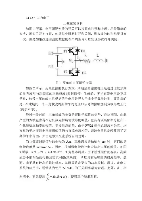
24.437 电力电子正弦脉宽调制如图1所示,电压源逆变器的开关可以按要求打开和关闭。
用最简单的方法,顶部的开关打开,如果每个周期打开和关闭,则方波的波形结果只有一次。
但是如果改进谐波的数据则在个周期内可以实现多次打开关闭。
图1 简单的电压源逆变器 如图2所示,用最直接的执行方式,所期望的输出电压是通过比较预期的参考波形与高频率的三角载波(调制信号) 生成的,无论直流电压是正还是负,信号电压的输出只根据信号电压是否大于或小于载波波形,要注意的是,在此期间一个三角载波周期的平均电压即信号的振幅加到负载形成正比(假定不变)。
经过一段时间,三角载波的负荷是正比于幅值的信号,在这期间,由此产生的方波包含有在它低频元件所需波形的幅值,也具有较高频率分量在一个载波临近频率的幅值。
需要注意的是,由于PWM 使得总谐波不失真,均方根的平均交流电压波形幅值仍与直流电压相等。
谐波分量只是转移到了更高的平率范围,并由电感式交流系统自动过滤。
当正弦波调制信号的振幅为Am ,三角载波的振幅为Ac 时,它们的调制指数就是m=Am/ Ac 。
因此,控制调制指数控制着输出电压的幅值。
如图3所示,fc/fm=21 ,t=L/R=T/3,T 为基本周期,由于感性元件的存在,高频成分不能明显的传播到交流网络(或负载),所以具有足够高的载波频率。
然而,由于具有较高的载波频率,从而导致在更多的功率损耗。
所以,在电力系统的应用中,通常认为使用2-15kHz 的开关频率最为合适。
此外,在三相系统中,建议使用)(,3N k k f f mc ∈=,使得三个波形对称。
图2 主要的脉宽调制图3 SPWM的fc/fm=48,L/R=T/3如图4所示,该过程是比较合适的,因为在该图中有三角载波,其中没有交集的载体作为信号周期。
然而,这种“超调”在一定量的范围内往往是允许获得更大的交流电压,使电压频谱呈现出差异。
需要注意的是,使用一个额外的比率形成一个反周期超过360°的对称波形。
数字电子技术基础,英语作文English: Digital electronic technology is the foundation of modern electronic devices and systems. It involves the use of digital signalsto represent and process information, enabling the creation of complex and versatile electronic devices. Understanding the basics of digital electronic technology is essential for anyone pursuing a career in electronics or related fields. This includes knowledge of binary number systems, Boolean algebra, logic gates, digital circuits, and digital signal processing. With the rapid advancement of technology, digital electronic technology continues to evolve and play a critical role in various industries such as telecommunications, computing, and consumer electronics.中文翻译: 数字电子技术是现代电子设备和系统的基础。
它涉及使用数字信号来表示和处理信息,从而实现复杂多样的电子设备的创建。
了解数字电子技术的基础知识对于任何追求电子学或相关领域职业的人来说至关重要。
优秀论文审核通过未经允许切勿外传Chapter 3 Digital Electronics3.1 IntroductionA circuit that employs a numerical signal in its operation is classified as a digital circuitputers,pocket calculators, digital instruments, and numerical control (NC) equipment are common applications of digital circuits. Practically unlimited quantities of digital information can be processed in short periods of time electronically. With operational speed of prime importance in electronics today,digital circuits are used more frequently.In this chapter, digital circuit applications are discussed.There are many types of digital circuits that electronics, including logic circuits, flip-flop circuits, counting circuits, and many others. The first sections of this unit discuss the number systems that are basic to digital circuit understanding. The remainder of the chapter introduces some of the types of digital circuits and explains Boolean algebra as it is applied to logic circuits.3.2 Digital Number SystemsThe most common number system used today is the decimal system,in which 10 digits are used for counting. The number of digits in the systemis called its base (or radix).The decimal system,therefore,the counting process. The largest digit that can be used in a specific place or location is determined by the base of the system. In the decimal system the first position to the left of the decimal point is called the units place. Any digit from 0 to 9 can be used in this place.When number values greater than 9 are used,they must be expressed with two or more places.The next position to the left of the units place in a decimal system is the tens place.The number 99 is the largest digital value that can be expressed by two places in the decimal system.Each place added to the left extends the number system by a power of 10.Any number can be expressed as a sum of weighted place values.The decimal number 2583,for example, is expressed as (2×1000)+(5×100)+(8×10)+(3×1).The decimal number system is commonly used in our daily lives. Electronically, the binary system.Electronically,the value of 0 can be associated with a low-voltage value or no voltage. The number 1 can then be associated with a voltage value larger than 0. Binary systems that use these voltage values are said to , this chapter.The two operational states of a binary system,1 and 0,are natural circuit conditions. When a circuit is turned off or the off, or 0,state. An electrical circuit that the on,or 1,state. By using transistor or ICs,it is electronically possible to change states in less than a microsecond. Electronic devices make it possible to manipulate millions of 0s and is in a second and thus to process information quickly.The basic principles of numbering used in decimal numbers apply ingeneral to binary numbers.The base of the binary system is 2,meaning that only the digits 0 and 1 are used to express place value. The first place to the left of the binary point,or starting point,represents the units,or is,location. Places to the left of the binary point are the powers of 2.Some of the place values in base 2 are 2º=1,2¹=2,2²=4,2³=8,2⁴=16,25=32,and 26=64.When bases other than 10 are used,the numbers should example.The number 100₂(read“one,zero,zero, base 2”)is equivalent to 4 in base 10,or 410.Starting with the first digit to the left of the binary point,this number this method of conversion a binary number to an equivalent decimal number,write down the binary number first. Starting at the binary point,indicate the decimal equivalent for each binary place location where a 1 is indicated. For each 0 in the binary number leave a blank space or indicate a 0 ' Add the place values and then record the decimal equivalent.The conversion of a decimal number to a binary equivalent is achieved by repetitive steps of division by the number 2.When the quotient is even with no remainder,a 0 is recorded.When the quotient process continues until the quotient is 0.The binary equivalent consists of the remainder values in the order last to first.3.2.2 Binary-coded Decimal (BCD) Number SystemWhen large numbers are indicated by binary numbers,they are difficult to use. For this reason,the Binary-Coded Decimal(BCD) method of counting was devised. In this system four binary digits are used to represent each decimal digit.To illustrate this procedure,the number 105,is converted to a BCD number.In binary numbers,To apply the BCD conversion process,the base 10 number is first divided into digits according to place values.The number 10510 gives the digits 1-0-5.Converting each displayed by this process with only 12 binary numbers. The between each group of digits is important when displaying BCD numbers.The largest digit to be displayed by any group of BCD numbers is 9.Six digits of a number-coding group are not used at all in this system.Because of this, the octal (base 8) and the binary form but usually display them in BCD,octal,or a base 8 system is 7. The place values starting at the left of the octal point are the powers of eight: 80=1,81=8,82=64,83=512,84=4096,and so on.The process of converting an octal number to a decimal number is the same as that used in the binary-to-decimal conversion process. In this method, equivalent decimal is 25810.Converting an octal number to an equivalent binary number is similar to the BCD conversion process. The octal number is first divided into digits according to place value. Each octal digit is then converted into an equivalent binary number using only three digits.Converting a decimal number to an octal number is a process of repetitive division by the number 8.After the quotient determined,the remainder is brought down as the place value.When the quotient is even with no remainder,a 0 is transferred to the place position.The number for converting 409810 to base 8 is 100028.Converting a binary number to an octal number is an importantconversion process of digital circuits. Binary numbers are first processed at a very output circuit then accepts this signal and converts it to an octal signal displayed on a readout device.must first be divided into groups of three,starting at the octal point.Each binary group is then converted into an equivalent octal number.These numbers are then combined,while remaining in their same respective places,to represent the equivalent octal number.3.2.4 Hexadecimal Number SystemThe digital systems to process large number values.The base of this system is 16,which means that the largest number used in a place is 15.Digits used by this system are the numbers 0-9 and the letters A-F. The letters A-P are used to denote the digits 10-15,respectively. The place values to the left of the .The process of changing a proper digital order.The place values,or powers of the base,are then positioned under the respective digits in step 2.In step 3,the value of each digit is recorded. The values in steps 2 and 3 are then multiplied together and added. The sum gives the decimal equivalent value of a . Initially,the converted to a binary number using four digits per group. The binary group is combined to form the equivalent binary number.The conversion of a decimal number to a ,as with other number systems. In this procedure the division is by 16 and remainders can be as large as 15.Converting a binary number to a groups of four digits,starting at the converted to a digital circuit-design applications binary signals arefar superior to those of the octal,decimal,or be processed very easily through electronic circuitry,since they can be represented by two stable states of operation. These states can be easily defined as on or off, 1 or 0,up or down,voltage or no voltage,right or left,or any other two-condition states. There must be no in-between state.The symbols used to define the operational state of a binary system are very important.In positive binary logic,the state of voltage,on,true,or a letter designation (such as A ) is used to denote the operational state 1 .No voltage,off,false,and the letter A are commonly used to denote the 0 condition. A circuit can be set to either state and will remain in that state until it is caused to change conditions.Any electronic device that can be set in one of two operational states or conditions by an outside signal is said to be bistable. Relays,lamps,switches,transistors, diodes and ICs may be used for this purpose. A bistable device .By using many of these devices,it is possible to build an electronic circuit that will make decisions based upon the applied input signals. The output of this circuit is a decision based upon the operational conditions of the input. Since the application of bistable devices in digital circuits makes logical decisions,they are commonly called binary logic circuits.If we were to draw a circuit diagram for such a system,including all the resistors,diodes,transistors and interconnections,we would face an overwhelming task, and an unnecessary one.Anyone who read the circuit diagram would in their mind group the components into standard circuits and think in terms of the" system" functions of the individual gates. Forthis reason,we design and draw digital circuit with standard logic symbols. Three basic circuits of this type are used to make simple logic decisions.These are the AND circuit, OR circuit, and the NOT circuit.Electronic circuits designed to perform logic functions are called gates.This term refers to the capability of a circuit to pass or block specific digital signals.The logic-gate symbols are shown in Fig.3-1.The small circle at the output of NOT gate indicates the inversion of the signal. Mathematically,this action is described as A=.Thus without the small circle,the rectangle would represent an amplifier (or buffer) with a gain of unity.An AND gate the 1 state simultaneously,then there will be a 1 at the output.The AND gate in Fig. 3-1 produces only a 1 out-put when A and B are both 1. Mathematically,this action is described as A·B=C. This expression shows the multiplication operation. An OR gate Fig.3-1 produces a when either or both inputs are l.Mathematically,this action is described as A+B=C. This expression shows OR addition. This gate is used to make logic decisions of whether or not a 1 appears at either input.An IF-THEN type of sentence is often used to describe the basic operation of a logic state.For example,if the inputs applied to an AND gate are all 1,then the output will be 1 .If a 1 is applied to any input of an OR gate,then the output will be 1 .If an input is applied to a NOT gate,then the output will be the opposite or inverse.The logic gate symbols in Fig. 3-1 show only the input and output connections. The actual gates,when wired into a digital circuit, would pin 14 and 7.3.4 Combination Logic GatesWhen a NOT gate is combined with an AND gate or an OR gate,it iscalled a combination logic gate. A NOT-AND gate is called a NAND gate,which is an inverted AND gate. Mathematically the operation of a NAND gate is A·B=. A combination NOT-OR ,or NOR,gate produces a negation of the OR function.Mathematically the operation of a NOR gate is A+B=.A 1 appears at the output only when A is 0 and B is 0.The logic symbols are shown in Fig. 3-3.The bar over C denotes the inversion,or negative function,of the gate.The logic gates discussed .In actual digital electronic applications,solid-state components are ordinarily used to accomplish gate functions.Boolean algebra is a special form of algebra that was designed to show the relationships of logic operations.Thin form of algebra is ideally suited for analysis and design of binary logic systems.Through the use of Boolean algebra,it is possible to write mathematical expressions that describe specific logic functions.Boolean expressions are more meaningful than complex word statements or or elaborate truth tables.The laws that apply to Boolean algebra are used to simplify complex expressions. Through this type of operation it may be possible to reduce the number of logic gates needed to achieve a specific function before the circuits are designed.In Boolean algebra the variables of an equation are assigned by letters of the alphabet.Each variable then exists in states of 1 or 0 according to its condition.The 1,or true state,is normally represented by a single letter such as A,B or C.The opposite state or condition is then described as 0,or false,and is represented by or A’.This is described as NOT A,A negated,or A complemented.Boolean algebra is somewhat different from conventional algebra withrespect to mathematical operations.The Boolean operations are expressed as follows:Multiplication:A AND B,AB,,A·BOR addition:A OR B .A+BNegation,or complementing:NOT A,,A’Assume that a digital logic circuit only C is on by itself or when A,B and C are all on expression describes the desired output. Eight (23) different combinations of A,B,and C exist in this expression because there are three,inputs. Only two of those combinations should cause a signal that will actuate the output. When a variable is not on (0),it is expressed as a negated letter. The original statement is expressed as follows: With A,B,and C on or with A off, B off, and C on ,an output (X)will occur:ABC+C=XA truth table illustrates if this expression is achieved or not.Table 3-1 shows a truth table for this equation. First,ABC is determined by multiplying the three inputs together.A 1 appears only when the A,B,and C inputs are all 1.Next the negated inputs A andB are determined.Then the products of inputs C,A,and B are listed.The next column shows the addition of ABC and C.The output of this equation shows that output 1 is produced only when C is 1 or when ABC is 1.A logic circuit to accomplish this Boolean expression is shown in Fig. 3-4.Initially the equation is analyzed to determine its primary operational function.Step1 shows the original equation.The primary function is addition,since it influences all parts of the equation in some way.Step 2 shows the primary function changed to a logic gate diagram.Step 3 showsthe branch parts of the equation expressed by logic diagram,with AND gates used to combine terms.Step 4 completes the process by connecting all inputs together.The circles at inputs,of the lower AND gate are used to achieve the negative function of these branch parts.The general rules for changing a Boolean equation into a logic circuit diagram are very similar to those outlined.Initially the original equation must be analyzed for its primary mathematical function.This is then changed into a gate diagram that is inputted by branch parts of the equation.Each branch operation is then analyzed and expressed in gate form.The process continues until all branches are completely expressed in diagram formmon inputs are then connected together.3.5 Timing and Storage ElementsDigital electronics involves a number of items that are not classified as gates.Circuits or devices of this type the operation of a system.Included in this system are such things as timing devices,storage elements,counters,decoders,memory,and registers.Truth tables symbols,operational characteristics,and applications of these items will be presented an IC chip. The internal construction of the chip cannot be effectively altered. Operation is controlled by the application of an external signal to the input. As a rule,very little work can be done to control operation other than altering the input signal.The logic circuits in Fig. 3-4 are combinational circuit because the output responds immediately to the inputs and there is no memory. When memory is a part of a logic circuit,the system is called sequential circuit because its output depends on the input plus its an input signal isapplied.A bistable multivibrator,in the strict sense,is a flip-flop. When it is turned on,it assumes a particular operational state. It does not change states until the input is altered.A flip-flop opposite polarity.Two inputs are usually needed to alter the state of a flip-flop. A variety of names are used for the inputs.These vary a great deal between different flip-flops.1. R-S flip-flopsFig.3-5 shows logic circuit construction of an R-S flip-flop. It is constructed from two NAND gates. The output of each NAND provides one of the inputs for the other NAND. R stands for the reset input and S represents the set input.The truth table and logic symbol are shown in Fig. 3-6.Notice that the truth table is somewhat more complex than that of a gate. It shows, for example,the applied input, previous output,and resulting output.To understand the operation of an R-S flip-flop,we must first look at the previous outputs.This is the status of the output before a change is applied to the input. The first four items of the previous outputs are Q=1 and =0. The second four states this case of the input to NANDS is 0 and that is 0,which implies that both inputs to NANDR are 1.By symmetry,the logic circuit will also stable with Q0 and 1.If now R momentarily becomes 0,the output of NANDR,,will rise to resulting in NANDS be realized by a 0 at S.The outputs Q and are unpredictable when the inputs R and S are 0 states.This case is not allowed.Seldom would individual gates be used to construct a flip-flop,rather than one of the special types for the flip-flop packages on a single chipwould be used by a designer.A variety of different flip-flops are used in digital electronic systems today. In general,each flip-flop type R-S-T flip-flop for example .is a triggered R-S flip-flop. It will not change states when the R and S inputs assume a value until a trigger pulse is applied. This would permit a large number of flip-flops to change states all at the same time. Fig. 3-7 shows the logic circuit construction. The truth table and logic symbol are shown in Fig. 3-8. The R and S input are thus active when the signal at the gate input (T) is 1 .Normally,such timing,or synchronizing,signals are distributed throughout a digital system by clock pulses,as shown in Fig. 3-9.The symmetrical clock signal provides two times each period.The circuit can be designed to trigger at the leading or trailing edge of the clock. The logic symbols for edge trigger flip-flops are shown in Fig.3-10.2. J-K flip-flopsAnother very important flip-flop unpredictable output state. The J and K inputs addition to this,J-K flip-flops may employ preset and preclear functions. This is used to establish sequential timing operations. Fig.3-11 shows the logic symbol and truth table of a J-K flip-flop.3. 5. 2 CountersA flip-flop be used in switching operations,and it can count pulses.A series of interconnected flip-flops is generally called a register.Each register can store one binary digit or bit of data. Several flip-flops connected form a counter. Counting is a fundamental digital electronic function.For an electronic circuit to count,a number of things must beachieved. Basically,the circuit must be supplied with some form of data or information that is suitable for processing. Typically,electrical pulses that turn on and off are applied to the input of a counter. These pulses must initiate a state change in the circuit when they are received. The circuit must also be able to recognize where it is in counting sequence at any particular time. This requires some form of memory. The counter must also be able to respond to the next number in the sequence. In digital electronic systems flip-flops are primarily used to achieve counting. This type of device is capable of changing states when a pulse is applied,output pulse.There are several types of counters used in digital circuitry today.Probably the most common of these is the binary counter.This particular counter is designed to process two-state or binary information. J-K flip-flops are commonly used in binary counters.Refer now to the single J-K flip-flop of Fig. 3-11 .In its toggle state,this flip-flop is capable of achieving counting. First,assume that the flip-flop is in its reset state. This would cause Q to be 0 and Q to be 1 .Normally,we are concerned only with Q output in counting operations. The flip-flop is now connected for operation in the toggle mode. J and K must both be made the 1 state. When a pulse is applied to the T,or clock,input,Q changes to 1.This means that with one pulse applied,a 1 is generated in the output. The flip-flop the next pulse arrives,Q resets,or changes to 0. Essentially,this means that two input pulses produce only one output pulse. This is a divide-by-two function.For binary numbers,counting is achieved by a number of divide-by-two flip-flops.To count more than one pulse,additional flip-flops must be employed. For each flip-flop added to the counter,its capacity is increased by the power of 2. With one flip-flop the maximum count was 20,or 1 .For two flip-flops it would count two places,such as 20 and 21.This would reach a count of 3 or a binary number of 11.The count would be 00,01,10,and 11. The counter would then clear and return to 00. In effect, this counts four state changes. Three flip-flops would count three places,or 20,21,and 22.This would permit a total count of eight state changes.The binary values are 000,001,010,011,100,101,110 and 111.The maximum count is seven,or 111 .Four flip-flops would count four places,or 20,21,22,and 23.The total count would make 16 state changes. The maximum count would be 15,or the binary number 1111.Each additional flip-flop would cause this to increase one binary place.河南理工大学电气工程及其自动化专业中英双语对照翻译。
附录一:外文原文Super capacitors - An OverviewKey words: Electrostatic capacitor; Electrolytic capacitor; Ceramic capacitor;Electrical double layer capacitor; Super Capacitor1.INTRODUCTIONThis paper offers a concise review on the renaissance of a conventional capacitor toelectrochemical double layer capacitor or super capacitor. Capacitors are fundamental electrical circuitelements that store electrical energy in the order of microfarads and assist in filtering. Capacitors havetwo main applications; one of which is a function to charge or discharge electricity. This function isapplied to smoothing circuits of power supplies, backup circuits of microcomputers, and timer circuitsthat make use of the periods to charge or discharge electricity. The other is a function to block the flowof DC. This function is applied to filters that extract or eliminate particular frequencies. This isindispensable to circuits where excellent frequency characteristics are required. Electrolytic capacitorsare next generation capacitors which are commercialized in full scale. They are similar to batteries in cell construction but the anode and cathode materials remain the same. They are aluminum, tantalum and ceramic capacitors where they use solid/liquid electrolytes with a separator between two symmetrical electro des.An electrochemical capacitor (EC), often called a Super capacitor or Ultra capacitor, stores electrical charge in the electric double layer at a surface-electrolyte interface, primarily in high-surface-area carbon. Because of the high surface area and the thinness of the double layer, these devices can have very a high specific and volumetric capacitance. This enables them to combine a previously unattainable capacitance density with an essentially unlimited charge/discharge cycle life. The operational voltage per cell ,limited only by the breakdown potential of the electrolyte, is usually<1 or <3 volts per cell for aqueous or organic electrolytes respectively.The concept of storing electrical energy in the electric double layer that isformed at the interface between an electrolyte and a solid has been known since the late 1800s. The first electrical device using double-layer charge storage was reported in 1957 by H.I. Becker of General Electric (U.S. Patent 2,800,616).Unfortunately, Becker’s device was imp ractical in that, similarly to a flooded battery, both electrodes needed to be immersed in a container of electrolyte, and the device was never comercialised.Becker did, however, appreciate the large capacitance values subsequently achieved by Robert A. Rightmire, a chemist at the Standard Oil Company of Ohio (SOHIO), to whom can be attributed the invention of the device in the format now commonly used. His patent (U.S. 3,288,641), filed in 1962 and awarded in late November 1966, and a follow-on patent (U.S. Patent 3,536,963) by fellow SOHIO researcher Donald L. Boos in 1970, form the basis for the many hundreds of subsequent patents and journal articles covering all aspects of EC technology.This technology has grown into an industrywith sales worth severalhundred million dollars per year. It is an in dustry that is poised today for rapid growth in the near term with the expansion of power quality needs and emerging transportation applications.Following the commercial introduction of NEC’s Super Capacitor in 1978, under licence from SOHIO, EC have evolved through several generations of designs. Initially they were used as back-up power devices for v is for cells ranging in size from small millifarad size devices with exceptional pulse power performance up to devices rated at hundreds of thousands of farads, with systems in some applications operating at up to 1,500 volts. The technology is seeing increasingly broad use, replacing batteriesolatile clock chips and complementary metal-oxide-semiconductor (CMOS) computer memories. But many other applications have emerged over the past 30 years, including portable wireless communication, enhanced power quality for distributed power generation systems, industrial actuator power sources, and high-efficiency energy storage for electric vehicles(EVs) and hybrid electric vehicles (HEVs).Overall, the unique attributes of ECs often complement the weaknesses of other power sources like batteries and fuel cells.Early ECs were generally rated at a few volts and had capacitance values measured from fractions of farads up to several farads. The trend today in some cases and in others complementing their performance.The third generation evolution is the electric double layer capacitor, where the electrical charge stored at a metal/electrolyte interface is exploited to construct astorage device. The interface can store electrical charge in the order of 610Farad. The main component in the electrode construction is activated carbon. Though this concept was initialized and industrialized some 40 years ago, there was a stagnancy in research until recent times; the need for this revival of interest arises due to the increasing demands for electrical energy storage in certain current applications like digital electronic devices, implantable medical devices and stop/start operation in vehicle traction which need very short high power pulses that could be fulfilled by electric double layer capacitors. They are complementary to batteries as they deliver high power density and low energy density. They also have longer cycle life than batteries and possess higher energy density as compared to conventional capacitors. This has led to new concepts of the so-called hybrid charge storage devices in which electrochemical capacitor is interfaced with a fuel cell or a battery. These capacitors using carbon as the main electrode material for both anode and cathode with organic and aqueous electrolytes are commercialized and used in day to-day applications. Fig.1 presents the three types of capacitors depicting the basic differences in their design and construction.Figure 1.Schematic presentation of electrostatic capacitor, electrolytic capacitor and electrical double layer capacitor.EDLCs, however suffer from low energy density. To rectify these problems, recently researchers try to incorporate transition metal oxides along with carbon in the electrode materials. When the electrode materials consist of transition metal oxides, then the electrosorption or redox processes enhance the value of specific capacitance ca. 10 -100 times depending on the nature of oxides. In such a situation, the EDLC is called as super capacitor or pseudo capacitor . This is the fourth generation capacitor. Performance of a super capacitor combines simultaneously two kinds of energy storage, i.e. non-faradic charge as in EDLC capacitors and faradaic charge similar toprocesses proceeding in batteries. The market for EC devices used for memory protection in electronic circuitry is about $150-200 million annually. New potential applications for ECs include the portable electronic device market, the power quality market, due particularly to distributed generation and low-emission hybrid cars, buses and trucks. There are some published reviews on capacitors and super capacitors . In the present overview, the evolution of electrochemical double layer capacitors starting from simple electrostatic capacitors is summarized.2. EXPERIMENTAL PARTThe invention of Leiden jar in 1745 started the capacitor technology; since then, there has been tremendous progress in this field. In the beginning, capacitors are used primarily in electrical and electronic products, but today they are used in fields ranging from industrial application to automobiles, aircraft and space, medicine, computers, games and power supply circuits. Capacitors are made from two metallic electrodes (mainly Si) placed in mutual opposition with an insulating material (dielectric) between the electrodes for accumulating an electrical charge. The basic equation relating to the capacitors is:C = εS/d (1)where C(μF) is the electrostatic capacity, the dielectric constant of the dielectric, S (cm2) the surface area of the electrode and d (cm) the thickness of the dielectric. The charge accumulating principle can be described as follows: when a battery is connected to the capacitor, flow of current induces the flow of electrons so that electrons are attracted to the positive terminal of the battery and so they flow towards the power source. As a result, an electron deficiency develops at the positive side, which becomes positively charged and an electron surplus develops at the negative side, which becomes negatively charged. This electron flow continues until the potential difference between the two electrodes becomes equal to the battery voltage. Thus the capacitor gets charged. Once the battery is removed, the electrons flow from the negative side to the side with an electron deficiency; this process leads to discharging. The conventional capacitors yield capacitance in the range of 0.1 to 1 μF with a voltage range of 50 to 400 V. Various materials such as paper (ε, 1.2-2.6), paraffin (ε 1.9-2.4), polyethylene (2.2-2.4), polystyrene (ε, 2.5-2.7), ebonite (ε, 2-3.5), polyethylene tetraphtharate (ε,3.1-3.2), water (ε, 80) sulfur(ε, 2-4.2), steatite porcelain (ε, 6-7), Al porcelain (ε, 8-10), mica(ε, 5-7)and insulated mineral oil (ε, 2.2-2.4) are used as dielectrics in capacitors.The capacitance output of these silicon based capacitors is limited and has to cope with low surface-to volume ratios of these electrodes. To increase the capacitance, as per eq., one has to increase to ∂or S and decrease; however the ∂value is largely determined by the working voltage and cannot be tampered. When aiming at high capacitance densities, it is necessary to combine the mutual benefits achieved with a high permittivity insulator material and an increased effective surface area. With Si as the substrate material, electrochemical etching produces effective surface area. The surface area of this material gets enlarged by two orders of magnitude compared to unetched surface. Electrochemically formed macroporous Si has been used for the preparation of high aspect ratio capacitors with layered SiO2/Si3N4/SiO2 insulators. Research work on the modification of conventional capacitors to increase the specific capacitance is also in progress. Approximately 30 times higher capacitance densities are reported recently for Si/Al2O3/ZnO: Al capacitor where Si is electrochemically etched porous one. Another way identified to increase the surface area of the electrodes is to form anodically formed oxides (Al, Ta); however, ceramic capacitors are based on the high dielectric constant rather than the electrode area.3. ELECTROLYTIC CAPACITORSThe next generation capacitors are the electrolytic capacitors; they are of Ta, Al and ceramic electrolytic capacitors. Electrolytic capacitors use an electrolyte as conductor between the dielectrics and an electrode. A typical aluminum electrolytic capacitor includes an anode foil and a cathode foil processed by surface enlargement and or formation treatments. Usually, the dielectric film is fabricated by anodizing high purity Al foil for high voltage applications in boric acid solutions. The thickness of the dielectric film is related to the working voltage of the aluminum electrolytic capacitor. After cutting to a specific size according to the design specification, a laminate made up of an anode foil, a cathode foil which is opposed to the dielectric film of the anode foil and a separator interposed between the anode and cathode foils, is wound to provide an element. The wound element does not have any electricalcharacteristics of electrolytic capacitor yet until completely dipped in an electrolyte for driving and housed in a metallic sheathed package in cylindrical form with a closed-end equipping a releaser. Furthermore, a sealing material made of elastic rubber is inserted into an open-end section of the sheathed package and the open-end section of the sheathed package by drawing, whereby an aluminum electrolytic capacitor is constituted. Electrolytic aluminum capacitors are mainly used as power supplies for automobiles, aircraft, space vehicles, computers, monitors, motherboards of personal computers and other electronics.There are two types of tantalum capacitors commercially available in the market; wet electrolytic capacitors which use sulfuric acid as the electrolyte and solid electrolytic capacitors which use MnO2 as the solid electrolyte. Though the capacitances derived from both Ta and Al capacitors are the same, Ta capacitors are superior to Al capacitors in temperature and frequency characteristics. For analog signal systems, Al capacitors produce a current-spike noise which does not happen in Ta capacitors. In other words, Ta capacitors are preferred for circuits which need high stability characteristics. The total world wide production of Al electrolytic capacitors amounts to US$ 3.8 billion, 99% of which are of the wet type. Unlike Ta solid electrolytic capacitors, the solid electrolyte materials used are of organic origin; polypyrrole, a functional polymer and TCNQ (7,7, 8, 8- tetracyanoquniodimethane) an organic semiconductor. Next, MnO2 solid electrolyte material is formed on the surface of that dielectric layer and on top of that a layer of polypyrrole organic solid electrolyte material is formed by electrolytic synthesis. Following this, the positive and negative electrodes are mounted to complete the electronic component. However, the capacitances of these electrolytic capacitors are in the range 0.1 to 10F with a voltage profile of 25 to 50 V.The history of development of electrolytic capacitors which were mass produced in the past as well as today is presented by S. Niwa and Y. Taketani . Many researchers try to improve the performance of these electrolytic capacitors by modifying the electrode or electrolyte. Generally, the increases in effective surface area (S) are achieved by electrolytic etching of aluminum substrate before anodization, but now it faces with the limit. It is also very difficult to decrease d because the d value is largely decided when the working voltages are decided. Increase in may be a possible routine to form composite dielectric layers by incorporating relatively large value compounds. Replacement of MnO2 by polypyrrole solid electrolyte was reported to reduce electrostatic resistance due to its higher conductivity; aromaticsulfonate ions were used as charge compensating dopant ions .A tantalum capacitor with Ta metal as anode, polypyrrole as cathode and Ta2O5 dielectric layer was also reported. In the Al solid electrolytic capacitors, polyaniline doped with inorganic and organic acids was also studied as counter electrode. In yet another work, Al solid electrolytic capacitor with etched Al foil as anode, polyaniline / polypyrrrole as cathode and Al2O3 as dielectric was developed. Ethylene carbonate based organic electrolytes and -butyrolactone based electrolytes have been tried as operating electrolytes in Al electrolytic capacitors. Masuda et al. have obtained high capacitance by electrochemically anodizing rapidly quenching Al-Ti alloy foil. Many researchers have tried the other combination of alloys such as Al-Zr, Al-Si, Al-Ti, Al-Nb and Al-Ta composite oxide films. Composite oxide films of Al2O3-(Ba0.5Sr0.5TiO3) and Al2O3- Bi4Ti3O12 on low-voltage etched aluminum foil were also studied. Nb-Ta-Al for Ta electrolytic capacitors was also tried as anode material .A ceramic capacitor is a capacitor constructed of alternating layers of metal and ceramic, with the ceramic material acting as the dielectric. Multilayer ceramic capacitors (MLCs) typically consist of ~100 alternate layers of electrode and dielectric ceramics sandwiched between two ceramic cover layers. They are fabricated by screen-printing of electrode layers on dielectric layers and co-sintering of the laminate. Conventionally, Ag-Pd is used as the electrode material and BaTiO3 is used as the dielectric ceramic. From 2000 onwards, the MLCs market has been growing in pace with the exponential development of communications. They are produced in the capacitance range of 10 F (normally the range of Ta and Al electrolytic capacitors); they are highly useful in high frequency applications. Historically, a ceramic capacitor is a two-terminal non-polar device. The classical ceramic capacitor is the disc capacitor. This device predates the transistor and was used extensively in vacuum-tube equipment (e.g radio receivers) from c. a. 1930 through the 1950s and in discrete transistor equipment from the 1950s through the 1980s. As of 2007, ceramic disc capacitors are in widespread use in electronic equipment, providing high capacity and small size at low price compared to the other types.The other ceramic materials that have been identified and used are CaZrO3, MgTiO3, SrTiO3 etc. A typical 10 F MLC is a chip of size (3.2 x 1.6 x 1.5 mm). Mn, Ca, Pd , Ag etc are some of the other internal electrodes used. Linear dielectrics and antiferroelectrics based o strontium titante have been developed for high voltage disk capacitors. These are applicable for MLCs with thinner layers because of their high coercive fields. One of the most critical material processing parameters is the degreeof homogeneous mixing of additive in the slurry. The binder distribution in the green ceramic sheet, the degree of surface roughness, fine size nickel powder, formation of green sheet, electrode deposition ad sheet stacking etc play a crucial role in the process technology. Any one of these facts if mishandled would result in the failure of the device. For instance, providing a roughess of 5 m thick green sheet to 0.5 m is mandatory so that a smooth contact surface with the inner nickel electrode can be established. This is a very important factor in avoiding the concentration of electric filed at asperities, where the charge emission from the electrode is accelerated, resulting in short failure. Conventional sheet/printing method has a technical limit of producing a thickness around 1 m dielectric; in order to decrease the thickness further, thin film technologies like CVD, sputtering, plasma-spray etc has to be used.The other types of capacitors are film capacitors which use thin polyester film and polypropylene film as dielectrics and meta-glazed capacitors which incorporate electrode plates made of film vacuum evaporated with metal such as Al. Films can be of polyester, polypropylene or polycarbonate make. Also capacitors are specified depending on the dielectric used such as polyester film capacitor, polypropylene capacitor, mica capacitor, metallized polyester film capacitor etc.4. DOUBLE LAYER CAPACITORSElectric/electrochemical double layer capacitor (EDLC) is a unique electrical storage device, which can store much more energy than conventional capacitors and offer much higher power densitythan batteries. EDLCs fill up the gap between the batteries and the conventional capacitor, allowing applications for various power and energy requirements i.e., back up power sources for electronic devices, load-leveling, engine start or acceleration for hybrid vehicles and electricity storage generated from solar or wind energy. EDLC works on the principle of double-layer capacitance at the electrode/electrolyte interface where electric charges are accumulated on the electrode surfaces and ions of opposite charge are arranged on the electrolyte side.Figure 2.Charge storage mechanism of an EDLC cell under idle and charged conditions.Fig. 2 shows the mechanism of charge storage in an EDLC cell and Fig. 3 shows the configuration of an typical EDLC cell. There are two main types of double layer capacitors as classified by the charge storage mechanism: (i) electrical double-layer capacitor; (ii) electrochemical double layer capacitor or super/pseudocapacitor. An EDLC stores energy in the double-layer at the electrode/electrolyte interface, whereas the supercapacitor sustains a Faradic reaction between the electrode and the electrolyte in a suitable potential window. Thus the electrode material used for the construction of the cell for the former is mainly carbon material while for the latter, the electrode material consist of either transition metal oxides or mixtures of carbon and metal oxides/polymers. The electrolytes can be either aqueous or non-aqueous depending on the mode of construction of EDLC cell.Figure 3.Typical configuration of an EDLC cellThere are two general directions of interest. One is the long term goal of the development of electrical propulsion for vehicles, and the other is the rapid growth of portable electronic devices that require power sources with maximum energy content and the lowest possible size and weight.5. CONCLUSIONSAccording to a market survey by Montana, super capacitors are becoming a promising solution for brake energy storage in rail vehicles. The expected technological development outside railway sector is also shown to be highly dynamic: diesel electric vehicles, catenary free operation of city light rail, starting system for diesel engines, hybrid-electric cars, industrial applications, elevators, pallet trucks etc. The time horizon expected for development is next 5 to 10 years. The main development goals will be,· long life time· increase of the rated voltage· improvements of the range of operating temperature· increase of the energy and power densitiesVery recently, hybrid car is introduced in the market but it is turned to be very expensive and out of common man’s reach. Shortage and cost of fossil fuels already instigated alternate technologies viable for traction purposes. In such a situation,EDLCs are also useful to store energy generated from non-conventional energy sources. A future possibility of service centers set up for EDLC supply similar to petrol (as on date) is not far as the main setbacks in technology development may take a decade for fruitful results.附录二:外文译文超级电容器-概述关键词:静电电容,电解电容器,陶瓷电容器,双电层 ,电容器,超级电容器1.引言本文为电化学双层电容器或超级电容器提供在一台常规电容器,简明的介绍新生的电化学双电层电容器或超级电容器。
DC Switching Power Supply Protection TechnologyAbstract: The DC switching power supply protection system, protection system design principles and machine protection measures, an analysis of switching power supply in the range of protected characteristics and its design methodology, introduced a number of practical protection circuit.Keywords: switching power supply protection circuit system designA、IntroductionDC switching regulator used in the price of more expensive high-power switching devices, the control circuit is also more complex, In addition, the load switching regulators are generally used a large number of highly integrated electronic systems installed devices. Transistors and integrated device tolerance electricity, less heat shocks. Switching Regulators therefore should take into account the protection of voltage regulators and load their own safety. Many different types of circuit protection, polarity protection, introduced here, the program protection, over-current protection, over-voltage protection, under-voltage protection and over-temperature protection circuit. Usually chosen to be some combination of protection, constitutes a complete protection system.B、Polarity protectionDC switching regulator input is generally not regulated DC power supply. Operating errors or accidents as a result of the situation will take its wrong polarity; switching power supply will be damaged. Polarity protection purposes, is to make the switching regulator only when the correct polarity is not connected to DC power supply regulator to work at. Connecting a single device can achieve power polarity protection. Since the diode D to flow through switching regulator input total current, this circuit applied in a low-power switching regulator more suitable. Power in the larger occasion,while the polarity protection circuit as a procedure to protect a link, save the power required for polarity protection diodes, power consumption will be reduced. In order to easy to operate, make it easier to identify the correct polarity or not, collect the next light.C、Procedures to protectSwitching power supply circuit is rather complicated, basically can be divided into low-power and high-power part of the control part of the switch. Switch is a high-power transistors, for the protection of the transistor switch is turned on or off power safety, we must first modulator, amplifier and other low-power control circuit. To this end, the boot to ensure the correct procedures. Switching Regulators generally take the input of a small inductor, the input filter capacitor. Moment in the boot, filter capacitor will flow a lot of surge current, the surge current can be several times more than the normal input current. Such a large surge current may contact the general power switch or relay contact melting, and the input fuse. In addition, the capacitor surge current will damage to shorten the life span of premature damage. To this end, the boot should be access to a current limiting resistor, through the current limiting resistor to capacitor charging. In order not to make the current limiting resistor excessive power consumption, thus affecting the normal switching regulator, and the transient process in the boot after a short period then automatically relays it to DC power supply directly to the switching regulator power supply. This circuit switching regulator called a "soft start" circuit.Switching regulator control circuit of the logic components required or op-amp auxiliary power supply. To this end, the auxiliary power supply must be in the switch circuit. This control circuit can be used to ensure the boot. Normal boot process is: to identify the polarity of input power, voltage protection procedures → boot → auxiliary power supply circuit and through current limiting resis tor R of the switching regulator input capacitor C →charge modulation switching regulator circuit, → short-circuit current limiting resistor stability switching regulator.In the switching regulator, the machines just because the output capacitance, and charge to the rated output voltage value of the need for a certain period of time. During this time, sampling the output amplifier with low input voltage sampling, closed-loop regulation characteristics of the system will force the switching of the transistor conduction time lengthened, so that switching transistor during this period will tend to continuous conduction, and easily damaged. To this end, the requirements of this paragraph in the boot time, the switch to switch the output modulation circuit transistor base drive signal of the pulse width modulation, can guarantee the switching transistor by the cut-off switches are becoming more and more normal state, therefore the protection of the setting up of a boot to tie in with the soft start.D、Over-current protectionWhen the load short-circuit, overload control circuit failure or unforeseen circumstances, such as would cause the flow of switching voltage regulator transistor current is too large, so that increased power tubes, fever, if there is no over-current protection device, high power switching transistor may be damaged. Therefore, the switching regulator in the over-current protection is commonly used. The most economical way is to use simple fuse. As a result of the heat capacity of small transistors, general fuse protection in general can not play a role in the rapid fuse common fuse. This method has the advantage of the protection of vulnerable, but it needs to switch transistor in accordance with specific security requirements of the work area to select the fuse specifications. This disadvantage is over-current protection measures brought about by the inconvenience of frequent replacement of fuses.Linear voltage regulator commonly used in the protection and currentlimiting to protect the cut-off in the switching regulator can be applied. However, according to the characteristics of switching regulators, the protection circuit can not directly control the output transistor switches, and over current protection must be converted to pulse output commands to control the modulator to protect the transistor switch. In order to achieve over-current protection are generally required sampling resistor in series in the circuit, this will affect the efficiency of power supply, so more for low-power switching regulator of occasions. In the high-power switching power supply, by taking into account the power consumption should be avoided as far as possible access to the sampling resistor. Therefore, there will usually be converted to over-current protection, and under-voltage protection.E、Over-voltage protectionSwitching regulator's input over-voltage protection, including over-voltage protection and output over-voltage protection. Switching regulator is not used in DC power supply voltage regulator and rectifier, such as battery voltage, if too high, so switching regulator is not working properly, or even damage to internal devices, therefore, it is necessary to use the input over-voltage protection circuit. Using transistors and relays protection circuit.In the circuit, when the input DC power supply voltage higher than the voltage regulator diode breakdown voltage value, the breakdown voltage regulator tube, a current flowing through resistor R, so that V turn-on transistor, relay, normally closed contact off open, cut off the input. Voltage regulator voltage regulator which controls the value of Vs. = Earwax-UBE. The polarity of input power with the input protection circuit can be combined with over-voltage protection, polarity protection constitute a differential circuit and over voltage protection.Output over-voltage protection switching power supply is essential. In particular, for the 5V output of the switching regulator, it is a lot of load on a high level of integration of the logic device. If at work, switching regulator sudden damage to the switch transistor, the output potential may be increased immediately to the importation of non-regulated DC power supply voltage value, causing great loss instantaneous. Commonly used method is short-circuit protection thirsted. The simplest over-voltage protection circuit. When the output voltage is too high, the regulator tube breakdown triggered thirstier turn-on, the output short-circuit, resulting in over-current through the fuse or circuit protective device to cut off the input to protect the load. This circuit is equivalent to the response time of the opening time of thirstier is about 5 ~ 10μs. The disadvantage is that its action is fixed voltage, temperature coefficient, and action points of instability. In addition, there is a voltage regulator control parameters of the discrete, model over-voltage start-up the same but has different values, difficult to debug. Esc a sudden increase in output voltage, transistors V1, V2 conduction, the thruster conduction. Reference voltage Vs. by type.F、Under-voltage protectionOutput voltage below the value to reflect the input DC power supply, switching regulator output load internal or unusual occurrence. Input DC power supply voltage drops below the specified value would result in switching regulator output voltage drops, the input current increases, not only endanger the switching transistor, but also endanger the input power. Therefore, in order to set up due to voltage protection. Due to simple voltage protection.When no voltage regulator input normal, ZD breakdown voltage regulator tube, transistors V conduction, the relay action, contact pull-in, power-switching regulator. When the input below the minimum allowable voltage value, the regulator tube ZD barrier, V cut-off, contact Kai-hop,switching regulator can not work. Internal switching regulator, as the control switch transistor circuit disorders or failure will decrease the output voltage; load short-circuit output voltage will also decline.Especially in the reversed-phase step-up or step-up switching regulator DC voltage of the protection due to over-current protection with closely related and therefore more important. Implementation of Switching Regulators in the termination of the output voltage comparators.Normally, there is no comparator output, once the voltage drops below the allowable value in the comparator on the flip, drive alarm circuit; also fed back to the switching regulator control circuit, so that switching transistor cut-off or cut off the input power.G、Over-temperature protectionSwitching regulator and the high level of integration of light-weight small volume, with its unit volume greatly increased the power density, power supply components to its work within the requirements of the ambient temperature is also a corresponding increase. Otherwise, the circuit performance will deteriorate premature component failure. Therefore, in high-power switching regulator should be set up over-temperature protection.Relays used to detect the temperature inside the power supply temperature, when the internally generated power supply overheating, the temperature of the relay on the action, so that whole circuit in a warning alarm, and the realization of the power supply over-temperature protection. Temperature relay can be placed in the vicinity of the switching transistor, the general high-power tube shell to allow the maximum temperature is 75 ℃, adjust the temperature setting to 60 ℃. When the shell after the temperature exceeds the allowable value to cut off electrical relay on the switch protection. Semiconductor switching device thermal "hot thirstier," in the over-temperature protection, played an important role. It can be used asdirected circuit temperature. Under the control of p-hot-gate thirstier (TT102) characteristics, by RT value to determine the temperature of the device turn-on, RT greater the temperature the lower the turn-on. When placed near the power switching transistor or power device, it will be able to play the role of temperature instructions. When the power control the temperature of the shell or the internal device temperature exceeds the allowed value, the heat conduction thirstier on, so that LED warning light. If the opt coupler with, would enable the whole circuit alarm action to protect the switching regulator. It can also be used as a power transistor as the over-temperature protection, crystal switch the base current by n-type gate control thirstier TT201 thermal bypass, cut-off switch to cut off the collector current to prevent overheating.I、ConclusionDiscussed above in the switching regulator of a variety of conservation, and introduces a number of specific ways to achieve. Of a given switching power supply is concerned, but also protection from the whole to consider the following points:1) The switching regulator used in the switching transistor in the DC security restrictions on the work of regional work. The transistor switches selected by the manual available transistors get DC safe working area. According to the maximum collector current to determine the input value of over-current protection. However, the instantaneous maximum value should be converted to the average current. At rated output current and output voltage conditions, the switch of the dynamic load line does not exceed a safe working area DC maximum input voltage, input over-voltage protection is the voltage value.2)The switching regulator output limit given by the technical indicators within. Work within the required temperature range, the switching regulator's output voltage, the lower limit of the output is off, due to thevoltage value of voltage protection. Over-current protection can be based on the maximum output current to determine. False alarm in order not to protect the value of a certain margin to remain appropriate.3)From the above two methods to determine the protection after the power supply device in accordance with the needs of measures to determine the alarm. Measures the general alarm sound and light alarm two police. Voice of the police applied to more complex machines, power supply parts and do not stand out in a place, it can give staff an effective warning of failure; optical Police instructions can be eye-catching and fault alarm and pointed out that the fault location and type. Protection measures should be protected as to determine the location. In the high-power, multi-channel power supply, always paying, DC circuit breakers, relays, etc. high-sensitivity auto-protection measures, to cut off the input power supply to stop working the system from damage. Through the logic control circuit to make the appropriate program cut-off switch transistor is sensitive it is convenient and economic. This eliminated large, long response time, the price of your high-power relay or circuit breaker.4) The power of putting in the protection circuit will be affected after the reliability of the system, for which want to protect the reliability of the circuit itself is higher in order to improve the reliability of the entire power system, thereby increasing its own power supply MTBF. This requires the protection of strict logic, the circuit is simple, at least components, In addition to the protection circuit should also be considered a failure of maintenance of their difficulty and their power to protect the damage.Therefore, we must be comprehensive and systematic consideration of a variety of switching power supply protection measures to ensure the normal operation of switching power supplies and high-efficiency and high reliability.直流开关稳压电源的保护技术摘要:讨论了直流开关稳压电源的保护系统,提出保护系统设计的原则和整机保护的措施,分析了开关稳压电源中的各种保护的特点及其设计方法,介绍了几种实用保护电路。
1、外文原文(复印件)A: The Utility Interface with Power Electronic SystemIntroductionWe discussed various powerline disturbances and how power electronic converters can perform as power conditioners and uninterruptible power supplies to prevent these poweline disturbances from disrupting the operation of critical loads such as computers used for controlling important processes, medical equipment, and the like. However, all power electronic converters (including those used to protect critical loads) can add to the inherent powerline disturbances by distorting the utility waveform due to harmonic currents injected into the utility grid and by producing electromagnetic interference, To illustrate the problems due to current harmonics ih in the input current i s of a power electronic load, consider the simple block diagram of Fig. 1-6A-1. Due to the finite (non-zero) internal impedance of the utility source which is simply represented by Ls in Fig. l-6A-1, the voltage waveform at the point of common coupling to the other loads will become distorted, which may cause them to malfunction. In addition to the voltage waveform distortion, some other problems due to the harmonic currents are as follows: additional heating and possibly overvoltages (due to resonance conditions) in the utility's distribution and transmission equipment, errors in metering and malfunction of utility relays, interference with communication and control signals, and so on. In addition to these problems, phase-controlled converters cause notches in the utility voltage waveform and many draw power at a very low displacement power factor which results in a very poor power factor of operation.The foregoing discussion shows that the proliferation of power electronic systems and loads has the potential for significant negative impact on the utilities themselves, as well as on their customers. One approach to minimize this impact is to filter the harmonic currents and the electromagnetic interference (EMI) produced by the power electronic loads. A better alternative, in spite of a small increase in the initial cost, may be to design the power electronic equipment such that the harmoniccurrents and the EMI are prevented or minimized from being generated in the first place. Both, the concerns about the utility interface and the design of power electronic equipment to minimize these concerns are discussed here.Generation of Current HarmonicsIn most power electronic equipment, such as switch-mode dc power supplies, uninterruptible power supplies (UPS), and ac and dc motor drives, ac-to-dc converters are used as the interface with the utility voltage source. Commonly, a line-frequency diode rectifier bridge as shown in Fig.1-6A-2 is used to convert line frequency ac into dc. The rectifier output is a dc voltage whose average magnitude Ud is uncontrolled.A large filter capacitor is used at the rectifier output to reduce the ripple in the dc voltage Ud. The dc voltage Ud and the dc current Id are unipolar and unidirectional, respectively. Therefore, the power flow is always from the utility ac input to the dc side. These line-frequency rectifiers with a falter capacitor at the dc side were discussed in detail in other section.A class of power electronic systems utilizes line-frequency thyristor-controlled ac-to-dc converters as the utility interface. In these converters, which were discussed in detail, the average dc output voltage Ud is controllable in magnitude and polarity, but the dc current Id remains unidirectional. Because of the reversible polarity of the dc voltage, the power flow through these converters is reversible. As was pointed out, the trend is to use these converters only at very high power levels, such as in high-voltage dc transmission systems. Because of the very high power levels, the techniques to ffdter the current harmonics and to improve the power factor of operation are quite different in these converters, as discussed in other section, than those for the line-frequency diode rectifiers.The diode rectifiers are used to interface with both the single-phase and the three-phase utility voltages. Typical ac current waveforms with minimal filtering were shown in other section. Typical harmonics in a single-phase input current waveform are listed in Table 1-6A-1, where the harmonic currents Ih are expressed as a ratio of the fundamental current Il. As is shown by Table 1-6A-l, such current waveformsconsist of large harmonic magnitudes. Therefore, for a finite internal per-phase source impedance Ls, the voltage distortion at the point of common coupling in Fig. 1-6A-1 can be substantial. The higher the internal source inductance Ls, the greater would be the voltage distortion.Current Harmonics and Power FactorAs we discussed in other section, the power factor PF at which an equipment operates is the product of the current ratio Il / Is and the displacement power factor DPF:In Eq. (1-6A-I), the displacement power factor equals the cosine of the angle Φ1. The current ratio Il / Is in Eq. (1-6A-l) is the ratio of the rms value of the fundamental frequency current component to the rms value of the total current. The power factor indicates how effectively the equipment draws power from the utility; at a low power factor of operation for a given voltage and power level, the current drawn by the equipment will be large, thus requiting increased volt-ampere ratings of the utility equipment such as transformers, transmission lines, and generators. The importance of the high power factor has been recognized by residential and office equipment manufacturers for their own benefit to maximize the power available from a wall outlet. For example from a 120V, 15A electrical circuit in a building, the maximum power available is 1.8 kW, provided the power factor is unity. The maximum power that can be drawn without exceeding the 15A limit decreases with decreasing power factor. The foregoing arguments indicate the responsibility and desirability on the part of the equipment manufacturers and users to design power electronic equipment with a high power factor of operation. This requires that the displacement power factor DPF should be high in Eq. (1-6A-I). Moreover, the current harmonics should be low to yield a high current ratio I1 / Is in Eq. (1-6A- 1).B: A Three-phase Pre-converter for Induction HeatingMOSFETBridge InvertersIntroductionHigh frequency power supplies, based on MOSFET bridge inverters, are already widely used for induction heating applications. These units require dc input voltages of about 400V to allow efficient operation of the MOSFETs employed. This supply voltage is usually obtained by using a three-phase rectifier stage, appropriate smoothing components or by employing thyristor phase- angle control to the mains supply. This kind of mains frequency power supply allows output power control of the induction heater, but it suffers from highly distorted input current waveforms with a low power factor. New legislation has been proposed to limit the maximum magnitude of harmonics drawn from the mains supply and different strategies have been suggested to reduce mains pollution.Investigations have been made to replace mains frequency power supplies by switched mode pre-converters. Switched mode converters can be designed to draw sinusoidal input currents thus avoiding the need for large and expensive mains frequency filters. At the same time these converters provide output power control and implementation of a small size high frequency isolation transformer. Power factor corrected three-phase ac-dc switched mode converter systems have usually been obtained using three identical single-phase converters with a common output filter. These systems overcome problems of mains pollution, but suffer from the disadvantage of a relatively large number of components and the need for complicated control and synchronization circuits. To reduce component costs, a structure based on a boost converter with three-phase input diode rectifier has been suggested. However, when operated direct-off-line from a three-phase 415V mains supply, this structure leads to high output voltages above lkV.In this paper, a novel method to achieve power factor correction for three-phase ac to dc power converters is described. The proposed topology is based on the buck converter and allows therefore output voltages to be below the maximum input voltage. The proposed topology utilizes a three- phase diode rectifier at the mains input and a single active switching device. The active switching device operates underzero-current switching conditions, resulting in very high converter efficiencies and low RFI emissions.Zero-current switching technique allows semiconductor devices to be operated at much higher switching frequencies and with reduced drive requirements compared with conventional switched mode operation.The proposed single-ended resonant converter with three-phase diode rectifier offers good opportunities for medium power, ac to dc applications. It combines simplicity and ease of control with high converter efficiency and high output power capabilities. It will be shown in the paper, that these characteristics make the converter very suitable as a direct replacement for the conventional mains frequency power supply used to supply induction heating MOSFET bridge inverters.General DescriptionA block diagram of the proposed induction heating system is shown in Fig. 1-6B-1. Block 1 represents the pre-converter that produces the dc supply voltage to feed to the RF MOSFET bridge inverter. Its output voltage should be controllable over a wide range to control the output power of the inverter and it must be able to operate with a wide range of load resistance to compensate load changes of the induction heating inverter stage. The pre-converter should operate direct-off-line from a three-phase 415V mains supply, drawing sinusoidal input current waveforms with a power factor approaching unity.Block 2 shows the RF MOSFET bridge inverter.The required maximum supply voltage of the MOSFET bridge lies between 300V and 400V. Block 3 represents the control and protection circuit used to stabilise the output power and to allow reliable operation of the induction heater in an industrial environment.Principle of Converter OperationA circuit diagram of the proposed three-phase ac to dc converter topology is shown in Fig. 1- 6B-2. The converter input currents are filtered through the input inductors L1, L2, L3. These inductors are designed so that the converter input currents are approximately constant over a whole switching cycle.During the OFF time of switch S, all three capacitors are charged by the inputcurrents I1, I2,I3. Consequently the three capacitor voltages Uc1, Uc1, Uc1 begin simultaneously to increase at a rate proportional to their respective input currents. If discontinuous operation is assumed the initial voltages of all capacitors C1, C2, C3 are zero when the switch ceases conducting. Hence, the peak voltage across each capacitor at the end of the OFF interval is proportional to their respective phase input current during the same OFF interval. Since capacitor voltages always begin at zero, it means that their average values during OFF time are linearly dependent on the phase input currents.During the ON time of switch S the energy stored in the three input capacitors C1, C2 and C3 is discharged through the six rectifier diodes VD1 –VD6, the switch S and the resonant inductor Lr. The rate of current decrease is dependent on the phase currents I1, I2, I3 and the switch current I0. The average value of the capacitor voltages Uc1, Uc2, Uc3 during the ON time are not linearly dependant on their phase input currents.To draw sinusoidal input currents from the mains supply the converter must draw input currents averaged over each switching cycle which are proportional to the phase voltages. Assuming steady state converter operation, the average phase input voltages over each switching cycle must be equal to the appropriate average input capacitor voltages during the switch OFF time plus the average input capacitor voltages during the switch ON time.Average input capacitor voltages during the switch OFF time have been shown to be proportional to the phase input currents, but during the switch ON time this is not true. However, if the switch ON time of the converter is mucteshorter than the switch OFF time, then the shape of the phase input currents will approach a sinusoidal waveform with unity power factor.2、外文资料翻译译文A:效用界面与电力电子系统介绍我们之前介绍了许多种电力线的干扰情况和电力系统转换器是如何在作为电力调节器和电力电子变换器时,用来防止那些电力线扰动干扰操作的临界荷载,例如电脑用于控制重要步骤,医疗设备,以及类似其他情况。
某钢铁企业变电所保护系统及防护系统设计1 绪论1.1 变电站继电保护的发展变电站是电力系统的重要组成部分,它直接影响整个电力系统的安全与经济运行,失恋系发电厂和用户的中间环节,起着变换和分配电能的作用,电气主接线是发电厂变电所的主要环节,电气主接线的拟定直接关系着全厂电气设备的选择、配电装置的布置、继电保护和自动装置的确定,是变电站电气部分投资大小的决定性因素。
继电保护的发展现状,电力系统的飞速发展对继电保护不断提出新的要求,电子技术、计算机技术与通信技术的飞速发展又为继电保护技术的发展不断地注入了新的活力,因此,继电保护技术得天独厚,在40余年的时间里完成了发展的4个历史阶段。
随着电力系统的高速发展和计算机技术、通信技术的进步,继电保护技术面临着进一步发展的趋势。
国内外继电保护技术发展的趋势为:计算机化,网络化,保护、控制、测量、数据通信一体化和人工智能化。
继电保护的未来发展,继电保护技术未来趋势是向计算机化,网络化,智能化,保护、控制、测量、数据通信一体化发展.微机保护技术的发展趋势:①高速数据处理芯片的应用②微机保护的网络化③保护、控制、测量、信号、数据通信一体化④继电保护的智能化1.2本文的主要工作在本次毕业设计中,我主要做了关于某钢铁企业变电所保护系统及防护系统设计,充分利用自己所学的知识,严格按照任务书的要求,围绕所要设计的主接线图的可靠性,灵活性进行研究,包括:负荷计算、主接线的选择、短路电流计算,主变压器继电保护的配置以及线路继电保护的计算与校验的研究等等。
1.3 设计概述1.3。
1 设计依据1)继电保护设计任务书.2)国标GB50062—92《电力装置的继电保护和自动装置设计规范》3)《工业企业供电》1。
3.2 设计原始资料本企业共有12个车间,承担各附属厂的设备、变压器修理和制造任务。
1、各车间用电设备情况用电设备明细见表1.1所示.表1。
1 用电设备明细表2、负荷性质本厂大部分车间为一班制,少数车间为两班或者三班制,年最大有功负荷利用小时数为。
Logic gates formed by MOS FETsAS known to us all, we don’t use the amplification characteristic of MOS FETs in digital logic circuit, and in most cases we use them as switches to control the state of the circuits. And in digital circuits we call this kind devices logic gates which act like switches. I’d like to introduce how logic gates are formed by MOS FETs in this essay.1.CMOS FETs(1)Use CMOS to form an inverterIt is shown in the picture above, two MOS FETs are placed with their gates and drains linked together. When Vin is high(the value is bigger than the turn-on voltage Vt), M1 is on with M2 off and the voltage drop between M1 is nearly 0. So Vout is approximately linked to the ground. The value of Vout is almost zero. When the input Vin is low(smaller than Vcc-Vt), M2 is on with M1 off , and the voltage drop between M2 is zero. So Vout approximately equals to Vcc.In conclusion, if the input is high, the output is low, and if the input is low, the output is high.The function of this part is a inverter.(2)Use CMOS to form a NAND gateWhen Ua and Ub are both low, Tp1 and Tp2 are on with Tn1 and Tn2 off, and the voltage drop across each of them is zrro. So the output Uy is high. When Ua is high and Ub is low, Tp1 and Tn2 is on with Tp2 and Tn1 off, and the output Uy is high. When Ua is low and Ub is high, Tp2 and Tn1 is on with Tp1 and Tn2 off, and the output Uy is high. Only when Ua and Ub are both high, the output Uy will equal low.In conclusion, these four CMOS FETs play a role of NAND gate in this case. And for an n-input NAND gate, there are n PMOS FETs parallel connected and n NMOS FETs series connected together to realize the function.(3)Use CMOS to form a NOR gateIf either of Ua and Ub is high, the NMOS connected with the input is on while the PMOS is off. So the output turns low as it is almost connected to the GND. Only in the case where both inputs are low, the NMOS FETs are off and the NMOS FETs are on, which results the output shows high.In conclusion, the output is high only when Ua and Ub are high, and otherwise it is low. An n-input NOR gate has n PMOS FETs and n NMOS FETs parallel connected.Comparing NOR gates and NAND gates, it can be found that the output voltage of a NAND gates increases when the number of its tubes increases, because the output voltage equals to the total voltage drop through all series-connected MOS FETs. Besides, when the tubes of a NOR gate becomes more, the output voltage does not change a lot because of parallel connection. The difference between NAND and NOR gates lead to the more popularity of NOR gates.(4)Use CMOS to form a XOR gateIt has similar theory with NAND gate and NOR gate. The output is high when the two inputs are different and low when two inputs are the same.(5)Working speed of CMOS logic gatesThe original switching time of MOS tube is very short. Despite the low input capacitance, the input resistance are very high, which caused the time constant τis big, so the charging and discharging time is long. The total switching time mainly depends on the τand is longer than diode and BJT switches.2.TTL(transistor-transistor logic)Theoretically, logic gates can also be made by diodes. But in reality the diodes are not ideal and there is a voltage drop when it is on (for a Si tube it’s 0.7V). So the low signals will increase by 0.7V after passing a AND gate, which also means the AND gate and OR gate made by diodes cannot be used to build a real logic circuit. To overcome this disadvantage, transistors that have inversed amplified characteristics can be applied to making a logic gate, which is also called TTL logic gates.(1)NAND gateStructure :The circuit can be divided into three parts: input stage, middle stage, output stage.Input stage: including T1, R1. The function of input stage can be regarded as a AND gate. D1 and D2 play a role of clampers, limiting the interfering pulses and protecting the transistors.Middle stage: including T2, R2, R3. As two voltage signals with inversed phase can be collected to meet the requirements of the output stage. Moreover, it can also increase the driving ability. And it play the role of amplifiers as well.Output stage: including T4, T5, D3, R4. This stage could result in a reversal in phase. In the stable state, one of T4 and T5 is always on and the other is off, which effectively decreases the power consumption and increases the ability to drive loads.Working theory:If at least one of the inputs is low, then T1 is on and in deep saturation. Apparently, T2 and T5 is on and T4 and D3 is off. So the output voltage is high.When both of the inputs are high, VT1 is in inversion and VT2 is on , VT4 and VD3 is off. VT5 is in deep saturation. So the output voltage is low.(2) Open collector gate( OC gate )The open collector gate is more flexible than ordinary TTL circuit. We could take advantage of it to realize AND logic with lines. It can also be used as a level conversion unit. In addition, open collector circuit can provide with high voltage and big current, so in normal cases LED could be driven by OC gate.3.ECL(Emitter-coupled logic)With the electron stored in the transistor limiting, the working speed can not be increased in spite of various improving measures. ECL circuits are developed to meet the higher requirements in working speed. The average delay of ECL is shorter than 2 ns, which means that ECL is the faster circuit in various digital integrated circuits.Working theoryThe core of ECL circuits is a current-controlled switching circuit. From the picture above, it is easy to see that the circuit is a differential amplifier in fact. Let Vil=-1.6, Vih=-0.8. When the input is low, VT2 will turn on in advance. Then VT1 has to turn to off. All the current will go through VT2, which is equal to the switch to the right. So the output Vo1=0V, Vo2=-0.8V. If the input is high, Vih, then VT1 turns on first. All the current will go through the left, corresponding to turning the switch to the left.Although the difference of output between high and low is the same to input, the value of output does not equal to the input. So we could not use this kind of circuits to drive different types circuits.The main features of ECL circuits are high speed and a good ability to drive a load. ECL has strong logic function and big power dissipation as well.4.I2LTo satisfy the demands of manufacturing large scale integrated circuits and increase the integration level, the circuit structure is asked to be as simple as possible and could decrease the power dissipation of unit circuit. Apparently, I2L circuit has all the characteristic above, so it’s fit to manufacture LSI.Working theory:As can be seen in the picture, it is a multi-output inverter consisting of one PNP transistor VT1 and one multi-collector NPN transistor VT2.When the input is low, the current goes through input line and results that VT2 turns off. The collector of VT2 is in open state and gives a output of high level. When the input is open, the input current forces VT2 in deep saturation, and the output is low.In conclusion, the logic shown in the picture is inverter. The main characteristics of I2L are many. It not only has a high integration level and small product of speed and power dissipation, but also possesses bad capacity of resisting disturbance, low working speed.Reference: 1.《Electronic Devices and Circuit Theory》by Robert L. Boylestad2.《Digital Fundamentals》by Thomas L. Floyd3.《Digital Logic Circuit and System Design》by Jiang LiPPing(数字逻辑电路与系统设计)4. Internet: 。
附录1 译文数字电路介绍数字电路定义:用数字信号完成对数字量进行算术运算和逻辑运算的电路称为数字电路,或数字系统。
由于它具有逻辑运算和逻辑处理功能,所以又称数字逻辑电路。
数字逻辑电路分类(按功能分):1、组合逻辑电路简称组合电路,它由最基本的的逻辑门电路组合而成。
特点是:输出值只与当时的输入值有关,即输出惟一地由当时的输入值决定。
电路没有记忆功能,输出状态随着输入状态的变化而变化,类似于电阻性电路,如加法器、译码器、编码器、数据选择器等都属于此类。
2、时序逻辑电路简称时序电路,它是由最基本的逻辑门电路加上反馈逻辑回路(输出到输入)或器件组合而成的电路,与组合电路最本质的区别在于时序电路具有记忆功能。
时序电路的特点是:输出不仅取决于当时的输入值,而且还与电路过去的状态有关。
它类似于含储能元件的电感或电容的电路,如触发器、锁存器、计数器、移位寄存器、储存器等电路都是时序电路的典型器件。
数字电路的特点:1、同时具有算术运算和逻辑运算功能数字电路是以二进制逻辑代数为数学基础,使用二进制数字信号,既能进行算术运算又能方便地进行逻辑运算(与、或、非、判断、比较、处理等),因此极其适合于运算、比较、存储、传输、控制、决策等应用。
2、实现简单,系统可靠以二进制作为基础的数字逻辑电路,简单可靠,准确性高。
3、集成度高,功能实现容易集成度高,体积小,功耗低是数字电路突出的优点之一。
电路的设计、维修、维护灵活方便,随着集成电路技术的高速发展,数字逻辑电路的集成度越来越高,集成电路块的功能随着小规模集成电路(SSI)、中规模集成电路(MSI)、大规模集成电路(LSI)、超大规模集成电路(VLSI)的发展也从元件级、器件级、部件级、板卡级上升到系统级。
电路的设计组成只需采用一些标准的集成电路块单元连接而成。
对于非标准的特殊电路还可以使用可编程序逻辑阵列电路,通过编程的方法实现任意的逻辑功能。
数字电路的应用:数字电路与数字电子技术广泛的应用于电视、雷达、通信、电子计算机、自动控制、航天等科学技术各个领域。
数制与编码(Number systems and codes) (2)数制以及数制转换 (2)二进制运算 (2)编码 (2)数字电路(Digital circuits) (2)逻辑信号与门电路 (2)逻辑电路 (2)相关参数的讨论 (3)cmos的其他输入输出结构 (3)逻辑系列 (3)组合逻辑电路(Combinational logic circuit) (3)逻辑代数 (3)组合逻辑的定义以及描述方式 (3)卡诺图化简 (4)组合逻辑器件 (4)组合逻辑分析 (4)组合逻辑设计 (4)组合逻辑要求总结 (5)时序逻辑电路(Sequential logic circuit) (5)双稳态器件和锁存器 (5)触发器 (5)基于触发器和门电路的时钟同步状态机的分析 (6)基于触发器和门电路的同步状态机设计 (6)数据检测器的设计 (6)设计方法一 (6)设计方法二 (7)注意 (7)关于计数器的讨论(counter) (7)计数器的一些基本概念 (7)基于74163的设计和分析 (8)要清楚如下内容: (8)利用74163实现其他的二进制计数器 (8)利用74163实现其他计数方式的计数器 (8)利用74163实现序列信号发生器(sequence generators) (8)关于移位寄存器的讨论(shift-registers) (9)移位寄存器的一些基本概念 (9)基于7494的设计和分析 (9)利用194实现串行数据检测 (9)反馈移位寄存器计数器 (9)信号发生器的设计 (9)设计方法一:计数器+组合逻辑 (10)设计方法二:移位寄存器+反馈函数 (10)设计方法三:反馈移位寄存器计数器+组合逻辑 (10)存储器 (10)ROM (10)RAM (10)数制与编码(Number systems and codes)本部分包括的内容包括如下:数制以及数制转换(number system and general positional-number-systemconversions)a.、什么是按位计数制(positional-number-system);b、什么是二进制(binary)、八进制(octal)、十六进制(hexadecimal)和十进制(decimal),以及他们的表示方法;c、以上四种按位计数制之间的相互转换(conversions);二进制运算,包括无符号的二进制运算和有符号的二进制运算(addition and subtractionof unsigned binary numbers and negative numbers)a、无符号二进制运算的基本原则:逢二进一(addition)和借一当二(subtraction);b、无符号二进制运算:乘法(Multiplication)和除法(Division)c、原、补、反码(signed-magnitude, 2’-complement, 1’-complement)——负数表式(the representation of negative numbers)的方法——如何构建原补反三码以及他们之间的相互转换;d、补码的加法法则(addition rules)和减法法则(subtraction rules)——带符号的二进制加减;e、溢出(overflow)判定;编码(coding)a、格雷码(gray code)b、8421码(8421BCD code)c、余三码(excess-3 code)——余三码是BCD码d、2421——BCDe、error-detecting codes(even-parity code & odd-parity code)f、其他编码形式;数字电路(Digital circuits)本部分内容包括如下:逻辑信号与门电路(logic signals and gates)——各种门的符号以及逻辑原理逻辑电路(logic circuit)a、cmos和三极管(transistors)的理想开关模型;b、cmos非门电路(cmos inverter circuit);c、其他cmos门电路的构建——三个原则:nmos和pmos互补(complement),nmos串联则pmos并联,nmos并联则pmos串联——nmos串联构成与操作,nmos并联构成或操作——输出带非(inversion)号(如果实现不带非号输出的逻辑,则需先设计带非号的逻辑输出,然后再级联一个基本反相器basic cmos invertercircuit);相关参数的讨论——多数参数都要分别讨论高低电平下的情况a、正逻辑(positive logic)和负逻辑(negative logice)b、逻辑电平(logic levels)的定义;c、噪声容限(noise margins);d、阻性负载(resistive loads)下的讨论:扇入(fan-in)、扇出(fan-out)以及灌电流(sinking current)和提供电流(sourcing current)的基本概念;e、非理想输入(nonideal inputs)下的讨论:负载效应(effects of loading)和未用输入端(unused inputs)的处理;f、容性负载(capacitive loads)下的讨论:转换时间(transition time)和传播延迟(propagation dely);g、功率(power)cmos的其他输入输出结构(other cmos input and output structuers)——工作原理以及符号;a、输入结构:施密特触发输入(schmitt-trigger input);b、输出结构:传输门(transmission gates)、三态输出(three-state outputs:H(1). L(0). Hi-Z)、漏极开路输出(open-drain outputs:OD gates)逻辑系列(logic family)组合逻辑电路(Combinational logic circuit)逻辑代数(logic algebra, boolean algebra, duality algebra)a、逻辑代数的基本公理(axioms)和定理(theorems)b、利用逻辑代数化简——主要利用吸收定理(covering theorem)和一致率(consensus theorem);c、对偶性原理(principle of duality)(正逻辑与负逻辑之间时对偶关系)以及广义德摩根定理(generalized DeMorgan’s theorem)的应用——主要用来求非函数;d、香农定理(shannon’s expansion theorems);e、与或(AND-OR)逻辑变成与非与非逻辑(NAND-NAND)以及或与(NOR-AND)逻辑变成或非或非逻辑(NOR-NOR)的代数方法;组合逻辑的定义以及描述方式——给定逻辑,可以用下面的方式表达出来a、真值表(truth table)b、卡诺图(Karnaugh-map)c、逻辑表达式(logic expression, logic function)d、定时图(timing diagrams)e、逻辑图(logic diagrams)f、逻辑描述(logic description)卡诺图化简(minimization of logic function using k-maps)a、逻辑函数的标准型(standard representations)与真值表(truth tables)和卡诺图(k-maps)之间的关系:最小项(minterm)、最大项(maxterm)、最小项列表(minterm list)、最大项列表(maxterm list)、和之积(product of sums expression, or-and)、积之和(sum of products expression, and-or)、标准项(normal term)的概念以及它们和真值表,卡诺图之间的关系;b、构架卡诺图c、利用卡诺图实现最小和(minimizing sums of products):圈1圈;d、利用卡诺图实现最小积(minimizing products of sums):圈0圈;e、一些基本概念在卡诺图化简中的应用以及主蕴含项定理(prime-implicant theorem):隐含关系(imply),蕴含项(implicant),主蕴含项(prime-implicant),质主蕴含项(essential prime implicants),次质主蕴含项(secondary essential prime implicant),奇异1单元(distinguished 1-cell);f、带无关输入(don’t care)组合的逻辑函数的卡诺图化简;组合逻辑器件——功能描述,引脚定义,真值表(功能表)a、与(and)、或(or) 、非(not) 基本门以及与非(nand)或非(nor)等复合逻辑门;b、异或门(xor)以及异或非门(xnor)——实现等值比较或者奇偶性判定的电路;c、三态门(three-state gates)电路以及分时总线(bus)的实现d、二进制译码器(binary decoders):’139和‘138e、二进制编码(binary encoders)以及优先编码(priority encoders)原理:‘148f、多路复用器(multiplexer):‘151g、数值比较器(magnitude comparators):‘85h、加法器(full adders)以及先行进位(carry-lookahead adders)概念:‘283组合逻辑分析(combinational-circuit analysis)a、基于门电路的组合逻辑分析:电路图(logic diagram)——真值表——逻辑表达式(logic expression)——定时图(timing diagram)——逻辑描述(logic description)等b、静态冒险(static hazard)分析与消除:静态1冒险(static 1 hazard)和0冒险(0 hazard),卡诺图判断冒险以及消除冒险c、基于组合逻辑功能器件的分析:依据各个器件的逻辑输出去判定电路的逻辑功能;组合逻辑设计(combinational-circuit design)a、圈到圈设计(bubble-to-bubble logic design)b、基于门电路的设计——最小成本设计(minimum cost design):逻辑抽象(logic abstraction)——真值表——卡诺图化简——表达式输出——电路图;c、基于门电路的设计——最小风险设(minimum hazard design)计:逻辑抽象——真值表——卡诺图化简(化简同时考虑到定时冒险的因素)——逻辑表达式——电路图;d、利用译码器实现组合逻辑:标准译码器芯片(输出低电平有效)的每个输出都对应着一个最小项的非或者最大项。
中英文对照资料外文翻译文献外文文献:Designing Stable Control LoopsThe objective of this topic is to provide the designer with a practical review of loop compensation techniques applied to switching power supply feedback control. A top-down system approach is taken starting with basic feedback control concepts and leading to step-by-step design procedures, initially applied to a simple buck regulator and then expanded to other topologies and control algorithms. Sample designs are demonstrated with Math cad simulations to illustrate gain and phase margins and their impact on performance analysis.I. I NTRODUCTIONInsuring stability of a proposed power supply solution is often one of the more challenging aspects of the design process. Nothing is more disconcerting than to have your lovingly crafted breadboard break into wild oscillations just as its being demonstrated to the boss or customer, but insuring against this unfortunate event takes some analysis which many designers view as formidable. Paths taken by design engineers often emphasize either cut-and-try empirical testing in the laboratory or computer simulations looking for numerical solutions based on complex mathematical models. While both of these approach a basic understanding of feedback theory will usually allow the definition of an acceptable compensation network with a minimum of computational effort.II. S TABILITY D EFINEDFig. 1. Definition of stabilityFig. 1 gives a quick illustration of at least one definition of stability. In its simplest terms, a system is stable if, when subjected to a perturbation from some source, its response to that perturbation eventually dies out. Note that in any practical system, instability cannot result in a completely unbounded response as the system will either reach a saturation level –or fail. Oscillation in a switching regulator can, at most, vary the duty cycle between zero and 100% and while that may not prevent failure, it wills ultimate limit the response of an unstable system. Another way of visualizing stability is shown in Fig. 2. While this graphically illustrates the concept of system stability, it also points out that we must make a further distinction between large-signal and small-signal stability. While small-signal stability is an important and necessary criterion, a system could satisfy thisrt quirement and yet still become unstable with a large-signal perturbation. It is important that designers remember that all the gain and phase calculations we might perform are only to insure small-signal stability. These calculations are based upon – and only applicable to – linear systems, and a switching regulator is – by definition –a non-linear system. We solve this conundrum by performing our analysis using small-signal perturbations around a large-signal operating point, a distinction which will be further clarified in our design procedure discussion。
优秀论文审核通过
未经允许切勿外传
原文:
Digital circuit definition:
Completes with the digital signal to the digital quantity carries onthe arithmetic operation and the logic operation electric circuit iscalled the digital circuit, or number system. Because it and the logical processing function, therefore calls thenumeral logic circuit.
Numeral logic circuit classification (according to function minute): 1st, combinatory logic electric circuit
The abbreviation combination circuit, it becomes by the mostbasic logical gate electric circuit combination. The characteristicis: Output value only and then input value related, namely output onlyby then input value decision. The electric circuit , the output condition changes along with the inputcondition change, is similar to the resistance electric circuit, likethe accumulator, the decoder, the encoder, the data selector and so onall belong to this kind.
2nd, succession logic circuit
The abbreviation sequence circuit, it is adds on the feedbacklogic return route by the most basic logical gate electric circuit (tooutput the electric circuit which input) or the component combinationbecomes, lies in the sequence circuit with the combination circuitessence difference to . The sequence circuitcharacteristic is: The output not only was decided by then inputvalue, moreover also the and circuit past condition concerned. It issimilar to containing the stored energy part the inductance or theelectric capacity electric circuit, like electric circuit and so ontrigger, latch, counter, shift register, reservoir all is the sequencecircuit typical component.
Digital circuit characteristic:
1st, simultaneously and the logicoperation function
The digital circuit is take the binary system logic algebra asmathematics foundation, the use binary numeral signal, both can carryon the arithmetic operation and to be able conveniently to carry onthe logic operation (with, or, non-, judgement, comparison, processingand so on), therefore extremely suits to application and so onoperation, comparison, memory, transmission, control, decision-making.
2nd, realization simple, the system is reliable
By binary system underlie numeral logic circuit, simplereliable, the accuracy is rate realization is easy
Integration rate ,service, maintenance nimble convenient, along with the integratedcircuit technology rate is more and more along with small scale integration electric circuit (SSI),center scale integrated circuit (MSI), large scale integrated circuit(LSI), ultra large scale integrated circuit (VLSI) the developmentalso from the part level, the component level, the part level, theboard card level rises to the system level. The electric circuitdesign composition only must use some standards the integrated circuitblock unit connection to become. Also may use the programmableforeword logic array electric circuit regarding the non- standardspecial electric circuit, through programming method realization freelogic function.
Digital circuit application:
Digital circuit and numeral electronic technology widespreadapplication to science and technology each domain and so ontelevision, radar, correspondence, electronic accounting machine,automatic control, astronautics.
数字电路定义:
用数字信号完成对数字量进行算术运算和逻辑运算的电路称为数字电路,或数字系统。
由于它具有逻辑运算和逻辑处理功能,所以又称数字逻辑电路。
数字逻辑电路分类(按功能分):
1、组合逻辑电路
简称组合电路,它由最基本的的逻辑门电路组合而成。
特点是:输出值只与当时的输入值有关,即输出惟一地由当时的输入值决定。
电路没有记忆功能,输出状态随着输入状态的变化而变化,类似于电阻性电路,如加法器、译码器、编码器、数据选择器等都属于此类。
2、时序逻辑电路
简称时序电路,它是由最基本的逻辑门电路加上反馈逻辑回路(输出到输入)或器件组合而成的电路,与组合电路最本质的区别在于时序电路具有记忆功能。
时序电路的特点是:输出不仅取决于当时的输入值,而且还与电路过去的状态有关。
它类似于含储能元件的电感或电容的电路,如触发器、锁存器、计数器、移位寄存器、储存器等电路都是时序电路的典型器件。
数字电路的特点:
1、同时具有算术运算和逻辑运算功能
数字电路是以二进制逻辑代数为数学基础,使用二进制数字信号,既能进行算术运算又能方便地进行逻辑运算(与、或、非、判断、比较、处理等),因此极其适合于运算、比较、存储、传输、控制、决策等应用。
2、实现简单,系统可靠
以二进制作为基础的数字逻辑电路,简单可靠,准确性高。
3、集成度高,功能实现容易
集成度高,体积小,功耗低是数字电路突出的优点之一。
电路的设计、维修、维护灵活方便,随着集成电路技术的高速发展,数字逻辑电路的集成度越来越高,集成电路块的功能随着小规模集成电路(SSI)、中规模集成
电路(MSI)、大规模集成电路(LSI)、超大规模集成电路(VLSI)的发展也从元件级、器件级、部件级、板卡级上升到系统级。
电路的设计组成只需采用一些标准的集成电路块单元连接而成。
对于非标准的特殊电路还可以使用可编程序逻辑阵列电路,通过编程的方法实现任意的逻辑功能。
数字电路的应用:
数字电路与数字电子技术广泛的应用于电视、雷达、通信、电子计算机、自动控制、航天等科学技术各个领域。