TDA9116中文资料
- 格式:pdf
- 大小:744.60 KB
- 文档页数:47

AD9516_3----集成的2.0 GHz VCO的14路输出时钟发生器一、特征:①低相位噪声,锁相环(PLL)②片上VCO从1.75 GHz到2.25 GHz调谐③外部可选的VCO / VCXO 高达2.4 GHz④1个差分或2个单端参考输入⑤接受LVPECL ,LVDS或CMOS 250 MHz的输出频率⑥6双1.6 GHz的LVPECL输出,每对输出共享1到32位分频器与粗相位延迟⑦4对为800 MHz LVDS时钟输出,每对输出共用两个级联的粗相位延迟1到32的分频器⑧上电时所有输出自动同步可用手动输出同步64引脚LFCSP二、介绍:AD9516 -31集成了片上PLL和VCO,提供了多输出时钟分配功能,具有亚皮秒级的抖动性能。
片上VCO从1.75 GHz到2.25 GHz调谐,芯片外部可以使用高达2.4 GHz的VCO / VCXO 。
AD9516- 3侧重于低抖动和相位噪声数据转换器的性能最大化问题,可以应用于对抖动和相位噪声要求很高的问题上。
三、应用①低抖动,低相位噪声时钟分配②10/40/100 Gb /秒的网络线卡,包括SONET③同步以太网,OTU2/3/4④前向纠错(G.710 )⑤高速时钟的ADCs, DACs, DDSs, DDCs, DUCs, MxFEs⑥高性能无线收发器⑦自动测试设备(ATE)和高性能仪器仪表四、芯片的规格(1)供应的电源:Vs=Vs_LVPECL=3.3 V ± 5%;Vs≤ Vcp≤ 5.25 V; Ta= 25°C; RSET = 4.12 kΩ; CPRSET = 5.1 kΩ四、原理框图AD9516-3具有6个LVPECL输出(三对),4个LVDS输出(两对)。
每个LVDS输出可配置为两个CMOS输出,LVPECL输出工作频率为1.6 GHz ,LVDS输出工作频率为800 MHz,CMOS输出工作频率为250 MHz。
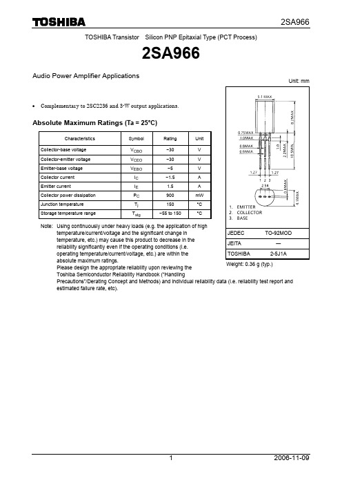
TOSHIBA Transistor Silicon PNP Epitaxial Type (PCT Process)2SA966Audio Power Amplifier Applications• Complementary to 2SC2236 and 3-W output applications.Absolute Maximum Ratings (Ta = 25°C)Characteristics Symbol Rating UnitCollector-base voltage V CBO −30 V Collector-emitter voltage V CEO −30 V Emitter-base voltage V EBO −5 V Collector current I C−1.5 AEmitter currentI E 1.5 A Collector power dissipation P C 900 mW Junction temperature T j 150 °C Storage temperature rangeT stg−55 to 150°CNote: Using continuously under heavy loads (e.g. the application of high temperature/current/voltage and the significant change in temperature, etc.) may cause this product to decrease in thereliability significantly even if the operating conditions (i.e. operating temperature/current/voltage, etc.) are within the absolute maximum ratings.Please design the appropriate reliability upon reviewing the Toshiba Semiconductor Reliability Handbook (“HandlingPrecautions”/Derating Concept and Methods) and individual reliability data (i.e. reliability test report and estimated failure rate, etc).Unit: mmJEDEC TO-92MOD JEITA ―TOSHIBA 2-5J1A Weight: 0.36 g (typ.)Electrical Characteristics (Ta = 25°C)Characteristics Symbol TestCondition MinTyp.Max UnitCollector cut-off current I CBO V CB = −30 V, I E = 0 ――−100nAEmitter cut-off current I EBO V EB = −5 V, I C = 0 ――−100nA Collector-emitter breakdown voltage V (BR) CEO I C = −10 mA, I B = 0 −30 ―― V Emitter-base breakdown voltage V (BR) EBO I E = −1 mA, I C = 0 −5 ―― VDC current gain h FE(Note)V CE = −2 V, I C = −500 mA 100 ― 320Collector-emitter saturation voltage V CE (sat)I C = −1.5 A, I B = −0.03 A ――−2.0V Base-emitter voltage V BE V CE = −2 V, I C = −500 mA ――−1.0V Transition frequency f T V CE = −2 V, I C = −500 mA ― 120 ― MHz Collector output capacitance C ob V CB = −10 V, I E = 0, f = 1 MHz ― 40 ― pF Note: h FE classification O: 100 to 200, Y: 160 to 320Markinglead (Pb)-free package orlead (Pb)-free finish.indicatorCollector current I C (mA)h FE – ICD C c u r re n t g a i n h F ECollector current I C (mA)V CE (sat) – I CC o l l e c t o r -e m i t t e r s a t u r a t i on v o l t a g eV C E (s a t ) (V )Base-emitter voltage V BE (V)I C – V BEC oll e c t o rc u r r e n t I C (m A )Ambient temperature Ta (°C)P C – TaC o l l e c t o r p owe r d i s s ip a t io n P C (W )Collector-emitter voltage V CE (V)Safe Operating AreaC o l l e c t o r c u r r e n t I C (A )1.00 0 20 40 60 80 100 120 140 160 1800.20.40.60.8−−−−−−−−−−−−−−−−−−Collector-emitter voltage V CE (V)I C – V CEC o l l e c t o r c u r r e n t I C (m A )−−−−−−−−−−−−−−−−−RESTRICTIONS ON PRODUCT USE20070701-EN •The information contained herein is subject to change without notice.•TOSHIBA is continually working to improve the quality and reliability of its products. Nevertheless, semiconductor devices in general can malfunction or fail due to their inherent electrical sensitivity and vulnerability to physical stress. It is the responsibility of the buyer, when utilizing TOSHIBA products, to comply with the standards of safety in making a safe design for the entire system, and to avoid situations in which a malfunction or failure of such TOSHIBA products could cause loss of human life, bodily injury or damage to property.In developing your designs, please ensure that TOSHIBA products are used within specified operating ranges as set forth in the most recent TOSHIBA products specifications. Also, please keep in mind the precautions and conditions set forth in the “Handling Guide for Semiconductor Devices,” or “TOSHIBA Semiconductor Reliability Handbook” etc.• The TOSHIBA products listed in this document are intended for usage in general electronics applications (computer, personal equipment, office equipment, measuring equipment, industrial robotics, domestic appliances, etc.).These TOSHIBA products are neither intended nor warranted for usage in equipment that requires extraordinarily high quality and/or reliability or a malfunction or failure of which may cause loss of human life or bodily injury (“Unintended Usage”). Unintended Usage include atomic energy control instruments, airplane or spaceship instruments, transportation instruments, traffic signal instruments, combustion control instruments, medical instruments, all types of safety devices, etc.. Unintended Usage of TOSHIBA products listed in his document shall be made at the customer’s own risk.•The products described in this document shall not be used or embedded to any downstream products of which manufacture, use and/or sale are prohibited under any applicable laws and regulations.• The information contained herein is presented only as a guide for the applications of our products. No responsibility is assumed by TOSHIBA for any infringements of patents or other rights of the third parties which may result from its use. No license is granted by implication or otherwise under any patents or other rights of TOSHIBA or the third parties.• Please contact your sales representative for product-by-product details in this document regarding RoHS compatibility. Please use these products in this document in compliance with all applicable laws and regulations that regulate the inclusion or use of controlled substances. Toshiba assumes no liability for damage or losses occurring as a result of noncompliance with applicable laws and regulations.。


Number Name Description1 GATE HS Gate drive output for the N-Channel High side MOSFET2 BOOT Floating bootstrap pin. To beconnected to the external bootstrapcapacitor to generate the gate drive voltage for the high side N-ChannelMOSFET 3 PWM Input for the PWM controller signal 4 GND Ground 5 GATE LS Gate drive output for the N-Channel Low Side MOSFET 6 VCC Supply voltage 7 PVCC Input to adjust the High Side gatedrive8 PHASE To be connected to the junction ofthe High Side and the Low Side MOSFET • Fast rise and fall times for frequencies up to 2 MHz• Capable of sinking more than 4A peak currents for lowest switching losses• Charges High Side MOSFET gate drive voltage from 6 to 12V according to PVCC setting; Low Side MOSFET at 12 V.• Adjustable High Side MOSFET gate drive voltage via PVCC pin for optimizing ON losses and gate drive losses• Integrates the bootstrap diode for reducing the part count• Prevents from cross-conducting by adaptive gate drive control • High voltage rating on Phase node• Supports shut-down mode for very low quiescent current through three-state input • Compatible to standard PWM controller ICs (Intersil, Analog Devices) • Floating High Side MOSFET drive• Footprint compatible to TDA21101G and HIP6601B• Ideal for multi-phase Desktop CPU supplies on motherboards and VRM´sType Package Marking Ordering Code TDA21106 P-DSO-8 21106 Q67042-S4223GATE PHASE2 7 P VCC3 6 V CCGND GATE LSP-DSO-8High speed Driver with bootstrapping for dual Power MOSFETsFeaturesPinoutGeneral DescriptionThe dual high speed driver is designed to drive a wide range of N-Channel low side and N-Channel high side MOSFETs with varying gate charges. It has a small propagation delay from input to output, short rise and fall times and the same pin configuration to be compatible to TDA21101G and HIP6601B. In addition it provides protection features as well as a three-state mode for efficiency reasons. The high breakdown voltage makes it suitable for mobile applications.Target applicationThe dual high speed driver is designed to work well in half-bridge type circuits where dual N-Channel MOSFETs are utilized. A circuit designer can fully take advantage of the driver´s capabilities in high-efficiency, high-density synchronous DC/DC converters that operate at high switching frequencies, e.g. in multi-phase convertersfor CPU supplies on motherboards and VRM´s but also in motor drive and class-D amplifier type applications.Absolute Maximum RatingsAt Tj = 25 °C, unless otherwise specifiedValue Parameter SymbolMin. Max.UnitVoltage supplied to ‘VCC’ pin; DC V VCC -0.3 25 Voltage supplied to ‘PVCC’ pin; DC V PVCC -0.3 25 Voltage supplied to ‘PWM’ pin V PWM -0.3 5,5 Voltage supplied to ‘BOOT’ pin referenced to ‘PHASE’ V BOOT –V PHASE-0,3 25 Voltage supplied to ‘BOOT’ pin referenced to ‘GND’ V BOOT-0,3 45 Voltage rating at ‘PHASE’ pin, DC V PHASE -1 25 Voltage rating at ‘PHASE’ pin, t pulse_max = 500nsMax Duty Cycle = 2%V PHASE -20 30Voltage supplied to GATE HS pin referenced to ‘PHASE’ T pulse_max < 100ns, E nergy < 2uJ V GATEHS -3.5 V BOOT+0.3Voltage supplied to GATE LS pin referenced to ‘GND’ T pulse_max < 100ns, E nergy < 2uJ V GATELS -5 V VCC+0.3VJunction temperature T J -25 150 Storage temperature T S -55 150°C ESD Rating; Human Body Model 4 KV IEC climatic category; DIN EN 60068-1 55/150/56 -Thermal CharacteristicValuesParameter SymbolMin.Typ. Max.UnitThermal resistance, junction-soldering point 95Thermal resistance, junction-ambient 125K/WOperating ConditionsAt Tj = 25 °C, unless otherwise specifiedValuesParameter Symbol ConditionsMin.Typ. Max.UnitVoltage supplied to‘VCC’ pinsV VCC10.813.2VVoltage supplied to ‘PVCC’ pins V PVCC 613.2VInput signal transitionfrequencyf 0.1 2 MHzPower dissipation P TOT T A = 25 °C, T J = 125 °C 0.8 W Junction temperature T J-25 150 °C Electrical CharacteristicAt Tj = 25 °C, unless otherwise specifiedValues Parameter SymbolConditionsMin. Typ. Max.UnitSupply CharacteristicQuiescent current I PVCC+I VCCQ 1.8 V ≤ V PWM≤ 3.0 V 1,3. 3 VCC supply current I VCC f =1 MHz,V PVCC = V VCC = 12 VNo load5 8 PVCC supply current I PVCC f =1 MHz,V PVCC = V VCC = 12 VNo load 6 8.5mAUnder-voltagelockoutV VCC rising threshold 9.7 10.1 10.5Under-voltage lockout V VCC fallingthreshold 7.3 7.6 8.0VInput CharacteristicCurrent in ‘PWM’ pin I PWM_L V_PWM = 0.4 V -80 -115 -150 Current in ‘PWM’ pin I PWM_H V_PWM = 4.5 V 120 180 250µAShut down window V IN_SHUT t_SHUT > 300 ns 1.7 3.1 V Shut down hold-offtimet_SHUT 1.6 V ≤ V PWM≤ 3.2 V100 190 300 ns PWM pin open V PWM_O 1.8 2.0 2.2 PWM Low level V PWM_L 1.4 PWM High level V PWM_H 3.7 VPulse width High Side t_P= Pulse width on PWMpin40 nsAt Tj = 25 °C, unless otherwise specifiedDynamic CharacteristicTurn-on propagation Delay High Side t d(ON)_HS 20 35 Turn-off propagation delay High Side t d(OFF)_HS 1525Rise time High Side t r_HS 20 33 Fall time High Side t f_HS 15 25 Turn-on propagation Delay Low Sidet d(ON)_LS 15 27 Turn-off propagation delay Low Sidet d(OFF)_LS 10 20 Rise time Low Side t r_LS 20 33Fall time Low Side t f_LSP PVCC = V VCC = 12 V C ISS = 3000 pF 15 25 nsAt Tj = 125 °C, unless otherwise specifiedDynamic CharacteristicTurn-on propagation Delay High Side t d(ON)_HS 25 Turn-off propagation delay High Sidet d(OFF)_HS18Rise time High Side t r_HS24 Fall time High Side t f_HS 22 Turn-on propagation Delay Low Sidet d(ON)_LS 18 Turn-off propagation delay Low Sidet d(OFF)_LS15 Rise time Low Side t r_LS 21 Fall time Low Side t f_LSP PVCC = V VCC = 12 V C ISS = 3000 pF19nsTiming diagramAt Tj = 25 °C, unless otherwise specifiedValuesParameter Conditions Min.Typ. Max.Unit Output Characteristic High Side (HS) and Low Side (LS), ensured by design HS; Source V PVCC = V VCC = 12 V I _HS_SRC = 2 A 1 (1)ΩHS; Sink V PVCC = V VCC = 12 V 0.9 1.3 Ω LS; Source V PVCC = V VCC = 12 V I _HS_SRC = 2 A 1.4 (2)ΩOutput Resistance LS; Sink V PVCC = V VCC = 12 V 0.9 1.3 ΩHS; Source 4HS; Sink 4LS; Source 4Peak output-current LS; Sink V PVCC = V VCC = 12 V t_P_HS / Pulse < 20 ns t_P_LS / Pulse < 40 ns 4A 1Incremental resistance V BOOT -V GATEHS =4.3V @ I SOURCE =2A 2Incremental resistance V VCC –V GATELS =4.4V @ I SOURCE =2A1 V ~5V1 Vt f LSt r LSPackage Drawing P-DSO-8-3Footprint Drawing P-DSO-8-3e A L B1,27 mm 5,69 mm 1,31 mm 0,65 mmPublished byInfineon Technologies AG,Bereichs KommunikationSt.-Martin-Strasse 53,D-81541 MünchenInfineon Technologies AG 1999All Rights Reserved.Attention please!The information herein is given to describe certain components and shall not be considered as warranted characteristics.Terms of delivery and rights to technical change reserved.We hereby disclaim any and all warranties, including but not limited to warranties of non-infringement, regarding circuits, descriptions and charts stated herein.Infineon Technologies is an approved CECC manufacturer.InformationFor further information on technology, delivery terms and conditions and prices please contact your nearest Infineon Technologies Office in Germany or our Infineon Technologies Representatives worldwide (see address list).WarningsDue to technical requirements components may contain dangerous substances.For information on the types in question please contact your nearest Infineon Technologies Office. Infineon Technologies Components may only be used in life-support devices or systems with the express written approval of Infineon Technologies, if a failure of such components can reasonably be expected to cause the failure of that life-support device or system, or to affect the safety or effectiveness of that device or system Life support devices or systems are intended to be implanted in the human body, or to support and/or maintain and sustain and/or protect human life. If they fail, it is reasonable to assume that the health of the user or other persons may be endangered.。

LM5116宽范围同步降压控制器概述该LM5116是一个同步降压控制器,适用于高输入电压或宽输入电压的环境中。
其控制方式是电流模式控制,该控制方式是利用一个模拟出来的电流斜坡。
电流模式控制提供了固有的线路前馈,以周期电流限制和易于循环的环路补偿。
电流模式控制提供固有的线性前馈,周期性循环的电流限制以及环路补偿。
仿真控制斜坡的使用可以减少脉宽调制电路的噪声灵敏度,是高输入电压应用中实现小占空比的可靠控制所必需的。
其工作频率可编程,从50kHz 至1MHz。
LM5116是驱动外部高边和低边的NMOS电源开关,这两个MOS管有自适应的死区时间控制。
可由用户选择二极管仿真的模式使芯片在轻负载时能够提高不连续工作模式的效率。
低静态关断电流就能使芯片不工作,并消耗总输入电流中的10μA。
其它特点包括一个高压偏置调节器、能自动切换到外部偏置以提高效率、热关断、频率同步、周期性限流、以及自适应线性欠压锁定。
该芯片选用TSSOP-20的封装,具有一个额外的焊盘以增加散热,这种封装方式在大功率模式下是十分有效的。
特色仿峰值电流模式输入电压范围可达100V低关断电流能驱动标准或逻辑级的MOS管栅极驱动电流可高达3.5A自由运行或同步操作到1MHz可选择的二极管仿真模式输出电压范围1.215V——80V电压基准精度为1.5%可编程限流可编程软启动可编程的线性欠压锁定自动切换到外部偏置电压TSSOP-20EP裸露焊盘热关断典型电路引脚名称描述1 VIN 芯片电源电压,输入电压2 UVLO 如果UVLO引脚的电压低于1.215V,调节器会进入待机模式(VCC调节器工作,开关驱动电路不工作)。
如果UVLO引脚电压高于1.215V,这个调节器正常工作。
可以通过外部分压器来设置欠压关断的阈值。
当EN引脚为高时,这个引脚存在一个固定的5μA上拉电流。
在工作在电流限制模式时,UVLO会每隔256个时钟周期被拉到地。
3 RT/SYNC 内部晶振可以通过一个该引脚和地之间的电阻来设置。


元器件的替换资料1.健伍激光头KCP1H的代换经过在长虹VD9000型VCD机上试⽤,索尼KSS-213激光头直接代换健伍KCP1H激光头,代换后装⼊碟⽚试机⼀切正常,以前不能读的碟⽚都能很快读出,⽽且播放效果良好。
2.长虹R2118AE彩电中周ST6019的代⽤中周ST6019可⽤TC31157和TRF1162T代换。
3.29英⼨⾼清⾏输出管在代⽤时的注意事项因为100Hz彩电⾏频是普通机型的2倍,对⾏输出管的⼯作频率要求⾼,除了要满⾜普通彩电的条件外,还须考虑其下降时间是普通彩电⾏输出管的tf=lIxs左右,⽽100Hz彩电的⾏榆出管则要求其tf⼩于O.6µs。
4.应⽤于电磁炉(灶)绝缘栅双极晶体管(IGBT)的参数要求应⽤于电磁炉(灶)的IGBT管应选取BVceo≥1000V、ICm≥7A、PCM≥100W、β≥40的。
才能保证其在电路上胜任。
5.三洋系列机芯彩电4.43M晶振的代换三洋系列机芯彩电中的UPC1423、LA7685、LA7688、LA76810集成电路,晶振均为4.43MHz,损坏后出现的故障多种多样,市⾯上所售⼀般的4.43M晶振均⽆法直接更换,经摸索发现,只要在晶振引脚上串接⼀个10-18P的电容,⼏乎都能代换成功。
6.康佳F953DB彩电中周的代换康佳F953DB彩电中周型号为2703119,可以⽤1445、7851、丽恒703025类似功能的中周代⽤。
7.嘉华25S5彩电CPU的代换DMC73C167-004(英⽂菜单)代换DMC73C16-003(中⽂菜单)⽅法,将DMC73C167-004第28,29脚去掉,按脚位顺序装上即可。
8.关于IIC总线彩电微处理器的代换原则由于IIC总线彩电微处理器是⼀个数字电路系统,它的⼯作状态或功能是由存储的数据所决定的。
所以它的代⽤就不同于模拟电路的集成电路,只是脚功能相同、⼯作环境和条件相同就可以代换。
原则上以原型号(连后缀也要相同)代换,也可以⽤引脚功能相同的其他型号代换,但需要同时更换配套的存储器数据。

96256芯片手册一、概述96256芯片是一款高性能的16位随机数生成器芯片,具有低功耗、高精度、高可靠性等特点。
该芯片广泛应用于各种需要随机数的应用领域,如加密解密、密码学、测试测量等。
二、芯片结构96256芯片主要由以下几个部分组成:1. 核心电路:芯片的核心是一个高性能的16位随机数生成器,能够产生高质量的随机数。
2. 控制电路:芯片具有灵活的控制接口,可以通过外部控制信号进行配置和调整。
3. 寄存器:芯片内部有一些可配置的寄存器,用于存储和控制随机数的生成过程。
4. 电源电路:芯片采用低功耗设计,内置电源电路,可以提供稳定的电源输出。
三、引脚定义96256芯片的引脚定义如下:1. VCC:芯片供电端,接正电压。
2. GND:接地端。
3. OUT:输出端,连接外部设备需要随机数的接口。
4. CLK:时钟输入端,用于控制随机数的生成速度。
5. CTRL:控制输入端,用于配置和调整芯片的工作状态。
四、应用示例以下是一个简单的应用示例:1. 硬件连接:将96256芯片与需要随机数的设备连接起来,通过OUT接口传输随机数。
2. 软件配置:通过控制输入端CTRL,配置芯片的工作状态,如设置随机数的生成速度、精度等。
3. 程序调用:在需要随机数的程序中,调用96256芯片的OUT接口,获取所需的随机数。
五、注意事项1. 确保芯片供电电压稳定,避免过高或过低的电压导致芯片损坏。
2. 根据需要调整控制输入端CTRL的信号,确保芯片正常工作。
3. 避免在时钟输入端CLK上加过大的负载,以免影响随机数的生成质量。
4. 长时间不使用的芯片,建议定期进行放电操作,以保持芯片的良好性能。
六、维护保养1. 定期检查芯片的工作状态,如发现异常,及时进行检修。
2. 如需更换损坏的芯片,请使用原型号的芯片,以保证良好的性能和可靠性。

一、偏向IC TDA4856与TDA9116介绍及工作原理说明:AOC设计机种偏向IC目前运用三种类型IC,即PHILIPS TDA4856、ST的TDA9115、TDA9116,和NEC的NEC1888 IC。
方正机种有运用两种,即(方正方正S790N)TDA4856和(P761V、D551V)TDA9115,所对应的场扫描IC分别为TDA4866和TDA9302两种,先以方正方正S790N机种TDA4856为例进行讨论。
电+脑*维+修-知.识_网(w_ww*dnw_xzs*co_m)偏向ICTDA4856功能介绍一)主要功能:4 完全的行场自动同步能力,精确的振荡频率,向行场输出提供线性良好的锯齿波电流。
电+脑*维+修-知.识_网(w_ww*dnw_xzs*co_m)5 能够获得复合同步信号,且行频可扩展到15KHZ—130KHZ。
场频可扩展到50HZ—160HZ。
电+脑*维+修-知.识_网(w_ww*dnw_xzs*co_m)6 X射线保护功能。
电+脑*维+修-知.识_网(w_ww*dnw_xzs*co_m)7 灵活的B+ CONTROL功能。
电+脑*维+修-知.识_网(w_ww*dnw_xzs*co_m)8 行场DYNAMIC FOCUS功能,及行场高压补偿功能。
电+脑*维+修-知.识_网(w_ww*dnw_xzs*co_m)9 MOIRE CANCEL及EW控制功能。
电+脑*维+修-知.识_网(w_ww*dnw_xzs*co_m)10 输出快速的UNLOCK和CLAMPING信号。
(上升或下降可以由I2C总线控制)11 I2C总线可灵活地控制行几何图形位置。
(H-SIZE、线性、桶形、枕形、平行四边形、H-CENTER)12 I2C总线可灵活地控制场几何图形。
(V-SIZE、V-CENTER、线性)二)偏向IC TDA4856各脚功能:Pin1 HFLB 行反馈回扫输入Pin12 VOR 场推动负极性电压输出Pin24 VCAP 垂直振荡外部电容Pin2 X-RAY X射线保护Pin13 VOI+ 场推动正极性电压输出Pin25 GND 信号地Pin3 BOP B+输出控制Pin14 VS 场同步输入Pin26 PLL1 第一锁相环外部滤波Pin4 BSENSE B+比较输入Pin15 HS 行同步输入Pin27HBUF F/V电压输出Pin5 BIN B+输入Pin16 CLB1 视频嵌位脉冲Pin28HREF 行振荡参考电流Pin6 BORV B+驱动输出Pin17H-UNLOCK 水平非锁相输出Pin29 HCAP 行振荡外部电容Pin7 GND 电源地Pin18/19SCL/SDA I2C总线控制PIN30PLL2 第二锁相环外部滤波Pin8 HDRV 水平驱动输出Pin20 ASCOR 非对称EW校正输出Pin31 HS MAD EHT补偿输入Pin9 XSEL X射线重置选择输入Pin21 VS MAD 场高压变动率补偿Pin32FOCUS 动态聚焦输出Pin10 VCC 供电电压Pin22 V AGC 垂直自动增益补偿Pin11 EW 抛物波输出Pin23 VREF 垂直振荡外部电阻行场振荡电路工作原理13. 振荡电路由Pin 27、Pin 28、Pin 29三脚组成,Pin 29连接振荡电容,产生线性良好的锯齿波电压,方正方正S790N Pin 29外接10nf电容,该点位电容材质要求高,电容值的温度系数要好,否则会影响画抖的效果,Pin 27、Pin 28外接电阻决定了IC的自由振荡频率。

.我遇到一例海尔34寸高清机器烧行管,电压正常,逆程电容正常,代换了数字板,可还是开机就烧行管。
后来代换了行输出变压器,故障排除.2.高清的虚焊的问题比较多,还有数字板问题多!!!!!!3.创维的机器逆程电容减小是关键4.S校正电容损坏也是不可忽视的原因5.TCL N21机芯烧行管,C808虚焊占很大比例。
因此,当行管损坏时,一定要补焊一下C8086.一台海信HDP2907M行管坏,上下阻尼管也连带击穿,换后左右枕形失真,行管发热快。
查枕校管正常,进总线调数据无效,换TDA9332H故障排除。
7.海信的HDP系列开机烧行管,很多都是行激励三极管C2383性能不良。
更换同型号管子也不能排除故障,在损坏行管的前期,可以看到光栅拉丝。
需要更换D669三极管即可排除故障。
8.海尔采用TDA9116、9118芯片的系列高清彩电,烧行管一般是9116本身的AFC 和行定时电容性能不良,导致行频异常,损坏行管。
还有就是高压打火。
比如高压帽子因为环境潮湿。
灰尘多,出现的瞬间放电。
、可损坏行管和场块等电路。
9.给数字板供电的三端稳压器开焊时,不定时烧行管。
偶尔不能开机。
10.高清行管损坏原因;最常见也是故障率较高的是行逆程脉冲取样电容[并非是逆程电容]漏电,烧焦,开裂所至.先期现象;图象有拉丝或行不同步,图象右侧有不规则阴影.型号多为;2KV/471-681蓝色瓷片.11.TDF2988开机及烧行管的,一般是数字盒里的12M晶振坏,还有就是逆程电容坏,高清电视机激励不足烧行管的电视机,判断为行推动管坏(包括性能不良)的,用原来的行推动管C2383是可以的只不过不能用市场上购买的,必须用海信公司的,市场上的C2383的放大倍数不行,这个我遇到过,还拿示波器测量过推动波形。
另外海信高清电视机损坏行管还有一个比较普遍的现象就是,取逆程脉程的电容681的,打火损坏的,(海信的高清电视机的逆程脉程一般都是从行管的集电极对地用电容分压的方式取得的)以上是我在维修过程中积累的12、一台创维29寸高清机开始烧行管没查出原因就换上好了。

AU6366USB2.0 Single LUNMultiple Flash Card Reader Controller Technical Reference ManualAU6366USB2.0 Single LUN Multiple Flash Card Reader ControllerC o p y r i g h tCopyright © 1997 - 2007. Alcor Micro, Corp. All Rights Reserved. No part of this data sheet may be reproduced, transmitted, transcribed, stored in a retrieval system or translated into any language or computer language, in any form or by any means, electronic, mechanical, magnetic, optical, chemical, manual or otherwise, without prior written permission from Alcor Micro, Corp.T r a d e m a r k A c k n o w l e d g e m e n t sThe company and product names mentioned in this document may be the trademarks or registered trademarks of their manufacturers.D i s c l a i m e rAlcor Micro, Corp. reserves the right to change this product without prior notice. Alcor Micro, Corp. makes no warranty for the use of its products and bears no responsibility for any error that appear in this document. Specifications are subject to change without prior notice.R e v i s i o n H i s t o r yDate Revision DescriptionJan 2006 1.00W Official ReleaseAug 2006 1.01W Update new address of Los Angeles OfficeNov 2006 1.02W Modify “1.2 Features”July 2007 1.03W Modify “5.6 Power Switch Feature”C o n t a c t I n f o r m a t i o n:Web site: /Taiwan China ShenZhen OfficeAlcor Micro, Corp. Rm.2407-08, Industrial Bank Building 4F, No 200 Kang Chien Rd., Nei Hu, No.4013, Shennan Road,Taipei, Taiwan, R.O.C. ShenZhen,China. 518026Phone: 886-2-8751-1984 Phone: (0755) 8366-9039Fax: 886-2-2659-7723 Fax: (0755) 8366-9101Santa Clara Office Los Angeles Office2901 Tasman Drive, Suite 206 9070 Rancho Park CourtSanta Clara, CA 95054 Rancho Cucamonga, CA 91730USA USA Phone: (408) 845-9300 Phone: (909) 483-9900Fax: (408) 845-9086 Fax: (909) 944-0464<Memo>Table of Contents1. Introduction (1)1.1 Description (1)1.2 Features (1)2. Application Block Diagram (2)3. Pin Assignment (3)4. System Architecture and Reference Design (6)4.1 AU6366 Block Diagram (6)5. Electrical Characteristics (7)5.1 Absolute Maximum Ratings (7)5.2 Recommended Operating Conditions (7)5.3 General DC Characteristics (7)5.4 DC Electrical Characteristics of 3.3V I/O Cells (8)5.5 USB Transceiver Characteristics (8)5.6 Power Switch Feature (12)6. Mechanical Information (13)7. Abbreviations (14)iList of FiguresFigure 2.1 Block Diagram (2)Figure 3.1 Pin Assignment Diagram (3)Figure 4.1 AU6366 Block Diagram (6)Figure 5.1 Built-in card power switch I-V curve (12)Figure 5.2 Card Detect Power-on Timing (12)Figure 6.1 Mechanical Information Diagram (13)List of TablesTable 3.1 Pin Descriptions (4)Table 5.1 Absolute Maximum Ratings (7)Table 5.2 Recommended Operating Conditions (7)Table 5.3 General DC Characteristics (7)Table 5.4 DC Electrical Characteristics of 3.3V I/O Cells (8)Table 5.5 Electrical characteristics (8)Table 5.6 Static characteristic:Digital pin (9)Table 5.7 Static characteristic:Analog I/O pins(DP/DM) (9)Table 5.8 Dynamic characteristic:Analog I/O pins(DP/DM) (10)ii1. Introduction1.1D e s c r i p t i o nThe AU6366 is a single chip integrated USB 2.0 multimedia card reader controller that enables PC/DVD/Printer to read/write various type of flash media cards. Flash media cards such as CF, SMC, XD, SD, MMC, Memory Stick are widely used in digital camera, cell phone, PDA and MP3 player to store digital photos and compressed music.Performance of AU6366 is maximized by implementing the latest and fastest card specification available form the industry.The AU6366 is designed in shared pin architecture to meet cost and space regulate for Notebook end reunite.1.2F e a t u r e sSupport USB V2.0 specification and USB Device Class Definition for Mass Storage, Bulk-Transport V1.0Support CF/MD/SD/MMC/MS/MS_Pro/MS_Duo/xD/SMC compatible flash cardSupport the latest flash card specification: CF 3.0 (16-bit IDE mode), SD1.1 (HS-SD), MMC4.0 (8-bit), MSPro parallel mode (4-bit), xD 1.2 Hardware DMA engine integrated for performance enhancementWork with default driver from Windows ME/2000/XP and Mac OS X; Windows 98/2000(SP1/SP2) and Mac OS 9 are supported by vendor driver fromAlcor.Ping-pong FIFO implementation for concurrent bus operationSupport multiple sectors transfer optimize performanceSupport slot-to-slot read/write operationSupport Dynamic Icon UtilitySupport LED for bus operating indicationPower switch integrated to reduce production BOM cost30MHz 8051 CPUBuilt in 3.3V to 2.5V regulatorRun at 12MHz crystalAvailable in 48-pin LQFP packageAU6366 USB 2.0 Single LUN Multiple Flash Card Reader Controller V1.03W 12. Application Block DiagramThe following application drawing demonstrates a typical card reader block diagram using AU6366. By connecting one card reader to a desktop or notebook PC through USB bus, the AU6366 becomes a bus-powered, high speed USB card reader, which can be used as a bridge for data transfer between Desktop PC and Notebook PC.Figure 2.1 Block DiagramSMC/SD/MMCAU6366AU6366 USB 2.0 Single LUN Multiple Flash Card Reader Controller V1.03W 2AU6366 USB 2.0 Single LUN Multiple Flash Card Reader Controller V1.03W33. Pin AssignmentThe AU6366 is delivered in 48pin LQFP form factor. Documented below is a figure shows signal names of each pin and a table in the following page describes each pin in more details.Figure 3.1 Pin Assignment DiagramCARDDATA15CFWTN CLEDCHIPRESETN GNDAVDDARPUAVDD DPDMAVSS RREFXDCDNCONTROLOUT5CONTROLOUT4CONTROLOUT3CONTROLOUT2CONTROLOUT1CONTROLOUT0VDDCARDDATA1CARDDATA2GNDCARDDATA0SDCDNVSSHCPWR_V33SMCDNCFCDNMSINSVDD25VPVSSPVDDXOVDDHXICARDDATA3CARDDATA4CARDDATA5CARDDATA6CARDDATA7CARDDATA8CARDDATA9CARDDATA10CARDDATA11CARDDATA12CARDDATA14CARDDATA13AU6366 USB 2.0 Single LUN Multiple Flash Card Reader Controller V1.03W4Table 3.1 Pin DescriptionsPin #Pin NameI/ODescription1 CARDDATA15 I/O CF Data15/xD Data72 CFWTN I CF WAITN3 CLED O Card Operating LED4 CHIPRESETNI Chip Reset, Pull up with RC 5 GNDA PLL Ground 6 VDDA I PLL VDD 2.5V7 RPU I Connected with an 1.5k pull up resistor to 3.3 VDD 8 AVDD I Analog Power 3.3V 9 DP I/O DP 10 DM I/O DM11 AVSS Analog Ground12 RREF I Connected an 1k resistor to GND for impedance match13 PVDD I OSC Power 3.3V 14 XI I 12 MHz crystal input. 15 XO O 12 MHz crystal output. 16 PVSS OSC Ground 17 VDD25V O Core Power 2.5V 18 VDDH I 3.3V for IO pad 19 CPWR_V33 O Card Power 3.3V 20 VSSH Power Ground 21 MSINS I MS INS22 SMCDN I SMC Card Detect 23 CFCDN I CF Card Detect 24 SDCDN I SD Card Detect 25 XDCDN I xD Card Detect26 CONTROLOUT5 O CFRESETN and SMWRN/XDWRN 27 CONTROLOUT4 O CFWRN and SMRDN/XDRDN 28 CONTROLOUT3 O CFRDN and XDCEN/SMCEN 29CONTROLOUT2OCFAD2 and SMALE/XDALEAU6366 USB 2.0 Single LUN Multiple Flash Card Reader Controller V1.03W5Pin #Pin NameI/ODescription30 CONTROLOUT1 O CFAD1, MSCLK and SMCLE/XDCLE 31 CONTROLOUT0O CFAD0, SDCLK and MSBS 32 VDD I Core power 2.5V 33 GND Core Ground34 CARDDATA0 I/O CFDATA0, MSDATA0,and SDCMD 35 CARDDATA1 I/O CFDATA1,MSDATA1,XDWPN,and SMWPN 36 CARDDATA2 I/O CFDATA2,MSDATA2,and SDWP37 CARDDATA3 I/O CFDATA3,MSDATA3,SMRBN,and XDRBN 38 CARDDATA4 I/O CFDATA4 and SDDATA0 39 CARDDATA5 I/O CFDATA5 and SDDATA1 40 CARDDATA6 I/O CFDATA6 and SDDATA2 41 CARDDATA7 I/O CFDATA7 and SDDATA342 CARDDATA8 I/O CFDATA8,XDDATA0, and SDDATA4 43 CARDDATA9 I/O CFDATA9,XDDATA1, and SDDATA5 44 CARDDATA10 I/O CFDATA10,XDDATA2, and SDDATA6 45 CARDDATA11 I/O CFDATA11,XDDATA3, and SDDATA7 46 CARDDATA12 I/O CFDATA12 and XDDATA4 47 CARDDATA13 I/O CFDADA13 and XDDATA5 48CARDDATA14I/OCFDATA14 and XDDATA64. System Architecture and Reference Design4.1 A U 6366 B l o c k D i a g r a mFigure 4.1 AU6366 Block DiagramCF MD SMC SD MMC MS xDUSB Upstream PortAU6366 USB 2.0 Single LUN Multiple Flash Card Reader Controller V1.03W65. Electrical Characteristics5.1A b s o l u t e M a x i m u m R a t i n g sTable 5.1 Absolute Maximum RatingsSYMBOL PARAMETER RATING UNITS V DDH Power Supply -0.3 to V DDH +0.3 VV IN Input Signal Voltage -0.3 to 3.6 VV OUT Output Signal Voltage-0.3 to V DDH +0.3 VT STG Storage Temperature-40 to 150 O C5.2 Recommended Operating ConditionsTable 5.2 Recommended Operating ConditionsSYMBOL PARAMETER MIN TYP MAX UNITS V DDH Power Supply 3.0 3.3 3.6 V V DD Digital Supply 2.25 2.5 2.75 V V IN Input Signal Voltage 0 3.3 3.6 V T OPR Operating Temperature 0 70 O C 5.3G e n e r a l D C C h a r a c t e r i s t i c sTable 5.3 General DC CharacteristicsSYMBOL PARAMETER CONDITIONS MIN TYP MAX UNITSI IN Input current No pull-up orpull-down-10 ±1 10 µAI OZ Tri-state leakage current-10 ±1 10 µA C IN Input capacitance Pad Limit 2.8 ρF C OUT Output capacitance Pad Limit 2.8 ρFC BID Bi-directional buffercapacitancePad Limit 2.8 ρFAU6366 USB 2.0 Single LUN Multiple Flash Card Reader Controller V1.03W 75.4D C E l e c t r i c a l C h a r a c t e r i s t i c s o f3.3V I/O C e l l sTable 5.4 DC Electrical Characteristics of 3.3V I/O CellsLimitsSYMBOL PARAMETER CONDITIONSMIN TYP MAXUNIT V DDH Power supply 3.3V I/O 3.0 3.3 3.6 V V il Input low voltage 0.8 VV ih Input high voltage LVTTL2.0 VV ol Output low voltage ∣I ol∣=2~16mA 0.4 V V oh Output high voltage ∣I oh∣=2~16mA 2.4 V R pu Input pull-up resistance PU=high, PD=low55 75 190 KΩR pd Input pull-down resistance PU=low, PD=high40 75 190 KΩI in Input leakage current V in= V DDH or 0 -10 ±1 10 μAI oz Tri-state output leakagecurrent-10 ±1 10 μA5.5U S B T r a n s c e i v e r C h a r a c t e r i s t i c sTable 5.5 Electrical characteristicsSymbol Parameter Conditions Min.Typ. Max.Unit VD33 Analog supply Voltage 3.0 3.3 3.6 V VDDUVDDADigital supply Voltage 2.25 2.5 2.75 VI CC Operating supply current High speed operatingat 480 MHz73mAI CC (susp)Suspend supply currentIn suspend mode,current with 1.5kΩpull-up resistor on pinRPU disconnected120µAAU6366 USB 2.0 Single LUN Multiple Flash Card Reader Controller V1.03W 8Table 5.6 Static characteristic:Digital pinSymbol Parameter Conditions Min. Typ. Max. UnitInput levelsV IL Low-level input voltage 0.8 V V IH High-level input voltage 2.0 VOutput levelsV OL Low-level output voltage 0.2 V V OH High-level output voltage VDDH-0.2V Table 5.7 Static characteristic:Analog I/O pins(DP/DM)Symbol Parameter Conditions Min.Typ. Max. UnitUSB2.0 Transceiver(HS)Input Levels(differential receiver)V HSDIFF High speed differentialinput sensitivity∣V I(DP)-V I(DM)∣measured at theconnection asapplication circuit300 mVV HSCM High speed data signalingcommon mode voltagerange-50 500mVSquelch detected 100 mVV HSSQ High speed squelchdetection threshold No squelch detected150 mVDisconnectiondetected625 mVV HSDSC High speed disconnectiondetection threshold Disconnection notdetected525mVOutput LevelsV HSOIHigh speed idle leveloutput voltage(differential)-10 10mVV HSOLHigh speed low leveloutput voltage(differential)-10 10mVV HSOHHigh speed high leveloutput voltage(differential)-360 400mVV CHIRPJ Chirp-J output voltage(differential)700 1100mVV CHIRPK Chirp-K output voltage(differential)-900 -500mVResistanceR DRV Driver output impedance Equivalent resistanceused as internal chiponly3 6 9 ΩAU6366 USB 2.0 Single LUN Multiple Flash Card Reader Controller V1.03W 9Overallresistanceincluding externalresistor40.5 45 49.5 TerminationV TERM Termination voltage forpull-up resistor on pinRPU3.0 3.6V USB1.1 Transceiver(FS/LS)Input Levels(differential receiver)V DI Differential inputsensitivity∣V I(DP)-V I(DM)∣0.2 VV CM Differential commonmode voltage0.8 2.5V Input Levels(single-ended receivers)V SE Single ended receiverthreshold0.8 2.0VOutput levelsV OL Low-level output voltage0 0.3 V V OH High-level output voltage 2.8 3.6 VTable 5.8 Dynamic characteristic:Analog I/O pins(DP/DM)Symbol Parameter Conditions Min.Typ. Max. UnitDriver CharacteristicsHigh-Speed Modet HSR High-speed differentialrise time500 pst HSF High-speed differential falltime500 psFull-Speed Modet FR Rise time CL=50pF;10 to 90﹪of∣V OH-V OL∣;4 20nst FF Fall time CL=50pF;90 to 10﹪of∣V OH-V OL∣;4 20nst FRMA Differential rise/fall timematching(t FR / t FF)Excluding the firsttransition from idlemode90 110 %V CRS Output signal crossovervoltageExcluding the firsttransition from idlemode1.32.0 VLow-Speed Modet LR Rise time CL=200pF-600pF;10 to 90﹪of∣V OH-V OL∣;75 300nsAU6366 USB 2.0 Single LUN Multiple Flash Card Reader Controller V1.03W 10t LFFall timeCL=200pF-600pF ;90 to 10﹪of ∣V OH -V OL ∣; 75 300 nst LRMA Differential rise/fall timematching (t LR / t LF )Excluding the firsttransition from idlemode80 125 % V CRS Output signal crossovervoltageExcluding the firsttransition from idlemode 1.3 2.0 V V OHHigh-level output voltage2.83.6VAU6366 USB 2.0 Single LUN Multiple Flash Card Reader Controller V1.03W115.6 P o w e r S w i t c h F e a t u r eFigure 5.1 Built-in card power switch I-V curve3.3V+/- 0.3V1ms to 10ms ( Depend Load Capacitor )CARD_POWERCARD_DETECT100ms + System Polling timingFigure 5.2 Card Detect Power-on TimingAU6366 USB 2.0 Single LUN Multiple Flash Card Reader Controller V1.03W126. Mechanical InformationFigure 6.1 Mechanical Information DiagramGAUGE PLANE SEATING PLANE1.60.15 1.45 0.16 BSC BSC BSC BSC BSC 0.270.75 REF1.JEDEC OUTLINE: MS-026 BBC2. DIMENSIONS D1 AND E1 DO NOT INCLUDE MOLD PROTRUSION.ALLOWABLE PROTRUSION IS 0.25mm PER SIDE. D1 AND E1 ARE MAXIMUM PLASTIC BODY SIZE DIMENSIONS IMCLUDING MOLD MISMATCH.3. DIMENSION b DOES NOT INCLUDE DAMBAR PROTRUSION. ALLOWABLE DAMBAR PROTRUSION SHALL NOT CAUSE THE LEAD WIDTH TO EXCEED THE MAXIMUM b DIMENSION BY MORE THAN 0.08mmAU6366 USB 2.0 Single LUN Multiple Flash Card Reader Controller V1.03W137. AbbreviationsIn this chapter some of the terms and abbreviations used throughout the technical reference manual are listed as follows.SIE Serial Interface EngineCF Compact FlashMD Micro DriveSMC SmartMedia CardMS Memory StickSD Secure DigitalMMC Multimedia CardUTMI USB Transceiver Macrocell InterfaceAbout Alcor Micro, Corp.Alcor Micro, Corp. designs, develops and markets highly integrated and advanced peripheral semiconductor, and software driver solutions for the personal computer and consumer electronics markets worldwide. We specialize in USB solutions and focus on emerging technology such as USB and IEEE 1394. The company offers a range of semiconductors including controllers for USB hub, integrated keyboard/USB hub and USB Flash memory card reader…etc. Alcor Micro, Corp. is based in Taipei, Taiwan, with sales offices in Taipei, Japan, Korea and California. Alcor Micro is distinguished by its ability to provide innovative solutions for spec-driven products. Innovations like single chip solutions for traditional multiple chip products and on-board voltage regulators enable the company to provide cost-efficiency solutions for the computer peripheral device OEM customers worldwide.AU6366 USB 2.0 Single LUN Multiple Flash Card Reader Controller V1.03W 14。

康佳最新电视工厂模式:激活与退出操作进入:操作遥控器,按一下[MENU菜单]按钮,画面弹出普通功能设置菜单。
这时连续点按5次[回看]按钮,即可打开康佳彩电工厂模式菜单。
退出:只需在设置完以后点一下[回看]按钮即可退出,返回到正常电视画面。
松下TH-50PZ700C等离子:1、打开电视机2、按着电视机前面板上“功能”键将其切换到音量,再按“-”键不动,同时按遥控器上“显示”键三次(这时出现第一个表)3、按遥控器上2(出现第二个表),再按“确定”键(出现第三个表);4、按遥控器上功能键“下键”将光标移动到最下一行上,再按遥控器上功能键“右键”将光标移动到右边一行上5、按“消音”键3秒钟,就看到开机时间和开机次数了6、按电视机开关即可退出LG等离子进入工程模式同时按住遥控器和电视机上的menu键几秒后就进入了今打4008199999问的,初始密码是0000,如果进不去的话,就打这个电话。
告诉他们机器的串号,他们帮忙查LG 42LC2R 液晶工程菜单跟他的等离子电视一样,同时按住遥控器和主机上的MENU大约5-10秒后就出现了.松下等离子: 1、把音量关到零; 2、 2按遥控器上的menu键,屏幕上出现菜单,进入设置,在定时关机那项随便选择一个时间; 3、同时按下遥控器上的呼出钮(见说明书,就是数字键0左边哪个啦)和电视上的频道减键松下等离子:1、把音量关到零;2、 2按遥控器上的menu键,屏幕上出现菜单,进入设置,在定时关机那项随便选择一个时间;3、同时按下遥控器上的呼出钮(见说明书,就是数字键0左边哪个啦)和电视上的频道减键(注意是电视机上,不是遥控器上啊,屏幕下,按一下,面板就打开了),屏幕上出现service 1 ;4、再同时按下遥控器上的静音键和电视上的频道减键((注意是电视机上,不是遥控器上啊,屏幕下,按一下,面板就打开了)),屏幕上出现service 25、按下数字键3即可6、屏幕上出现英文hour(小时),下面的就是工作时间7、退出时该怎么操作方式关机即可(关断电视机上的电源钮)进东芝C3000C系列工程菜单的方法进东芝C3000C系列工程菜单的方法:在开机状态下,同时按电视面板上的MENU键和遥控器上的静音键,即可调出工程菜单。


液晶品牌与型号电源管理芯片型号与封装可代换型号xaslipyelBENQ 71G+1200AP40 直插1200AP10 1200AP60AOC 712SI EA1532A贴片xaslipyel三星940BW DM0565Rxaslipyel优派型号忘记 TOP245YNxaslipyelLG W1934S TOP246YNxaslipyel飞利浦170s6 dap02alsz 贴片xaslipyelLG型号忘记 LAF0001 可以用FAN7601代xaslipyel飞利浦170s6 dap02alsz=sg6841xaslipyelHP17驱动高压电源全一体 SG5841SZ贴片,可用SG6841DZ 代用。
xaslipyel联想后来出的像IBM的 17的,SG6841DZ 可用SG6841D代用xaslipyel三星型号忘记 DM0465R(我记得还有这么一款的)xaslipyel飞利浦170c7 EA1532A贴片xaslipyel200D6、203D6、DAP8A 三种可以代用xaslipyel优派VA1703WB ld7552bps 贴片xaslipyel其他我知道的常用型号有xaslipyelSG6841DZ 贴片很多机器上用到xaslipyelSG5841SZ 贴片用SG6841DZ可以代用,xaslipyel美格WB9 LD7575PS清华同方 XP911W LD7575PS联想LXM -WL19AH LXM-WL19BH LD7575PS(早期有的用:NCP1203D6)联想LXM-17CH: 1203D6方正17寸:1203D6与LD7575PS方正19寸:LD7575PSBenQ: FP94VW FP73G FP71G+S FP71G+G FP71GX等都是用:1200AP40 LG 22(南京同创):LAF001与STR W6252 。
LG 19寸:LAF001 联想L193(福建-捷联代工):NCP1203D6PHILIPS 170S5 (FAN7601)还有LD7575可用203D6代用,只是1脚的对地电阻不同,LD7575是100K,203D6是24.1K,LP7552可用SG6841代用希望大家都列下来,这样子备PWM IC的时候就有个数了,知道买什么样子的电源管理芯片备用着,有时候手上没有,知道是电源管理坏了在那里干着急,反正PWM IC便宜的,可以每样备个2个,以备不时之需介绍几个LCD液晶显示器电源IC的代换希望能帮上大家.DAP8A\DAP7A\LD7575\203D6可以直接代换DAP02\SG5841\SG6841可以直接代换1200AP40\1200AP60\1203P60可以直接代换DM0465R\CM0565R\DM0565R可以直接代换TOP246Y\TOP247Y可以直接代换常见显示器IC代换OCP5001-----------TL5001AMC3100----------LTC3406/AT1366/MP2104 OCP2150----------- LTC3406/AT1366/MP2104 ACT6906----------- LTC3406/AT1366/MP2104 OCP2160-----------LTC3407AMC34063A-----------AMC34063AMC7660------------AJC1564ACT4060--------------ZA3020LV/MP1410/MP9141ACT4065------------ZA3020/MP1580ACT4070----------ZA3030/MP1583/MP1591MP1593/MP1430 AMC2576-------LM2576AMC2596-------LM2596OCP2576--------LM2576OMC2596-------LM2596/AP1501VA7910---------MAX1674/75 L6920 AJC1610SM9621---------RJ9621/AJC1642PT1301----------RJ9266PT4101----------AJC1648/MP3202PT4102----------LT1937/AJC1896/AP1522/RJ9271/MP1540 ACT6311-------LT1937SP1937-----------LT1937/AJC1896/AP1522/RJ9271/MP1540 OCP3601---------MB3800OCP1451---------TL1451/BA9741/SP9741/AP200电源IC STR-G5643D G5653D G8653D 直接代换203D6和DAP8A 直接代换1200AP40和1200AP60直接代换5S0765和DP104、DP704直接代换DP804和DP904直接代换2S0680和2S0880直接代换TEA1507和TEA1533直接代换三星的DP104,704,804可以用5S0765代换,DP904不能用任何块代换行场振荡、场输出、视频ICTDA9109和SID2511、KB2511、STV7779直接代换TDA9103和STV7778直接代换TDA9112和TDA9113直接代换TDA9115和TDA9116、STV6888直接代换TDA9118和STV9118直接代换TDA8172和TDA9302、TDA8177直接代换TDA1675 和DBL2056直接代换TDA9210和STV9210直接代换LM1203和LM2203、DBL2054直接代换TDA9116用STV6888代换,TDA4856可以用TDA4841PS代换,TDA9112可以用TDA9113代换,S1D2511可以用TDA9109代换203D6200D6LD7575DAP8A203X6直接代换SG6841SG5841DAPO2直接代换DM0456 DM0565直接代换1200AP401200AP601203AP10直接代。


DATA SHEETProduct specification Supersedes data of 1997 Jul 15 File under Integrated Circuits, IC011998Jun16TDA3606Multiple voltage regulator with battery detectionMultiple voltage regulator with battery detectionTDA3606FEATURES•One V P -state controlled regulator•Regulator and reset outputs operate during load dump •Supply voltage range of −18to +50V•Low quiescent current (battery detection switched off)•High ripple rejection •Dual reset output.PROTECTIONS•Reverse polarity safe (down to −18V without high reverse current)•Able to withstand voltages up to 18V at the output (supply line may be short-circuited)•ESD protected on all pins •Load dump protection•Foldback current limit protection for regulator •DC short-circuit safe to ground and V P of regulator output.GENERAL DESCRIPTIONThe TDA3606 is a low power voltage regulator. It contains:1.One fixed voltage regulator with a foldback currentprotection, intended to supply a microprocessor that also operates during load dump 2. A reset-signal can be used to interface with themicroprocessor 3.Supply pin can withstand load dump pulses andnegative supply voltages 4.Defined start-up behaviour; regulator will be switchedon at a supply voltage higher than 7.6V and off when the output voltage of the regulator drops below 2.4V.QUICK REFERENCE DATA ORDERING INFORMATION SYMBOL PARAMETERCONDITIONSMIN.TYP .MAX.UNITSupply V Psupply voltage operating regulator on 5.614.425V jump startt ≤10 minutes−−30V load dump protectionduring 50ms; t r ≥2.5ms −−50V I q(tot)total quiescent supply current standby mode−95120µA Voltage regulatorV REG output voltage regulator 7V ≤V P ≤18V 4.85 5.0 5.15V 0.5mA ≤I REG ≤50mA 4.8 5.0 5.2V V REGddrop-out voltageI REG =50mA−−0.4VTYPE NUMBER PACKAGENAME DESCRIPTIONVERSION TDA3606TSO8plastic small outline package; 8leads; body width 3.9mmSOT96-1detectionTDA3606BLOCK DIAGRAMFig.1 Block diagram.handbook, full pagewidthMGB852REGULATORLOAD DUMP PROTECTIONREFERENCE4&GNDTDA3606REGREG RES2RES1(14.4 V)(5 V/50 mA)57BATTERY BUFFERV O(bat)V I(bat)V CV P621384.7k Ω4.7k ΩPINNING SYMBOL PIN DESCRIPTIONV I(bat)1battery input voltageV O(bat)2battery detection output voltage V C 3reset delay capacitor GND 4ground (0V)RES25reset 2 output RES16reset 1 output REG 7regulator output V P8supply voltageFig.2 Pin configuration.handbook, halfpageREG RES1RES2V O(bat)V I(bat)V C GNDV P 12345678MGB856TDA3606TdetectionTDA3606FUNCTIONAL DESCRIPTIONThe TDA3606 is a voltage regulator intended to supply a microprocessor (e.g. in car radio applications). Because of low voltage operation of the application, a low-voltage drop regulator is used in the TDA3606.This regulator will switch on when the supply voltage exceeds 7.5V for the first time and will switch off again when the output voltage of the regulator drops below 2.4V. When the regulator is switched on, the RES1 and RES2 outputs (RES2 can only be HIGH when RES1 is HIGH) will go HIGH after a fixed delay time (fixed by an external delay capacitor) to generate a reset to the microprocessor.RES1 will go HIGH by an internal pull-up resistor of 4.7k Ω,and is used to initialize the microprocessor. RES2 is used to indicate that the regulator output voltage is within its voltage range. This start-up feature is built-in to secure a smooth start-up of the microprocessor at first connection,without uncontrolled switching of the regulator during the start-up sequence.All output pins are fully protected. The regulator isprotected against load dump and short-circuit (foldback current protection).Interfacing with the microprocessor can be accomplished by means of a battery Schmitt-trigger and output buffer (simple full/semi on/off logic applications). The battery output will go HIGH when the battery input voltage exceeds the HIGH threshold level.Fig.3 Timing diagrams.handbook, full pagewidth 2.1 VV Pregulatorreset 150 V4.35 V4.35 V 2.4 V2 V 2 V2 Vreset 2on/off switchbattery inputbattery outputreset delay capacitor MGB857detectionTDA3606LIMITING VALUESIn accordance with the Absolute Maximum Rating System (IEC 134).THERMAL CHARACTERISTICS QUALITY SPECIFICATIONIn accordance with “SNW-FQ-611E”. The number of the quality specification can be found in the “Quality Reference Handbook”. The handbook can be ordered using the code 939775000192.SYMBOL PARAMETERCONDITIONSMIN.MAX.UNITV Psupply voltageoperating regulator on −25V jump startt ≤10minutes−30V load dump protectionduring 50ms; t r ≥2.5ms −50V V P reverse battery voltagenon-operating −−18V V I(bat)p positive pulse voltage at battery input V P =14.4V; R I =5k Ω−50V V I(bat)n negative pulse voltage at battery input V P =14.4V; R I =5k Ω−−100V P tot total power dissipation T amb =25°C −0.81WT stg storage temperaturenon-operating−55+150°C T amb operating ambient temperature −40+85°C T jjunction temperatureoperating−40+150°CSYMBOL PARAMETERCONDITIONSVALUE UNIT R th j-athermal resistance from junction to ambient in free air155K/WdetectionTDA3606CHARACTERISTICSV P=14.4V; T amb=25°C; see Fig.5; unless otherwise specified.SYMBOL PARAMETER CONDITIONS MIN.TYP.MAX.UNIT SuppliesV P supply voltageoperating regulator on; note1 5.614.425Vjump start t≤10 minutes−−30Vload dump protection during 50ms, t r≥2.5ms−−50VI q quiescent current V P=12.4V; note2−95120µAV P=14.4V; note2−100−µAload dump; V P=50V−515mA Schmitt-trigger for regulator and reset1V thr rising supply voltage threshold 6.27.58.2VV thf falling voltage of regulatorthreshold I REG=5mA 2.2 2.4 2.6V I REG=30mA− 2.25−VV hys hysteresis− 5.1−V Schmitt-trigger for battery detectionV thr rising voltage threshold 1.95 2.05 2.15V V thf falling voltage threshold 1.85 1.95 2.05V V hys hysteresis−0.1−V Schmitt-trigger for reset2V thr rising voltage of regulator note3 4.3 4.45 4.6V V thf falling voltage of regulator note3 4.2 4.35 4.5V V hys hysteresis−0.1−V Reset1/2bufferI sink LOW-level sink current V RES≤0.8V; note32−−mA R pu internal pull-up resistor 3.7 4.7 5.7kΩReset delayI o output current−0.75−µA V thr rising voltage threshold 1.4 2.0 2.8V t d delay time C d=47nF; note440125−ms Battery bufferV OL LOW-level output voltage I I=0mA00.050.8V V OH HIGH-level output voltage I o=5µA; note5− 5.0 5.2V I OL LOW-level output current V OL≤0.8V0.20.5−mA I OH HIGH-level output current V OH≥3V0.3 1.0−mAdetectionTDA3606Notes1.Minimum operating voltage, only if V P has exceeded 7.6V.2.The quiescent current is measured in stand-by mode. So, the battery input is connected to a low voltage source andR L =∞.3.The voltage of regulator sinks as a result of a supply voltage drop.4.The delay time can be calculated with the following formula:5.Battery output voltage will be equal or less than the output voltage of regulator.6.The drop-out voltage of regulator is measured between V P and V REG .7.At current limit, I clr is held constant (behaviour according to dashed line in Fig.4).8.The foldback current protection limits the dissipated power at short-circuit (see Fig.4).Regulator (I REG =5mA)V ooutput voltage0.5mA ≤I REG ≤50mA 4.8 5.0 5.2V 7V ≤V P ≤18V4.855.0 5.15V 18V ≤V P ≤50V; load dump;I REG =30mA4.755.0 5.25V I o output current load dump; V P >25V −−45mA ∆V REG line regulation 7V ≤V P ≤18V −350mV ∆V REGL load regulation0.5mA ≤I REG ≤30mA −−50mV SVRR supply voltage ripple rejection f i =200Hz; V i(p-p)=2V;I o =5mA5560−dB V REGd drop-out voltage I REG =50mA; V P =5V; note 6−0.270.4V I clr current limit V REG >4.5V; note 70.10.270.6A I scr short-circuit currentR L ≤0.5Ω; note 81560−mASYMBOLPARAMETERCONDITIONSMIN.TYP .MAX.UNITt d C d I ch ------dV thr ∫C d V thr×I ch ----------------------(ms)==Fig.4 Foldback current protection.handbook, halfpage≥50 mAMGB8535.0 V1 VV REGI scrI REGI clrdetectionTDA3606TEST AND APPLICATION INFORMATION Test informationFig.5 Test circuit.(1)Capacitor not required for stability.handbook, full pagewidthMGB808reset 1 outputreset 2 output1 k Ωbattery output voltageR L(RES1)1 k ΩR L(RES2) 1 k ΩR L(bat)6752384TDA3606GNDV PV PV Cbattery input voltage1V I(bat)(1)regulator output10 µF10 µF10 µF1 k Ω .. 0.5 ΩR L(REG)Application information N OISEThe noise at the output of the regulator depends on the bandwidth of the regulator, which can be adjusted by means of the output capacitor. In Table 1 the noise figures are given.Table 1Noise figuresNote1.Measured at a bandwidth of 10Hz to 100kHz.The noise on the supply line depends on the value of the supply capacitor and is caused by a current noise (output noise of the regulator is translated into a current noise by means of the output capacitor). When a high frequency capacitor of 220nF in parallel with an electrolytic capacitor OUTPUT CURRENT I O (mA)NOISE FIGURE (µV)(1)AT OUTPUT CAPACITOR C L (µF)10471000.558504550250200180of 100µF is connected directly to pins 8and 4 (supply and ground) the noise is minimized.S TABILITYThe regulator is stabilized by means of the output capacitor. The value of the output capacitor can beselected using the diagram shown in Fig.6. The following two examples show the effects of the stabilization circuit using different values for the output capacitor.Example 1The regulator is stabilized using an electrolytic output capacitor of 68µF (ESR =0.5Ω). At −40°C the capacitor value is decreased to 22µF and the ESR is increased to 3.5Ω. The regulator will remain stable at a temperature of −40°C.Example 2The regulator is stabilized using an electrolytic output capacitor of 10µF (ESR =3.3Ω). At −40°C the capacitor value is decreased to 3µF and the ESR is increased to 23.1Ω. The regulator will be instable at a temperature of −40°C. This can be solved using a tantalum capacitor of 10µF.detectionTDA3606Fig.6 Curve for selecting the value of the output capacitor.(1)Maximum ESR.(2)Minimum ESR.handbook, full pagewidth210.68(1)(2)10output capacitor (µF)MBK118468stable region1001000ESR (Ω)A PPLICATION CIRCUITSIn Fig.7 the quiescent current equals I q +I Rdivider .The specified quiescent current equals I q . When the supply voltage is connected, the regulator will switch on when the supply voltage exceeds 7.6V. With the aid of a timing capacitor at pin 3 the reset can be delayed (the timer starts at the same moment as the regulator is switched on).Forced reset can be accomplished by short-circuiting the timer capacitor by using the push button switch. When the push button is released again, the timer restarts (only when the regulator is on) causing a second reset on both RES1 and RES2.The maximum output current of the regulator equals:When T amb =85°C, the maximum output current equals45mA. At lower ambient (T amb <0) temperature the maximum output current equals 100mA.I max 150T amb –R th j-a V P V REG –()×-------------------------------------------------------150T amb–155V P 5–()×---------------------------------------(mA)==detectionTDA3606Fig.7 Typical application.handbook, full pagewidthMGB854TDA3606REGRES1RES267V O(bat)V I(bat)V CV P54213forced resetused for 8 V detector88 V detector on/off(closed = on)R1360 k ΩR2100 k Ω10 µF2200µFC dchoke coildetectionTDA3606 PACKAGE OUTLINEUNITAmax.A1A2A3b p c D(1)E(2)(1)e H E L L p Q ZywvθREFERENCESOUTLINE VERSIONEUROPEANPROJECTIONISSUE DATE IEC JEDEC EIAJmm inches 1.750.250.101.451.250.250.490.360.250.195.04.84.03.81.276.25.81.050.70.60.70.38oo0.250.10.25DIMENSIONS (inch dimensions are derived from the original mm dimensions)Notes1. Plastic or metal protrusions of 0.15 mm maximum per side are not included.2. Plastic or metal protrusions of 0.25 mm maximum per side are not included. 1.0 0.4SOT96-1Xw MθAA1A2b pDH EL pQdetail XEZecLv M A(A )3A45pin 1 index18y076E03S MS-012AA0.0690.0100.0040.0570.0490.010.0190.0140.01000.00750.200.190.160.150.0500.2440.2280.0280.0240.0280.0120.010.010.0410.0040.0390.0160 2.5 5 mmscaleSO8: plastic small outline package; 8 leads; body width 3.9 mm SOT96-195-02-0497-05-22detectionTDA3606SOLDERINGIntroductionThere is no soldering method that is ideal for all IC packages. Wave soldering is often preferred when through-hole and surface mounted components are mixed on one printed-circuit board. However, wave soldering is not always suitable for surface mounted ICs, or for printed-circuits with high population densities. In these situations reflow soldering is often used.This text gives a very brief insight to a complex technology.A more in-depth account of soldering ICs can be found in our“Data Handbook IC26; Integrated Circuit Packages”(order code 939865290011).Reflow solderingReflow soldering techniques are suitable for all SO packages.Reflow soldering requires solder paste (a suspension of fine solder particles, flux and binding agent) to be applied to the printed-circuit board by screen printing, stencilling or pressure-syringe dispensing before package placement. Several techniques exist for reflowing; for example, thermal conduction by heated belt. Dwell times vary between 50and300seconds depending on heating method. Typical reflow temperatures range from215to250°C.Preheating is necessary to dry the paste and evaporate the binding agent. Preheating duration: 45minutes at 45°C.Wave solderingWave soldering techniques can be used for all SO packages if the following conditions are observed:•A double-wave (a turbulent wave with high upward pressure followed by a smooth laminar wave) soldering technique should be used.•The longitudinal axis of the package footprint must be parallel to the solder flow.•The package footprint must incorporate solder thieves at the downstream end.During placement and before soldering, the package must be fixed with a droplet of adhesive. The adhesive can be applied by screen printing, pin transfer or syringe dispensing. The package can be soldered after the adhesive is cured.Maximum permissible solder temperature is 260°C, and maximum duration of package immersion in solder is10seconds, if cooled to less than 150°C within6seconds. Typical dwell time is 4seconds at 250°C.A mildly-activated flux will eliminate the need for removal of corrosive residues in most applications.Repairing soldered jointsFix the component by first soldering two diagonally-opposite end leads. Use only a low voltage soldering iron (less than24V) applied to the flat part of the lead. Contact time must be limited to 10seconds at up to 300°C. When using a dedicated tool, all other leads can be soldered in one operation within 2 to 5seconds between270and320°C.detectionTDA3606DEFINITIONS LIFE SUPPORT APPLICATIONSThese products are not designed for use in life support appliances, devices, or systems where malfunction of these products can reasonably be expected to result in personal injury. Philips customers using or selling these products for use in such applications do so at their own risk and agree to fully indemnify Philips for any damages resulting from such improper use or sale.Data sheet status Objective specification This data sheet contains target or goal specifications for product development.Preliminary specification This data sheet contains preliminary data; supplementary data may be published later.Product specification This data sheet contains final product specifications.Limiting valuesLimiting values given are in accordance with the Absolute Maximum Rating System (IEC 134). Stress above one or more of the limiting values may cause permanent damage to the device. These are stress ratings only and operation of the device at these or at any other conditions above those given in the Characteristics sections of the specification is not implied. Exposure to limiting values for extended periods may affect device reliability.Application informationWhere application information is given, it is advisory and does not form part of the specification.TDA3606 detectionNOTESTDA3606 detectionNOTESInternet: Philips Semiconductors – a worldwide company© Philips Electronics N.V. 1998SCA60All rights are reserved. Reproduction in whole or in part is prohibited without the prior written consent of the copyright owner.The information presented in this document does not form part of any quotation or contract, is believed to be accurate and reliable and may be changed without notice. No liability will be accepted by the publisher for any consequence of its use. Publication thereof does not convey nor imply any license under patent- or other industrial or intellectual property rights.Middle East: see ItalyNetherlands: Postbus 90050, 5600PB EINDHOVEN, Bldg.VB,Tel.+31402782785,Fax.+31402788399New Zealand: 2Wagener Place, C.P.O.Box 1041, AUCKLAND,Tel.+6498494160,Fax.+6498497811Norway: Box 1, Manglerud 0612, OSLO,Tel.+4722748000,Fax.+4722748341Pakistan: see SingaporePhilippines: Philips Semiconductors Philippines Inc.,106Valero St.Salcedo Village, P.O.Box 2108MCC,MAKATI,Metro MANILA, Tel.+6328166380,Fax.+6328173474Poland: Ul.Lukiska 10, PL 04-123WARSZAWA,Tel.+48226122831,Fax.+48226122327Portugal: see Spain Romania: see ItalyRussia: Philips Russia, atcheva 35A, 119048MOSCOW,Tel.+70957556918,Fax.+70957556919Singapore: Lorong 1, Toa Payoh, SINGAPORE 319762,Tel.+653502538,Fax.+652516500Slovakia: see AustriaSlovenia: see ItalySouth Africa: S.A. PHILIPS Pty Ltd., 195-215Main Road Martindale,2092JOHANNESBURG, P.O.Box 7430 Johannesburg 2000,Tel.+27114705911,Fax.+27114705494South America: Al.Vicente Pinzon,173, 6th floor,04547-130SÃO PAULO,SP, Brazil,Tel.+55118212333,Fax.+55118212382Spain: Balmes 22, 08007BARCELONA,Tel.+34933016312,Fax.+34933014107Sweden: Kottbygatan 7, Akalla, S-16485STOCKHOLM,Tel.+46859852000,Fax.+46859852745Switzerland: Allmendstrasse 140, CH-8027ZÜRICH,Tel.+4114882741Fax.+4114883263Taiwan: Philips Semiconductors, 6F, No.96, Chien Kuo N.Rd.,Sec.1,TAIPEI, Taiwan Tel.+886221342865,Fax.+886221342874Thailand: PHILIPS ELECTRONICS (THAILAND) Ltd.,209/2Sanpavuth-Bangna Road Prakanong, BANGKOK 10260,Tel.+6627454090,Fax.+6623980793Turkey: Talatpasa Cad. No.5, 80640GÜLTEPE/ISTANBUL,Tel.+902122792770,Fax.+902122826707Ukraine : PHILIPS UKRAINE, 4Patrice Lumumba str., Building B, Floor 7,252042KIEV, Tel.+380442642776, Fax. +380442680461United Kingdom: Philips Semiconductors Ltd., 276Bath Road, Hayes,MIDDLESEX UB35BX, Tel.+441817305000,Fax.+441817548421United States: 811East Arques Avenue, SUNNYVALE, CA 94088-3409,Tel.+18002347381Uruguay: see South America Vietnam: see SingaporeYugoslavia: PHILIPS, Trg N. Pasica 5/v, 11000BEOGRAD,Tel.+38111625344,Fax.+38111635777For all other countries apply to: Philips Semiconductors,International Marketing &Sales Communications,Building BE-p, P.O.Box 218,5600MD EINDHOVEN, The Netherlands,Fax.+31402724825Argentina: see South AmericaAustralia: 34 Waterloo Road, NORTH RYDE, NSW 2113,Tel.+61298054455,Fax.+61298054466Austria:Computerstr. 6, A-1101 WIEN, P.O. Box 213, Tel.+431601010,Fax.+431601011210Belarus: Hotel Minsk Business Center, Bld.3, r.1211, Volodarski Str.6,220050MINSK, Tel.+375172200733,Fax.+375172200773Belgium: see The Netherlands Brazil:see South AmericaBulgaria:Philips Bulgaria Ltd., Energoproject, 15th floor,51James Bourchier Blvd., 1407SOFIA,Tel.+3592689211,Fax.+3592689102Canada: PHILIPS SEMICONDUCTORS/COMPONENTS,Tel.+18002347381China/Hong Kong: 501Hong Kong Industrial Technology Centre,72Tat Chee Avenue, Kowloon Tong, HONG KONG,Tel.+852********,Fax.+852********Colombia: see South America Czech Republic: see AustriaDenmark: Prags Boulevard 80, PB 1919, DK-2300COPENHAGEN S,Tel.+4532882636,Fax.+4531570044Finland: Sinikalliontie 3, FIN-02630ESPOO,Tel.+3589615800,Fax.+358961580920France: 51Rue Carnot, BP317, 92156SURESNES Cedex,Tel.+33140996161,Fax.+33140996427Germany: Hammerbrookstraße 69, D-20097HAMBURG,Tel.+4940235360,Fax.+494023536300Greece: No.15,25th March Street, GR 17778TAVROS/ATHENS,Tel.+3014894339/239,Fax.+3014814240Hungary:see AustriaIndia: Philips INDIA Ltd, Band Box Building, 2nd floor,254-D,Dr.Annie Besant Road, Worli, MUMBAI 400025,Tel.+91224938541,Fax.+91224930966Indonesia: PT Philips Development Corporation, Semiconductors Division,Gedung Philips, Jl. Buncit Raya Kav.99-100, JAKARTA 12510,Tel.+62217940040ext.2501, Fax.+62217940080Ireland: Newstead, Clonskeagh, DUBLIN 14,Tel.+35317640000,Fax.+35317640200Israel: RAPAC Electronics, 7Kehilat Saloniki St, PO Box 18053,TEL AVIV 61180, Tel.+97236450444,Fax.+97236491007Italy: PHILIPS SEMICONDUCTORS, Piazza IV Novembre 3,20124MILANO, Tel.+39267522531,Fax.+39267522557Japan: Philips Bldg 13-37, Kohnan 2-chome, Minato-ku,TOKYO 108-8507, Tel.+81337405130,Fax.+81337405077Korea: Philips House, 260-199Itaewon-dong, Yongsan-ku, SEOUL,Tel.+8227091412,Fax.+8227091415Malaysia: No.76Jalan Universiti, 46200PETALING JAYA, SELANGOR,Tel.+60 37505214,Fax.+6037574880Mexico: 5900Gateway East, Suite 200, EL PASO, TEXAS 79905,Tel.+9-58002347381Printed in The Netherlands545102/1200/03/pp16 Date of release: 1998Jun 16Document order number: 939775003767。