HT6879中文规格书
- 格式:pdf
- 大小:1.56 MB
- 文档页数:12
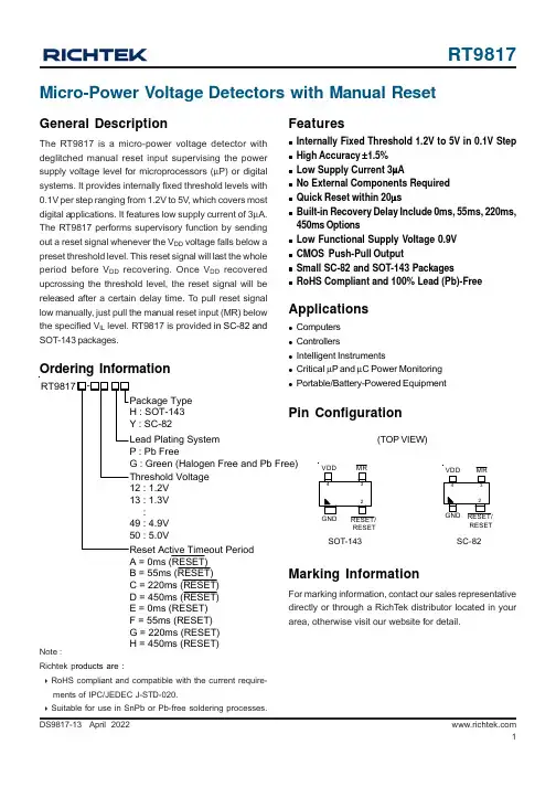
1DS9817-13 April 2022Features●Internally Fixed Threshold 1.2V to 5V in 0.1V Step ●High Accuracy ±1.5%●Low Supply Current 3μA●No External Components Required ●Quick Reset within 20μs●Built-in Recovery Delay Include 0ms, 55ms, 220ms,450ms Options●Low Functional Supply Voltage 0.9V ●CMOS Push-Pull Output●Small SC-82 and SOT-143 Packages●RoHS Compliant and 100% Lead (Pb)-FreePin ConfigurationApplications●Computers ●Controllers●Intelligent Instruments●Critical μP and μC Power Monitoring ●Portable/Battery-Powered EquipmentMicro-Power Voltage Detectors with Manual ResetOrdering InformationGeneral DescriptionThe RT9817 is a micro-power voltage detector with deglitched manual reset input supervising the power supply voltage level for microprocessors (μP) or digital systems. It provides internally fixed threshold levels with 0.1V per step ranging from 1.2V to 5V, which covers most digital applications. It features low supply current of 3μA.The RT9817 performs supervisory function by sending out a reset signal whenever the V DD voltage falls below a preset threshold level. This reset signal will last the whole period before V DD recovering. Once V DD recovered upcrossing the threshold level, the reset signal will be released after a certain delay time. To pull reset signal low manually, just pull the manual reset input (MR) below the specified V IL level. RT9817 is provided in SC-82 and SOT-143 packages.(TOP VIEW)SOT-143Marking Information For marking information, contact our sales representative directly or through a RichTek distributor located in your area, otherwise visit our website for detail.Note :Richtek p roducts are :❝RoHS compliant and compatible with the current require- ments of IPC/JEDEC J-STD-020.❝Suitable for use in SnPb or Pb-free soldering processes.SC-82RESET/RESET MRRESET/RESET MR RT9817A = 0ms (RESET)B = 55ms (RESET)C = 220ms (RESET)D = 450ms (RESET)E = 0ms (RESET)F = 55ms (RESET)G = 220ms (RESET)H = 450ms (RESET)2DS9817-13 April 2022 Functional Block DiagramTypical Application CircuitFunctional Pin DescriptionRESET/RESETMRPart StatusThe part status values are defined as below :Active : Device is in production and is recommended for new designs. Lifebuy : The device will be discontinued, and a lifetime -buy period is in effect. NRND : Not recommended for new designs.Preview : Device has been announced but is not in production. Obsolete : Richtek has discontinued the production of the device.3DS9817-13 April 2022Absolute Maximum Ratings (Note 1)●Terminal Voltage (with Respect to GND)V DD ------------------------------------------------------------------------------------------------------------------------−0.3V to 6.0V●All Other Inputs --------------------------------------------------------------------------------------------------------−0.3V to V DD +0.3V ●Input Current, I VDD -----------------------------------------------------------------------------------------------------20mA ●Power Dissipation, PD @ T A = 25°CSC-82--------------------------------------------------------------------------------------------------------------------0.25W SOT-143-----------------------------------------------------------------------------------------------------------------0.285W ●Package Thermal Resistance (Note 2)SC-82, θJA ---------------------------------------------------------------------------------------------------------------400°C SOT-143, θJA ------------------------------------------------------------------------------------------------------------350°C ●Lead Temperature (Soldering, 10sec.)---------------------------------------------------------------------------- 260°C●Storage T emperature Range ----------------------------------------------------------------------------------------−65°C to 125°C ●ESD Susceptibility (Note 3)HBM (Human Body Mode)------------------------------------------------------------------------------------------2kV MM (Machine Mode)--------------------------------------------------------------------------------------------------200VElectrical Characteristics(V= 3V, T = 25°C, unless otherwise specified)Recommended Operating Conditions (Note 4)●Junction T emperature Range ----------------------------------------------------------------------------------------−40°C to 125°C ●Ambient T emperature Range ----------------------------------------------------------------------------------------−40°C to 85°CTo be continued4DS9817-13 April 2022Note 1. Stresses listed as the above “Absolute Maximum Ratings ” may cause permanent damage to the device. These are forstress ratings. Functional operation of the device at these or any other conditions beyond those indicated in the operational sections of the specifications is not implied. Exposure to absolute maximum rating conditions for extended periods may remain possibility to affect device reliability.Note 2. θJA is measured in the natural convection at T A = 25°C on a low effective thermal conductivity test board ofJEDEC 51-3 thermal measurement standard.Note 3. Devices are ESD sensitive. Handling precautions are recommended.Note 4. The device is not guaranteed to function outside its operating conditions.5DS9817-13 April 2022Typical Operating CharacteristicsSupply Current vs. Input Voltage01234123456Input Voltage (V)S u p p l y C u r r e n t I D D (u A )Output Voltage vs. Input Voltage012345670123456Input Voltage (V)O u t p u t V o l t a g e (V)Nch Driver Output Current vs. V DS020*********120012345V DS (V)O u t p u t C u r r e n t(m A )Supply Current vs. Input Voltage01234560123456Input Voltage (V)S u p p l y C u r r e n t (u A )Nch Driver Output Current vs. V DS010********600.511.522.533.5V DS (V)O u t p u t C u r r e n t (m A )Nch Driver Output Current vs. V DS00.40.81.21.622.400.30.60.91.21.5V DS (V)O u t p u t C u r r e n t(m A )6DS9817-13 April 2022 Nch Driver Sink Current vs. Input Voltage0102030400.511.522.533.5Input Voltage (V)S i n k C u r r e n t I S I N K (m A )Supply Current vs. Input Voltage01234123456Input Voltage (V)S u p p l y C u r re n t (u A )Power-Down Reset Delay vs. Temperature051015202530354045-50-25255075100125Temperature P o w e r -D o w n R e s e t D e l a y (u s)(°C)Power-Down Reset Delay vs. Temperature051015202530354045-50-25255075100125Temperature P o w e r -D o w n R e s e t D e l a y (u s )(°C)Power-Down Reset Delay vs. Temperature03691215-50-25255075100125Temperature P o w e r -D o w n R e s e t D e l a y (u s )(°C)Nch Driver Sink Current vs. Input Voltage0102030405012345Input Voltage (V)S i n k C u r r e n t I S I N K (m A )7DS9817-13 April 2022Output Delay Time vs. Load Capacitance0.010.111010010000.00010.00100.01000.1000 1.0000Load Capacitance (uF)O u t p u t D e l a y T i m e (m s )Power-Up Reset Time-Out vs. Temperature0255075100-50-25255075100125Temperature P o w e r -U p R e s e t T im e -O u t (m s )(°C)Reset Threshold Deviation vs. Temperature1.002.003.004.005.006.00-50-25255075100125Temperature R e s e t T h r e s h o l d D e v i a t i on (V )(°C)Pch Driver Output Current vs. Input Voltage0510152025123456Input Voltage (V)O u t p u t C u r r e n t(m A )Nch Driver Output Current vs. V DS204060801001201401600123456V DS (V)N c h D r i v e r O u t p u t C ur r e n t (m A )Power-Up Reset Time-Out vs. Temperature0100200300400500-50-25255075100125Temperature P o w e r -U p R e s e t T i me -O u t (m s )(°C)8DS9817-13 April 2022 Nch Driver Output Current vs. Input Voltage1020304050600123456Input Voltage (V)N c h D r i v e r O u t p u t C u r r e n t (m A )Output Voltage vs. Input Voltage01234567123456Input Voltage (V)O u t p u tV o l t a g e (V )Power-Down Reset Time-Out vs. Temperature051015202530-50-25255075100125Temperature P ow e r -D o w n R e s e t T i m e -O u t (u s )(°C)Power Down Reset Time-Out vs. Temperature0100200300400500-50-25255075100125Temperature P o w e r D o w n R e s e t T i m e -O u t (m s )(°C)9DS9817-13 April 2022Application InformationBenefits of Highly Accurate Reset ThresholdMost μP supervisor ICs have reset threshold voltages between 1% and 1.5% below the value of nominal supply voltages.This ensures a reset will not occur within 1% of the nominal supply, but will occur when the supply is 1.5% below nom inal.10DS9817-13 April 2022SOT-143 Surface Mount Package11DS9817-13 April Richtek Technology CorporationHeadquarter5F, No. 20, Taiyuen Street, Chupei CityHsinchu, Taiwan, R.O.C.Tel: (8863)5526789 Fax: (8863)5526611Information that is provided by Richtek Technology Corporation is believed to be accurate and reliable. Richtek reserves the right to make any change in circuit design,specification or other related things if necessary without notice at any time. No third party intellectual property infringement of the applications should be guaranteed by users when integrating Richtek products into any application. No legal responsibility for any said applications is assumed by Richtek.Richtek Technology Corporation Taipei Office (Marketing)5F, No. 95, Minchiuan Road, Hsintien City Taipei County, Taiwan, R.O.C.Tel: (8862)86672399 Fax: (8862)86672377Email:*********************SC -82 Surface Mount Package。
(Chinese)DM-UL0001-04ULTEGRASW-R610SW-9071SW-R671ST-6870ST-6871FD-6870RD-6870SM-EW90-A SM-EW90-B EW-SD50EW-SD50-I SM-EWC2SM-JC40SM-JC41SM-BTR1SM-BTR2BT-DN110BT-DN110-A SM-BMR1SM-BMR2BM-DN100SM-BA01SM-BCR1SM-BCR2SM-BCC1经销商手册6870系列目录重要提示 (4)为了安全起见 (5)将使用到的工具列表 (15)安装 (17)电线接线图(总概念图) (17)电线接线图(连接器A侧) (19)安装双控手柄和刹车线 (23)前拨链器的安装 (26)安装后拨链器 (30)安装换档开关 (31)安装连接器A (39)安装连接器B (40)安装电池 (41)电线的连接 (47)连接器A的连接 (47)连接器B的连接 (49)通向双控手柄的连接 (55)在车架内为连接器B和电线布线 (57)中轴的安装 (58)卡箍的安装 (59)连接的确认 (60)电线的拆卸 (61)调整 (64)后拨链器的调整 (64)前拨链器的调整 (69)调整手柄行程 (74)给电池充电 (76)部件名称 (76)充电方法 (78)当无法充电时 (80)与个人电脑的连接和通信 (83)E-TUBE PROJECT中的可自定义设置 (83)保养 (85)更换支架外套 (85)铭牌的更换 (85)支架本体和手柄本体的拆卸 (86)安装按钮组件 (87)支架组件和手柄组件的组装 (89)导轮的更换 (90)安装B轴 (91)•经销商手册主要适合专业自行车技工使用。
对于未接受自行车安装专业培训的使用者,请勿试图利用经销商手册自行安装零部件。
如果您对手册信息的任意部分不太清楚,请勿进行安装。
请咨询购买地或当地自行车经销商地点寻求帮助。
8位Motorola单片机MC68HC908全系列编程器用户手册清华大学Motorola单片机与DSP应用开发研究中心地址:北京清华大学工程物理系馆210B房间邮编:100084电话:8610-62785779传真:8610-62782026网址:电邮:wufr@8位Motorola单片机MC68HC908全系列编程器用户手册1、简介Motorola公司的8位单片机在世界上占有很大的市场份额。
MC68HC908是Motorola公司的以Flash作为内部存储器的8位单片机系列。
面向不同的用户和场合,MC68HC908包括多种单片机型号。
比如MC68HC908JB8带有USB模块,可用于USB设备的设计;MC68HC908GP32含有丰富的IO引脚,带有SCI、SPI、AD、键盘等功能模块,是一款通用的8位单片机;MC68HC908QT,是面向低端用户的,其价格便宜,功能简约实用……MC68HC908系列单片机均以Flash作为内部存储器。
“8位Motorola单片机MC68HC908全系列编程器”以此为基础,实现对MC68HC908单片机内容Flash 的擦写,并将用户编写的程序烧写入Flash中,实现编程的功能。
2、可适用的单片机可直接进行编程的单片机型号:Pin,DIP)MC68HC908GP32 (40Pin,SDIP)MC68HC908GP32 (42Pin,SDIP)MC68HC908SR12 (42Pin,DIP)MC68HC908JL3 (28Pin,DIP)MC68HC908JK1 (20Pin,DIP)MC68HC908JK3 (20Pin,DIP)MC68HC908JB8 (20Pin,DIP)MC68HC908GR8 (28Pin,DIP)MC68HC908QY1 (16MC68HC908QY2 (16Pin,DIP)Pin,DIP)MC68HC908QY4 (16Pin,DIP)MC68HC908QT1 (8Pin,DIP)MC68HC908QT2 (8Pin,DIP)MC68HC908QT4 (8有关MC68HC908系列中其他型号的单片机及贴片封装的单片机的编程方法,用户可与中心联系。
产品规格说明书PRODUCT SPECIFICATIONFILLED BY BUYER客户名称Buyer Name客户料号Buyer Part No.客户承认签章Buyer Approved SignaturesFILLED BY LEADER文件编号Spec No.leader-1097品名Part Name 扁平振动马达Coin Type Vibration Motor型号Model No.LCM0830A1097F样品承认日期Date Samples Approved 作成 Designed by检讨 Checked by 承认 Approved by张停停2021.03.06张 冠 军 2021.03.06王 远 东2021.03.06立得微电子(惠州)有限公司Leader Micro Electronics (Huizhou) Co., Ltd.Tiger Industrial Park, Baigang, Xiaojinkou, Huizhui, Guangdong 516000, China Tel: +86-752-5853255, Fax: +86-752-5839222, Website: www. 生产地址:中国广东省惠州市小金口老虎岭工业园,邮政编码:516000规格书内容Contents of Specifications13. 外形图/ Mechanical Drawing 9/1011.环境管理物质/ Environmental Management Materials: 7/101. 适用范围/ Applicable Scope 1/102. 使用条件/ Operating Conditions 1/103. 测试条件/ Test Conditions 1/104. 初期电气性能/ Initial Electrical Characteristics 1/105. 机械性能/ Mechanical Characteristics 2/106. 耐久性能/ Reliability Characteristics 3/107. 标准测量方法/ Standard Measuring Method 5/108. 测量方法及回路图/ Measuring Method & Circuit Map 5/109. 使用注意事项/ Cautions in Use 6/1012. 包装/ Packaging 8/1010. 特性曲线图/ Characteristics Graph 6/10 14.更改记录/ Revision Records 10/102021.03.06(REV,0)说明书/Specification 编号/No.: leader-10971/10项目/Item规格/Specification2-1额定电压Rated voltage 3.0V DC 2-2使用电压范围Operating voltage 2.7~3.3V DC2-3旋转方向RotationCW(clockwise) or CCW(contrary clockwise)2-4使用环境Operating environment -20~+60℃, 10~90%RH 2-5保存环境Storage environment-30~+70℃, 10~90%RH项目/Item规格/Specification 3-1温度Temperature 25±3℃3-2湿度Humidity 65±20% RH 3-3气压Air Pressure 1013±40 hPa 3-4电源Power稳压直流电流Constant DC Current项目/Item规格/Specification 条件/Condition4-1额定转速Rated Speed 9,000rpm Min 额定电压下和额定负载下。


Mode 0 (continuous frame mode) is popular for camera pipe operation. Often, the camera pipe is enabled statically, and updates to the coefficients are only required from time to time. On demand software may enable the configuration DMA in stop mode to trigger the fetch of one single BCL. In this mode, the PVP_IPFn_TAG register is useful to match status results with a respective configuration. The new BCL only updates coefficients of processing blocks. The BCL does not alter the pipe configuration.Mode 1 (back-to-back mode) is useful in camera pipe mode when coefficients have to change every N th frame. This mode supports on-the-fly reprogramming of coefficients, but it does not support on-the-fly reprogramming of pipe configurations. The following settings must not change unless the DRAIN bit is set:•Pipe structure (PVP_xxx_CFG registers)•Fundamental operating modes (such as 1st-derivative to 2nd-derivative mode of PEC)•Input format and OPORT configuration (PVP_IPFn_CTL registers)•Horizontal size of input frame (HCNT)If any of the above settings change on-the-fly, the PVP_IPFn_PIPECTL.DRAIN bit must be set for proper operation to use Mode 2. In memory pipe mode, the PVP_IPFn_PIPECTL.DRAIN bit causes of few clock cycles of overhead depending to pipeline depth. In camera pipe mode, the PVP_IPFn_PIPECTL.DRAIN bit causes the loss of an entire frame. Operation stops after the pipe has been drained and resumes with the next incoming VSYNC signal.Whenever the next PVP job stalls until the completion event of the data output DMA is flagged either as an interrupt or as a system trigger, setting the PVP_IPFn_PIPECTL.DRAIN bit is a requirement at the appli-cation level. The data output DMA work unit does not complete as long as related data sticks in the pipe. The data in the pipe does not progress until the configuration DMA and data source grant. Such deadlock situations can be avoided by using Mode 2. Once a deadlock occurs, it can be resolved by Mode 3 opera-tion.Mode 3 (drain now instruction) is more similar to a one-time instruction than an operating mode. This mode is used whenever software needs to respond to unpredictable events. For example, while the camera >01Mode 2: Auto-Completion ModeFCNT frames are requested by the IPFn, and these feed the pipe. The last datawords are automatically pushed out, and the operation automatically completes.If a new configuration is granted by DMA or by MMR writes, the configuration isapplied for the next FCNT set of frames.All processing blocks auto-disable. A new configuration must set all wanted STARTbits again.01Mode 3: Drain Now InstructionThis combination instructs the IPFn to flush all content out of the pipe.All processing blocks auto-disable. A new configuration must set all wanted STARTbits again.Table 30-47:Operating Modes by FCNT and DRAIN Selections (Continued)FCNT DRAINModeConfiguring with Daisy Chain MethodConfiguration and coefficient memory mapped registers (MMRs) of all processing blocks are double buff-ered. Whenever PVP_IPFn_FCNT is zero and the PVP_IPF0_CFG.START and PVP_IPF1_CFG.START bits =1, the values are copied from MMR registers into application buffers at the frame boundary. Due to the pipe-lined nature of the PVP, not all values are copied at the same time. Rather, the timing of value copying is closely related to how the VSYNC of the next frame progresses through the pipe. New settings apply to the first pixel of the new frame immediately after the last pixel of the old frame has been processed. The update command is daisy chained through the pipe, starting from the IPFn blocks through to the OPFn blocks. While sequencing through the daisy chain operation, hardware clears the PVP_xxx_CFG.START bits of all involved processing blocks in MMR space. Write conflicts can occur if software attempts to write the PVP_xxx_CFG registers during the daisy chain operation.The PVP_STAT register provides two status bits that report whether a daisy chain operation is ongoing in the camera pipes (PVP_STAT.CPDC ) or in the memory pipe (PVP_STAT.MPDC ). These bits are set along with the PVP_IPF0_CFG.START or PVP_IPF1_CFG.START bit and are cleared if the output formatters have been updated.In camera pipe mode, the PVP_STAT.CPDC bit is cleared only after the daisy chain progresses through the furthest of the enabled OPFn blocks. During this time, software should not write the PVP registers. If soft-ware mistakenly does write to these registers, the event is reported by the PVP_STAT.CPWRERR and PVP_STAT.MPWRERR flags. While all status bits in the PVP_STAT register are self clearing, the PVP_ILAT register latches the events until cleared by a software handshake.A PVP block which is enabled in either the camera pipe or memory pipe can be moved to the other pipe only after the drain done command is received for the former pipe. This restriction ensures that the PVP completely processes all the pixels in one pipe and disables the PVP block, before the PVP is enables the PVP block for pixel processing in the next pipe.NOTE :Camera pipes and memory pipes can be configured by MMR writes or BCL fetches. These are sepa-rate control mechanisms and are not intended to be mixed for a given pipe during ongoing opera-tion. Before switching from one method to the other, inspect the daisy chain and drain status bits in the PVP_STAT register to ensure no operation from the other method is pending.PMA5ACU7PEC2x HCNT + 11 if 2nd derivative mode with ZCRSS=0, otherwise 1xHCNT + 6IIMn6UDS varies with settingsTable 30-48:Block Latencies (Continued)PVP Block Latency [Data Clocks]P IPELINED V ISION P ROCESSOR (PVP)P ROGRAMMING M ODELto handle the three data flows, BCS, data IN, data OUT, and optionally status data OUT. If the descrip-tors are all completed by the core, multiple PVP memory pipe jobs can be chained without any further core intervention as the DMA operations run through the chained lists and handle the multiple dataflows autonomously. The following description assumes the memory pipe is inactive, (a non initialized state PVP_CTL.MPEN =0).To run a PVP memory pipe job from the PVP memory pipe job list, the PVP first loads the memorypipe configuration into the respective shadow registers of the respective PCP elements to build the PVP memory pipe. The configuration within the shadow register is activated (transferred from shadowregister to active register) using hardware triggers (staggered transfer). This configuration stream into the shadow registers is handled by DMA 45 which is controlled by a linked descriptor list. The last valid descriptor must contain a DMA_CFG.FLOW field =0 (STOP Mode) to gracefully stop the DMA 45 aftercompleting the PVP memory pipe job list and avoid loading non valid data into PVP memory pipeconfiguration register. All DMA_CFG descriptor fields within the linked list have DMA_CFG.FLOW =6 or =7 (descriptor list mode) or alternatively DMA_CFG.FLOW =4 (descriptor array mode).A 1-dimensional DMA operation is shown in the following figure. Note however, a 2-dimensionalDMA operation can also be used.Figure 30-55:Static Linked Descriptor List for Configuration Data (BCL Data)•Job List Global TriggerAfter the first initialization of the linked descriptor list the parameter registers of DMA 45 have to beinitialized, particularly the DMA_DSCPTR_NXT and DMA_CFG register. The DMA 45 is started but thenstalls until the PVP memory pipe is enabled and the PVP_IPFn_FCNT =0.To generate a unique synchronization signal that synchronizes the Data Out (DMA 42) and Data In(DMA 43) stream, all DMA_CFG descriptor fields of DMA 45 should have the bit field DMA_CFG.TRIG =1.This generates a trigger signal after a new configuration is loaded into the shadow registers.•Job List StartAfter setting up the three DMA linked lists, the memory pipe has to be activated (PVP_CTL.MPEN =1).。
晟矽微电8位单片机MC30F6910用户手册V1.4本产品为广东晟矽微电子有限公司研制并销售,晟矽微电保留对产品在可靠性、功能和设计方面的改进作进目录1产品概要 (4)1.1产品特性 (4)1.2订购信息 (5)1.3引脚排列 (5)1.4端口说明 (6)2电气特性 (7)2.1极限参数 (7)2.2直流电气特性 (7)2.3交流电气特性 (8)2.4EEPROM特性参数 (8)3CPU与存储器 (9)3.1指令集 (9)3.2程序存储器 (10)3.3数据存储器 (11)3.4堆栈 (12)3.5控制寄存器 (12)3.6用户配置字 (14)4系统时钟 (15)4.1内部高频RC振荡器 (15)4.2内部低频RC振荡器 (15)4.3系统工作模式 (16)4.4低功耗模式 (17)5复位 (18)5.1复位条件 (18)5.2上电复位 (19)5.3外部复位 (19)5.4低电压复位 (19)5.5看门狗复位 (19)6I/O端口 (20)6.1通用I/O功能 (20)6.2内部上/下拉电阻 (20)6.3端口模式控制 (21)7定时器TIMER (22)7.1看门狗定时器WDT (22)7.2定时器T0 (23)7.3定时器T1 (25)8低电压检测LVD (31)9EEPROM存储器 (32)9.1EEPROM概述 (32)9.2EEPROM相关寄存器 (32)9.3EEPROM操作示例 (33)10FLASH烧录编程 (35)10.1FLASH在板编程 (35)11中断 (36)11.1外部中断 (36)11.2定时器中断 (36)11.3键盘中断 (36)11.4中断相关寄存器 (37)12特性曲线 (39)12.1I/O特性 (39)12.2功耗特性 (43)12.3模拟电路特性 (46)13封装尺寸 (49)13.1SOP8 (49)13.2DIP8 (49)13.3SOT23-6 (50)13.4DFN6(1×1.5 - 0.55) (50)14修订记录 (51)1产品概要1.1产品特性⏹8位CPU内核✧精简指令集,5级深度硬件堆栈✧CPU为双时钟,可在系统高/低频时钟之间切换✧系统高频时钟下F CPU可配置为F HOSC的2/4/8/16/32/64分频✧系统低频时钟下F CPU固定为F LOSC的2分频⏹程序存储器✧1K×14位FLASH型程序存储器✧支持在板不带电烧录编程,擦写次数至少1000次⏹数据存储器✧48字节SRAM型通用数据存储器,支持直接寻址、间接寻址等多种寻址方式✧64字节EEPROM型数据存储器,支持单独烧录和软件读写,擦写次数至少10000次⏹1组共6个I/O✧P1(P10~P15)✧所有端口均支持施密特输入,均可选推挽或开漏输出✧P13可复用为外部复位RST输入✧所有端口均内置上拉和下拉电阻,均可单独使能✧P10可复用为外部中断输入,支持外部中断唤醒功能✧所有端口均支持键盘中断唤醒功能,并可单独使能⏹系统时钟源✧内置高频RC振荡器(16MHz),可用作系统高频时钟源✧内置低频RC振荡器(32KHz),可用作系统低频时钟源⏹系统工作模式✧高速模式:CPU在高频时钟下运行,低频时钟源工作✧低速模式:CPU在低频时钟下运行,高频时钟源可选停止或工作✧休眠模式(低功耗模式):CPU暂停,高频时钟源停止,低频时钟源由WDT等外设决定⏹内部自振式看门狗计数器(WDT)✧与定时器T0共用预分频器✧溢出时间可配置:4.5ms/18ms/72ms/288ms(无预分频)✧工作模式可配置:始终开启、始终关闭,也可软件控制开启或关闭⏹2个定时器✧8位定时器T0,支持系统低频时钟,可实现外部计数功能,与WDT共用预分频器✧8位定时器T1,可实现外部计数、4路共周期独立占空比的PWM(可组合成2对互反的带死区互补PWM)⏹中断✧外部中断(INT),键盘中断(P10~P15)✧定时器中断(T0~T1)⏹低电压检测LVD✧ 1.8V/2.0V/2.1V/2.2V/2.4V/2.6V/2.8V/2.9V/3.0V/3.1V/3.2V/3.3V/3.6V/3.8V/4.0V/4.2V⏹ 低电压复位LVR✧ 1.8V/2.0V/2.7V/3.2V ⏹ 工作电压✧ V LVR27 ~ 5.5V @ Fcpu = 0~8MHz ✧ V LVR20 ~ 5.5V @ Fcpu = 0~4MHz ✧ V LVR18 ~ 5.5V @ Fcpu = 0~1MHz ⏹ 封装形式✧ SOP8/DIP8/SOT23-6/DFN61.2 订购信息产品名称 封装形式 备注 MC30F6910A0H SOP8 MC30F6910A0A DIP8 MC30F6910A0T SOT23-6 MC30F6910A1T SOT23-6MC30F6910A1ZLDFN61×1.5 - 0.551.3 引脚排列MC30F6910A0H/A0AMC30F6910A0H/A0ASOP8/DIP823416785GNDP10/INT/TC1/PWM1C P11/PWM1B/[PDT]P12/TC0/PWM1A/[PCK]VDDPWM1D/P15P14RST/P13MC30F6910A0TMC30F6910A0TSOT23-6234165GND [PDT]/PWM1B/P11P12/TC0/PWM1A/[PCK]VDD P14P13/RSTMC30F6910A1TMC30F6910A1TSOT23-6234165GNDP10/INT/TC1/PWM1C P11/PWM1B/[PDT][PCK]/PWM1A/TC0/P12VDDRST/P13MC30F6910A1ZLMC30F6910A1ZLDFN6(TopView)12346577 (Bottom PAD) : Don't ConnectGNDP11/PWM1B/[PDT]VDD RST/P13P12/TC0/PWM1A/[PCK]PWM1C/TC1/INT/P101.4 端口说明端口名称 类型 功能说明VDD P 电源 GND P 地P10~P15 D GPIO (推挽输出或开漏输出),内部上/下拉 INT DI 外部中断输入TC0~TC1 DI 定时器T0~T1的外部计数输入 PWM1A~PWM1DDO 定时器T1的4路PWM 输出 RST DI 外部复位输入 PCK, PDTD编程时钟/数据接口注:P-电源端口;D-数字端口,DI-数字输入,DO-数字输出;A-模拟端口,AI-模拟输入,AO-模拟输出。
Shenzhen Digital Technology Co.,ltd.PRODUCTSPECIFICATIONPRODUCT TYPE:7.0” TFT , Transmissive typeMODEL NO:Y81287VERSION:01DATE:2011.05.05Customer ApprovedCustomer:Project name:Approved by:Dept:Data:Designer QC Confirmed ApprovedShenzhen Digital Technology Co.,ltd.5F,43Bldgm Baotian Industrial Area,Xixiang,Baoan District,ShenZhen ChinaTel:(+86)755-61113669/71/72/73Fax:(+86)755-61113619RECORDS OF REVISIONDESCRIPTIONS DATE Version REVISEDISSUE2011.05.05 01FIRST深圳市德智欣科技有限公司CONTENTS1. GENERAL DESCRIPTION - - - - - - - - - - - - - - - - - - - - - - - - - -2. MECHANICAL SPECIFICATIONS - - - - - - - - - - - - - - - - -- - - - - - - -3. OUTLINE DIMENSIONS - - - - - - - - - - - - - - - - - - - - -4. INTERFACE ASSIGNMENT - - - - - - - - - - - - - - - - - - - - - - - - --------5. TIMING CHARACTERISTICS - - - - - - - - - - - - - - - - - - - - - - - ------------------------------------------------6. RESETTIMINGCHARACTERISTICS7. POWER ON/OFF SEQUENCE - - - - - - - - - - - - - - - - - - - - - - - - - - -8. INSTRUCTION TABLE - - - - - - - - - - - - - - - - - - - - - - - - - - -9. ELECTRICAL CHARACTERISTICS - - - - - - - - - - - - - - - - - - - - -10. LED BACKLIGHT CHARACTERISTICS - - - - - - - - - - - - - - - - - - -11. OPTICAL CHARACTERISTICS - - - - - - - - - - - - - - - - - - - - - - - - - -Condition -----------------------------------------------------------12. Reliability13. Inspection Standards ----------------------------------------------------14. Precaution - - - - - - - - - - - - - - - - - - - - - - - -深圳市德智欣科技有限公司1.GENERAL DESCRIPTIONThis LCM Y81287 is a 800 x 3RGB x 480 dots matrix 7.0 ”TFT LCD module. It has a TFTpanel,composed of 1200 -channel source driver and 960-channel gate driver.2. MECHANICAL SPECIFICATIONSUNIT Item Contents LCD Type 7.0” TFT-LCD, TransmissiveOutline Dimension 100(W)x164.9(H)x3.4(T) mmActive Area 85.92(W) x151.68(H) mmViewing direction 6 O’CLOCK ---Source HX8664BDriver ICGate IC HX8264DDisplay Color 16MNumber of Dots 800(RGB)x480 DotsDot Pitch (H×V)0.0642(W) x 0.1790(H) mmAssy Type COG+FPC+BL ---BACKLIGHT WHITE LED Backlight -Interface24 bit interfaceWEIGHT TBD g深圳市德智欣科技有限公司4. INTERFACE ASSIGNMENTPIN NO. SYMBOL1 Power for LED backlighr (Anode) LEDA2 Power for LED backlighr (Anode) LEDA3 Power for LED backlighr (Cathode) LEDK4 Power for LED backlighr (Cathode) LEDKground GND5 Powervoltage VCOM6 Common7 Power for Digital Circuit DVDDmodeselect MODE8 DE/SYNC9 Data input Enable DE10 Vertical Sync Input VS11 Horizontal Sync Input HS12~19 Blue data B7~B020~27 Green data G7~G028~35 Red data R7~R036 Power ground GND37 Sample clock DCLK38 Power ground GND39 Left / right selection L/R40 Up/down selection U/D41 Gate NO Voltage VGH42 Gate OFF Voltage VGL43 Power for Analog Circuit A VDD44 Global reser pin RESET45 No connection NC46 Common Voltage VCOM47 Dithering function DITHB48 Power ground GND49 No connection NC50 No connection NC深圳市德智欣科技有限公司5.TIMING CHARACTERISTICS深圳市德智欣科技有限公司6.RESET TIMING CHARACTERISTICS深圳市德智欣科技有限公司7. POWER ON/OFF SEQUENCE深圳市德智欣科技有限公司8. HX8664B&HX8264D INSTRUCTION TABLE9. ELECTRICAL CHARACTERISTICS深圳市德智欣科技有限公司深圳市德智欣科技有限公司12. Reliability Condition13.Inspection Standards 13.1 Major DefectItem NoItems to be inspected Inspection Standard Classification of defects13.1.1 Allfunctional defects1)No display2) Display abnormally3) Missing vertical, horizontal segment 4) Short circuit5)Back-light no lighting flickering and abnormal lighting.13.1.2 Missing Missing component13.1.3 OutlinedimensionOverall outline dimension beyond the drawing is not allowed.Major13.2 Cosmetic defectItem No Item ConditionRemark1 High temperatureOperating 70°C ±2°C for 240 hours2 Low temperatureOperating -20°C ±2°C for 240 hours3 High temperatureStorage 80°C ±2°C for 240 hours4 Low temperatureStorage -30°C ±2°C for 240hours5High temperature & humidity Storage50℃±5°C , 90%RH, 120 hours 6Thermal Shock Storage (No operation)-20℃ , 30min.<=> 70℃ , 30min.10 Cycles7 ESD test-8 Vibration test 10 => 55 =>10 Hz, within 1 minute;Amplitude:1.5mm.15 minutes for each Direction ( X,Y ,Z ) 9 Drop testPacked, 100CM free fall6 sides, 1 corner, 3edgesNO DEFECT IN DISPLAYING AND OPERATIONAL FUNCTION深圳市德智欣科技有限公司(i) chips on cornerX Y Z ≤2.0≤SDisregardNotes:S=contact pad lengthChips on the corner of terminal shall not be allowed to extend intothe ITO pad or expose perimeter seal. Minor(ii)Usual surface cracksX Y Z≤3.0<Inner border line of the seal DisregardMinor13.3.1Glass defect(iii)CrackCracks tend to break are not allowed.Major13.3.2 Partsalignment1) Not allow IC and FPC/heat-seal lead width is more than 50 %beyond lead pattern.2) Not allow chip or solder component is off center more than 50 % of the pad outline. 13.3.3 SMTAccording to the <Acceptability of electronic assemblies>IPC-A-610C class 2 standard. Component missing or function defect are Major defect, the others are Minor defect.Major14. Precaution14.1 Handling(1) Protect the panel from static, it may cause damage to the CMOS Gate Array IC.(2) Use fingerstalls with soft gloves in order to keep display clean during the incominginspection and assembly process.(3) If the liquid crystal material leaks from the panel, it should be kept away from theeyes or mouth. In case of contact with hands, legs or clothes, it must be washedaway thoroughly with soap.(4) The desirable cleaners are water, IPA (Isopropyl Alcohol) or Hexane. Don’t useKetone type materials (ex. Acetone), Ethyl alcohol, Toluene, Ethyl acid or Methylchloride. It might permanent damage to the polarizer due to chemical reaction.(5) Pins of I/F connector shall not be touched directly with bare hands.(6) Refrain from strong mechanical shock and / or any force to the panel. In addition todamage, this may cause improper operation or damage to the panel.(7) Note that polarizers are very fragile and could be easily damaged. Do not press orscratch the surface harder than a B pencil lead.(8) Wipe off water droplets or oil immediately. If you leave the droplets for a long time,staining and discoloration may occur.(9) If the surface of the polarizer is dirty, clean it using some absorbent cotton or soft cloth.14.2 Storage(1) Do not leave the panel in high temperature, and high humidity for a long time. It ishighly recommended to store the panel with temperature from 0 to 35℃ andrelative humidity of less than 70%.(2) The panel shall be stored in a dark place. It is prohibited to apply sunlight orfluorescent light during the store.14.3 Operation(1) The LCD shall be operated within the limits specified. Operation at values outside ofthese limits may shorten life, and/or harm display images.(2) Do not exceed the absolute maximum rating value. (the supply voltage variation,Input voltage variation in part contents and environmental temperature and so on).Otherwise the panel may be damaged.(3) If the panel displays the same pattern continuously for a long period of time, it canbe the situation when the image” Sticks” to the screen.深圳市德智欣科技有限公司。