MRF6S9045NR1中文资料
- 格式:pdf
- 大小:536.24 KB
- 文档页数:16

PCB封装库建库规则2010 11 251除环形器等射频走线要求的器件外,其他器件的原点均在器件的中心。
2位号文字为PADS Stroke Font,Size 50mil,Line Width 5mil。
放在top layer。
3小电容、电阻、电感的焊盘大小及间距暂时对原有的不作更改,其他IC的需核对器件的datasheet。
大功率功放IC也按此方式处理,至于匹配需后续设计人员自行在PADS Layout里增加,但不能更改器件库。
库里也不对大散热焊盘额外加散热孔,包括一些电源芯片、负载电阻及3DB耦合器等。
4独立外接焊盘及微带匹配线、微带耦合器、阻抗变换器等器件不外加丝印框。
5所有极性电容及二极管Pin Number均是1脚为正(A),2脚为负(K)。
6丝印极性标识,电容小尖口加“+”标识正极,二极管双划线标识负极。
7所有定位焊盘及散热焊盘的Pin Number均是在原有焊盘的基础上后加。
8PQFP TQFP等均统一为QFP命名,所有QFP封装的器件,若外形为长方形有长宽尺寸有标注,没标注默认为正方形。
Eg:QFP144-0R59双列贴片IC封装均为SO打头命名,标明管脚间距及两列管脚中心间距。
Eg:SO8-3r81-1R2710插针等接口一类的双排接口器件Pin number采用Z字型排列,其他的IC,继电器等一律采用U型排列方式。
11对于目前我司射频IC,若其datasheet里没有特别标明封装类型,则采用器件名-外形尺寸的命名法。
这只是针对datasheet上面没有注明封装名情况。
其他的按datasheet里注明的封装名。
12环形器等器件,命名采用ISO-外形主体尺寸的方式。
13电解电容命名采用CAP外径X孔间距-TM/SM。
高压电容采用CP长X宽。
其他电容常规处理。
14所有三角标志均是“1”脚标识,并非朝向标识。
不同的类型的器件其朝向标识表示不同,如接口的朝向标识是缺口,功放管的是箭头,二极管极是双划线等。

n45磁铁参数N45磁铁是一种高性能永磁材料,它也被称为钕铁硼磁铁。
它是由稀土元素钕(Nd)、铁(Fe)和硼(B)混合制成的。
N45磁铁的磁化能力非常强,可以在室温下保持高达1.4特斯拉的磁场强度。
这种高磁场强度意味着N45磁铁可以产生很大的吸力,并且在许多应用中非常有用。
N45磁铁的其他重要参数包括磁滞回线、矫顽力、矫顽力温度系数和热稳定性等,这些参数对于应用中的性能至关重要。
磁滞回线是磁化过程中的一个重要参数,它表示材料磁化程度的变化。
在常规应用中,磁滞回线不应该太大,因为这会导致磁场强度不够均匀,影响磁铁的性能。
对于N45磁铁,其磁滞回线小于1.1 kG。
矫顽力是另一个重要的磁铁参数,它表示对磁铁进行磁场矫正所需的场强大小。
通常,矫顽力越大,磁铁的磁化能力越强。
N45磁铁的矫顽力为50 kOe。
矫顽力温度系数是一个体现磁铁性能稳定性的参数,它表示磁铁的磁化能力在不同温度下的变化。
对于N45磁铁,其矫顽力温度系数约为-0.11%/℃。
热稳定性是另一个与磁铁性能相关的参数。
对于N45磁铁,在高温下仍然能够保持很高的磁场强度和磁性能,在室温下的磁场几乎不会衰减。
这种热稳定性使得N45磁铁非常适合在高温环境下使用。
N45磁铁是一种高性能永磁材料,具有非常强的磁化能力和热稳定性。
了解其相关参数对于选择合适的磁铁应用非常重要。
除了上述参数,N45磁铁的外观形状和尺寸也是应用中需要考虑的因素。
N45磁铁可以制成各种形状,包括圆柱形、方形、圆盘形、环形等等。
N45磁铁的尺寸也可以根据具体应用需求定制,以满足不同场合的要求。
在各种应用中,N45磁铁都能够发挥出其优异的磁性能与吸力。
最常见的应用包括:电机、发电机、传感器、医疗设备、航空航天、汽车、电子设备等。
在电机、发电机等领域中,N45磁铁被广泛用于永磁同步电机、直流电机等方面。
在传感器方面,N45磁铁可以作为位移传感器、角位移传感器、速度传感器、磁场传感器和探测器等等。

Cooper-WheelockAS/AH SeriesSingle & Multi-Candela AS Series Audible Strobe & AH Series Audible AppliancesGAMEWELL-FCIDescriptionThe 2-wire Cooper-Wheelock AS Series audible/visual and AH Series audible notification appliances offer many features with low current draws.Strobe options for wall-mounted models include 15/75 cd or field-selectable Multi-Candela strobes that may be set to 15, 30, 75, or 110 cd.Ceiling mounted models incorporate field-selected strobe settings of 15, 30, 75 or 95 cd.The audible notification appliances provide a field-selectable choice of either a continuous horn tone or temporal pattern (per ANSI S3.41) when constant voltage is supplied by the notification appliance cir-cuit. Each tone has three dBA settings to choose from. Additionally, the audible tone may be silenced while maintaining strobe activation.All models may be synchronized when the models are used in conjunction with the Cooper-Wheelock SM and DSM Sync Modules.The synchronization of the continuous horn tone provides the temporal pattern mandated by NFPA 72 for fire evacuation signaling. This ensures a clearly distinguishable temporal pattern when two or more audible devices are within hearing distance. If the horn tones are not synchronized, the temporal patterns may overlap. At the same time, the strobes will also be synchronized. This process is in compli-ance with ADA recommendations regarding photo-sensitive epilepsy and NFPA and UFC standards required when installing two or more visual appli-ances within a common field of view.Only two wires are required to achieve these se-quences of operation. Separate circuits for audible and visual devices are not necessary.An ISO 9000-2000 CompanyFeatures• Approvals include:- UL Standard 1971 - UL Standard 464 - New York City (MEA)- California State Fire Marshall (CSFM)• ADA/NFPA/UFC/ANSI compliant• Wall-mounted models are available with field multi-candela settings of 15, 30, 75, or 110 cd• Ceiling mounted models are available with field select-able multi-candela settings of 15, 30, 75, or 95 cd • Single candela models are available in 15/75 cd • Weatherproof models are available for outdoor use (ASWP)• Selected continuous horn or temporal pattern (ANSI 3.41)• Three (3) field dBA settings adjusted to 90, 95, or 99 dBA for both tones• Silenceable horns and non-silenceable strobes installed over the same wires• Strobes flash once per second over the regulated volt-age range• 12 & 24 VDC models with wide UL “regulated voltage range” using filtered DC or unfiltered FWR input voltage • Synchronize with SM or DSM synchronization modules• Fast installation with In/Out screw terminals using 12 to 18 AWG wiresSeries AHSeries AS# SM Sync Module is rated for 3.0 amps @ 24 VDC ## DSM Sync Module is rated for 3.0 amps per circuit.The maximum number of interconnectedDSM Modules is 20.SYNC MODULESMODEL ORDER CODE INPUTVOLTAGE (VDC)AVERAGE MEAN CURRENT@ 24VDCSM-12/24-R #636924VDC 0.028A SM-12/24-R ##637424VDC0.035AArchitects and Engineers SpecificationsThe notification appliances shall be Cooper-Wheelock Series AS audible/strobe appliances and Series AH audible appliances or approved equals. The Series AS appliance shall be listed under UL Standard 1971 (Emergency Devices for the Hearing Impaired) for indoor Fire Protection Service. The Series AH Audible shall be UL Listed under Standard 464 (Fire Protective Signaling). Both shall meet the requirements of FCC Part 15 Class B. All inputs shall be compatible with standard reverse polarity supervision of circuit wiring by a fire alarm control panel (FACP).The audible portion of the appliance shall have a minimum of three (3) field selectable settings for dBA levels and shall have a choice of continuous or temporal pattern audible output.The strobe portion of the appliance shall produce a flash rate of one (1) flash per second over the Regulated Voltage Range and shall incorporate a Xenon flashtube enclosed in a rugged Lexan ® lens. The series AS shall be of low current design. Where Multi-Candela appliances are specified, the strobe intensity shall have a minimum of four (4) field selectable settings and shall be rated per UL Standard 1971 at: 15, 30, 75, and 110 candela for wall mount, or 15, 30, 75, and 95 candela for ceiling mount. The selector switch for selecting the candela shall be tamper resistant and not accessible from the front of the appliance. The 15/75 candela strobe shall be specified when 15 cd UL Standard 1971 Listing with 75 cd on-axis is required (e.g. ADA compliance).When synchronization is required, the appliance shall be compatible with Cooper-Wheelock’s SM and DSM Sync Modules. The strobes shall not drift out of synchronization at any time during operation. If the sync module fails to operate, i.e. contacts remain closed), the strobe shall revert to a non-synchronized flash-rate. The appliance shall also be designed so that the audible signal may be silenced while maintaining strobe activation.The Series AS audible/strobe and Series AH audible shall incorporate a patented universal mounting plate that shall allow mount-ing on a single-gang, double-gang, 4-inch square, 100 mm European type backbox, or the SHBB surface backbox. If required, an NATP (Notification Appliance Trimplate) shall be provided.All notification appliances shall be backward compatible.SpecificationsModel Strobe CandelaNon-Sync Sync w SM/ or DSM 24 VDC 12 VDC Wall Mount Ceiling Mount UL MEA CSFM FM BFPAS-24MCW-FR 15/30/75/110 X X X - X - X X X X X AS-24M CW –FW 15/30/75/110 X X X - X - X X X X X AS-241575W - FR 15 (75 on Axis) X X X - X - X X X X X AS-121575W –FR 15 (75 on Axis) X X X - X - X X X X X AS-24MCC –FW 15/30/75/95 X X X - - X X * * * * ASW-P-2475W –FR 75 @ -31° F X X X - X - X X X X * AH –24-R - X X X - X X X X X X X AH –24W P-R - X X X - X X X X AH –12W P-R - X X - X X X X XOrdering InformationPart NumberDescription9024 AS-24MCW-FR 9025 AS-24M CW –FW 7405 AS-241575W - FR 3162 AS-24MCC –FW 7410 AS-121575W –FR 9012 ASW-P-2475W –FR 7892 AH –24-R 7416 AH –24W P-R 7415 AH –12W P-R7891 AH –12-R。


MBR4035PT THRU MBR4060PTSCHOTTKY RECTIFIERReverse Voltage -35 to 60 Volts Forward Current - 40.0 AmperesFEATURES♦ Plastic package has Underwriters Laboratory Flammability Classifications 94V-0♦ Dual rectifier construction, positive center-tap ♦ Metal silicon rectifier,majority carrier conduction ♦ Low power loss,high efficiency♦ High current capability, low forward voltage drop ♦ High surge capability♦ For use in low voltage, high frequency inverters, free wheeling, and polarity protection applications ♦ Guardring for overvoltage protection ♦ High temperature soldering guaranteed:250°C/10 seconds, 0.17" (4.3mm) from caseMECHANICAL DATACase:JEDEC TO-247AD molded plastic body Terminals:Lead solderable per MIL-STD-750,Method 2026Polarity:As marked Mounting Position:AnyMounting Torque:10 in.- lbs.max.Weight:0.2 ounce, 5.6 gramsMAXIMUM RATINGS AND ELECTRICAL CHARACTERISTICSRatings at 25°C ambient temperature unless otherwise specified.SYMBOLS MBR4035PT MBR4045PT MBR4050PT MBR4060PT UNITSMaximum repetitive peak reverse voltage V RRM 35455060Volts Maximum working peak reverse voltage V RMS 35455060Volts Maximum DC blocking voltageV DC 35455060Volts Maximum average forward rectified current at T C =125°CI (AV)40.0Amps Peak repetitive forward current per leg at T C =120°C (rated V R square wave, 20 KH Z )I FRM 40.0Amps Peak forward surge current, 8.3ms single half sine-wave superimposed on rated load (JEDEC Method)I FSM 400.0AmpsPeak repetitive reverse surge current (NOTE1)I RRM2.01.0AmpsMaximum instantaneous forward voltage per leg at I F =20A, T C =25°C0.700.72(NOTE 2)I F =20A, T C =125°C V F 0.600.62VoltsI F =40A, T C =25°C 0.80_I F =40A, T C =125°C 0.75_Maximum instantaneous reverse current at T C =25°C 1.0rated DC blocking voltage per leg (NOTE 2) T C =125°C I R 100.0mA Typical thermal resistance per leg (NOTE 3)R ΘJC 1.2°C/W Voltage rate of change (rated V R )dv/dt 10,000V/µs Operating junction temperature range T J -65 to +150°C Storage temperature rangeT STG-65 to +175°CNOTES:(1) 2.0µs pulse width, f=1.0 KH Z(2) Pulse test: 300µs pulse width, 1% duty cycle (3) Thermal resistance from junction to case per leg4/981o REF.Dimensions in inches and (millimeters)TO-247AD0.010.11101000.111010050100150010********11010010020030040000.10.20.30.40.50.60.70.80.91.01.11.20.010.1110500.11101001001,0005,000204060801000.0010.010.111050RATINGS AND CHARACTERISTIC CURVES MBR4035PT THRU MBR4060PTT J =150°CFIG. 1 - FORWARD CURRENT DERATING CURVECASE TEMPERATURE, °CA V E R A G E F O R W A R D C U R R E N T ,A M P E R E SFIG. 2 - MAXIMUM NON-REPETITIVE PEAK FORWARDSURGE CURRENT PER LEGNUMBER OF CYCLES AT 60 H ZP E A K F O R W A R D S U R G E C U R R E N T ,A M P E R E SFIG. 3 - TYPICAL REVERSE CHARACTERISTICSPER LEGFIG. 4 - TYPICAL REVERSE CHARACTERISTICSPER LEGI N S T A N T A N E O U S F O R W A R D C U R R E N T , A M P E R E SI N S T A N T A N E O U S R E V E R S E C U R R E N T , M I L L I A M P E R E SINSTANTANEOUS FORWARD VOLTAGE,VOLTSPERCENT OF RATED PEAK REVERSE VOLTAGE, %FIG. 5 - TYPICAL JUNCTION CAPACITANCE PER LEGJ U N C T I O N C A P A C I T A N C E , p FREVERSE VOLTAGE, VOLTST J =T J max.8.3ms SINGLE HALF SINE-WAVE (JEDEC Method)RESISTIVE OR INDUCTIVE LOADT J =75°CT J =25°CT J =25°CPULSE WIDTH=300µs 1%DUTY CYCLET J =125°CFIG . 6 - TYPICAL TRANSIENT THERMAL IMPEDANCEPER LEGt, PULSE DURATION, sec.T R A N S I E N T T H E R M A L I M P E D A N C E , °C /WMBR4035PT - MBR4045PT MBR4050PT & MBR4060PTMBR4035PT - MBR4045PT MBR4050PT & MBR4060PTMBR4035PT - MBR4045PT MBR4050PT & MBR4060PTT J =25°C f=1.0 MHz Vsig=50mVp-p。


RF Power Field Effect TransistorsN-Channel Enhancement-Mode Lateral MOSFETsDesigned for GSM and GSM EDGE base station applications with frequencies from 920 to 960 MHz. Suitable for CDMA and multicarrier amplifier applications.•Typical GSM Performance: V DD = 28 Volts, I DQ = 300 mA, P out =35.5 Watts CW, f = 960 MHz Power Gain — 19 dB Drain Efficiency — 57%•Capable of Handling 5:1 VSWR, @ 32 Vdc, 940 MHz, 70 Watts CW Output Power (3 dB Input Overdrive from Rated P out ), Designed for Enhanced Ruggedness•Typical P out @ 1 dB Compression Point ] 45 Watts CW•Typical GSM EDGE Performance: V DD = 28 Volts, I DQ = 285 mA, P out = 17.8 Watts Avg., Full Frequency Band (920-960 MHz)Power Gain — 19 dB Drain Efficiency — 42.5%Spectral Regrowth @ 400 kHz Offset = -62.5 dBc Spectral Regrowth @ 600 kHz Offset = -72 dBc EVM — 2.1% rms Features•Characterized with Series Equivalent Large-Signal Impedance Parameters •Internally Matched for Ease of Use •Integrated ESD Protection•Greater Negative Gate-Source Voltage Range for Improved Class C Operation•225°C Capable Plastic Package •RoHS Compliant•In Tape and Reel. R1 Suffix = 500 Units per 44 mm, 13 inch Reel.Table 1. Maximum RatingsRatingSymbol Value Unit Drain-Source Voltage V DSS -0.5, +66Vdc Gate-Source Voltage V GS -6.0, +10Vdc Operating VoltageV DD 32, +0Vdc Storage Temperature Range T stg -65 to +150°C Case Operating Temperature T C 150°C Operating Junction Temperature (1,2)T J225°C1.Continuous use at maximum temperature will affect MTTF.2.MTTF calculator available at /rf. Select Software & Tools/Development Tools/Calculators to access MTTF calculators by product.Document Number: MRFE6S9046NRev. 0, 5/2009Freescale Semiconductor Technical DataMRFE6S9046NR1MRFE6S9046GNR1MRFE6S9046NR1 MRFE6S9046GNR1Table 2. Thermal CharacteristicsCharacteristicSymbol Value (1,2)Unit Thermal Resistance, Junction to CaseCase Temperature 80°C, 45 W CW, 28 Vdc, I DQ = 300 mA Case Temperature 80°C, 18 W CW, 28 Vdc, I DQ = 300 mAR θJC1.31.8°C/WTable 3. ESD Protection CharacteristicsTest MethodologyClass Human Body Model (per JESD22-A114)1C (Minimum)Machine Model (per EIA/JESD22-A115) A (Minimum)Charge Device Model (per JESD22-C101)III (Minimum)Table 4. Moisture Sensitivity LevelTest MethodologyRating Package Peak TemperatureUnit Per JESD22-A113, IPC/JEDEC J-STD-0203260°CTable 5. Electrical Characteristics (T C = 25°C unless otherwise noted)CharacteristicSymbolMinTypMaxUnitOff CharacteristicsZero Gate Voltage Drain Leakage Current (V DS = 66 Vdc, V GS = 0 Vdc)I DSS ——10μAdc Zero Gate Voltage Drain Leakage Current (V DS = 28 Vdc, V GS = 0 Vdc)I DSS ——1μAdc Gate-Source Leakage Current (V GS = 5 Vdc, V DS = 0 Vdc)I GSS——1μAdcOn CharacteristicsGate Threshold Voltage(V DS = 10 Vdc, I D = 100 μAdc)V GS(th)1 2.23Vdc Gate Quiescent Voltage(V DD = 28 Vdc, I D = 300 mAdc, Measured in Functional Test)V GS(Q)2 3.14Vdc Drain-Source On-Voltage (V GS = 10 Vdc, I D = 1 Adc)V DS(on)0.10.30.4VdcDynamic Characteristics (3)Reverse Transfer Capacitance(V DS = 28 Vdc ± 30 mV(rms)ac @ 1 MHz, V GS = 0 Vdc)C rss —0.6—pF Output Capacitance(V DS = 28 Vdc ± 30 mV(rms)ac @ 1 MHz, V GS = 0 Vdc)C oss —318—pF Input Capacitance(V DS = 28 Vdc, V GS = 0 Vdc ± 30 mV(rms)ac @ 1 MHz)C iss—120—pFFunctional Tests (4) (In Freescale Test Fixture, 50 ohm system) V DD = 28 Vdc, P out = 35.5 W CW, I DQ = 300 mA, f = 960 MHzCharacteristicSymbol Min Typ Max Unit Power Gain G ps 17.519—dB Drain Efficiency ηD 5457—%Input Return LossIRL—-13-7dB1.MTTF calculator available at /rf. Select Software & Tools/Development Tools/Calculators to access MTTF calculators by product.2.Refer to AN1955, Thermal Measurement Methodology of RF Power Amplifiers. Go to /rf. Select Documentation/Application Notes - AN1955.3.Part internally matched both on input and output.4.Measurement made with device in straight lead configuration before any lead forming operation is applied.(continued)MRFE6S9046NR1 MRFE6S9046GNR1Table 5. Electrical Characteristics (T C = 25°C unless otherwise noted) (continued)CharacteristicSymbolMinTypMaxUnitTypical Performances (In Freescale GSM EDGE Reference Design T est Fixture, 50 ohm system) V DD = 28 Vdc, I DQ = 300 mA, 920-960 MHz BandwidthP out @ 1 dB Compression PointP1dB —45—W IMD Symmetry @ 44 W PEP , P out where IMD Third Order Intermodulation ` 30 dBc(Delta IMD Third Order Intermodulation between Upper and Lower Sidebands > 2 dB)IMD sym—55—MHzVBW Resonance Point(IMD Third Order Intermodulation Inflection Point)VBW res —65—MHz Gain Flatness in 40 MHz Bandwidth @ P out = 35.5 W CW G F —0.2—dB Average Deviation from Linear Phase in 40 MHz Bandwidth @ P out = 45 W CW Φ—0.9—°Average Group Delay @ P out = 45 W CW, f = 940 MHz Delay — 3.1—ns Part-to-Part Insertion Phase Variation @ P out = 45 W CW, f = 940 MHz, Six Sigma Window ΔΦ—20—°Gain Variation over Temperature (-30°C to +85°C)ΔG —0.021—dB/°C Output Power Variation over Temperature (-30°C to +85°C)ΔP1dB—0.006—dBm/°CTypical GSM EDGE Performances (In Freescale GSM EDGE Reference Design Test Fixture, 50 ohm system) V DD = 28 Vdc, I DQ = 285 mA,P out = 17.8 W Avg., 920-960 MHz EDGE Modulation Power Gain G ps —19—dB Drain Efficiency ηD —42.5—%Error Vector MagnitudeEVM — 2.1—% rms Spectral Regrowth at 400 kHz Offset SR1—-62.5—dBc Spectral Regrowth at 600 kHz OffsetSR2—-72—dBcMRFE6S9046NR1 MRFE6S9046GNR1Figure 2. MRFE6S9046NR1(GNR1) Test Circuit Schematic — GSM EDGE Reference DesignZ100.040″ x 0.450″ Microstrip Z110.321″ x 0.450″ Microstrip Z120.080″ x 0.280″ Microstrip Z130.372″ x 0.044″ Microstrip Z140.124″ x 0.044″ Microstrip Z150.200″ x 0.044″ MicrostripPCBRogers R04350, 0.020″, εr = 3.66* Line length includes microstrip bendsZ10.200″ x 0.044″ Microstrip Z20.196″ x 0.044″ Microstrip Z30.380″ x 0.044″ Microstrip Z40.321″ x 0.450″ Microstrip Z50.039″ x 0.450″ Microstrip Z6*0.281″ x 0.040″ Microstrip Z70.892″ x 0.051″ Microstrip Z8* Z9*0.751″ x 0.040″ MicrostripTable 6. MRFE6S9046NR1(GNR1) Test Circuit Component Designations and Values — GSM EDGE Reference DesignPartDescriptionPart NumberManufacturer C1, C956 pF Chip Capacitors ATC600F560BT500XT ATC C2 2.4 pF Chip Capacitor ATC600F2R4BT500XT ATC C3, C4 6.8 pF Chip Capacitors ATC600F6R8BT500XT ATC C5, C11, C1410 μF, 50 V Chip Capacitors GRM55DR61H106KA88B Murata C6, C7 3.3 pF Chip Capacitors ATC600F3R3BT500XT ATC C8 4.7 pF Chip Capacitor ATC600F4R7BT500XT ATC C10, C1339 pF Chip CapacitorsATC600F390BT500XT ATC C12470 μF, 63 V Electrolytic Capacitor MCGPR63V477M13X26-RH Multicomp R14.7 K Ω, 1/4 W Chip ResistorCRCW12064701FKEAVishayFigure 3. MRFE6S9046NR1(GNR1) Test Circuit Component Layout — GSM EDGE Reference DesignMRFE6S9046NR1 MRFE6S9046GNR1MRFE6S9046NR1 MRFE6S9046GNR1TYPICAL CHARACTERISTICS100.1100P out , OUTPUT POWER (WATTS) CW1521120181710100Figure 6. Power Gain versus Output PowerG p s , P O W E R G A I N (d B )19TWO−TONE SPACING (MHz)Figure 7. Intermodulation Distortion Productsversus Two-Tone Spacing161MRFE6S9046NR1 MRFE6S9046GNR1TYPICAL CHARACTERISTICS7014247510118163015P out , OUTPUT POWER (WATTS) CWFigure 8. Power Gain and Drain Efficiencyversus Output PowerG p s ,P O W E R G A I N (d B )22206045Figure 9. EVM versus Frequencyf, FREQUENCY (MHz)E V M , E R R O R V E C T O R M A G N I T U D E (% r m s )9800690031970940920910425S P E C T R A L R E G R O W T H @ 400 k H z (d B c )P out , OUTPUT POWER (WATTS) AVG.60200101Figure 12. EVM and Drain Efficiencyversus Output PowerE V M , E R R O R V E C T O R M A G N I T U D E (% r m s )980900920940960f, FREQUENCY (MHz)Figure 13. Power Gain versus Frequency910930950970ηD , D R A I N E F F I C I E N C Y (%)93096095018161412108642MRFE6S9046NR1 MRFE6S9046GNR1TYPICAL CHARACTERISTICS1450−520650f, FREQUENCY (MHz)Figure 14. Broadband Frequency Response15105011501050950850750G A I N (d B )1250135025090T J , JUNCTION TEMPERATURE (°C)Figure 15. MTTF versus Junction TemperatureThis above graph displays calculated MTTF in hours when the device is operated at V DD = 28 Vdc, P out = 35.5 W CW, and ηD = 57%.MTTF calculator available at /rf. Select Software & Tools/Development Tools/Calculators to access MTTF calculators by product.110130150170190210230GSM TEST SIGNALFigure 16. EDGE Spectrum−10−20−30−40−50−60−70−80−90−100200 kHzSpan 2 MHzCenter 1.96 GHz−110(d B )MRFE6S9046NR1 MRFE6S9046GNR1Z o = 10 ΩZ loadZ sourcef = 980 MHzf = 820 MHzf = 980 MHzf = 820 MHzV DD = 28 Vdc, I DQ = 285 mA, P out = 17.8 W Avg.f (MHz)Z sourceW Z load W 820 5.03 - j7.297.68 - j3.45840 4.46 - j6.69 6.97 - j3.53860 4.00 - j6.11 6.42 - j3.20880 3.62 - j5.64 5.98 - j2.87900 3.29 - j5.18 5.65 - j2.52920 3.03 - j4.75 5.40 - j2.17940 2.80 - j4.36 5.21 - j1.82960 2.61 - j3.99 5.09 - j1.479802.46 - j3.645.03 - j1.12Z source =Test circuit impedance as measured fromgate to ground.Z load=Test circuit impedance as measured fromdrain to ground.Figure 17. Series Equivalent Source and Load Impedance — GSM EDGE Reference DesignZsourceZloadOutput Matching NetworkMRFE6S9046NR1 MRFE6S9046GNR1ALTERNATIVE PEAK TUNE LOAD PULL CHARACTERISTICS29P in , INPUT POWER (dBm)48464430323133494743P o u t , O U T P U T P O W E R (d B m )NOTE: Load Pull Test Fixture Tuned for Peak P1dB Output Power @ 28 V4550515253282726232524Test Impedances per Compression LevelZ sourceΩZ load ΩP1dB7.83 - j2.011.25 - j0.52Figure 18. Pulsed CW Output Power versus Input Power @ 28 V @ 920 MHz 29P in , INPUT POWER (dBm)47454330323133484642P o u t , O U T P U T P O W E R (d B m )NOTE: Load Pull Test Fixture Tuned for Peak P1dB Output Power @ 28 V4449505152282726232524Test Impedances per Compression LevelZ sourceΩZ load ΩP1dB3.79 - j6.514.30 - j2.52Figure 19. Pulsed CW Output Power versus Input Power @ 28 V @ 960 MHz分销商库存信息:FREESCALEMRFE6S9046GNR1MRFE6S9046NR1。


Publication Date:Oct.2011<Silicon RF Power Modules >RA45H4045MRRoHS Compliance,400-450MHz 45W 12.5V,3Stage Amp.For MOBILE RADIO DESCRIPTIONThe RA45H4045MR is a 45-watt RF MOSFET Amplifier Module for 12.5-volt mobile radios that operate in the 400-to 450-MHz range.The battery can be connected directly to the drain of the enhancement-mode MOSFET transistors.Without the gatevoltage (V GG =0V),only a small leakage current flows into the drain and the RF input signal attenuates up to 60dB.The output power and drain current increase as the gate voltage increases.With a gate voltage around 4V (minimum),output power and drain current increases substantially.The nominal output power becomes available at 4.5V (typical)and 5V (maximum).At V GG =5V,the typical gate current is 1mA.This module is designed for non-linear FM modulation,but may also be used for linear modulation by setting the drain quiescent current with the gate voltage and controlling the output power with the input power.FEATURES•Enhancement-Mode MOSFET Transistors (I DD ≅0@V DD =12.5V,V GG =0V)•P out >45W,ηT >35%@V DD =12.5V,V GG =5V,P in =50mW•Broadband Frequency Range:400-450MHz•Low-Power Control Current I GG =1mA (typ)at V GG =5V•Module Size:66x 21x 9.88mm •Reverse PIN type•Linear operation is possible by setting the quiescent drain current with the gate voltage and controlling the output power with the input powerRoHS COMPLIANCE•RA45H4045MR-101is a RoHS compliant products.•RoHS compliance is indicate by the letter “G”after the Lot Marking.•This product include the lead in the Glass of electronic parts and the lead in electronic Ceramic parts.However,it is applicable to the following exceptions of RoHS Directions.1.Lead in the Glass of a cathode-ray tube,electronic parts,and fluorescent tubes.2.Lead in electronic Ceramic parts.ORDERING INFORMATION:ORDER NUMBER SUPPLY FORM RA45H4045MR-101Antistatic tray,10modules/trayMAXIMUM RATINGS (T case =+25°C,unless otherwise specified)SYMBOL PARAMETER CONDITIONS RATING UNIT V DD Drain Voltage V GG <5V17V V GG Gate Voltage V DD <12.5V,P in =0mW 6V P in Input Power 100mW P out Output Power55W T case(OP)Operation Case Temperature Range f=400-450MHz,Z G =Z L =50Ω-30to +110°C T stgStorage Temperature Range-40to +110°CAbove Parameters are guaranteed independentlyELECTRICAL CHARACTERISTICS (T case =+25°C,Z G =Z L =50Ω,unless otherwise specified)SYMBOL PARAMETERCONDITIONS MINTYPMAXUNITf Frequency Range 400-450MHz P out Output Power 45--W ηT Total Efficiency 35--%2f o 2ndHarmonic---25dBc ρin Input VSWR --3:1—I GG Gate Current V DD =12.5V V GG =5V P in =50mW-1-mA —StabilityV DD =10.0-15.2V,P in =25-70mW,P out <55W (V GG control),Load VSWR=3:1No parasitic oscillation ——Load VSWR T oleranceV DD =15.2V,P in =50mW,P out =45W (V GG control),Load VSWR=20:1No degradation or destroy—All Parameters,Conditions,Ratings and Limits are subject to change without noticeOUTPUT POWER,TOTAL EFFICIENCY,2nd ,3rd HARMONICS versus FREQUENCYand INPUT VSWR versus FREQUENCYOUTPUT POWER,POWER GAIN and OUTPUT POWER,POWER GAIN and DRAIN CURRENT versus INPUT POWERDRAIN CURRENT versus INPUTPOWER01020304050607080390400410420430440450460FREQUENCY f(MHz)O U T P U T P O W E R P o u t (W )I N P U T V S W R ρi n (-)01020304050607080T O T A L E F F I C I E N C Y ηT (%)0102030405060-15-10-55101520INPUT POWER P in (dBm)O U T P U T P O W E R P o u t (d B m )P O W E R G A I N G p (d B )4812162024D R A I N C U R RE N T I D D (A )0102030405060-15-10-505101520INPUT POWER P in (dBm)O U T P U T P O W E R P o u t (d B m )P O W E R G A I N G p (d B )04812162024D R A I N C U R RE N T I D D (A )-70-60-50-40-30-20390400410420430440450460FREQUENCY f(MHz)H A R M O N I C S (d B c )OUTPUT POWER,POWER GAIN and DRAIN CURRENT versus INPUT POWEROUTPUT POWER and DRAIN CURRENTOUTPUT POWER and DRAIN CURRENTversus DRAIN VOLTAGEversus DRAINVOLTAGE102030405060708090100246810121416DRAIN VOLTAGE V DD (V)O U T P U T P O W E R P o u t (W )02468101214161820D R A I N C U R R E N T I D D (A )010********60-15-10-55101520INPUT POWER P in (dBm)O U T P U T P O W E R P o u t (d B m )P O W E R G A I N G p (d B )4812162024D R A I N C U R R E N T I D D (A )102030405060708090100246810121416DRAIN VOLTAGE V DD (V)O U T P U T P O W E R P o u t (W )2468101214161820D R A I N C U R R E N T I D D (A )TYPICAL PERFORMANCE (T case =+25°C,Z G =Z L =50Ω,unless otherwise specified)OUTPUT POWER and DRAIN CURRENTversus DRAIN VOLTAGEOUTPUT POWER and DRAIN CURRENTOUTPUT POWER and DRAIN CURRENTversus GATE VOLTAGEversus GATE VOLTAGEOUTPUT POWER and DRAIN CURRENTversus GATEVOLTAGE010203040506070802.53 3.54 4.55 5.5GATE VOLTAGE V GG (V)O U T P U T P O W E R P o u t (W )D R A I N C U R RE N T I D D (A )102030405060708090100246810121416DRAIN VOLTAGE V DD (V)O U T P U T P O W E R P o u t (W )02468101214161820D R A I N C U R R E N T I D D (A )010203040506070802.53 3.54 4.55 5.5GATE VOLTAGE V GG (V)O U T P U T P O W E R P o u t (W )D R A I N C U R RE N T I D D (A )10203040506070802.53 3.54 4.55 5.5GATE VOLTAGE V GG (V)O U T P U T P O W E R P o u t (W )D R A I N C U R RE N T I D D (A )TYPICAL PERFORMANCE (T case =+25°C,Z G =Z L =50 ,unless otherwise specified)OUTLINE DRAWING (mm)1RF Input (P in )2Gate Voltage (V GG )3Drain Voltage (V DD )4RF Output (P out )5RF Ground (Case)TEST BLOCK DIAGRAMC1,C2:4700pF,22uF in parallel1RF Input(P in)2Gate Voltage(V GG)3Drain Voltage(V DD)4RF Output(P out)5RF Ground(Case)EQUIVALENT CIRCUITRECOMMENDATIONS and APPLICATION INFORMATION:Construction:This module consists of an alumina substrate soldered on a copper flange.For mechanical protection a plastic cap is attached by Silicone.The MOSFET transistor chips are die bonded onto metal,wire bonded to the substrate and coated by resin.Lines on the substrate(eventually inductors),chip capacitors and resistors form the bias and matching circuits. Wire leads soldered onto the alumina substrate provide DC and RF connection.Following conditions shall be avoided:a)Bending forces on the alumina substrate(for example during screwing or by fast thermal changes)b)Mechanical stress on the wire leads(for example by first soldering then screwing or by thermal expansion)c)Defluxing solvents reacting with the resin coating the MOSFET chips(for example Trichloroethylene)d)ESD,surge,overvoltage in combination with load VSWR,oscillation,etc.ESD:This MOSFET module is sensitive to ESD voltages down to1000V.Appropriate ESD precautions are required. Mounting:The heat sink flatness shall be less than50µm(not flat heat sink or particles between module and heat sink may cause the ceramic substrate in the module to crack by bending forces,either immediately when screwing or later when thermal expansion forces are added).Thermal compound between module and heat sink is recommended for low thermal contact resistance and to reduce the bending stress on the ceramic substrate caused by temperature difference to the heat sink.The module shall first be screwed to the heat sink,after this the leads can be soldered to the PCB.M3screws are recommended with tightening torque4.0to6.0kgf-cm.Soldering and Defluxing:This module is designed for manual soldering.The leads shall be soldered after the module is screwed onto the heat sink.The temperature of the lead(terminal)soldering should be lower than350°C and shorter than3second.Ethyl Alcohol is recommend for removing flux.Trichloroethylene solvents must not be used(they may cause bubbles in the coating of the transistor chips which can lift off the bond wires).Thermal Design of the Heat Sink:At P out=45W,V DD=12.5V and P in=50mW each stage transistor operating conditions are:Stage P in(W)P out(W)R th(ch-case)(°C/W)I DD@ηT=35%(A)V DD(V)1st0.05 2.023.00.242nd 2.012.0 2.4 2.803rd12.045.0 1.2 6.8012.5The channel temperatures of each stage transistor T ch=T case+(V DD x I DD-P out+P in)x R th(ch-case)are: T ch1=T case+(12.5V x0.24A–2.0W+0.05W)x23.0°C/W=T case+24.2°CT ch2=T case+(12.5V x2.80A-12.0W+2.0W)x2.4°C/W=T case+60.0°CT ch3=T case+(12.5V x6.80A-45.0W+12.0W)x1.2°C/W=T case+62.4°CFor long term reliability the module case temperature T case is better kept below90°C.For an ambient temperature T air=60°C and P out=45W the required thermal resistance R th(case-air)=(T case-T air)/((P out/ηT)-P out+P in)of the heat sink,including the contact resistance,is:R th(case-air)=(90°C-60°C)/(45W/35%–45W+0.05W)=0.36°C/WWhen mounting the module with the thermal resistance of0.36°C/W,the channel temperature of each stage transistor is: T ch1=T air+54.2°CT ch2=T air+90.0°CT ch3=T air+92.4°C175°C maximum rating for the channel temperature ensures application under derated conditions.Output Power Control:Depending on linearity following2methods are recommended to control the output power:a)Non-linear FM modulation:By Gate voltage V GG.When the Gate voltage is close to zero,the RF input signal is attenuated up to60dB and only a small leakage current is flowing from the battery into the Drain.Around V GG=4V the output power and Drain current increases strongly.Around V GG=4.5V,latest at V GG=5V,the nominal output power becomes available.b)Linear AM modulation:By RF input power P in.The Gate voltage is used to set the Drain quiescent current for the required linearity.Oscillation:To test RF characteristic this module is put on a fixture with2bias decoupling capacitors each on Gate and Drain,a 4.700pF chip capacitor,located close to the module,and a22µF(or more)electrolytic capacitor.When an amplifier circuit around this module shows oscillation following may be checked:a)Do the bias decoupling capacitors have a low inductance pass to the case of the module?b)Is the load impedance Z L=50Ω?c)Is the source impedance Z G=50Ω?ATTENTION:1.High Temperature;This product might have a heat generation while operation,Please take notice that have apossibility to receive a burn to touch the operating product directly or touch the product until cold after switch off.At the near the product,do not place the combustible material that have possibilities to arise the fire.2.Generation of High Frequency Power;This product generate a high frequency power.Please take notice thatdo not leakage the unnecessary electric wave and use this products without cause damage for human and property per normal operation.3.Before use;Before use the product,Please design the equipment in consideration of the risk for human andelectric wave obstacle for equipment.PRECAUTIONS FOR THE USE OF MITSUBISHI SILICON RF POWER DEVICES:1.The specifications of mention are not guarantee values in this data sheet.Please confirm additional detailsregarding operation of these products from the formal specification sheet.For copies of the formal specification sheets,please contact one of our sales offices.2.RA series products(RF power amplifier modules)and RD series products(RF power transistors)are designedfor consumer mobile communication terminals and were not specifically designed for use in other applications.In particular,while these products are highly reliable for their designed purpose,they are not manufactured under a quality assurance testing protocol that is sufficient to guarantee the level of reliability typically deemed necessary for critical communications elements and In the application,which is base station applications and fixed station applications that operate with long term continuous transmission and a higher on-off frequency during transmitting,please consider the derating,the redundancy system,appropriate setting of the maintain period and others as needed.For the reliability report which is described about predicted operating life time of Mitsubishi Silicon RF Products,please contact Mitsubishi Electric Corporation or an authorized Mitsubishi Semiconductor product distributor.3.RD series products use MOSFET semiconductor technology.They are sensitive to ESD voltage thereforeappropriate ESD precautions are required.4.In the case of use in below than recommended frequency,there is possibility to occur that the device isdeteriorated or destroyed due to the RF-swing exceed the breakdown voltage.5.In order to maximize reliability of the equipment,it is better to keep the devices temperature low.It isrecommended to utilize a sufficient sized heat-sink in conjunction with other cooling methods as needed(fan, etc.)to keep the channel temperature for RD series products lower than120deg/C(in case of Tchmax=150deg/C),140deg/C(in case of Tchmax=175deg/C)under standard conditions.6.Do not use the device at the exceeded the maximum rating condition.In case of plastic molded devices,theexceeded maximum rating condition may cause blowout,smoldering or catch fire of the molding resin due to extreme short current flow between the drain and the source of the device.These results causes in fire or injury.7.For specific precautions regarding assembly of these products into the equipment,please refer to thesupplementary items in the specification sheet.8.Warranty for the product is void if the products protective cap(lid)is removed or if the product is modified in anyway from it’s original form.9.For additional“Safety first”in your circuit design and notes regarding the materials,please refer the last page ofthis data sheet.10.Please refer to the additional precautions in the formal specification sheet.©2011MITSUBISHI ELECTRIC CORPORATION.ALL RIGHTS RESERVED.。

|慈东钢种查询|产品中文产品类别慈东合金阿里巴巴慈东特钢阿里巴巴首页 >> 公司新闻 >> 产品知识AMS 相关高温耐蚀不锈钢及合金表AMS 相关高温耐蚀不锈钢及合金表USA AMS-Index-Nr.Metal SpecificationDelivery Forms UNS- Nummer AMS 5500 Alloy 30302 Laminated Sheet S30200 AMS 5501 Alloy 30304 Sheet, Strip, Foil S30400 AMS 5502 Alloy 5502 cancelled ./. AMS 5503 Alloy 51430 Sheet, Strip, Plate S43000 AMS 5504 Alloy 51410 Sheet, Strip, Plate S41000 AMS 5505 Alloy 51410 Mod Sheet, Strip, Plate S41000 AMS 5506 Alloy 51420 Sheet, Strip, Plate S42000 AMS 5507 Alloy 30316L Sheet, Strip, Plate S31603 AMS 5508 Alloy Greek Ascoloy Sheet, Strip, Plate S41800 AMS 5509 Alloy 5509 cancelled ./. AMS 5510 Alloy 30321 Sheet, Strip, Plate S32100 AMS 5511 Alloy 304L Sheet, Strip, Plate S30403 AMS 5512 Alloy 30347 Sheet, Strip, Plate S34700 AMS 5513 Alloy 30304 Sheet, Strip, Plate S30400 AMS 5514 Alloy 30305 Sheet, Strip, Plate S30500 AMS 5515 Alloy 30302 Sheet, Strip, Plate S30200 AMS 5516 Alloy 30302 Sheet, Strip, Plate S30200 AMS 5517 Alloy 30301 Sheet, Strip S30100 AMS 5518 Alloy 30301 Sheet, Strip S30100 AMS 5519 Alloy 30301 Sheet, StripS30100 AMS 5520 Alloy PH 15-7Mo Sheet, Strip, Foil, Plate S15700 AMS 5521 Alloy 30310S Sheet, Strip, Plate S31008 AMS 5522 Alloy 5522 cancelled ./. AMS 5523 Alloy 30309S Sheet, Strip, Plate S30908 AMS 5524 Alloy 30316 Sheet, Strip, Plate S31600 AMS 5525 Alloy A286 Sheet, Strip, Plate S66286 AMS 5526 Alloy 19-9DL Sheet, Strip, Plate K63198 AMS 5527 Alloy 5527 cancelled ./. AMS 5528 Alloy 17-7PH Sheet, Strip, Plate S17700 AMS 5529 Alloy 17-7PH Sheet, Strip S17700 AMS 5530 Alloy Hastelloy C Sheet, Strip, Plate N10002 AMS 5531 Alloy 5531 cancelled ./. AMS 5532 Alloy R30155 Sheet, Strip, Plate N-155 AMS 5533 Alloy 5533 cancelled ./. AMS 5534 Alloy 5534 cancelled ./. AMS 5535 Alloy 5535 cancelled ./. AMS 5536 Alloy Hastelloy X Sheet, Strip, Plate N06002 AMS 5537 Alloy L-605 Sheet, Strip, Foil, Plate R30605 AMS 5538 Alloy 5538 cancelled ./. AMS 5539 Alloy 5539 cancelled ./. AMS 5540 Alloy Inconel 600 Sheet, Strip, Plate N06600 AMS 5541 Alloy Inconel 722 Sheet, Strip N07722 AMS 5542 Alloy Sheet, Strip, Plate N07750 AMS 5543 Alloy 5543 cancelled ./. AMS 5544 Alloy Waspaloy Sheet, Strip, Plate N07001 AMS 5545 Alloy Rene 41 Sheet, Strip, Plate N07041 AMS 5546 Alloy AM-350 Sheet, Strip S35000 AMS 5547 Alloy AM-355 Sheet, Strip S35500 AMS 5548 Alloy AM-350 Sheet, Strip S35000 AMS 5549 Alloy AM-355 PlateS35500 AMS 5550 Alloy Inconel 702 Sheet, Strip, Plate N07702 AMS 5551 Alloy 5551 cancelled ./. AMS 5552 Alloy Incoloy 801 Sheet, Strip, Plate N08801 AMS 5553 Alloy Nickel 201 Sheet, Strip N02201 AMS 5554 Alloy AM-350Seamless TubingS35000AMS 5555 Alloy Nickel 205 Wire N02205 AMS 5556 Alloy 30347 Seamless or welded Tubing - Hydraulic Tubing S34700 AMS 5557 Alloy 30321 Seamless or welded Tubing - Hydraulic Tubing S32100 AMS 5558 Alloy 30347 Seamless or welded Tubing - Hydraulic Tubing S34700 AMS 5559 Alloy 30321 Seamless or welded Tubing - Hydraulic Tubing S32100 AMS 5560 Alloy 30304 Seamless or welded Tubing - Hydraulic Tubing S30400 AMS 5561 Alloy 21-6-9 Seamless or welded Tubing - Hydraulic Tubing S21900 AMS 5562 Alloy 21-6-9 Seamless or welded Tubing - Hydraulic Tubing S21904 AMS 5563 Alloy 30304 Seamless or welded Tubing - Hydraulic Tubing S30400 AMS 5564 Alloy 30304 Seamless or welded Tubing - Hydraulic Tubing S30400 AMS 5565 Alloy 30304 Seamless or welded Tubing - Hydraulic Tubing S30400 AMS 5566 Alloy 30304 Seamless or welded Tubing - Hydraulic Tubing S30400 AMS 5567 Alloy 30304 Seamless or welded Tubing - Hydraulic Tubing S30400 AMS 5568 Alloy 17-7PH Seamless or welded Tubing - Hydraulic Tubing S17700 AMS 5569 Alloy 30304I Seamless or welded Tubing - Hydraulic Tubing S30403 AMS 5570 Alloy 30321 Seamless or welded Tubing - Hydraulic Tubing S32100 AMS 5571 Alloy 30347 Seamless or welded Tubing - Hydraulic Tubing S34700 AMS 5572 Alloy 30310S Seamless or welded Tubing - Hydraulic Tubing S31008 AMS 5573 Alloy 30316 Seamless or welded Tubing - Hydraulic Tubing S31600 AMS 5574 Alloy 30309S Seamless or welded Tubing - Hydraulic Tubing S30908 AMS 5575 Alloy 30347 Seamless or welded Tubing - Hydraulic Tubing S34700 AMS 5576 Alloy 30321 Seamless or welded Tubing - Hydraulic Tubing S32100 AMS 5577 Alloy 30310 Seamless or welded Tubing - Hydraulic Tubing S31008 AMS 5578 Alloy Custom 455 Seamless or welded Tubing - Hydraulic Tubing S45500 AMS 5579 Alloy 19-9DL Seamless or welded Tubing - Hydraulic Tubing S63198 AMS 5580 Alloy Inconel 600 Seamless or welded Tubing - Hydraulic Tubing N06600 AMS 5581 Alloy Inconel 625 Seamless or welded Tubing - Hydraulic Tubing N06625 AMS 5582 Alloy Inconel X750 Seamless or welded Tubing - Hydraulic Tubing N07750 AMS 5583 Alloy Inconel X750 Seamless or welded Tubing - Hydraulic Tubing N07750 AMS 5584 Alloy 30316I Seamless or welded Tubing - Hydraulic Tubing S31603 AMS 5585 Alloy N-155 Seamless or welded Tubing - Hydraulic Tubing R30155 AMS 5586 Alloy Waspaloy Seamless or welded Tubing - Hydraulic Tubing N07001 AMS 5587 Alloy Hastelloy X Seamless or welded Tubing - Hydraulic Tubing N06002 AMS 5588 Alloy Hastelloy X Seamless or welded Tubing - Hydraulic Tubing N06002 AMS 5589 Alloy Inconel 718 Seamless or welded Tubing - Hydraulic Tubing N07718 AMS 5590 Alloy Inconel 718 Seamless or welded Tubing - Hydraulic Tubing N07718 AMS 5591 Alloy 51410 Seamless or welded Tubing - Hydraulic Tubing N41000 AMS 5592 Alloy RA 330 Sheet, Strip, Plate N08330 AMS 5593 Alloy RA 333 Sheet, Strip, Plate N06333 AMS 5594 Alloy 5594 cancelled ./.AMS 5595 Alloy 21-6-9 Sheet, Strip, Plate S21904 AMS 5596 Alloy Inconel 718 Sheet, Strip, Foil, Plate N07718 AMS 5597 Alloy Inconel 718 Sheet, Strip, Plate N07718 AMS 5598 Alloy Inconel X750 Sheet, Strip, Plate N07750 AMS 5599 Alloy Inconel 625 Sheet, Strip, Plate N06625 AMS 5600 Alloy 302 Laminated Sheet S30200 AMS 5601 Alloy 5601 cancelled ./.AMS 5602 Alloy 5602 cancelled ./.AMS 5603 Alloy PH14-8Mo Sheet, Strip - CANCELLED S14800 AMS 5604 Alloy 17-4PH Sheet, Strip, Plate S17400 AMS 5605 Alloy Inconel 706 Sheet, Strip, Plate N09706 AMS 5606 Alloy Inconel 706 Sheet, Strip, Plate N09706 AMS 5607 Alloy Hastelloy N Sheet, Strip, Plate N10003 AMS 5608 Alloy Haynes 188 Sheet, Strip, Plate R30188 AMS 5609 Alloy 51410 Mod Bars, Wire, Forgings, Tubing, Rings S41040 AMS 5610 Alloy 51416 / 51416Se Bars, Wire, Forgings S41623 AMS 5611 Alloy 51410 Mod Bars, Wire, Forgings, Tubing, Rings S4100I AMS 5612 Alloy 51410 Mod Bars, Wire, Forgings, Tubing, Rings S4100I AMS 5613 Alloy 51410 Bars, Wire, Forgings, Tubing, Rings S41000 AMS 5614 Alloy Bars, Wire, Forgings S41025 AMS 5615 Alloy 5615 cancelled ./.AMS 5616 Alloy Greek Ascoloy Bars, Wire, Forgings, Tubing, Rings S41800 AMS 5617 Alloy Cusiom 455 Bars, Wire, Forgings S45500 AMS 5618 Alloy 51440C Bars, Wire, Forgings S44004 AMS 5619 Alloy 5619 cancelled ./.AMS 5620 Alloy 51420F Bars, Wire, Forgings S42023 AMS 5621 Alloy 51420 Bars, Wire, Forgings S42000 AMS 5622 Alloy 17-4PH Bars, Wire, Forgings, Tubing, Rings, Forgings S17400 AMS 5623 Alloy Bars, Wire, Forgings, Tubing, Rings, Forgings K91456Alloy Bars, Wire, Forgings, Tubing, Rings, Forgings K91505AMS 5625 Alloy Bars, Wire, Forgings, Tubing, Rings, Forgings K91456AMS 5626 Alloy TI Bars, Wire, Forgings, Tubing, Rings, Forgings TI2001AMS 5627 Alloy 51430 Bars, Wire, Forgings, Tubing, Rings S43000AMS 5628 Alloy 51431 Bars, Wire, Forgings, Tubing S43100AMS 5629 Alloy PH 13-8Mo Bars, Forgings, Rings, Extrusions S13800AMS 5630 Alloy 51440C Bars, Wire, Forgings S44004AMS 5631 Alloy 51440A Bars, Forgings S44002AMS 5632 Alloy 51440FSe / 51440FBars, Wire, forgings S44020 / S44023 AMS 5633 Alloy 5633 cancelled ./.AMS 5634 Alloy 5634 cancelled ./.AMS 5635 Alloy 303Pb Bars, Wire, Forgings S30360AMS 5636 Alloy 30302 Bars, Wire S30200AMS 5637 Alloy 30302 Bars, Wire S30200AMS 5638 Alloy 303MA Bars, Forgings S30345AMS 5639 Alloy 30304 Bars, Wire, Forgings, Tubing, Rings S30400AMS 5640 Alloy 30303 Bars, Wire, Forgings S30300AMS 5640 Alloy 30303 Mod Bars, Wire, Forgings S30310AMS 5640 Alloy 30303 Se Bars, Wire, Forgings S30323AMS 5641 Alloy 30303 Se Bars, Wire, Forgings S30323AMS 5642 Alloy Bars, Wire, Forgings S34720 / S34723 AMS 5643 Alloy 17-4PH Bars, Wire, Forgings, Tubing, Rings S17400AMS 5644 Alloy 17-7PH Bars, Wire, Forgings, Tubing, Rings, Forgings S17700AMS 5645 Alloy 30321 Bars, Wire, Forgings, Tubing, Rings S32100AMS 5646 Alloy 30347 Bars, Wire, Forgings, Tubing, Rings S34700AMS 5647 Alloy 304L Bars, Wire, Forgings, Tubing, Rings S30403AMS 5648 Alloy 30316 Bars, Wire, Forgings, Tubing, Rings S31600AMS 5649 Alloy 316FM Bars, Wire, Forgings J92200AMS 5650 Alloy 30309S Bars, Wire, Forgings, Tubing, Rings S30908AMS 5651 Alloy 30310 Bars, Wire, Forgings, Tubing, Rings S31008AMS 5652 Alloy 30314 Bars, Wire, Forgings, Tubing, Rings S31400AMS 5653 Alloy 30316L Bars, Wire, Forgings, Tubing, Rings S31603AMS 5654 Alloy 30347 Bars, Wire, Forgings, Tubing, Rings S34700AMS 5655 Alloy 422 Bars, Wire, Forgings S42200AMS 5656 Alloy 21-6-9 Bars, Wire, Forgings, Extrusions, Rings S21904AMS 5657 Alloy PH15-7Mo Bars, Forgings S15700AMS 5658 Alloy 5658 cancelled S15500AMS 5659 Alloy 15-5PH Bars, Wire, Forgings, Extrusions, Rings S15500AMS 5660 Alloy Incoloy 901 Bars, Forgings N09901AMS 5661 Alloy Incoloy 901 Mod Bars, Forgings, Rings N09901AMS 5662 Alloy Inconel 718 Bars, Forgings, Rings N07718AMS 5663 Alloy Inconel 718 Bars, Forgings, Rings N07718AMS 5664 Alloy Inconel 718 Bars, Forgings, Rings N07718AMS 5665 Alloy Inconel 600 Bars, Forgings, Rings N06600AMS 5666 Alloy Inconel 625 Bars, Forgings, Extrusions, Rings N06625AMS 5667 Alloy Inconel X750 Bars, Forgings, Rings N07750AMS 5668 Alloy Inconel X750 Bars, Forgings, Rings N07750AMS 5669 Alloy Inconel X750 Bars, Forgings, Rings N07750AMS 5670 Alloy Inconel X750 Bars, Forgings, Rings N07750AMS 5671 Alloy Inconel X750 Bars, Forgings, Rings N07750AMS 5672 Alloy Custom 455 Bars, Forgings, Rings S45500AMS 5673 Alloy 5673 cancelled S17700AMS 5674 Alloy 30347 Wire S34700AMS 5675 Alloy FM92 Wire N07092AMS 5676 Alloy Nichrome V Wire N06003AMS 5677 Alloy Nichrome V cancelled N06003AMS 5678 Alloy 17-7PH Wire S17700AMS 5679 Alloy FM62 Wire N06062AMS 5680 Alloy SAE 30347 Wire S34781AMS 5681 Alloy 30347 Electrodes W34710AMS 5682 Alloy Nichrome V Rods, Wire ./.AMS 5683 Alloy 42 Rods, Wire ./.AMS 5684 Alloy Inconel WE 132 cancelled, Electrodes W86132AMS 5685 Alloy 30305 Rods, Wire S30500AMS 5686 Alloy 30305 Rods, Wire S30500AMS 5687 Alloy Inconel 600 Rods, Wire N06600AMS 5688 Alloy 30302 Rods, Wire S30200AMS 5689 Alloy 30321 Rods, Wire S32100AMS 5690 Alloy 30316 Rods, Wire S31600Alloy 30316 Rods, Wire W31610 AMS 5692 Alloy Rods, Wire S31680 AMS 5693 Alloy 30302 cancelled S30200 AMS 5694 Alloy Rods, Wire S31080 AMS 5695 Alloy 30310 cancelled W31010 AMS 5696 Alloy 30316 Rods, Wire S31683 AMS 5697 Alloy 30304 Rods, Wire S30400 AMS 5698 Alloy Inconel X750 Rods, Wire N07750 AMS 5699 Alloy Inconel X750 Rods, Wire N07750 AMS 5700 Alloy TPA Bars, Forgings, Rings S66009 AMS 5701 Alloy Inconel 706 Bars, Forgings, Rings N09706 AMS 5702 Alloy Inconel 706 Bars, Forgings, Rings N09706 AMS 5703 Alloy Inconel 706 Bars, Forgings, Rings N09706 AMS 5704 Alloy Waspaloy Bars, Forgings, RingsAMS 5705 Alloy CNS Bars, Forgings, Rings S63005 AMS 5706 Alloy Waspaloy Bars, Forgings, Rings N07001 AMS 5707 Alloy Waspaloy Bars, Forgings, Rings N07001 AMS 5708 Alloy Waspaloy Bars, Forgings, Rings N07001 AMS 5709 Alloy Waspaloy Bars, Forgings N07001 AMS 5710 Alloy XB Bars, Forgings S65006 AMS 5711 Alloy Hastelloy S Bars, Forgings, Rings N06635 AMS 5712 Alloy Rene 41 Bars, Forgings, Rings N07041 AMS 5713 Alloy Rene 41 Bars, Forgings, Rings N07041 AMS 5714 Alloy Inconel 722 Bars, Forgings, Rings N07722 AMS 5715 Alloy Inconel 601 Bars, Forgings, Rings N06601 AMS 5716 Alloy RA-330 Bars, Wire, Forgings, Rings N08330 AMS 5717 Alloy RA-333 Bars, Forgings, Rings N06333 AMS 5718 Alloy Jethele M-152 Bars, Forgings, Tubing, Rings S64152 AMS 5719 Alloy Jethele M-152 Bars, Wire, Forgings, Rings, Extrusions S64152 AMS 5720 Alloy 5720 cancelled ./.AMS 5721 Alloy 5721 cancelled ./.AMS 5722 Alloy 5722 cancelled ./.AMS 5723 Alloy 5723 cancelled ./.AMS 5724 Alloy 5724 cancelled ./.AMS 5725 Alloy 5725 cancelled ./.AMS 5726 Alloy A286 Bars, Wire S66286 AMS 5727 Alloy 5727 cancelled ./.AMS 5728 Alloy 5728 cancelled ./.AMS 5729 Alloy 5729 cancelled ./.AMS 5730 Alloy 5730 cancelled ./.AMS 5731 Alloy A286 Bars, Wire, Forgings, Tubing, Rings S66286 AMS 5732 Alloy A286 Bars, Wire, Forgings, Tubing, Rings S66286 AMS 5733 Alloy Discaloy Bars, Forgings S66220 AMS 5734 Alloy A286 Bars, Wire, Forgings, Tubing S66286 AMS 5735 Alloy Bars, Forgings, Tubing, Rings K66286 AMS 5736 Alloy Bars, Forgings, Tubing, Rings K66286 AMS 5737 Alloy A286 Bars, Wire, Forgings, Tubing S66286 AMS 5738 Alloy 30303F Bars, Wire, Forgings, Tubing S30323 AMS 5739 Alloy Almar 362 Bars, Forgings, Rings S36200 AMS 5740 Alloy Almar 362 Bars, Forgings, Rings S36200 AMS 5741 Alloy 5741 cancelled ./.AMS 5742 Alloy 5742 cancelled ./.AMS 5743 Alloy AM-355 Bars, Forgings S35500 AMS 5744 Alloy AM-355 Bars, Forgings S35500 AMS 5745 Alloy AM-350 Bars, Forgings S35000 AMS 5746 Alloy D-979 Bars, Forgings N09979 AMS 5747 Alloy Inconel X750 Bars, Forgings, Rings N07750 AMS 5748 Alloy 5748 cancelled ./.AMS 5749 Alloy BG-42 Bars, Wire, Forgings, Tubing S42700 AMS 5750 Alloy Hastelloy C Bars, Forgings, Rings N10002 AMS 5751 Alloy Udimet-500 Bars, Forgings, Rings N07500 AMS 5752 Alloy 5752 cancelled ./.AMS 5753 Alloy 5753 cancelled ./.AMS 5754 Alloy Hastelloy X Bars, Forgings, Rings N06002 AMS 5755 Alloy Hastelloy W Bars, Forgings, Rings N10004 AMS 5756 Alloy 5756 cancelled ./.AMS 5757 Alloy 5757 cancelled ./.AMS 5758 Alloy MP-35N Bars, Wire, Forgings, Tubing R30035 AMS 5759 Alloy L-605 Bars, Forgings, Rings R30605AMS 5760 Alloy 5760 cancelled ./.AMS 5761 Alloy 5761 cancelled ./.AMS 5762 Alloy 203EZ Bars, Wire, Forgings S20300AMS 5763 Alloy Custom 450 Bars, Forgings, Tubing, Rings S45000AMS 5764 Alloy 22-13-5 Bars, Wire, Forgings, Extrusions, Rings S20910AMS 5765 Alloy 5765 cancelled ./.AMS 5766 Alloy Incoloy 800 Bars, Forgings N08800AMS 5767 Alloy 5767 cancelled ./.AMS 5768 Alloy N-155 Bars, Wire, Forgings, Rings R30155AMS 5769 Alloy N-155 Bars, Forgings, Rings R30155AMS 5770 Alloy 5770 cancelled ./.AMS 5771 Alloy Hastelloy N Bars, Forgings, Rings N10003AMS 5772 Alloy Haynes 188 Bars, Forgings, Rings R30188AMS 5773 Alloy Custom 450 Bars, Wire, Forgings, Tubing, Rings S45000AMS 5774 Alloy AM-350 Bars, Wire, Forgings, Tubing, Rings S35080AMS 5775 Alloy 350 Bars, Wire, Forgings, Tubing, Rings W35010AMS 5776 Alloy 51410 Bars, Wire, Forgings, Tubing, Rings S41001AMS 5777 Alloy 51410 Bars, Wire, Forgings, Tubing, Rings W41010AMS 5778 Alloy FM69 Bars, Wire, Forgings, Tubing, Rings N07069AMS 5779 Alloy Inconel X750 Bars, Wire, Forgings, Tubing, Rings N07750AMS 5780 Alloy AM-355 Bars, Wire, Forgings, Tubing, Rings S35500AMS 5781 Alloy 5781 cancelled ./.AMS 5782 Alloy 19-9 W Mo Bars, Wire, Forgings, Tubing, Rings S63197AMS 5783 Alloy 5783 cancelled ./.AMS 5784 Alloy 29-9 Bars, Wire, Forgings, Tubing, Rings S64299AMS 5785 Alloy 29-9 cancelled ./.AMS 5786 Alloy Hastelloy W Bars, Wire, Forgings, Tubing, Rings N10004AMS 5787 Alloy 5787 cancelled ./.AMS 5788 Alloy Stellite 6 Hard Facing Rods, Wire R30006AMS 5789 Alloy Stellite 31 Bars, Wire, Forgings, Tubing, Rings R30031AMS 5790 Alloy Bars, Wire, Forgings, Tubing, Rings S34780SprayPlasmaAMS 5791 Alloy Powder,SprayAMS 5792 Alloy Powder,PlasmaAMS 5793 Alloy Powder, Plasma SprayAMS 5794 Alloy N-155 Bars, Wire, Forgings, Tubing, Rings R30155AMS 5795 Alloy N-155 Bars, Wire, Forgings, Tubing, Rings W73155AMS 5796 Alloy L-605 Bars, Wire, Forgings, Tubing, Rings R30605AMS 5797 Alloy L-605 Bars, Wire, Forgings, Tubing, Rings W73605AMS 5798 Alloy Hastelloy X Bars, Wire, Forgings, Tubing, Rings N06002AMS 5799 Alloy 5799 cancelled ./.AMS 5800 Alloy Rene 41 Bars, Wire, Forgings, Tubing, Rings N07041AMS 5801 Alloy Haynes 188 Bars, Wire, Forgings, Tubing, Rings R30188AMS 5802 Alloy Bars, Wire, Forgings, Tubing, Rings N19907AMS 5803 Alloy 17-4 PH Bars, Wire, Forgings, Tubing, Rings S17480AMS 5804 Alloy A286 Bars, Wire, Forgings, Tubing, Rings S66286AMS 5805 Alloy A286 Bars, Wire, Forgings, Tubing, Rings S66286AMS 5806 Alloy incoloy 903 Bars, Wire, Forgings, Tubing, Rings N19903AMS 5808 Alloy Bars, Wire, Forgings, Tubing, RingsAMS 5809 Alloy 5809 cancelled ./.Wire S66286 AMS 5810 Alloy FlatWireAMS 5811 Alloy FlatAMS 5812 Alloy WPH-15-7Mo-VM Flat Wire S15789AMS 5813 Alloy 5813 cancelled ./.AMS 5814 Alloy Wire R30918 AMS 5817 Alloy Greek Ascoloy Wire S41800AMS 5818 Alloy WireAMS 5819 Alloy Wire R30021AMS 5821 Alloy 51410 Mod Wire S41081AMS 5822 Alloy Wire S41780AMS 5822 AAlloy Wire S41780 AMS 5823 Alloy Wire S41780 AMS 5824 Alloy 17-7-PH Wire S17780AMS 5825 Alloy 17-4 PH Wire S17480AMS 5826 Alloy 15-5PH Wire S15500AMS 5827 Alloy 5827 cancelled ./.AMS 5828 Alloy Waspaloy Wire N07001AMS 5829 Alloy Nimonic 90 Wire N07090AMS 5830 Alloy Inocoloy 901 Wire N09901AMS 5831 Alloy HS-556 Wire R30556AMS 5832 Alloy Inconel 718 Wire N07718AMS 5833 Alloy Elgiloy Wire R30003AMS 5834 Alloy Elgiloy Wire R30003AMS 5835 Alloy WireAMS 5836 Alloy Inconel FM-82 Wire N06082AMS 5837 Alloy Inconel 625 Wire N06625AMS 5838 Alloy Hastelloy S Wire N06635AMS 5839 Alloy Haynes 230W Wire N06231AMS 5840 Alloy PH13-8Mo Wire S13889AMS 5841 Alloy MP159 Bars, Forgings R30159AMS 5842 Alloy MP159 Bars, Forgings R30159AMS 5843 Alloy MP159 Bars, Forgings R30159AMS 5844 Alloy MP-35N Bars, Forgings R30035AMS 5845 Alloy MP-35N Bars, Forgings R30035AMS 5846 Co-Cr-Mo-Ni Bars, Forgings N13020AMS 5848 Alloy Nitronic 60 Bars, Wire, Forgings, Extrusions, Tubing, RingsS21800ForgingsAMS 5850 Alloy Bars,AMS 5851 Alloy Astroloy M Bars, Forgings N13017AMS 5852 Alloy Astroloy M Bars, Forgings N13017AMS 5853 Alloy A286 Bars, Wire K66286AMS 5854 Alloy Bars, Wire, Forgings, Rings N07716AMS 5855 Alloy 5855 cancelled ./.AMS 5856 Alloy 5856 cancelled ./.AMS 5857 Alloy 30304 Bars, Wire S30400AMS 5858 Alloy A286 Sheet, Strip, Plate S66286AMS 5859 Alloy Custom 450 Sheet, Strip, Plate S45000AMS 5860 Alloy Custom 455 Sheet, Strip, Plate S45500AMS 5861 Alloy 5861 cancelled ./.AMS 5862 Alloy 15-5PH Sheet, Strip, Plate S15500AMS 5863 Alloy Custom 450 Sheet, Strip, Plate S45000AMS 5864 Alloy PH13-8Mo Plate S13800Plate N03260Strip,AMS 5865 Alloy Sheet,AMS 5866 Alloy 30302 Sheet, Strip, Plate S30200AMS 5867 Alloy 51410 Forgings S41000AMS 5868 Alloy 30400 Tubing S30304AMS 5869 Alloy Inconel 625 Sheet, Strip, Plate N06625AMS 5870 Alloy Inconel 601 Sheet, Strip, Plate N06601AMS 5871 Alloy Incoloy 800 Sheet, Strip, Plate N08800AMS 5872 Alloy Nimonic 263 Sheet, Strip, Plate N07263AMS 5873 Alloy Hastelloy S Sheet, Strip, Plate N06635AMS 5874 Alloy HS-556 Sheet, Strip, Plate R30556AMS 5875 Alloy Elgiloy Strip R30003AMS 5876 Alloy Elgiloy Strip R30003AMS 5877 Alloy HS-556 Bars, Forgings, Rings R30556AMS 5878 Alloy Haynes 230 Sheet, Strip, Plate N06230AMS 5879 Alloy Inconel 625LCF Sheet, Strip, Foil N06625/N06626AMS 5880 Alloy 51440C Bars, Forgings, Wire S44004AMS 5881 Alloy 5881 cancelled ./.AMS 5882 Alloy Astroloy M Forgings N13017AMS 5884 Alloy Incoloy 909 Bars, Forgings, Rings N19909AMS 5886 Alloy Nimonic 263 Bars, Forgings, Rings N07263AMS 5887 Alloy Inconel 617 Bars, Forgings, Rings N06617AMS 5888 Alloy Inconel 617 Plate N06617AMS 5889 Alloy Inconel 617 Sheet, Strip N06617Forgings,Extrusions N03260 AMS 5890 Alloy Bars,AMS 5891 Alloy Haynes 230 Bars, Forgings, Rings N06230AMS 5892 Alloy Incoloy 909 Sheet, Strip N19909AMS 5893 Alloy Incoloy 909 Bars, Forgings, Rings N19909AMS 5894 Alloy Stellite 6B Bars, Sheet, Plate R30016AMS 5895 Alloy A286 Bars, Wire, Forgings, Tubing, Rings S66286AMS 5896 Alloy SAE 30321 Tubing S32100AMS 5897 Alloy SAE 30347 Tubing S34700AMS 5898 Alloy Cronidur 30 Bars, Wire, Forgings ./.AMS 5899 Alloy Bars, Wire, Forgings S44004AMS 5900 Alloy Bars, Forgings, Tubing S42800AMS 5901 Alloy 30301 Sheet, Strip, Plate S30100AMS 5902 Alloy 30301 Sheet, Strip S30100AMS 5903 Alloy 30302 Sheet, Strip, Plate S30200AMS 5904 Alloy 30302 Sheet, Strip S30200AMS 5905 Alloy 30302 Sheet, Strip S30200AMS 5906 Alloy 30302 Sheet, Strip S30200AMS 5907 Alloy 30316 Sheet, Strip, Plate S31600AMS 5910 Alloy 30304 Sheet, Strip, Plate S30400AMS 5911 Alloy 30304 Sheet, Strip S30400AMS 5912 Alloy 30304 Sheet, Strip S30400AMS 5913 Alloy 30304 Sheet, Strip S30400AMS 5914 Alloy 718SPF Sheet, Strip, Foil N07719AMS 5914 Alloy 718SPF Sheet, Strip, Foil N07719AMS 5916 Alloy HR 120 Sheet, Strip, Plate N08120AMS 5925 Alloy Bars, Wire, Forgings S42025Forgings S42670 AMS 5930 Alloy Bars,AMS 5931 Alloy Bars, Wire, Forgings, Extrusions, Tubing, Ring S20161Alloy CSS-42L Bars, Forgings, Tubing S42640 ,AMS 5932Forgings ./.AMS 5933 Alloy Bars,AMS 5936 Alloy Custom 465 Bars, Wire, Forgings ./.AMS 5940 Alloy Bars, Forgings, Rings R30783AMS 5950 Alloy 718SPF Sheet, Strip N07719AMS 5961 Alloy Wire N06600AMS 5962 Alloy Bars,Wire ./.AMS 5966 Alloy N07263[关闭窗口]版权所有 上海慈东钢铁 不经允许不得摘录本站所有信息公司电话:+86-021-********,+86-021-******** 传真:+86-021-********,+86-021-******** 邮件:cdsteel@ 地址:上海市仁德路100弄16号102室,上海市国顺路66弄1号201室 备案序号:沪ICP备05010444号。

MRF101BN MRF101ANMRF101AN MRF101BN1RF Power LDMOS TransistorsHigh Ruggedness N--ChannelEnhancement--Mode Lateral MOSFETsThese devices are designed for use in VHF/UHF communications,VHF TV broadcast and aerospaceapplications as well as industrial,scientific and medical applications.The devices are exceptionally rugged and exhibit high performance up to 250MHz.Typical Performance:V DD =50VdcFrequency (MHz)Signal TypeP out (W)G ps (dB)ηD (%)13.56CW 130CW 27.179.627CW 130CW 24.081.540.68(1)CW 120CW 23.881.550CW 115CW 23.079.581.36CW 130CW 23.280.887.5–108CW 110CW 21.377.1136–174(2,3)CW104CW 21.276.5230(4)Pulse(100μsec,20%Duty Cycle)115Peak21.176.7Load Mismatch/RuggednessFrequency (MHz)Signal TypeVSWR P in (W)Test Voltage Result 40.68CW>65:1at all Phase Angles 0.64Peak (3dB Overdrive)50No Device Degradation 230Pulse(100μsec,20%Duty Cycle)>65:1at all Phase Angles1.8Peak (3dB Overdrive)50No Device Degradation1.Measured in 40.68MHz reference circuit (page 5).2.Measured in 136–174MHz VHF broadband reference circuit (page3.The values shown are the center band performance numbers across the indicated frequency range.4.Measured in 230MHz fixture (page 13).Features ∙Mirror pinout versions (A and B)to simplify use in a push--pull,two--up configuration∙Characterized from 30to 50V ∙Suitable for linear application∙Integrated ESD protection with greater negative gate--source voltage range for improved Class C operation∙Included in NXP product longevity program with assured supply for a minimum of 15years after launchTypical Applications∙Industrial,scientific,medical (ISM)–Laser generation –Plasma etching –Particle accelerators–MRI and other medical applications–Industrial heating,welding and drying systems∙Radio and VHF TV broadcast ∙HF and VHF communications ∙Switch mode power supplies Document Number:MRF101ANRev.0,11/2018Technical Data1.8–250MHz,100W CW,50VWIDEBANDRF POWER LDMOS TRANSISTORSMRF101AN MRF101BNTO--220--3LMRF101BNTO--220--3LMRF101ANGSDDS GNote:Exposed backside of the packageand tab also serves as a source terminal for the transistor.BacksideSS2RF Device Data NXP SemiconductorsMRF101AN MRF101BN Table 1.Maximum RatingsRatingSymbol Value Unit Drain--Source Voltage V DSS –0.5,+133Vdc Gate--Source Voltage V GS –6.0,+10Vdc Operating VoltageV DD 50Vdc Storage Temperature Range T stg –65to +150︒C Case Operating Temperature Range T C –40to +150︒C Operating Junction Temperature Range (1,2)T J –40to +175︒C Total Device Dissipation @T C =25︒C Derate above 25︒CP D1820.91W W/︒CTable 2.Thermal CharacteristicsCharacteristicSymbol Value (2,3)Unit Thermal Resistance,Junction to CaseCW:Case Temperature 77︒C,150W CW,50Vdc,I DQ =100mA,40.68MHz R θJC 1.1︒C/W Thermal Impedance,Junction to CasePulse:Case Temperature 73︒C,113W Peak,100μsec Pulse Width,20%Duty Cycle,50Vdc,I DQ =100mA,230MHzZ θJC0.37︒C/WTable 3.ESD Protection CharacteristicsTest MethodologyClass Human Body Model (per JS--001--2017)1B,passes 1000V Charge Device Model (per JS--002--2014)C3,passes 1200VTable 4.Electrical Characteristics (T A =25︒C unless otherwise noted)CharacteristicSymbolMinTypMaxUnitOff CharacteristicsGate--Source Leakage Current (V GS =5Vdc,V DS =0Vdc)I GSS ——1μAdc Drain--Source Breakdown Voltage (V GS =0Vdc,I D =50mAdc)V (BR)DSS 133——Vdc Zero Gate Voltage Drain Leakage Current (V DS =100Vdc,V GS =0Vdc)I DSS——10μAdcOn CharacteristicsGate Threshold Voltage(V DS =10Vdc,I D =290μAdc)V GS(th) 1.7 2.2 2.7Vdc Gate Quiescent Voltage(V DS =50Vdc,I D =100mAdc)V GS(Q)— 2.5—Vdc Drain--Source On--Voltage (V GS =10Vdc,I D =1Adc)V DS(on)—0.45—Vdc Forward Transconductance (V DS =10Vdc,I D =8.8Adc)g fs—7.1—S1.Continuous use at maximum temperature will affect MTTF.2.MTTF calculator available at /RF/calculators .3.Refer to AN1955,Thermal Measurement Methodology of RF Power Amplifiers.Go to /RF and search for AN1955.(continued)MRF101AN MRF101BN3RF Device DataNXP SemiconductorsTable 4.Electrical Characteristics (T A =25︒C unless otherwise noted)(continued)CharacteristicSymbolMinTypMaxUnitDynamic CharacteristicsReverse Transfer Capacitance(V DS =50Vdc ±30mV(rms)ac @1MHz,V GS =0Vdc)C rss —0.96—pF Output Capacitance(V DS =50Vdc ±30mV(rms)ac @1MHz,V GS =0Vdc)C oss —43.4—pF Input Capacitance(V DS =50Vdc,V GS =0Vdc ±30mV(rms)ac @1MHz)C iss—149—pFTypical Performance —230MHz (In NXP 230MHz Fixture,50ohm system)V DD =50Vdc,I DQ =100mA,P in =0.9W,f =230MHz,100μsec Pulse Width,20%Duty Cycle Common--Source Amplifier Output Power P out —115—W Power Gain G ps —21.1—dB Drain EfficiencyηD—76.7—%Table 5.Load Mismatch/Ruggedness (In NXP 230MHz Fixture,50ohm system)I DQ =100mAFrequency (MHz)Signal TypeVSWR P in (W)Test Voltage,V DDResult230Pulse(100μsec,20%Duty Cycle)>65:1at all Phase Angles1.8Peak (3dB Overdrive)50No Device DegradationTable 6.Ordering InformationDeviceShipping InformationPackageMRF101AN MPQ =250devices (50devices per tube,5tubes per box)TO--220--3L (Pin 1:Gate,Pin 2:Source,Pin 3:Drain)MRF101BNTO--220--3L (Pin 1:Drain,Pin 2:Source,Pin 3:Gate)4RF Device Data NXP SemiconductorsMRF101AN MRF101BNTYPICAL CHARACTERISTICS1100V DS,DRAIN--SOURCE VOLTAGE(VOLTS)Figure1.Capacitance versus Drain--Source Voltage C,CAPACITANCE(pF)1010000.1MRF101AN MRF101BN5RF Device DataNXP Semiconductors40.68MHz COMPACT REFERENCE CIRCUIT (MRF101AN)—0.7"⨯2.0"(1.8cm ⨯5.0cm)Table 7.40.68MHz Performance (In NXP Reference Circuit,50ohm system)V DD =50Vdc,I DQ =100mA,P in =0.50W,CWFrequency (MHz)P out (W)G ps (dB)ηD (%)40.6812023.881.56RF Device Data NXP SemiconductorsMRF101AN MRF101BN 40.68MHz COMPACT REFERENCE CIRCUIT (MRF101AN)—0.7"⨯2.0"(1.8cm ⨯5.0cm)Figure 2.MRF101AN Compact Reference Circuit Component Layout and Assembly Example —40.68MHzFigure 3.MRF101AN Compact Reference CircuitBoardaaa--032274Table 8.MRF101AN Compact Reference Circuit Component Designations and Values —40.68MHzPartDescriptionPart NumberManufacturer B1Short RF Bead 2743019447Fair-Rite C1,C582pF Chip Capacitor GQM2195C2E820GB12D Murata C2,C4200pF Chip Capacitor GQM2195C2A201GB12D Murata C333pF Chip Capacitor GQM2195C2E330GB12D Murata C6,C7,C8,C9,C101000pF Chip Capacitor GRM2165C2A102JA01D Murata C111μF Chip Capacitor GJ821BR71H105KA12L Murata C12,C1310nF Chip Capacitor GRM21BR72A103KA01B Murata C141μF Chip Capacitor C3216X7R2A105K160AA TDK L1150nH Chip Inductor 0805WL151JT ATC L217.5nH,4Turn Inductor GA3095-ACL Coilcraft L3160nH Square Air Core Inductor 2222SQ-161JEC Coilcraft L4110nH Square Air Core Inductor 2222SQ-111JEB Coilcraft Q1RF Power LDMOS Transistor MRF101ANNXP R175Ω,1/4W Chip Resistor SG73P2ATTD75R0F KOA Speer PCBFR40.09",εr =4.8,2oz.CopperD113958MTLMRF101AN MRF101BN7RF Device DataNXP SemiconductorsTYPICAL CHARACTERISTICS —40.68MHz COMPACT REFERENCE CIRCUIT (MRF101AN)V GS ,GATE--SOURCE VOLTAGE (VOLTS)8060P o u t ,O U T P U T P O W E R (W A T T S )40 3.52.51.51100120014020Figure 4.CW Output Power versus Gate--SourceVoltage at a Constant Input PowerP in ,INPUT POWER (WATTS)8060P o u t ,O U T P U T P O W E R (W A T T S )40010012001402040.68101121f (MHz)P1dB (W)P3dB (W)Figure 5.CW Output Power versus Input PowerP out ,OUTPUT POWER (WATTS)Figure 6.Power Gain and Drain Efficiencyversus CW Output PowerG p s ,P O W E R G A I N (d B )ηD ,D R A I N E F F I C I E N C Y (%)25242802090705030302223262729806040201004060801001201400.5230.10.20.30.40.50.60.721201008RF Device Data NXP SemiconductorsMRF101AN MRF101BN40.68MHz COMPACT REFERENCE CIRCUIT(MRF101AN)fMHzZ sourceΩZ loadΩ40.6824.0+j12.614.2–j2.5Z source=Testcircuit impedance as measured fromgate to ground.Z load=Test circuit impedance as measuredfromdrain toground.Figure7.Series Equivalent Source and Load Impedance—40.68MHzZ source Z load50Ω50ΩMRF101AN MRF101BN9RF Device DataNXP Semiconductors136–174MHz COMPACT VHF BROADBAND REFERENCE CIRCUIT (MRF101AN)—0.7"⨯2.0"(1.8cm ⨯5.0cm)Table 9.136–174MHz VHF Broadband Performance (In NXP Reference Circuit,50ohm system)V DD =50Vdc,I DQ =100mA,P in =0.79W,CWFrequency (MHz)P out (W)G ps (dB)ηD (%)13511721.780.015510421.276.517510721.375.4136–174MHz COMPACT VHF BROADBAND REFERENCE CIRCUIT(MRF101AN)—0.7"⨯2.0"(1.8cm⨯5.0cm)Figure8.MRF101AN Compact Reference Circuit Component Layout and Assembly Example—136–174MHzFigure9.MRF101AN Compact Reference Circuit BoardTable10.MRF101AN Compact VHF Broadband Reference Circuit Component Designations and Values—136–174MHz Part Description Part Number ManufacturerB1Short RF Bead2743019447Fair-RiteC139pF Chip Capacitor GQM2195C2E390GB12D MurataC2,C5,C6,C7,C8,C12510pF Chip Capacitor GRM2165C2A511JA01D MurataC368pF Chip Capacitor GQM2195C2E680GB12D MurataC427pF Chip Capacitor GQM2195C2E270GB12D MurataC910pF Chip Capacitor GQM2195C2E100FB12D MurataC111μF Chip Capacitor GJ821BR71H105KA12L MurataC1310nF Chip Capacitor GRM21BR72A103KA01B MurataC141μF Chip Capacitor C3216X7R2A105K160AA TDKL122nH Chip Inductor0805WL220JT ATCL212nH Chip Inductor0805WL120JT ATCL3,L4,L668nH Air Core Inductor1812SMS-68NJLC CoilcraftL512nH,3Turn Inductor GA3094-ALC CoilcraftQ1RF Power LDMOS Transistor MRF101AN NXPR175Ω,1/4W Chip Resistor SG73P2ATTD75R0F KOA SpeerPCB FR40.09",εr=4.8,2oz.Copper D113958MTLTYPICAL CHARACTERISTICS —136–174MHzCOMPACT VHF BROADBAND REFERENCE CIRCUIT (MRF101AN)20150f,FREQUENCY (MHz)26259085807565130120ηD ,D R A I N E F F I C I E N C Y (%)G p s ,P O W E R G A I N (d B )242322211715516016517070110P o u t ,O U T P U T P O W E R (W A T T S )14514017513519100180P in,INPUT POWER (WATTS)0P o u t ,O U T P U T P O W E R (W A T T S )806040200.40.61201000.20.8140 1.027202422807570G p s ,P O W E R G A I N (d B )20406026858025232110012014065605550ηD ,D R A I N E F F I C I E N C Y (%)Figure 10.Power Gain,Drain Efficiency and CW Output Power versus Frequency at a Constant Input PowerFigure 11.CW Output Power versus Input Power and FrequencyP out ,OUTPUT POWER (WATTS)Figure 12.Power Gain and Drain Efficiency versusCW Output Power and Frequency191817454035136–174MHz COMPACT VHF BROADBAND REFERENCE CIRCUIT(MRF101AN)f MHz Z sourceΩZ loadΩ135 6.8+j10.29.5+j5.2145 6.2+j10.29.9+j5.9155 5.3+j10.810.2+j6.2165 4.4+j11.910.0+j5.9175 3.9+j13.48.8+j5.0Z source=Test circuit impedance as measured fromgate to ground.Z load=Test circuit impedance as measured fromdrain to ground.Figure13.Series Equivalent Source and Load Impedance—136–174MHzZ source Z load50Ω50Ω230MHz FIXTURE(MRF101AN)—4.0"⨯5.0"(10.2cm⨯12.7cm)aaa--031939Figure14.MRF101AN Fixture Component Layout—230MHzTable11.MRF101AN Fixture Component Designations and Values—230MHzPart Description Part Number Manufacturer B1Long Ferrite Bead2743021447Fair-RiteC1,C2,C1018pF Chip Capacitor ATC100B180JT500XT ATCC343pF Chip Capacitor ATC100B430JT500XT ATCC4,C131000pF Chip Capacitor ATC800B102JT50XT ATCC50.1μF Chip Capacitor GRM319R72A104KA01D MurataC610nF Chip Capacitor C1210C103J5GACTU KemetC7 2.2μF Chip Capacitor C3225X7R1H225K TDKC847μF,16V Tantalum Capacitor T491D476K016AT KemetC951pF Chip Capacitor ATC100B510JT500XT ATCC1116pF Chip Capacitor ATC100B160JT500XT ATCC12470pF Chip Capacitor ATC800B471JW50XT ATCC140.1μF Chip Capacitor C1812104K1RACTU KemetC15 2.2μF Chip Capacitor C3225X7R2A225K TDKC16 2.2μF Chip Capacitor HMK432B7225KM-T Taiyo YudenC17220μF,100V Electrolytic Capacitor MCGPR100V227M16X26MulticompL139nH Chip Inductor1812SMS-39NJLC CoilcraftL246nH Chip Inductor1010VS-46NME CoilcraftL317.5nH,4Turn Inductor GA3095-ALC CoilcraftR1470Ω,1/4W Chip Resistor CRCW1206470RFKEA VishayPCB Rogers AD255C,0.030",εr=2.55,2oz.Copper D113651MTLTYPICAL CHARACTERISTICS —230MHz FIXTURE,T C =25_C (MRF101AN)0V GS ,GATE--SOURCE VOLTAGE (VOLTS)Figure 15.Output Power versus Gate--SourceVoltage at a Constant Input PowerP o u t ,O U T P U T P O W E R (W A T T S )P E A K755025 1.52 2.531251000.51P in ,INPUT POWER (dBm)PEAK 514943P o u t ,O U T P U T P O W E R (d B m )P E A K4733302127245318230110128f (MHz)P1dB (W)P3dB (W)Figure 16.Output Power versus Input PowerP out ,OUTPUT POWER(WATTS)PEAKFigure 17.Power Gain and Drain Efficiency versus Output Power and Quiescent CurrentG p s ,P O W E R G A I N (d B )ηD ,D R A I N E F F I C I E N C Y (%)3300806040203301080706050403020P out ,OUTPUT POWER (WATTS)PEAKFigure 18.Power Gain and Drain Efficiencyversus Output PowerG p s ,P O W E R G A I N (d B )ηD ,D R A I N E F F I C I E N C Y (%)0P out ,OUTPUT POWER (WATTS)PEAKFigure 19.Power Gain versus Output Powerand Drain--Source Voltage20G p s ,P O W E R G A I N (d B )16145075100182522150451001251503003002441393715230MHz FIXTURE (MRF101AN)f MHz Z sourceΩZ load Ω2302.1+j5.95.5+j3.2Z source =Test circuitimpedance as measured fromgate to ground.Z load=Test circuit impedance asmeasured from drain toground.Figure 20.Series Equivalent Source and Load Impedance —230MHzZ source Z load50Ω50ΩPACKAGE DIMENSIONSPRODUCT DOCUMENTATION,SOFTWARE AND TOOLS Refer to the following resources to aid your design process.Application Notes∙AN1955:Thermal Measurement Methodology of RF Power AmplifiersEngineering Bulletins∙EB212:Using Data Sheet Impedances for RF LDMOS DevicesSoftware∙Electromigration MTTF Calculator∙RF High Power Model∙.s2p FileDevelopment Tools∙Printed Circuit BoardsTo Download Resources Specific to a Given Part Number:1.Go to /RF2.Search by part number3.Click part number link4.Choose the desired resource from the drop down menuREVISION HISTORYThe following table summarizes revisions to this document.Revision Date Description 0Nov.2018∙Initial release of data sheetRF Device DataNXP Semiconductors How to Reach Us:Home Page: Web Support:/support Information in this document is provided solely to enable system and software implementers to use NXP products.There are no express or implied copyright licenses granted hereunder to design or fabricate any integrated circuits based on the information in this document.NXP reserves the right to make changes without further notice to any products herein.NXP makes no warranty,representation,or guarantee regarding the suitability of its products for any particular purpose,nor does NXP assume any liability arising out of the application or use of any product or circuit,and specifically disclaims any and all liability,including without limitation consequential or incidental damages.“Typical”parameters that may be provided in NXP data sheets and/or specifications can and do vary in different applications,and actual performance may vary over time.All operating parameters,including “typicals,”must be validated for each customer application by customer’s technical experts.NXP does not convey any license under its patent rights nor the rights of others.NXP sells products pursuant to standard terms and conditions of sale,which can be found at the following address:/SalesTermsandConditions .NXP and the NXP logo are trademarks of NXP B.V.All other product or service names are the property of their respective owners.E 2018NXP B.V.MRF101BN MRF101AN。
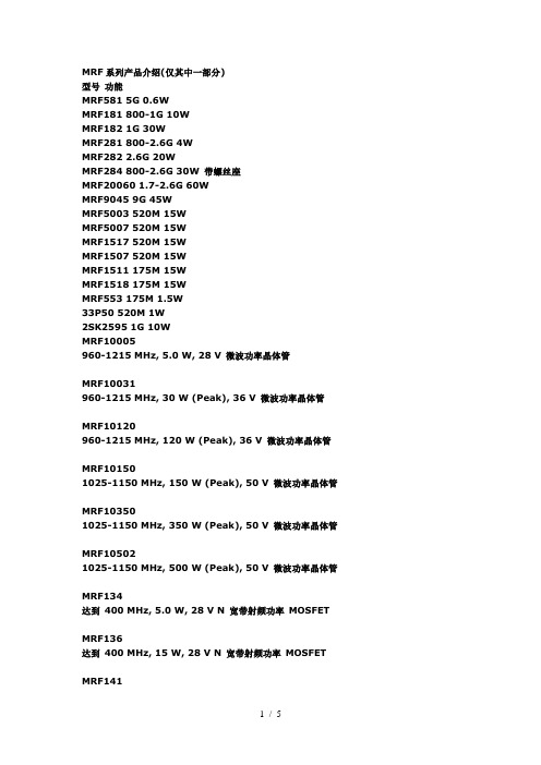
MRF系列产品介绍(仅其中一部分)型号功能MRF581 5G 0.6WMRF181 800-1G 10WMRF182 1G 30WMRF281 800-2.6G 4WMRF282 2.6G 20WMRF284 800-2.6G 30W 带螺丝座MRF20060 1.7-2.6G 60WMRF9045 9G 45WMRF5003 520M 15WMRF5007 520M 15WMRF1517 520M 15WMRF1507 520M 15WMRF1511 175M 15WMRF1518 175M 15WMRF553 175M 1.5W33P50 520M 1W2SK2595 1G 10WMRF10005960-1215 MHz, 5.0 W, 28 V 微波功率晶体管MRF10031960-1215 MHz, 30 W (Peak), 36 V 微波功率晶体管MRF10120960-1215 MHz, 120 W (Peak), 36 V 微波功率晶体管MRF101501025-1150 MHz, 150 W (Peak), 50 V 微波功率晶体管MRF103501025-1150 MHz, 350 W (Peak), 50 V 微波功率晶体管MRF105021025-1150 MHz, 500 W (Peak), 50 V 微波功率晶体管MRF134达到400 MHz, 5.0 W, 28 V N 宽带射频功率MOSFETMRF136达到400 MHz, 15 W, 28 V N 宽带射频功率MOSFET MRF141175 MHz, 150 W, 28 V N 宽带射频功率MOSFETMRF141G175 MHz, 300 W, 28 V N 宽带射频功率MOSFETMRF148A达到175 MHz, 30 W, 50 V N 宽带射频功率MOSFETMRF150达到150 MHz, 150 W, 50 V N 宽带射频功率MOSFETMRF151175 MHz, 150 W, 50 V N 宽带射频功率MOSFETMRF151G175 MHz, 300 W, 50 V N 宽带射频功率MOSFETMRF15480 MHz, 600 W, 50 V N 宽带射频功率MOSFETMRF157达到80 MHz, 600 W, 50 V N 宽带射频功率MOSFETMRF158达到500 MHz, 2.0 W, 28 V TMOS N 宽带射频功率FETMRF160500 MHz, 4.0 W, 28 V N 宽带射频功率MOSFETMRF160061.6 GHz, 6.0 W, 28 V 射频功率晶体管MRF160301.6 GHz, 30 W, 28 V RF 射频功率晶体管MRF166C500 MHz, 20 W, 28 V N 宽带射频功率MOSFETMRF166W500 MHz, 40 W, 28 V TMOS N宽带射频功率FETMRF171A150 MHz, 45 W, 28 V N 宽带射频功率MOSFETMRF173175 MHz, 80 W, 28 V N 宽带射频功率MOSFETMRF174200 MHz, 125 W, 28 V N 宽带射频功率MOSFETMRF177400 MHz, 100 W, 28 V N 宽带射频功率MOSFETMRF275G100–500 MHz, 150 W, 28 V N 宽带射频功率MOSFETMRF275L500 MHz, 100 W, 28 V N 宽带射频功率MOSFETMRF42630 MHz, 25 W, 28 V 射频功率晶体管NPN SiMRF587500 MHz, 15 V, NF = 3.0 dB, 高频晶体管MRFIC1818 1.7-1.9G 2WMRF183 1G 45WMRF187 800-960MHz 85WMRF7042 900MHz 45WMRF175 400MHz 200WMRF581 5G 0.6W2SK2596 800-960MHz 1.5WBFG10 25G 0.6VBFG21 18G 4.5V 0.5A 0.6WBFG403 17G 4.5V 16MA 0.3WBFG410 22G 4.5V 12MA 135MWBFG425 25G 4.5V 30MA 135MWBFG450 45G 0.2WBFG540 45G 3V 30MA 135MWBFG541 9G 0.6WBLT81 800-960M 1.2WTP3022 800-960M 15WTDA1576 ICSRF7062 800-960M 150WMHL9236 800-960M 3WMHL7008 800-960M 3WMHL9128 800-960M 3WATF10136 4G 0.4WCMM2308 800-2.7G 1WCMM1330 1.7-1.9G 2WPF0030 860-915M 7W终端负载50欧5W 3G,18G 驻波小于1.06高频电阻50欧100欧30W 100W 3G型号技术指标数量单价(US$) 型号技术指标数量单价(US$)MRF281 800-2.6G 4W 4K 10 BFG10 25G 0.6W 10K 1MRF282 800-2.6G 10W 4K 15 BFG21 18G 4.5V 0.5A 0.6W 5K 1MRF284 800-2.6G 30W 带螺丝座4K 20 BFG403 17G 4.5V 16MA 0.3W 5K 0.5 MRF20060 1.7-2.6G 60W 6K 30 BFG410 22G 4.5V 12MA 135MW 5K 0.5 MRF181 800-960M 10W 2K 10 BFG425 25G 4.5V 30MA 135MW 4K 0.5 MRF182 1G 30W 500PC 15 BFG450 45G 0.2W 1K 3MRFIC1818 1.7-1.9G 2W 2K 10 BFG540 45G 3V 30MA 135MW 2K 3MRF187 800-960M 85W 1K 30 BFG541 9G 0.6W 3K 0.5MRF7042 900M 45W 2K 15 BFG198 9G 1W 3K 0.5MRF9045 9G 45W 200PC 30 TP3022 800-960M 15W 4K 6MRF581 5G 0.6W 5K 0.5 TDA1576 IC 2K 2MRF5003 520M 15W 5K 3 SRF7062 800-960M 150W 2K 40MRF5007 520M 15W 5K 5 MHL9236 800-960M 3W 200PC 20MRF1517 520M 15W 2K 5 MHL7008 800-960M 3W 500PC 15MRF1507 520M 15W 2K 5 MHL9128 800-960M 3W 500PC 15MRF1511 175M 15W 2K 5 ATF10136 4G 0.4W 10K 1.5MRF1518 175M 15W 1K 5 CMM2308 800-2.7G 1W 10K 1.5MRF553 175M 1.5W 6K 0.5 CMM1330 1.7-1.9G 2W 5K 2MRF137 225MHz 30W 100PC 20 RF2125 1.5-2.2G 1W 1K 5MRF141 225MHZ 150W 100PC 40 PF0030 860-915M 7W 2K 2MRF151G 175MHz 300W 500PC 100 2SC1971 175MHz 7W 5K 1MRF154 150MHz 600W 500PC 200 2SC3356 6.5G 0.2W 5K 0.1MRF175G 500MHz 150W 500PC 100 2SC3357 6.5G 2W 5K 0.2MRF6404 1.8-2G 1K 10 2SC2407 500MHz 0.6W 10K 0.2BLT50 500M 1.2W 5K 0.6 2SC1906 1G 150MW 10K 0.05BLT81 400-960M 1.2W 3K 1 BLU98 5G 0.7W 5K 0.52SK2596 800-960M 1.5W 5K 0.5 33P55 800-960MHz 60W 5K 102SK2595 800-960M 10W 10K 3 E626 800-960Mhz 60W 5K 103SK228 1G 高放双栅管5K 0.15 终端负载50欧5W 3G,18G 驻波小于1.06 3K 10,100温补晶体12.8MHZ 贴片7x7M 5k 3 高频电阻50欧100欧30W 100W 3G 10k 2 MRF92822A 7W 手持对讲机/长距离无绳电话/车载台/手机专用功率发射晶体管集成电路ICMC3361 10K 0.1 HT9200 5K 0.2MC33110 5K 0.2 HT9170 5K 0.2MC34119 5K 0.1 93C66 5K 0.1LM386 5K 0.1 24C08 5K 0.2M54958 5K 1.5 EM92547 5K 0.2M64082 5K 0.5 KA4588 5K 0.1TB31202 5K 0.4 KA567 5K 0.1手机功放及常用元件型号技术指标数量单价(US$) 型号技术指标数量单价(US$)MRFIC0913 800-1000MHZ 2W 现货面议AP109 900MHZ 2W 现货面议27E31 900MHZ 2W 现货面议AP119 1800MHZ 2W 现货面议08K38 900MHZ 2W 现货面议4370451 900MHZ 2W 现货面议08K40 900MHZ 2W 现货面议4370453 1800MHZ 2W 现货面议08K07 900MHZ 2W 现货面议TRF6053 900MHZ 2W 现货面议08K11 900MHZ 2W 现货面议TRF2253 频率合成IC 现货面议PF01420B 900MHZ 2W 现货面议13MHZ 温补晶体现货面议PF01412A 1800MHZ 2W 现货面议881-942 声表滤波器现货面议PF01411B 900MHZ 2W 现货面议PF014110B 1800MHZ 2W 现货面议常用元件MRF5711 8G 0.33W 现货面议BFQ67 8G 0.3W 现货面议MRF5811 5G 0.7W 现货面议BFG540 9G 0.4W 现货面议MMBR941 8G 0.25W 现货面议BFR182W 8G 0.3W 现货面议MMBR503 1G 0.3W 现货面议BFR91 6G 0.3W 现货面议MMBR901 4G 0.3W 现货面议BU508 现货面议84UD22182EB-9C 现货面议Y759B 现货面议F741529AGHH 现货面议08122B 现货面议TWL3011GGM 现货面议089711747 现货面议LMST 现货面议LS28 现货面议。


RF Power Field Effect TransistorsN-Channel Enhancement-Mode Lateral MOSFETsDesigned for broadband commercial and industrial applications withfrequencies up to 1000 MHz. The high gain and broadband performance ofthese devices make them ideal for large-signal, common-source amplifierapplications in 28 volt base station equipment.•Typical Single-Carrier N-CDMA Performance @ 880 MHz, V DD = 28 Volts,I DQ = 350 mA, P out = 10 Watts Avg., IS-95 CDMA (Pilot, Sync, Paging,Traffic Codes 8 Through 13) Channel Bandwidth = 1.2288 MHz. PAR =9.8 dB @ 0.01% Probability on CCDF.Power Gain — 22.7 dBDrain Efficiency — 32%ACPR @ 750 kHz Offset — -47 dBc @ 30 kHz BandwidthGSM EDGE Application•Typical GSM EDGE Performance: V DD = 28 Volts, I DQ = 350 mA,P out = 16 Watts Avg., Full Frequency Band (921-960 MHz)Power Gain — 20 dBDrain Efficiency — 46%Spectral Regrowth @ 400 kHz Offset = -62 dBcSpectral Regrowth @ 600 kHz Offset = -78 dBcEVM — 1.5% rmsGSM Application•Typical GSM Performance: V DD = 28 Volts, I DQ = 350 mA, P out = 45 Watts,Full Frequency Band (921-960 MHz)Power Gain — 20 dBDrain Efficiency — 68%•Capable of Handling 5:1 VSWR, @ 28 Vdc, 880 MHz, 45 Watts CWOutput Power•Characterized with Series Equivalent Large-Signal Impedance Parameters•Integrated ESD Protection•N Suffix Indicates Lead-Free Terminations•200°C Capable Plastic Package•TO-270-2 in Tape and Reel. R1 Suffix = 500 Units per 24 mm,13 inch Reel.•TO-272-2 in Tape and Reel. R1 Suffix = 500 Units per 44 mm,13 inch Reel.Table 1. Maximum RatingsRating Symbol Value Unit Drain-Source Voltage V DSS -0.5, +68Vdc Gate-Source Voltage V GS -0.5, +12Vdc Total Device Dissipation @ T C = 25°CDerate above 25°CP D1751.0WW/°C Storage Temperature Range T stg-65 to +150°C Operating Junction Temperature T J200°CDocument Number: MRF6S9045Rev. 1, 6/2005 Freescale SemiconductorTechnical DataMRF6S9045NR1MRF6S9045NBR1MRF6S9045MR1MRF6S9045MBR12RF Device DataFreescale SemiconductorMRF6S9045NR1 MRF6S9045NBR1 MRF6S9045MR1 MRF6S9045MBR1Table 2. Thermal CharacteristicsCharacteristicSymbol Value (1,2)Unit Thermal Resistance, Junction to Case Case Temperature 81°C, 45 W CW Case Temperature 79°C, 10 W CWR θJC1.01.1°C/WTable 3. ESD Protection CharacteristicsTest MethodologyClass Human Body Model (per JESD22-A114)1A (Minimum)Machine Model (per EIA/JESD22-A115) A (Minimum)Charge Device Model (per JESD22-C101)IV (Minimum)Table 4. Moisture Sensitivity LevelTest MethodologyRating Package Peak TemperatureUnit Per JESD 22-A113, IPC/JEDEC J-STD-0203260°CTable 5. Electrical Characteristics (T C = 25°C unless otherwise noted)CharacteristicSymbolMinTypMaxUnitOff CharacteristicsZero Gate Voltage Drain Leakage Current (V DS = 68 Vdc, V GS = 0 Vdc)I DSS ——10µAdc Zero Gate Voltage Drain Leakage Current (V DS = 28 Vdc, V GS = 0 Vdc)I DSS ——1µAdc Gate-Source Leakage Current (V GS = 5 Vdc, V DS = 0 Vdc)I GSS——1µAdcOn CharacteristicsGate Threshold Voltage(V DS = 10 Vdc, I D = 200 µA)V GS(th)123Vdc Gate Quiescent Voltage(V DS = 28 Vdc, I D = 350 mAdc)V GS(Q)2 2.94Vdc Drain-Source On-Voltage(V GS = 10 Vdc, I D = 1.0 Adc)V DS(on)—0.220.3Vdc Forward Transconductance (V DS = 10 Vdc, I D = 3 Adc)g fs—4—SDynamic CharacteristicsInput Capacitance(V DS = 28 Vdc ± 30 mV(rms)ac @ 1 MHz, V GS = 0 Vdc)C iss —77—pF Output Capacitance(V DS = 28 Vdc ± 30 mV(rms)ac @ 1 MHz, V GS = 0 Vdc)C oss —27—pF Reverse Transfer Capacitance(V DS = 28 Vdc ± 30 mV(rms)ac @ 1 MHz, V GS = 0 Vdc)C rss—0.78—pFFunctional Tests (In Freescale Test Fixture, 50 ohm system) V DD = 28 Vdc, I DQ = 350 mA, P out = 10 W Avg., f = 880 MHz, Single-Carrier N-CDMA, 1.2288 MHz Channel Bandwidth Carrier. ACPR measured in 30 kHz Channel Bandwidth @ ±750 kHz Offset. PAR = 9.8 dB @ 0.01% Probability on CCDF Power Gain G ps 2122.725dB Drain EfficiencyηD 30.532—%Adjacent Channel Power Ratio ACPR —-47-45dBc Input Return LossMRF6S9045NR1(MR1)MRF6S9045NBR1(MBR1)IRL—-20-20-9-7dB1.MTTF calculator available at /rf. Select Tools/Software/Application Software/Calculators to access the MTTF calculators by product.2.Refer to AN1955, Thermal Measurement Methodology of RF Power Amplifiers. Go to /rf. Select Documentation/Application Notes - AN1955.MRF6S9045NR1 MRF6S9045NBR1 MRF6S9045MR1 MRF6S9045MBR13RF Device DataFreescale SemiconductorTable 5. Electrical Characteristics (T C = 25°C unless otherwise noted) (continued)CharacteristicSymbolMinTypMaxUnitTypical GSM EDGE Performances (In Freescale GSM EDGE Test Fixture Optimized for 921-960 MHz, 50 οhm system) V DD = 28 Vdc, I DQ = 350 mA, P out = 16 W Avg., f = 921-960 MHz, GSM EDGE Signal Power Gain G ps —20—dB Drain Efficiency ηD —46—%Error Vector MagnitudeEVM — 1.5—%Spectral Regrowth at 400 kHz Offset SR1—-62—dBc Spectral Regrowth at 600 kHz OffsetSR2—-78—dBcTypical CW Performances (In Freescale GSM Test Fixture Optimized for 921-960 MHz, 50 οhm system) V DD = 28 Vdc, I DQ = 350 mA, P out = 45 W, f = 921-960 MHz Power Gain G ps —20—dB Drain Efficiency ηD —68—%Input Return LossIRL —-12—dB P out @ 1 dB Compression Point (f = 940 MHz)P1dB—52—W4RF Device DataFreescale SemiconductorMRF6S9045NR1 MRF6S9045NBR1 MRF6S9045MR1 MRF6S9045MBR1Figure 1. MRF6S9045NR1(MR1)/NBR1(MBR1) Test Circuit SchematicZ100.360″ x 0.270″ Microstrip Z110.063″ x 0.270″ Microstrip Z120.360″ x 0.065″ Microstrip Z130.095″ x 0.065″ Microstrip Z140.800″ x 0.065″ Microstrip Z150.260″ x 0.065″ Microstrip Z160.325″ x 0.065″ MicrostripPCBTaconic RF-35 0.030″, εr = 3.5Z10.215″ x 0.065″ MicrostripZ20.221″ x 0.065″ Microstrip Z30.500″ x 0.100″ Microstrip Z40.460″ x 0.270″ Microstrip Z50.040″ x 0.270″ MicrostripZ60.280″ x 0.270″ x 0.530″Taper Z70.087″ x 0.525″ Microstrip Z80.435″ x 0.525″ Microstrip Z90.057″ x 0.525″ MicrostripTable 6. MRF6S9045NR1(MR1)/NBR1(MBR1) Test Circuit Component Designations and ValuesPartDescriptionPart NumberManufacturer B1Ferrite Bead 2743019447Fair Rite B2Ferrite Bead2743021447Fair Rite C1, C7, C10, C1447 pF Chip Capacitors100B470JP500X ATC C2, C4, C120.8-8.0 pF Variable Capacitors, Gigatrim 27291SL Johanson C315 pF Chip Capacitor 100B150JP500X ATC C5, C612 pF Chip Capacitors 100B120JP500X ATC C8, C913 pF Chip Capacitors 100B130JP500X ATC C117.5 pF Chip Capacitor100B7R5JP500X ATC C130.6-4.5 pF Variable Capacitor, Gigatrim 27271SLJohanson C15, C16, C1710 µF, 35 V Tantalum Capacitors T491D106K035AS Kemet C18220 µF, 50 V Electrolytic Capacitor 678D227M025CG3D Vishay L1, L212.5 nH Inductor A04T-5Coilcraft R1 1 k Ω Chip Resistor CRCW12061001F100Vishay Dale R2560 k Ω Chip Resistor CRCW12065603F100Vishay Dale R312 Ω Chip ResistorCRC120612R0F100Vishay DaleMRF6S9045NR1 MRF6S9045NBR1 MRF6S9045MR1 MRF6S9045MBR15RF Device DataFreescale SemiconductorFigure 2. MRF6S9045NR1(MR1)/NBR1(MBR1) Test Circuit Component Layout6RF Device DataFreescale SemiconductorMRF6S9045NR1 MRF6S9045NBR1 MRF6S9045MR1 MRF6S9045MBR1TYPICAL CHARACTERISTICSFigure 5. Two-Tone Power Gain versusOutput Power 1001924P out , OUTPUT POWER (WATTS) PEP222010G p s , P O W E R G A I N (d B )23211300Figure 6. Third Order Intermodulation Distortionversus Output Power1P out , OUTPUT POWER (WATTS) PEP101000.5MRF6S9045NR1 MRF6S9045NBR1 MRF6S9045MR1 MRF6S9045MBR17RF Device DataFreescale SemiconductorTYPICAL CHARACTERISTICSFigure 7. Intermodulation Distortion Productsversus Output Power10−80−10P out , OUTPUT POWER (WATTS) PEP−20−30−401100I M D , I N T E R M O D U L A T I O N D I S T O R T I O N (d B c )−50−60−70Figure 8. Intermodulation Distortion Productsversus Tone Spacing10−7000.05TWO−TONE SPACING (MHz)−10−20−30−40−50−601100I M D , I N T E R M O D U L A T I O N D I S T O R T I O N (d B c )0.1Figure 9. Pulse CW Output Power versusInput Power3354P in , INPUT POWER (dBm)525048442426252827312953495147303223P o u t , O U T P U T P O W E R (d B m )4645Figure 10. Single-Carrier N-CDMA ACPR, ALT1, PowerGain and Drain Efficiency versus Output Power0−85P out , OUTPUT POWER (WATTS) AVG.60−2550−3540−4530−5510−75110−6520ηD , D R A I N E F F I C I E N C Y (%), G p s , P O W E R G A I N (d B )A L T 1, C H A N N E L P O W E R (dB c )A C P R , A D J A C E N T C H A N N E L P O W E R R A T I O (dB c )508RF Device DataFreescale SemiconductorMRF6S9045NR1 MRF6S9045NBR1 MRF6S9045MR1 MRF6S9045MBR1TYPICAL CHARACTERISTICS2423222018ηD , D R A I N E F F I C I E N C Y (%)G p s , P O W E R G A I N (d B )G p s , P O W E R G A I N (d B )2119171621010T J , JUNCTION TEMPERATURE (°C)This above graph displays calculated MTTF in hours x ampere 2drain current. Life tests at elevated temperatures have correlated to better than ±10% of the theoretical prediction for metal failure. Divide MTTF factor by I D 2 for MTTF in a particular application.101010M T T F F A C T O R (H O U R S X A M P S 2)90110130150170190Figure 13. MTTF Factor versus Junction Temperature100120140160180200MRF6S9045NR1 MRF6S9045NBR1 MRF6S9045MR1 MRF6S9045MBR19RF Device DataFreescale SemiconductorN-CDMA TEST SIGNAL100.00011000PEAK −TO−AVERAGE (dB)Figure 14. Single-Carrier CCDF N-CDMA1010.10.010.0012468P R O B A B I L I T Y (%)−60−110−10(d B )−20−30−40−50−70−80−90−1002.90.7 2.21.50−0.7−1.5−2.2−2.9−3.6 3.6f, FREQUENCY (MHz)Figure 15. Single-Carrier N-CDMA Spectrum10RF Device DataFreescale SemiconductorMRF6S9045NR1 MRF6S9045NBR1 MRF6S9045MR1 MRF6S9045MBR1Figure 16. Series Equivalent Source and Load Impedancef MHz Z sourceΩZ load Ω850865880 3.05 + j1.273.31 + j1.333.16 + j1.330.42 + j0.300.42 + j0.440.45 + j0.60V DD = 28 Vdc, I DQ = 350 mA, P out = 10 W Avg.8959103.35 + j1.053.43 + j1.200.48 + j0.740.50 + j0.85Z source =Test circuit impedance as measured fromgate to ground.Zload=Test circuit impedance as measured from drain to ground.ZsourceZloadOutput Matching NetworkZ o = 5 ΩZ sourcef = 850 MHzf = 910 MHzZ loadf = 910 MHzf = 850 MHzMRF6S9045NR1 MRF6S9045NBR1 MRF6S9045MR1 MRF6S9045MBR111RF Device DataFreescale SemiconductorNOTES12RF Device Data Freescale SemiconductorMRF6S9045NR1 MRF6S9045NBR1 MRF6S9045MR1 MRF6S9045MBR1NOTESMRF6S9045NR1 MRF6S9045NBR1 MRF6S9045MR1 MRF6S9045MBR113RF Device DataFreescale SemiconductorNOTES14RF Device DataFreescale SemiconductorMRF6S9045NR1 MRF6S9045NBR1 MRF6S9045MR1 MRF6S9045MBR1PACKAGE DIMENSIONSTO-270-2PLASTICCASE 1265-08ISSUE HMRF6S9045NR1(MR1)MRF6S9045NR1 MRF6S9045NBR1 MRF6S9045MR1 MRF6S9045MBR115RF Device DataFreescale SemiconductorCASE 1337-03ISSUE C AREA OF THE HEAT SLUG.DIM A MIN MAX MIN MAX MILLIMETERS .100.104 2.54 2.64INCHES A1.039.0430.99 1.09A2.040.042 1.02 1.07D .928.93223.5723.67D1E .438.44211.1211.23E1.248.252 6.30 6.40F b1.193c1.007.011.18r1.063.0681.60aaa1.810 BSC .00420.57 BSC .10STYLE 1:PIN 1.DRAIN2.GATE3.SOURCE.025 BSC .281.73.199 4.900.64 BSC5.05E2.241.2456.12 6.22TO-272-2PLASTICMRF6S9045NBR1(MBR1)Information in this document is provided solely to enable system and softwareimplementers to use Freescale Semiconductor products. There are no express orimplied copyright licenses granted hereunder to design or fabricate any integratedcircuits or integrated circuits based on the information in this document.Freescale Semiconductor reserves the right to make changes without further notice toany products herein. Freescale Semiconductor makes no warranty, representation orguarantee regarding the suitability of its products for any particular purpose, nor doesFreescale Semiconductor assume any liability arising out of the application or use ofany product or circuit, and specifically disclaims any and all liability, including withoutlimitation consequential or incidental damages. “Typical” parameters that may beprovided in Freescale Semiconductor data sheets and/or specifications can and dovary in different applications and actual performance may vary over time. All operatingparameters, including “Typicals”, must be validated for each customer application bycustomer’s technical experts. Freescale Semiconductor does not convey any licenseunder its patent rights nor the rights of others. Freescale Semiconductor products arenot designed, intended, or authorized for use as components in systems intended forsurgical implant into the body, or other applications intended to support or sustain life,or for any other application in which the failure of the Freescale Semiconductor productcould create a situation where personal injury or death may occur. Should Buyerpurchase or use Freescale Semiconductor products for any such unintended orunauthorized application, Buyer shall indemnify and hold Freescale Semiconductorand its officers, employees, subsidiaries, affiliates, and distributors harmless against allclaims, costs, damages, and expenses, and reasonable attorney fees arising out of,directly or indirectly, any claim of personal injury or death associated with suchunintended or unauthorized use, even if such claim alleges that FreescaleSemiconductor was negligent regarding the design or manufacture of the part.Freescale t and the Freescale logo are trademarks of Freescale Semiconductor, Inc.All other product or service names are the property of their respective owners.Freescale Semiconductor, Inc. 2005. All rights reserved.How to Reach Us:Home Page:E-mail:support@USA/Europe or Locations Not Listed:Freescale SemiconductorTechnical Information Center, CH3701300 N. Alma School RoadChandler, Arizona 85224+1-800-521-6274 or +1-480-768-2130support@Europe, Middle East, and Africa:Freescale Halbleiter Deutschland GmbHTechnical Information CenterSchatzbogen 781829 Muenchen, Germany+44 1296 380 456 (English)+46 8 52200080 (English)+49 89 92103 559 (German)+33 1 69 35 48 48 (French)support@Japan:Freescale Semiconductor Japan Ltd.HeadquartersARCO Tower 15F1-8-1, Shimo-Meguro, Meguro-ku,Tokyo 153-0064Japan0120 191014 or +81 3 5437 9125support.japan@Asia/Pacific:Freescale Semiconductor Hong Kong Ltd.Technical Information Center2 Dai King StreetTai Po Industrial EstateTai Po, N.T., Hong Kong+800 2666 8080@For Literature Requests Only:Freescale Semiconductor Literature Distribution CenterP.O. Box 5405Denver, Colorado 802171-800-441-2447 or 303-675-2140Fax: 303-675-2150LDCForFreescaleSemiconductor@。