1/231
PRELIMINARY DATA
January 2005This is preliminary information on a new product now in development or undergoing evaluation. Details are subject to change without notice.
uPSD33xx
Turbo Series
Fast 8032 MCU with Programmable Logic
FEATURES SUMMARY
■
FAST 8-BIT TURBO 8032 MCU, 40MHz –Advanced core, 4-clocks per instruction –10 MIPs peak performance at 40MHz (5V)–JTAG Debug and In-System
Programming
–Branch Cache & 6 instruction Prefetch
Queue
–Dual XDATA pointers with auto incr & decr –Compatible with 3rd party 8051 tools ■
DUAL FLASH MEMORIES WITH MEMORY MANAGEMENT
–Place either memory into 8032 program
address space or data address space –READ-while-WRITE operation for In-Application Programming and EEPROM emulation
–Single voltage program and erase
–100K guaranteed erase cycles, 15-year
retention
■
CLOCK, RESET, AND SUPPLY MANAGEMENT
–SRAM is Battery Backup capable
–Flexible 8-level CPU clock divider register –Normal, Idle, and Power Down Modes –Power-on and Low Voltage reset
supervisor
–Programmable Watchdog Timer ■
PROGRAMMABLE LOGIC, GENERAL PURPOSE
–16 macrocells
–Create shifters, state machines, chip-selects, glue-logic to keypads, panels, LCDs, others
■
COMMUNICATION INTERFACES
–I 2C Master/Slave controller, 833KHz –SPI Master controller, 10MHz
–Two UARTs with independent baud rate –IrDA protocol support up to 115K baud –Up to 46 I/O, 5V tolerant on 3.3V
uPSD33xxV
■
A/D CONVERTER
–Eight Channels, 10-bit resolution, 6μs ■
TIMERS AND INTERRUPTS
–Three 8032 standard 16-bit timers
–Programmable Counter Array (PCA), six
16-bit modules for PWM, CAPCOM, and timers
–8/10/16-bit PWM operation
–11 Interrupt sources with two external
interrupt pins
■
OPERATING VOLTAGE SOURCE (±10%)–5V devices use both 5.0V and 3.3V
sources
– 3.3V devices use only 3.3V source
uPSD33xx
2/231
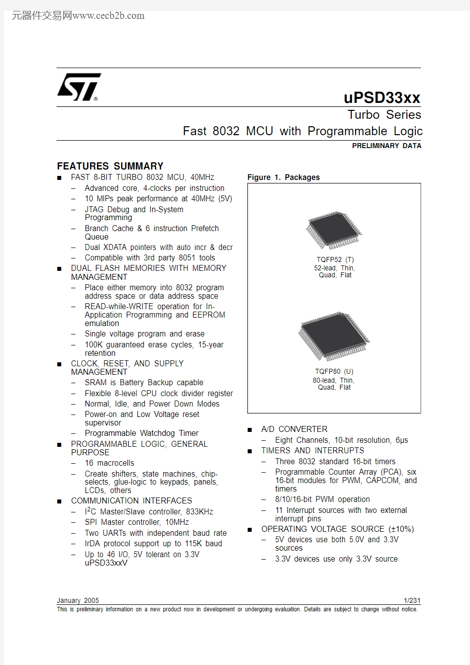
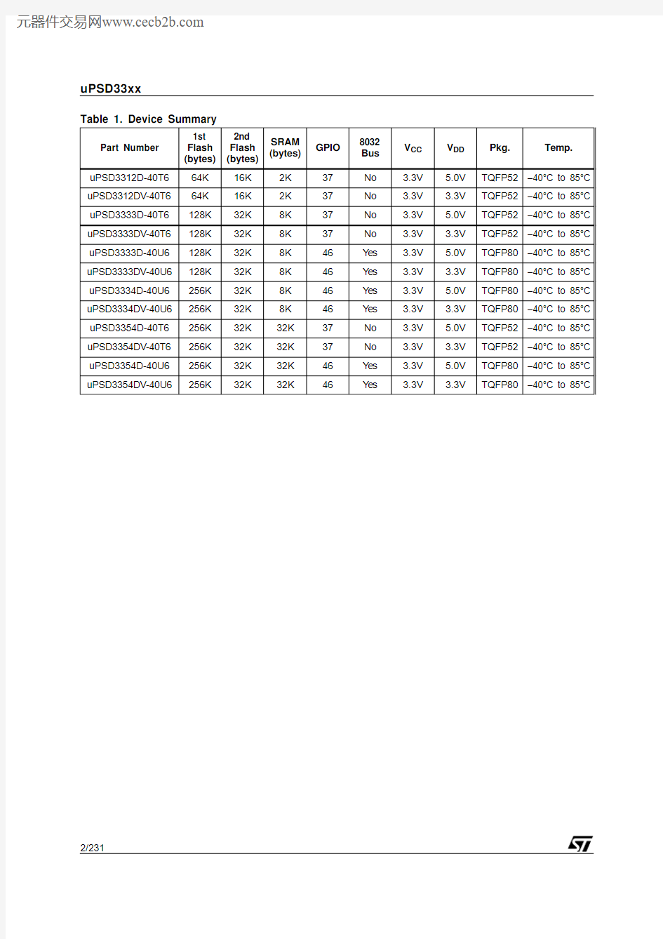
Table 1. Device Summary
Part Number 1st Flash (bytes)2nd Flash (bytes)SRAM (bytes)GPIO 8032 Bus V CC V DD Pkg.
Temp.
uPSD3312D-40T664K 16K 2K 37No 3.3V 5.0V TQFP52–40°C to 85°C uPSD3312DV-40T664K 16K 2K 37No 3.3V 3.3V TQFP52–40°C to 85°C uPSD3333D-40T6128K 32K 8K 37No 3.3V 5.0V TQFP52–40°C to 85°C uPSD3333DV-40T6128K 32K 8K 37No 3.3V 3.3V TQFP52–40°C to 85°C uPSD3333D-40U6128K 32K 8K 46Yes 3.3V 5.0V TQFP80–40°C to 85°C uPSD3333DV-40U6128K 32K 8K 46Yes 3.3V 3.3V TQFP80–40°C to 85°C uPSD3334D-40U6256K 32K 8K 46Yes 3.3V 5.0V TQFP80–40°C to 85°C uPSD3334DV-40U6256K 32K 8K 46Yes 3.3V 3.3V TQFP80–40°C to 85°C uPSD3354D-40T6256K 32K 32K 37No 3.3V 5.0V TQFP52–40°C to 85°C uPSD3354DV-40T6256K 32K 32K 37No 3.3V 3.3V TQFP52–40°C to 85°C uPSD3354D-40U6256K 32K 32K 46Yes 3.3V 5.0V TQFP80–40°C to 85°C uPSD3354DV-40U6
256K
32K
32K
46
Yes
3.3V
3.3V
TQFP80–40°C to 85°C
uPSD33xx TABLE OF CONTENTS
FEATURES SUMMARY . . . . . . . . . . . . . . . . . . . . . . . . . . . . . . . . . . . . . . . . . . . . . . . . . . . . . . . . . . . . .1
SUMMARY DESCRIPTION. . . . . . . . . . . . . . . . . . . . . . . . . . . . . . . . . . . . . . . . . . . . . . . . . . . . . . . . . . .7 PIN DESCRIPTIONS. . . . . . . . . . . . . . . . . . . . . . . . . . . . . . . . . . . . . . . . . . . . . . . . . . . . . . . . . . . . . . . .8 uPSD33xx HARDWARE DESCRIPTION. . . . . . . . . . . . . . . . . . . . . . . . . . . . . . . . . . . . . . . . . . . . . . .13
MEMORY ORGANIZATION . . . . . . . . . . . . . . . . . . . . . . . . . . . . . . . . . . . . . . . . . . . . . . . . . . . . . . . . .15
Internal Memory (MCU Module, Standard 8032 Memory: DATA, IDATA, SFR) . . . . . . . . . . . .16 External Memory (PSD Module: Program memory, Data memory). . . . . . . . . . . . . . . . . . . . . .16
8032 MCU CORE PERFORMANCE ENHANCEMENTS . . . . . . . . . . . . . . . . . . . . . . . . . . . . . . . . . . .17
Pre-Fetch Queue (PFQ) and Branch Cache (BC) . . . . . . . . . . . . . . . . . . . . . . . . . . . . . . . . . . . .19 PFQ Example, Multi-cycle Instructions. . . . . . . . . . . . . . . . . . . . . . . . . . . . . . . . . . . . . . . . . . . .19 Aggregate Performance . . . . . . . . . . . . . . . . . . . . . . . . . . . . . . . . . . . . . . . . . . . . . . . . . . . . . . . .19
MCU MODULE DISCRIPTION . . . . . . . . . . . . . . . . . . . . . . . . . . . . . . . . . . . . . . . . . . . . . . . . . . . . . . .21
8032 MCU REGISTERS . . . . . . . . . . . . . . . . . . . . . . . . . . . . . . . . . . . . . . . . . . . . . . . . . . . . . . . . . . . .21
Stack Pointer (SP). . . . . . . . . . . . . . . . . . . . . . . . . . . . . . . . . . . . . . . . . . . . . . . . . . . . . . . . . . . . .21 Data Pointer (DPTR) . . . . . . . . . . . . . . . . . . . . . . . . . . . . . . . . . . . . . . . . . . . . . . . . . . . . . . . . . . .21 Program Counter (PC). . . . . . . . . . . . . . . . . . . . . . . . . . . . . . . . . . . . . . . . . . . . . . . . . . . . . . . . . .21 Accumulator (ACC). . . . . . . . . . . . . . . . . . . . . . . . . . . . . . . . . . . . . . . . . . . . . . . . . . . . . . . . . . . .21
B Register (B). . . . . . . . . . . . . . . . . . . . . . . . . . . . . . . . . . . . . . . . . . . . . . . . . . . . . . . . . . . . . . . . .21
General Purpose Registers (R0 - R7). . . . . . . . . . . . . . . . . . . . . . . . . . . . . . . . . . . . . . . . . . . . . .22 Program Status Word (PSW) . . . . . . . . . . . . . . . . . . . . . . . . . . . . . . . . . . . . . . . . . . . . . . . . . . . .22
SPECIAL FUNCTION REGISTERS (SFR). . . . . . . . . . . . . . . . . . . . . . . . . . . . . . . . . . . . . . . . . . . . . .23
8032 ADDRESSING MODES . . . . . . . . . . . . . . . . . . . . . . . . . . . . . . . . . . . . . . . . . . . . . . . . . . . . . . . .30
Register Addressing. . . . . . . . . . . . . . . . . . . . . . . . . . . . . . . . . . . . . . . . . . . . . . . . . . . . . . . . . . .30 Direct Addressing . . . . . . . . . . . . . . . . . . . . . . . . . . . . . . . . . . . . . . . . . . . . . . . . . . . . . . . . . . . . .30 Register Indirect Addressing. . . . . . . . . . . . . . . . . . . . . . . . . . . . . . . . . . . . . . . . . . . . . . . . . . . .30 Immediate Addressing . . . . . . . . . . . . . . . . . . . . . . . . . . . . . . . . . . . . . . . . . . . . . . . . . . . . . . . . .30 External Direct Addressing . . . . . . . . . . . . . . . . . . . . . . . . . . . . . . . . . . . . . . . . . . . . . . . . . . . . .30 External Indirect Addressing . . . . . . . . . . . . . . . . . . . . . . . . . . . . . . . . . . . . . . . . . . . . . . . . . . . .30 Indexed Addressing . . . . . . . . . . . . . . . . . . . . . . . . . . . . . . . . . . . . . . . . . . . . . . . . . . . . . . . . . . .31 Relative Addressing . . . . . . . . . . . . . . . . . . . . . . . . . . . . . . . . . . . . . . . . . . . . . . . . . . . . . . . . . . .31 Absolute Addressing . . . . . . . . . . . . . . . . . . . . . . . . . . . . . . . . . . . . . . . . . . . . . . . . . . . . . . . . . .31 Long Addressing. . . . . . . . . . . . . . . . . . . . . . . . . . . . . . . . . . . . . . . . . . . . . . . . . . . . . . . . . . . . . .31 Bit Addressing. . . . . . . . . . . . . . . . . . . . . . . . . . . . . . . . . . . . . . . . . . . . . . . . . . . . . . . . . . . . . . . .31
uPSD33xx INSTRUCTION SET SUMMARY . . . . . . . . . . . . . . . . . . . . . . . . . . . . . . . . . . . . . . . . . . . .32
3/231
uPSD33xx
DUAL DATA POINTERS. . . . . . . . . . . . . . . . . . . . . . . . . . . . . . . . . . . . . . . . . . . . . . . . . . . . . . . . . . . .37
Data Pointer Control Register, DPTC (85h). . . . . . . . . . . . . . . . . . . . . . . . . . . . . . . . . . . . . . . . .37 Data Pointer Mode Register, DPTM (86h) . . . . . . . . . . . . . . . . . . . . . . . . . . . . . . . . . . . . . . . . . .38
DEBUG UNIT. . . . . . . . . . . . . . . . . . . . . . . . . . . . . . . . . . . . . . . . . . . . . . . . . . . . . . . . . . . . . . . . . . . . .39
INTERRUPT SYSTEM. . . . . . . . . . . . . . . . . . . . . . . . . . . . . . . . . . . . . . . . . . . . . . . . . . . . . . . . . . . . . .40 Individual Interrupt Sources. . . . . . . . . . . . . . . . . . . . . . . . . . . . . . . . . . . . . . . . . . . . . . . . . . . . .43
MCU CLOCK GENERATION . . . . . . . . . . . . . . . . . . . . . . . . . . . . . . . . . . . . . . . . . . . . . . . . . . . . . . . .46
MCU_CLK. . . . . . . . . . . . . . . . . . . . . . . . . . . . . . . . . . . . . . . . . . . . . . . . . . . . . . . . . . . . . . . . . . . .46 PERIPH_CLK . . . . . . . . . . . . . . . . . . . . . . . . . . . . . . . . . . . . . . . . . . . . . . . . . . . . . . . . . . . . . . . . .46
POWER SAVING MODES . . . . . . . . . . . . . . . . . . . . . . . . . . . . . . . . . . . . . . . . . . . . . . . . . . . . . . . . . .48
Idle Mode . . . . . . . . . . . . . . . . . . . . . . . . . . . . . . . . . . . . . . . . . . . . . . . . . . . . . . . . . . . . . . . . . . . .48 Power-down Mode. . . . . . . . . . . . . . . . . . . . . . . . . . . . . . . . . . . . . . . . . . . . . . . . . . . . . . . . . . . . .48 Reduced Frequency Mode . . . . . . . . . . . . . . . . . . . . . . . . . . . . . . . . . . . . . . . . . . . . . . . . . . . . . .48
OSCILLATOR AND EXTERNAL COMPONENTS . . . . . . . . . . . . . . . . . . . . . . . . . . . . . . . . . . . . . . . .51
I/O PORTS of MCU MODULE. . . . . . . . . . . . . . . . . . . . . . . . . . . . . . . . . . . . . . . . . . . . . . . . . . . . . . . .53 MCU Port Operating Modes . . . . . . . . . . . . . . . . . . . . . . . . . . . . . . . . . . . . . . . . . . . . . . . . . . . . .53
MCU BUS INTERFACE. . . . . . . . . . . . . . . . . . . . . . . . . . . . . . . . . . . . . . . . . . . . . . . . . . . . . . . . . . . . .62
Bus Read Cycles (PSEN or RD). . . . . . . . . . . . . . . . . . . . . . . . . . . . . . . . . . . . . . . . . . . . . . . . . .62 Bus Write Cycles (WR) . . . . . . . . . . . . . . . . . . . . . . . . . . . . . . . . . . . . . . . . . . . . . . . . . . . . . . . . .62 Controlling the PFQ and BC. . . . . . . . . . . . . . . . . . . . . . . . . . . . . . . . . . . . . . . . . . . . . . . . . . . . .62
SUPERVISORY FUNCTIONS. . . . . . . . . . . . . . . . . . . . . . . . . . . . . . . . . . . . . . . . . . . . . . . . . . . . . . . .65
External Reset Input Pin, RESET_IN . . . . . . . . . . . . . . . . . . . . . . . . . . . . . . . . . . . . . . . . . . . . . .65 Low V CC Voltage Detect, LVD. . . . . . . . . . . . . . . . . . . . . . . . . . . . . . . . . . . . . . . . . . . . . . . . . . . .66 Power-up Reset. . . . . . . . . . . . . . . . . . . . . . . . . . . . . . . . . . . . . . . . . . . . . . . . . . . . . . . . . . . . . . .66 JTAG Debug Reset . . . . . . . . . . . . . . . . . . . . . . . . . . . . . . . . . . . . . . . . . . . . . . . . . . . . . . . . . . . .66 Watchdog Timer, WDT . . . . . . . . . . . . . . . . . . . . . . . . . . . . . . . . . . . . . . . . . . . . . . . . . . . . . . . . .66
STANDARD 8032 TIMER/COUNTERS . . . . . . . . . . . . . . . . . . . . . . . . . . . . . . . . . . . . . . . . . . . . . . . .69
Standard Timer SFRs . . . . . . . . . . . . . . . . . . . . . . . . . . . . . . . . . . . . . . . . . . . . . . . . . . . . . . . . . .69 Clock Sources . . . . . . . . . . . . . . . . . . . . . . . . . . . . . . . . . . . . . . . . . . . . . . . . . . . . . . . . . . . . . . . .69 SFR, TCON. . . . . . . . . . . . . . . . . . . . . . . . . . . . . . . . . . . . . . . . . . . . . . . . . . . . . . . . . . . . . . . . . . .71 SFR, TMOD. . . . . . . . . . . . . . . . . . . . . . . . . . . . . . . . . . . . . . . . . . . . . . . . . . . . . . . . . . . . . . . . . . .71 Timer 0 and Timer 1 Operating Modes . . . . . . . . . . . . . . . . . . . . . . . . . . . . . . . . . . . . . . . . . . . .71 Timer 2 . . . . . . . . . . . . . . . . . . . . . . . . . . . . . . . . . . . . . . . . . . . . . . . . . . . . . . . . . . . . . . . . . . . . . .74
SERIAL UART INTERFACES. . . . . . . . . . . . . . . . . . . . . . . . . . . . . . . . . . . . . . . . . . . . . . . . . . . . . . . .81 UART Operation Modes . . . . . . . . . . . . . . . . . . . . . . . . . . . . . . . . . . . . . . . . . . . . . . . . . . . . . . . .81
4/231
uPSD33xx
Serial Port Control Registers. . . . . . . . . . . . . . . . . . . . . . . . . . . . . . . . . . . . . . . . . . . . . . . . . . . .82 UART Baud Rates . . . . . . . . . . . . . . . . . . . . . . . . . . . . . . . . . . . . . . . . . . . . . . . . . . . . . . . . . . . . .84 More About UART Mode 0 . . . . . . . . . . . . . . . . . . . . . . . . . . . . . . . . . . . . . . . . . . . . . . . . . . . . . .85 More About UART Mode 1 . . . . . . . . . . . . . . . . . . . . . . . . . . . . . . . . . . . . . . . . . . . . . . . . . . . . . .87 More About UART Modes 2 and 3 . . . . . . . . . . . . . . . . . . . . . . . . . . . . . . . . . . . . . . . . . . . . . . . .89
IrDA INTERFACE . . . . . . . . . . . . . . . . . . . . . . . . . . . . . . . . . . . . . . . . . . . . . . . . . . . . . . . . . . . . . . . . .92 Pulse Width Selection. . . . . . . . . . . . . . . . . . . . . . . . . . . . . . . . . . . . . . . . . . . . . . . . . . . . . . . . . .94
I2C INTERFACE . . . . . . . . . . . . . . . . . . . . . . . . . . . . . . . . . . . . . . . . . . . . . . . . . . . . . . . . . . . . . . . . . .95
I2C Interface Main Features . . . . . . . . . . . . . . . . . . . . . . . . . . . . . . . . . . . . . . . . . . . . . . . . . . . . .95 Communication Flow . . . . . . . . . . . . . . . . . . . . . . . . . . . . . . . . . . . . . . . . . . . . . . . . . . . . . . . . . .96 Operating Modes. . . . . . . . . . . . . . . . . . . . . . . . . . . . . . . . . . . . . . . . . . . . . . . . . . . . . . . . . . . . . .98 Bus Arbitration . . . . . . . . . . . . . . . . . . . . . . . . . . . . . . . . . . . . . . . . . . . . . . . . . . . . . . . . . . . . . . .98 Clock Synchronization . . . . . . . . . . . . . . . . . . . . . . . . . . . . . . . . . . . . . . . . . . . . . . . . . . . . . . . . .98 General Call Address . . . . . . . . . . . . . . . . . . . . . . . . . . . . . . . . . . . . . . . . . . . . . . . . . . . . . . . . . .98 Serial I/O Engine (SIOE) . . . . . . . . . . . . . . . . . . . . . . . . . . . . . . . . . . . . . . . . . . . . . . . . . . . . . . . .99 I2C Interface Control Register (S1CON) . . . . . . . . . . . . . . . . . . . . . . . . . . . . . . . . . . . . . . . . . .100 I2C Interface Status Register (S1STA). . . . . . . . . . . . . . . . . . . . . . . . . . . . . . . . . . . . . . . . . . . .102 I2C Data Shift Register (S1DAT). . . . . . . . . . . . . . . . . . . . . . . . . . . . . . . . . . . . . . . . . . . . . . . . .104 I2C Address Register (S1ADR). . . . . . . . . . . . . . . . . . . . . . . . . . . . . . . . . . . . . . . . . . . . . . . . . .104 I2C START Sample Setting (S1SETUP) . . . . . . . . . . . . . . . . . . . . . . . . . . . . . . . . . . . . . . . . . . .105 I2C Operating Sequences. . . . . . . . . . . . . . . . . . . . . . . . . . . . . . . . . . . . . . . . . . . . . . . . . . . . . .108
SPI (SYNCHRONOUS PERIPHERAL INTERFACE) . . . . . . . . . . . . . . . . . . . . . . . . . . . . . . . . . . . . .112
SPI Bus Features and Communication Flow . . . . . . . . . . . . . . . . . . . . . . . . . . . . . . . . . . . . . .113 Full-Duplex Operation. . . . . . . . . . . . . . . . . . . . . . . . . . . . . . . . . . . . . . . . . . . . . . . . . . . . . . . . .113 Bus-Level Activity. . . . . . . . . . . . . . . . . . . . . . . . . . . . . . . . . . . . . . . . . . . . . . . . . . . . . . . . . . . .113 SPI SFR Registers. . . . . . . . . . . . . . . . . . . . . . . . . . . . . . . . . . . . . . . . . . . . . . . . . . . . . . . . . . . .115 SPI Configuration . . . . . . . . . . . . . . . . . . . . . . . . . . . . . . . . . . . . . . . . . . . . . . . . . . . . . . . . . . . .116 Dynamic Control . . . . . . . . . . . . . . . . . . . . . . . . . . . . . . . . . . . . . . . . . . . . . . . . . . . . . . . . . . . . .116
ANALOG-TO-DIGITAL CONVERTOR (ADC) . . . . . . . . . . . . . . . . . . . . . . . . . . . . . . . . . . . . . . . . . .120 Port 1 ADC Channel Selects. . . . . . . . . . . . . . . . . . . . . . . . . . . . . . . . . . . . . . . . . . . . . . . . . . . .120
PROGRAMMABLE COUNTER ARRAY (PCA) WITH PWM . . . . . . . . . . . . . . . . . . . . . . . . . . . . . . .123
PCA Block . . . . . . . . . . . . . . . . . . . . . . . . . . . . . . . . . . . . . . . . . . . . . . . . . . . . . . . . . . . . . . . . . .123 PCA Clock Selection. . . . . . . . . . . . . . . . . . . . . . . . . . . . . . . . . . . . . . . . . . . . . . . . . . . . . . . . . .125 Operation of TCM Modes . . . . . . . . . . . . . . . . . . . . . . . . . . . . . . . . . . . . . . . . . . . . . . . . . . . . . .126 Capture Mode. . . . . . . . . . . . . . . . . . . . . . . . . . . . . . . . . . . . . . . . . . . . . . . . . . . . . . . . . . . . . . . .126 Timer Mode . . . . . . . . . . . . . . . . . . . . . . . . . . . . . . . . . . . . . . . . . . . . . . . . . . . . . . . . . . . . . . . . .126 Toggle Mode . . . . . . . . . . . . . . . . . . . . . . . . . . . . . . . . . . . . . . . . . . . . . . . . . . . . . . . . . . . . . . . .126 PWM Mode - (X8), Fixed Frequency. . . . . . . . . . . . . . . . . . . . . . . . . . . . . . . . . . . . . . . . . . . . . .126 PWM Mode - (X8), Programmable Frequency. . . . . . . . . . . . . . . . . . . . . . . . . . . . . . . . . . . . . .128 PWM Mode - Fixed Frequency, 16-bit . . . . . . . . . . . . . . . . . . . . . . . . . . . . . . . . . . . . . . . . . . . .129
5/231
uPSD33xx
PWM Mode - Fixed Frequency, 10-bit . . . . . . . . . . . . . . . . . . . . . . . . . . . . . . . . . . . . . . . . . . . .129 Writing to Capture/Compare Registers. . . . . . . . . . . . . . . . . . . . . . . . . . . . . . . . . . . . . . . . . . .129 Control Register Bit Definition. . . . . . . . . . . . . . . . . . . . . . . . . . . . . . . . . . . . . . . . . . . . . . . . . .129 TCM Interrupts. . . . . . . . . . . . . . . . . . . . . . . . . . . . . . . . . . . . . . . . . . . . . . . . . . . . . . . . . . . . . . .132
PSD MODULE. . . . . . . . . . . . . . . . . . . . . . . . . . . . . . . . . . . . . . . . . . . . . . . . . . . . . . . . . . . . . . . . . . .133
PSD Module Functional Description . . . . . . . . . . . . . . . . . . . . . . . . . . . . . . . . . . . . . . . . . . . . .134 Memory Mapping. . . . . . . . . . . . . . . . . . . . . . . . . . . . . . . . . . . . . . . . . . . . . . . . . . . . . . . . . . . . .138 Runtime Control Register Definitions (csiop). . . . . . . . . . . . . . . . . . . . . . . . . . . . . . . . . . . . . .145 PSD Module Detailed Operation. . . . . . . . . . . . . . . . . . . . . . . . . . . . . . . . . . . . . . . . . . . . . . . . .147 PSD Module Reset Conditions. . . . . . . . . . . . . . . . . . . . . . . . . . . . . . . . . . . . . . . . . . . . . . . . . .193
AC/DC PARAMETERS. . . . . . . . . . . . . . . . . . . . . . . . . . . . . . . . . . . . . . . . . . . . . . . . . . . . . . . . . . . .202 MAXIMUM RATING. . . . . . . . . . . . . . . . . . . . . . . . . . . . . . . . . . . . . . . . . . . . . . . . . . . . . . . . . . . . . . .204 DC AND AC PARAMETERS. . . . . . . . . . . . . . . . . . . . . . . . . . . . . . . . . . . . . . . . . . . . . . . . . . . . . . . .204 PACKAGE MECHANICAL INFORMATION. . . . . . . . . . . . . . . . . . . . . . . . . . . . . . . . . . . . . . . . . . . .225 PART NUMBERING . . . . . . . . . . . . . . . . . . . . . . . . . . . . . . . . . . . . . . . . . . . . . . . . . . . . . . . . . . . . . .229 REVISION HISTORY. . . . . . . . . . . . . . . . . . . . . . . . . . . . . . . . . . . . . . . . . . . . . . . . . . . . . . . . . . . . . .230
6/231
uPSD33xx SUMMARY DESCRIPTION
The Turbo uPSD33xx Series combines a powerful 8051-based microcontroller with a flexible memory structure, programmable logic, and a rich periph-eral mix to form an ideal embedded controller. At its core is a fast 4-cycle 8032 MCU with a 6-byte instruction prefetch queue (PFQ) and a 4-entry ful-ly associative branching cache (BC) to maximize MCU performance, enabling loops of code in smaller localities to execute extremely fast.
Code development is easily managed without a hardware In-Circuit Emulator by using the serial JTAG debug interface. JTAG is also used for In-System Programming (ISP) in as little as 10 sec-onds, perfect for manufacturing and lab develop-ment. The 8032 core is coupled to Programmable System Device (PSD) architecture to optimize the 8032 memory structure, offering two independent banks of Flash memory that can be placed at vir-tually any address within 8032 program or data ad-dress space, and easily paged beyond 64K bytes using on-chip programmable decode logic. Dual Flash memory banks provide a robust solution for remote product updates in the field through In-Ap-plication Programming (IAP). Dual Flash banks also support EEPROM emulation, eliminating the need for external EEPROM chips. General pur-pose programmable logic (PLD) is included to build an endless variety of glue-logic, saving exter-nal logic devices. The PLD is configured using the software development tool, PSDsoft Express, available from the web at https://www.doczj.com/doc/f918909229.html,/psm, at no charge. The uPSD33xx also includes supervisor functions such as a programmable watchdog timer and low-voltage reset.
7/231
uPSD33xx
PIN DESCRIPTIONS
Note: 1.For 5V applications, V DD must be connected to a 5.0V source. For 3.3V applications, V DD must be connected to a 3.3V source.
2.These signals can be used on one of two different ports (Port 1 or Port 4) for flexibility. Default is Port1.
3.V REF and 3.3V AV CC are shared in the 52-pin package only. ADC channels must use AV CC as V REF for the 52-pin package.
8/231
uPSD33xx
Note: 1.For 5V applications, V DD must be connected to a 5.0V source. For 3.3V applications, V DD must be connected to a 3.3V source.
2.These signals can be used on one of two different ports (Port 1 or Port 4) for flexibility. Default is Port1.
9/231
uPSD33xx
10/231
Table 2. Pin Definitions
Port Pin Signal Name 80-Pin No.52-Pin
No.(1)In/Out
Function
Basic
Alternate 1
Alternate 2
MCUAD0AD036N/A I/O External Bus
Multiplexed Address/Data bus A0/D0MCUAD1AD137N/A I/O Multiplexed Address/Data bus A1/D1
MCUAD2AD238N/A I/O Multiplexed Address/Data bus A2/D2
MCUAD3AD339N/A I/O Multiplexed Address/Data bus A3/D3
MCUAD4AD441N/A I/O Multiplexed Address/Data bus A4/D4
MCUAD5AD543N/A I/O Multiplexed Address/Data bus A5/D5
MCUAD6AD645N/A I/O Multiplexed Address/Data bus A6/D6
MCUAD7AD747N/A I/O Multiplexed Address/Data bus A7/D7MCUA8A851N/A O External Bus, Addr A8
MCUA9A953N/A O External Bus, Addr A9
MCUA10A1055N/A O External Bus, Addr A10
MCUA11A1157N/A O External Bus, Addr A11
P1.0T2ADC05234I/O General I/O port pin Timer 2 Count input (T2)
ADC Channel 0 input (ADC0)P1.1T2X ADC15435I/O General I/O port pin Timer 2 T rigger input (T2X)
ADC Channel 1 input (ADC1)P1.2RxD1 ADC25636I/O General I/O port pin UART1 or IrDA Receive (RxD1)ADC Channel 2 input (ADC2)P1.3TXD1 ADC35837I/O General I/O port pin UART or IrDA Transmit (TxD1)ADC Channel 3 input (ADC3)P1.4SPICLK ADC45938I/O General I/O port pin SPI Clock Out (SPICLK)ADC Channel 4 input (ADC4)P1.5SPIRxD ADC66039I/O General I/O port pin SPI Receive (SPIRxD)ADC Channel 5 input (ADC5)P1.6SPITXD ADC66140I/O General I/O port pin SPI Transmit (SPITxD)
ADC Channel 6 input (ADC6)P1.7SPISEL ADC76441I/O General I/O port pin SPI Slave Select (SPISEL)
ADC Channel 7 input (ADC7)
P3.0RxD07523I/O General I/O port pin UART0 Receive (RxD0)
P3.1TXD07724I/O General I/O port pin UART0 Transmit (TxD0)
P3.2
EXINT0 TGO 79
25
I/O
General I/O port pin
Interrupt 0 input (EXTINT0)/Timer 0 gate control (TG0)P3.3INT1226I/O General I/O port pin Interrupt 1 input (EXTINT1)/Timer 1 gate control (TG1)P3.4
C0
40
27
I/O
General I/O port pin
Counter 0 input (C0)
11/231
uPSD33xx
P3.5C14228I/O General I/O port pin Counter 1 input (C1)P3.6SDA 4429I/O General I/O port pin I 2C Bus serial data (I 2CSDA)
P3.7SCL 4630I/O General I/O port pin I 2C Bus clock (I 2CSCL)
P4.0T2TCM03322I/O General I/O port pin Program Counter Array0 PCA0-TCM0Timer 2 Count input (T2)
P4.1T2X TCM13121I/O General I/O port pin PCA0-TCM1Timer 2 Trigger input (T2X)
P4.2RXD1 TCM23020I/O General I/O port pin PCA0-TCM2UART1 or IrDA Receive (RxD1)P4.3TXD1 PCACLK02718I/O General I/O port pin PCACLK0
UART1 or IrDA Transmit (TxD1)P4.4SPICLK TCM32517I/O General I/O port pin Program Counter Array1 PCA1-TCM3SPI Clock Out (SPICLK)P4.5SPIRXD TCM42316I/O General I/O port pin PCA1-TCM4SPI Receive (SPIRxD)P4.6SPITXD 1915I/O General I/O port pin PCA1-TCM5SPI Transmit (SPITxD)
P4.7SPISEL PCACLK1
1814I/O General I/O port pin PCACLK1
SPI Slave Select (SPISEL)
V REF 70N/A I Reference Voltage input for ADC RD 65N/A O READ Signal, external bus WR 62N/A O WRITE Signal, external bus PSEN 63N/A O PSEN Signal, external bus ALE 4N/A O Address Latch signal, external bus RESET_IN 6844I Active low reset input
XTAL14831I Oscillator input pin for system clock
XTAL24932O Oscillator output pin for system clock DEBUG 85I/O I/O to the MCU Debug Unit
PA035N/A I/O General I/O port pin All Port A pins support:
1.PLD Macro-cell
outputs, or 2.PLD inputs, or https://www.doczj.com/doc/f918909229.html,tched
Address Out (A0-A7), or 4.Peripheral I/O
Mode
PA134N/A I/O General I/O port pin PA232N/A I/O General I/O port pin PA328N/A I/O General I/O port pin PA426N/A I/O General I/O port pin PA524N/A I/O General I/O port pin PA622N/A I/O General I/O port pin PA7
21
N/A
I/O
General I/O port pin
Port Pin Signal Name 80-Pin No.52-Pin
No.(1)In/Out
Function Basic Alternate 1Alternate 2
uPSD33xx
12/231
Note: 1.N/A = Signal Not Available on 52-pin package.
PB08052I/O General I/O port pin All Port B pins support:
1.PLD Macro-cell
outputs, or 2.PLD inputs, or https://www.doczj.com/doc/f918909229.html,tched
Address Out (A0-A7)
PB17851I/O General I/O port pin PB27650I/O General I/O port pin PB37449I/O General I/O port pin PB47348I/O General I/O port pin PB57146I/O General I/O port pin PB66743I/O General I/O port pin PB76642I/O General I/O port pin JTAGTMS TMS 2013I JTAG pin (TMS)JT AGTCK TCK 1612I JTAG pin (TCK)PC2V STBY 1511I/O General I/O port pin SRAM Standby voltage input (V STBY )PLD Macrocell output, or PLD input PC3TSTAT 1410I/O General I/O port pin Optional JTAG Status (TSTAT)PLD, Macrocell output, or PLD input PC4TERR 97I/O General I/O port pin Optional JTAG Status (TERR)PLD, Macrocell output, or PLD input
JT AGTDI TDI 74I JTAG pin (TDI)JTAGTDO TDO
63O JTAG pin (TDO)PC752I/O General I/O port pin PLD, Macrocell output, or PLD input PD1
CLKIN 3
1
I/O
General I/O port pin
1.PLD I/O
2.Clock input to
PLD and APD PD2CSI 1N/A I/O General I/O port pin 1.PLD I/O
2.Chip select ot
PSD Module
3.3V-V CC 106V CC - MCU Module AV CC 7247Analog V CC Input V DD 3.3V or 5V 12
8
V DD - PSD Module V DD - 3.3V for 3V V DD - 5V for 5V V DD 3.3V or 5V 5033V DD - PSD Module V DD - 3.3V for 3V V DD - 5V for 5V
GND 139GND 2919GND 6945NC 11N/A NC
17
N/A
Port Pin Signal Name
80-Pin No.52-Pin
No.(1)In/Out
Function
Basic
Alternate 1
Alternate 2
uPSD33xx uPSD33xx HARDWARE DESCRIPTION
The uPSD33xx has a modular architecture built from a stacked die process. There are two die, one is designated “MCU Module” in this document, and the other is designated “PSD Module” (see Figure 5.,page14). In all cases, the MCU Module die op-erates at 3.3V with 5V tolerant I/O. The PSD Mod-ule is either a 3.3V die or a 5V die, depending on the uPSD33xx device as described below.
The MCU Module consists of a fast 8032 core, that operates with 4 clocks per instruction cycle, and has many peripheral and system supervisor func-tions. The PSD Module provides the 8032 with multiple memories (two Flash and one SRAM) for program and data, programmable logic for ad-dress decoding and for general-purpose logic, and additional I/O. The MCU Module communicates with the PSD Module through internal address and data busses (A8 – A15, AD0 – AD7) and control There are slightly different I/O characteristics for each module. I/Os for the MCU module are desig-nated as Ports 1, 3, and 4. I/Os for the PSD Mod-ule are designated as Ports A, B, C, and D.
For all 5V uPSD33xx devices, a 3.3V MCU Module is stacked with a 5V PSD Module. In this case, a 5V uPSD33xx device must be supplied with 3.3V CC for the MCU Module and 5.0V DD for the PSD Module. Ports 3 and 4 of the MCU Module are 3.3V ports with tolerance to 5V devices (they can be directly driven by external 5V devices and they can directly drive external 5V devices while producing a V OH of 2.4V min and V CC max). Ports A, B, C, and D of the PSD Module are true 5V ports.
For all 3.3V uPSD33xxV devices, a 3.3V MCU Module is stacked with a 3.3V PSD Module. In this case, a 3.3V uPSD33xx device needs to be sup-plied with a single 3.3V voltage source at both V CC and V DD. I/O pins on Ports 3 and 4 are 5V tolerant and can be connected to external 5V peripherals devices if desired. Ports A, B, C, and D of the PSD Module are 3.3V ports, which are not tolerant to external 5V devices.
Refer to Table 3 for port type and voltage source requirements.
80-pin uPSD33xx devices provide access to 8032 address, data, and control signals on external pins to connect external peripheral and memory devic-es. 52-pin uPSD33xx devices do not provide ac-cess to the 8032 system bus.
All non-volatile memory and configuration portions of the uPSD33xx device are programmed through the JTAG interface and no special programming voltage is needed. This same JTAG port is also used for debugging of the 8032 core at runtime providing breakpoint, single-step, display, and trace features. A non-volatile security bit may be programmed to block all access via JTAG inter-face for security. The security bit is defeated only by erasing the entire device, leaving the device blank and ready to use again.
Table 3. Port Type and Voltage Source Combinations
Device Type V CC for MCU
Module
V DD for PSD
Module
Ports 3 and 4 on
MCU Module
Ports A, B, C, and D on
PSD Module
5V:
uPSD33xx
3.3V 5.0V 3.3V but 5V tolerant5V
3.3V:
uPSD33xxV
3.3V 3.3V 3.3V but 5V tolerant 3.3V. NOT 5V tolerant
13/231
uPSD33xx
14/231
uPSD33xx MEMORY ORGANIZATION
The 8032 MCU core views memory on the MCU module as “internal” memory and it views memory on the PSD module as “external” memory, see Figure 6.
Internal memory on the MCU Module consists of DATA, IDATA, and SFRs. These standard 8032 memories reside in 384 bytes of SRAM located at a fixed address space starting at address 0x0000. External memory on the PSD Module consists of four types: main Flash (64K, 128K, or 256K bytes), a smaller secondary Flash (16K, or 32K), SRAM (2K, 8K, or 32K bytes), and a block of PSD Module control registers called CSIOP (256 bytes). These external memories reside at programmable ad-dress ranges, specified using the software tool PSDsoft Express. See the PSD Module section of this document for more details on these memories. External memory is accessed by the 8032 in two separate 64K byte address spaces. One address space is for program memory and the other ad-dress space is for data memory. Program memory is accessed using the 8032 signal, PSEN. Data memory is accessed using the 8032 signals, RD and WR. If the 8032 needs to access more than 64K bytes of external program or data memory, it must use paging (or banking) techniques provided by the Page Register in the PSD Module.
Note: When referencing program and data mem-ory spaces, it has nothing to do with 8032 internal SRAM areas of DATA, IDATA, and SFR on the MCU Module. Program and data memory spaces only relate to the external memories on the PSD Module.
External memory on the PSD Module can overlap the internal SRAM memory on the MCU Module in the same physical address range (starting at 0x0000) without interference because the 8032 accessing internal SRAM.
15/231
uPSD33xx
16/231
Internal Memory (MCU Module, Standard 8032 Memory: DATA, IDATA, SFR)
DATA Memory.The first 128 bytes of internal SRAM ranging from address 0x0000 to 0x007F are called DATA, which can be accessed using 8032 direct or indirect addressing schemes and are typically used to store variables and stack.Four register banks, each with 8 registers (R0–R7), occupy addresses 0x0000 to 0x001F. Only one of these four banks may be enabled at a time.The next 16 locations at 0x0020 to 0x002F contain 128 directly addressable bit locations that can be used as software flags. SRAM locations 0x0030and above may be used for variables and stack.IDATA Memory.The next 128 bytes of internal SRAM are named IDATA and range from address 0x0080 to 0x00FF. IDATA can be accessed only through 8032 indirect addressing and is typically used to hold the MCU stack as well as data vari-ables. The stack can reside in both DATA and IDATA memories and reach a size limited only by the available space in the combined 256 bytes of these two memories (since stack accesses are al-ways done using indirect addressing, the bound-ary between DATA and IDATA does not exist with regard to the stack).
SFR Memory.Special Function Registers (Table 5.,page 24) occupy a separate physical memory,but they logically overlap the same 128 bytes as IDATA, ranging from address 0x0080 to 0x00FF.SFRs are accessed only using direct addressing .There 86 active registers used for many functions:changing the operating mode of the 8032 MCU core, controlling 8032 peripherals, controlling I/O,and managing interrupt functions. The remaining unused SFRs are reserved and should not be ac-cessed.
16 of the SFRs are both byte- and bit-addressable.Bit-addressable SFRs are those whose address ends in “0” or “8” hex.
External Memory (PSD Module: Program memory, Data memory)
The PSD Module has four memories: main Flash,secondary Flash, SRAM, and CSIOP. See the PSD MODULE section for more detailed informa-tion on these memories.
Memory mapping in the PSD Module is imple-mented with the Decode PLD (DPLD) and option-ally the Page Register. The user specifies decode equations for individual segments of each of the memories using the software tool PSDsoft Ex-press. This is a very easy point-and-click process allowing total flexibility in mapping memories. Ad-ditionally, each of the memories may be placed in various combinations of 8032 program address space or 8032 data address space by using the software tool PSDsoft Express.
Program Memory.External program memory is addressed by the 8032 using its 16-bit Program Counter (PC) and is accessed with the 8032 sig-nal, PSEN. Program memory can be present at any address in program space between 0x0000and 0xFFFF.
After a power-up or reset, the 8032 begins pro-gram execution from location 0x0000 where the reset vector is stored, causing a jump to an initial-ization routine in firmware. At address 0x0003, just following the reset vector are the interrupt service locations. Each interrupt is assigned a fixed inter-rupt service location in program memory. An inter-rupt causes the 8032 to jump to that service location, where it commences execution of the service routine. External Interrupt 0 (EXINT0), for example, is assigned to service location 0x0003. If EXINT0 is going to be used, its service routine must begin at location 0x0003. Interrupt service lo-cations are spaced at 8-byte intervals: 0x0003 for EXINT0, 0x000B for Timer 0, 0x0013 for EXINT1,and so forth. If an interrupt service routine is short enough, it can reside entirely within the 8-byte in-terval. Longer service routines can use a jump in-struction to somewhere else in program memory.Data Memory.External data is referred to as XDATA and is addressed by the 8032 using Indi-rect Addressing via its 16-bit Data Pointer Register (DPTR) and is accessed by the 8032 signals, RD and WR. XDATA can be present at any address in data space between 0x0000 and 0xFFFF.
Note: the uPSD33xx has dual data pointers (source and destination) making XDATA transfers much more efficient.
Memory Placement.PSD Module architecture allows the placement of its external memories into different combinations of program memory and data memory spaces. This means the main Flash,the secondary Flash, and the SRAM can be viewed by the 8032 MCU in various combinations of program memory or data memory as defined by PSDsoft Express.
As an example of this flexibility, for applications that require a great deal of Flash memory in data space (large lookup tables or extended data re-cording), the larger main Flash memory can be placed in data space and the smaller secondary Flash memory can be placed in program space.The opposite can be realized for a different appli-cation if more Flash memory is needed for code and less Flash memory for data.
uPSD33xx
By default, the SRAM and CSIOP memories on the PSD Module must always reside in data mem-ory space and they are treated by the 8032 as XDATA. However, the SRAM may optionally re-side in program space in addition to data space if it is desired to execute code from SRAM. The main Flash and secondary Flash memories may reside in program space, data space, or both.
These memory placement choices specified by PSDsoft Express are programmed into non-vola-tile sections of the uPSD33xx, and are active at power-up and after reset. It is possible to override these initial settings during runtime for In-Applica-tion Programming (IAP).Standard 8032 MCU architecture cannot write to its own program memory space to prevent acci-dental corruption of firmware. However, this be-comes an obstacle in typical 8032 systems when a remote update to firmware in Flash memory is required using IAP. The PSD module provides a solution for remote updates by allowing 8032 firm-ware to temporarily “reclassify” Flash memory to reside in data space during a remote update, then returning Flash memory back to program space when finished. See the VM Register (Table 78.,page143) in the PSD Module section of this document for more details.
8032 MCU CORE PERFORMANCE ENHANCEMENTS
Before describing performance features of the uPSD33xx, let us first look at standard 8032 archi-tecture. The clock source for the 8032 MCU cre-ates a basic unit of timing called a machine-cycle, which is a period of 12 clocks for standard 8032 MCUs. The instruction set for traditional 8032 MCUs consists of 1, 2, and 3 byte instructions that execute in different combinations of 1, 2, or 4 ma-chine-cycles. For example, there are one-byte in-structions that execute in one machine-cycle (12 clocks), one-byte instructions that execute in four machine-cycles (48 clocks), two-byte, two-cycle instructions (24 clocks), and so on. In addition, standard 8032 architecture will fetch two bytes from program memory on almost every machine-cycle, regardless if it needs them or not (dummy fetch). This means for one-byte, one-cycle instruc-tions, the second byte is ignored. These one-byte, one-cycle instructions account for half of the 8032's instructions (126 out of 255 opcodes). There are inefficiencies due to wasted bus cycles and idle bus times that can be eliminated.
The uPSD33xx 8032 MCU core offers increased performance in a number of ways, while keeping the exact same instruction set as the standard 8032 (all opcodes, the number of bytes per in-struction, and the native number a machine-cycles per instruction are identical to the original 8032). The first way performance is boosted is by reduc-ing the machine-cycle period to just 4 MCU clocks as compared to 12 MCU clocks in a standard 8032. This shortened machine-cycle improves the instruction rate for one-byte, one-cycle instruc-tions by a factor of three (Figure 7.,page18) com-pared to standard 8051 architectures, and significantly improves performance of multiple-cy-cle instruction types.
The example in Figure 7 shows a continuous exe-cution stream of one-byte, one-cycle instructions. The 5V uPSD33xx will yield 10 MIPS peak perfor-mance in this case while operating at 40MHz clock rate. In a typical application however, the effective performance will be lower since programs do not use only one-cycle instructions, but special tech-niques are implemented in the uPSD33xx to keep the effective MIPS rate as close as possible to the peak MIPS rate at all times. This is accomplished with an instruction Pre-Fetch Queue (PFQ) and a Branch Cache (BC) as shown in Figure 8.,page18.
17/231
uPSD33xx
18/231
uPSD33xx
Pre-Fetch Queue (PFQ) and Branch Cache (BC)
The PFQ is always working to minimize the idle bus time inherent to 8032 MCU architecture, to eliminate wasted memory fetches, and to maxi-mize memory bandwidth to the MCU. The PFQ does this by running asynchronously in relation to the MCU, looking ahead to pre-fetch code from program memory during any idle bus periods. Only necessary bytes will be fetched (no dummy fetch-es like standard 8032). The PFQ will queue up to six code bytes in advance of execution, which sig-nificantly optimizes sequential program perfor-mance. However, when program execution becomes non-sequential (program branch), a typ-ical pre-fetch queue will empty itself and reload new code, causing the MCU to stall. The Turbo uPSD33xx diminishes this problem by using a Branch Cache with the PFQ. The BC is a four-way, fully associative cache, meaning that when a pro-gram branch occurs, it's branch destination ad-dress is compared simultaneously with four recent previous branch destinations stored in the BC. Each of the four cache entries contain up to six bytes of code related to a branch. If there is a hit (a match), then all six code bytes of the matching program branch are transferred immediately and simultaneously from the BC to the PFQ, and exe-cution on that branch continues with minimal de-lay. This greatly reduces the chance that the MCU will stall from an empty PFQ, and improves perfor-mance in embedded control systems where it is quite common to branch and loop in relatively small code localities.
By default, the PFQ and BC are enabled after power-up or reset. The 8032 can disable the PFQ and BC at runtime if desired by writing to a specific SFR (BUSCON).
The memory in the PSD module operates with variable wait states depending on the value spec-ified in the SFR named BUSCON. For example, a 5V uPSD33xx device operating at a 40MHz crystal frequency requires four memory wait states (equal to four MCU clocks). In this example, once the PFQ has one or more bytes of code, the wait states become transparent and a full 10 MIPS is achieved when the program stream consists of se-quential one-byte, one machine-cycle instructions as shown in Figure 7.,page18 (transparent be-cause a machine-cycle is four MCU clocks which equals the memory pre-fetch wait time that is also four MCU clocks). But it is also important to under-stand PFQ operation on multi-cycle instructions.PFQ Example, Multi-cycle Instructions
Let us look at a string of two-byte, two-cycle in-structions in Figure 9.,page20. There are three instructions executed sequentially in this example, instructions A, B, and C. Each of the time divisions in the figure is one machine-cycle of four clocks, and there are six phases to reference in this dis-cussion. Each instruction is pre-fetched into the PFQ in advance of execution by the MCU. Prior to Phase 1, the PFQ has pre-fetched the two instruc-tion bytes (A1 and A2) of instruction A. During Phase one, both bytes are loaded into the MCU execution unit. Also in Phase 1, the PFQ is pre-fetching the first byte (B1) of instruction B from program memory. In Phase 2, the MCU is pro-cessing Instruction A internally while the PFQ is pre-fetching the second byte (B2) of Instruction B. In Phase 3, both bytes of instruction B are loaded into the MCU execution unit and the PFQ begins to pre-fetch bytes for the third instruction C. In Phase 4 Instruction B is processed and the pre-fetching continues, eliminating idle bus cycles and feeding a continuous flow of operands and op-codes to the MCU execution unit.
The uPSD33xx MCU instructions are an exact 1/3 scale of all standard 8032 instructions with regard to number of cycles per instruction. Figure 10.,page20 shows the equivalent instruction se-quence from the example above on a standard 8032 for comparison.
Aggregate Performance
The stream of two-byte, two-cycle instructions in Figure 9.,page20, running on a 40MHz, 5V, uPSD33xx will yield 5 MIPs. And we saw the stream of one-byte, one-cycle instructions in Fig-ure 7.,page18, on the same MCU yield 10 MIPs. Effective performance will depend on a number of things: the MCU clock frequency; the mixture of in-structions types (bytes and cycles) in the applica-tion; the amount of time an empty PFQ stalls the MCU (mix of instruction types and misses on Branch Cache); and the operating voltage. A 5V uPSD33xx device operates with four memory wait states, but a 3.3V device operates with five mem-ory wait states yielding 8 MIPS peak compared to 10 MIPs peak for 5V device. The same number of wait states will apply to both program fetches and to data READ/WRITEs unless otherwise specified in the SFR named BUSCON.
In general, a 3X aggregate performance increase is expected over any standard 8032 application running at the same clock frequency.
19/231
uPSD33xx
20/231